EP1855815B1 - Article microreplique et son procede de production - Google Patents
Article microreplique et son procede de production Download PDFInfo
- Publication number
- EP1855815B1 EP1855815B1 EP06737183A EP06737183A EP1855815B1 EP 1855815 B1 EP1855815 B1 EP 1855815B1 EP 06737183 A EP06737183 A EP 06737183A EP 06737183 A EP06737183 A EP 06737183A EP 1855815 B1 EP1855815 B1 EP 1855815B1
- Authority
- EP
- European Patent Office
- Prior art keywords
- web
- patterned roll
- opaque
- patterned
- curable material
- Prior art date
- Legal status (The legal status is an assumption and is not a legal conclusion. Google has not performed a legal analysis and makes no representation as to the accuracy of the status listed.)
- Not-in-force
Links
Images


Classifications
-
- B—PERFORMING OPERATIONS; TRANSPORTING
- B29—WORKING OF PLASTICS; WORKING OF SUBSTANCES IN A PLASTIC STATE IN GENERAL
- B29C—SHAPING OR JOINING OF PLASTICS; SHAPING OF MATERIAL IN A PLASTIC STATE, NOT OTHERWISE PROVIDED FOR; AFTER-TREATMENT OF THE SHAPED PRODUCTS, e.g. REPAIRING
- B29C35/00—Heating, cooling or curing, e.g. crosslinking or vulcanising; Apparatus therefor
- B29C35/02—Heating or curing, e.g. crosslinking or vulcanizing during moulding, e.g. in a mould
- B29C35/08—Heating or curing, e.g. crosslinking or vulcanizing during moulding, e.g. in a mould by wave energy or particle radiation
- B29C35/0888—Heating or curing, e.g. crosslinking or vulcanizing during moulding, e.g. in a mould by wave energy or particle radiation using transparant moulds
- B29C35/0894—Heating or curing, e.g. crosslinking or vulcanizing during moulding, e.g. in a mould by wave energy or particle radiation using transparant moulds provided with masks or diaphragms
-
- B—PERFORMING OPERATIONS; TRANSPORTING
- B29—WORKING OF PLASTICS; WORKING OF SUBSTANCES IN A PLASTIC STATE IN GENERAL
- B29C—SHAPING OR JOINING OF PLASTICS; SHAPING OF MATERIAL IN A PLASTIC STATE, NOT OTHERWISE PROVIDED FOR; AFTER-TREATMENT OF THE SHAPED PRODUCTS, e.g. REPAIRING
- B29C59/00—Surface shaping of articles, e.g. embossing; Apparatus therefor
- B29C59/02—Surface shaping of articles, e.g. embossing; Apparatus therefor by mechanical means, e.g. pressing
- B29C59/04—Surface shaping of articles, e.g. embossing; Apparatus therefor by mechanical means, e.g. pressing using rollers or endless belts
-
- B—PERFORMING OPERATIONS; TRANSPORTING
- B29—WORKING OF PLASTICS; WORKING OF SUBSTANCES IN A PLASTIC STATE IN GENERAL
- B29C—SHAPING OR JOINING OF PLASTICS; SHAPING OF MATERIAL IN A PLASTIC STATE, NOT OTHERWISE PROVIDED FOR; AFTER-TREATMENT OF THE SHAPED PRODUCTS, e.g. REPAIRING
- B29C35/00—Heating, cooling or curing, e.g. crosslinking or vulcanising; Apparatus therefor
- B29C35/02—Heating or curing, e.g. crosslinking or vulcanizing during moulding, e.g. in a mould
- B29C35/08—Heating or curing, e.g. crosslinking or vulcanizing during moulding, e.g. in a mould by wave energy or particle radiation
- B29C35/0888—Heating or curing, e.g. crosslinking or vulcanizing during moulding, e.g. in a mould by wave energy or particle radiation using transparant moulds
-
- B—PERFORMING OPERATIONS; TRANSPORTING
- B29—WORKING OF PLASTICS; WORKING OF SUBSTANCES IN A PLASTIC STATE IN GENERAL
- B29C—SHAPING OR JOINING OF PLASTICS; SHAPING OF MATERIAL IN A PLASTIC STATE, NOT OTHERWISE PROVIDED FOR; AFTER-TREATMENT OF THE SHAPED PRODUCTS, e.g. REPAIRING
- B29C35/00—Heating, cooling or curing, e.g. crosslinking or vulcanising; Apparatus therefor
- B29C35/02—Heating or curing, e.g. crosslinking or vulcanizing during moulding, e.g. in a mould
- B29C35/08—Heating or curing, e.g. crosslinking or vulcanizing during moulding, e.g. in a mould by wave energy or particle radiation
- B29C35/10—Heating or curing, e.g. crosslinking or vulcanizing during moulding, e.g. in a mould by wave energy or particle radiation for articles of indefinite length
-
- B—PERFORMING OPERATIONS; TRANSPORTING
- B29—WORKING OF PLASTICS; WORKING OF SUBSTANCES IN A PLASTIC STATE IN GENERAL
- B29C—SHAPING OR JOINING OF PLASTICS; SHAPING OF MATERIAL IN A PLASTIC STATE, NOT OTHERWISE PROVIDED FOR; AFTER-TREATMENT OF THE SHAPED PRODUCTS, e.g. REPAIRING
- B29C39/00—Shaping by casting, i.e. introducing the moulding material into a mould or between confining surfaces without significant moulding pressure; Apparatus therefor
- B29C39/14—Shaping by casting, i.e. introducing the moulding material into a mould or between confining surfaces without significant moulding pressure; Apparatus therefor for making articles of indefinite length
-
- B—PERFORMING OPERATIONS; TRANSPORTING
- B29—WORKING OF PLASTICS; WORKING OF SUBSTANCES IN A PLASTIC STATE IN GENERAL
- B29C—SHAPING OR JOINING OF PLASTICS; SHAPING OF MATERIAL IN A PLASTIC STATE, NOT OTHERWISE PROVIDED FOR; AFTER-TREATMENT OF THE SHAPED PRODUCTS, e.g. REPAIRING
- B29C59/00—Surface shaping of articles, e.g. embossing; Apparatus therefor
- B29C59/02—Surface shaping of articles, e.g. embossing; Apparatus therefor by mechanical means, e.g. pressing
- B29C59/04—Surface shaping of articles, e.g. embossing; Apparatus therefor by mechanical means, e.g. pressing using rollers or endless belts
- B29C59/046—Surface shaping of articles, e.g. embossing; Apparatus therefor by mechanical means, e.g. pressing using rollers or endless belts for layered or coated substantially flat surfaces
-
- G—PHYSICS
- G03—PHOTOGRAPHY; CINEMATOGRAPHY; ANALOGOUS TECHNIQUES USING WAVES OTHER THAN OPTICAL WAVES; ELECTROGRAPHY; HOLOGRAPHY
- G03F—PHOTOMECHANICAL PRODUCTION OF TEXTURED OR PATTERNED SURFACES, e.g. FOR PRINTING, FOR PROCESSING OF SEMICONDUCTOR DEVICES; MATERIALS THEREFOR; ORIGINALS THEREFOR; APPARATUS SPECIALLY ADAPTED THEREFOR
- G03F7/00—Photomechanical, e.g. photolithographic, production of textured or patterned surfaces, e.g. printing surfaces; Materials therefor, e.g. comprising photoresists; Apparatus specially adapted therefor
-
- H—ELECTRICITY
- H05—ELECTRIC TECHNIQUES NOT OTHERWISE PROVIDED FOR
- H05K—PRINTED CIRCUITS; CASINGS OR CONSTRUCTIONAL DETAILS OF ELECTRIC APPARATUS; MANUFACTURE OF ASSEMBLAGES OF ELECTRICAL COMPONENTS
- H05K3/00—Apparatus or processes for manufacturing printed circuits
- H05K3/0073—Masks not provided for in groups H05K3/02 - H05K3/46, e.g. for photomechanical production of patterned surfaces
- H05K3/0079—Masks not provided for in groups H05K3/02 - H05K3/46, e.g. for photomechanical production of patterned surfaces characterised by the method of application or removal of the mask
-
- H—ELECTRICITY
- H05—ELECTRIC TECHNIQUES NOT OTHERWISE PROVIDED FOR
- H05K—PRINTED CIRCUITS; CASINGS OR CONSTRUCTIONAL DETAILS OF ELECTRIC APPARATUS; MANUFACTURE OF ASSEMBLAGES OF ELECTRICAL COMPONENTS
- H05K3/00—Apparatus or processes for manufacturing printed circuits
- H05K3/10—Apparatus or processes for manufacturing printed circuits in which conductive material is applied to the insulating support in such a manner as to form the desired conductive pattern
- H05K3/101—Apparatus or processes for manufacturing printed circuits in which conductive material is applied to the insulating support in such a manner as to form the desired conductive pattern by casting or moulding of conductive material
-
- B—PERFORMING OPERATIONS; TRANSPORTING
- B29—WORKING OF PLASTICS; WORKING OF SUBSTANCES IN A PLASTIC STATE IN GENERAL
- B29C—SHAPING OR JOINING OF PLASTICS; SHAPING OF MATERIAL IN A PLASTIC STATE, NOT OTHERWISE PROVIDED FOR; AFTER-TREATMENT OF THE SHAPED PRODUCTS, e.g. REPAIRING
- B29C35/00—Heating, cooling or curing, e.g. crosslinking or vulcanising; Apparatus therefor
- B29C35/02—Heating or curing, e.g. crosslinking or vulcanizing during moulding, e.g. in a mould
- B29C35/08—Heating or curing, e.g. crosslinking or vulcanizing during moulding, e.g. in a mould by wave energy or particle radiation
- B29C35/0805—Heating or curing, e.g. crosslinking or vulcanizing during moulding, e.g. in a mould by wave energy or particle radiation using electromagnetic radiation
- B29C2035/0827—Heating or curing, e.g. crosslinking or vulcanizing during moulding, e.g. in a mould by wave energy or particle radiation using electromagnetic radiation using UV radiation
-
- B—PERFORMING OPERATIONS; TRANSPORTING
- B29—WORKING OF PLASTICS; WORKING OF SUBSTANCES IN A PLASTIC STATE IN GENERAL
- B29C—SHAPING OR JOINING OF PLASTICS; SHAPING OF MATERIAL IN A PLASTIC STATE, NOT OTHERWISE PROVIDED FOR; AFTER-TREATMENT OF THE SHAPED PRODUCTS, e.g. REPAIRING
- B29C43/00—Compression moulding, i.e. applying external pressure to flow the moulding material; Apparatus therefor
- B29C43/32—Component parts, details or accessories; Auxiliary operations
- B29C43/44—Compression means for making articles of indefinite length
- B29C43/46—Rollers
- B29C2043/461—Rollers the rollers having specific surface features
- B29C2043/463—Rollers the rollers having specific surface features corrugated, patterned or embossed surface
-
- H—ELECTRICITY
- H05—ELECTRIC TECHNIQUES NOT OTHERWISE PROVIDED FOR
- H05K—PRINTED CIRCUITS; CASINGS OR CONSTRUCTIONAL DETAILS OF ELECTRIC APPARATUS; MANUFACTURE OF ASSEMBLAGES OF ELECTRICAL COMPONENTS
- H05K1/00—Printed circuits
- H05K1/02—Details
- H05K1/03—Use of materials for the substrate
- H05K1/0393—Flexible materials
-
- H—ELECTRICITY
- H05—ELECTRIC TECHNIQUES NOT OTHERWISE PROVIDED FOR
- H05K—PRINTED CIRCUITS; CASINGS OR CONSTRUCTIONAL DETAILS OF ELECTRIC APPARATUS; MANUFACTURE OF ASSEMBLAGES OF ELECTRICAL COMPONENTS
- H05K2201/00—Indexing scheme relating to printed circuits covered by H05K1/00
- H05K2201/01—Dielectrics
- H05K2201/0104—Properties and characteristics in general
- H05K2201/0108—Transparent
-
- H—ELECTRICITY
- H05—ELECTRIC TECHNIQUES NOT OTHERWISE PROVIDED FOR
- H05K—PRINTED CIRCUITS; CASINGS OR CONSTRUCTIONAL DETAILS OF ELECTRIC APPARATUS; MANUFACTURE OF ASSEMBLAGES OF ELECTRICAL COMPONENTS
- H05K2203/00—Indexing scheme relating to apparatus or processes for manufacturing printed circuits covered by H05K3/00
- H05K2203/01—Tools for processing; Objects used during processing
- H05K2203/0104—Tools for processing; Objects used during processing for patterning or coating
- H05K2203/0113—Female die used for patterning or transferring, e.g. temporary substrate having recessed pattern
-
- H—ELECTRICITY
- H05—ELECTRIC TECHNIQUES NOT OTHERWISE PROVIDED FOR
- H05K—PRINTED CIRCUITS; CASINGS OR CONSTRUCTIONAL DETAILS OF ELECTRIC APPARATUS; MANUFACTURE OF ASSEMBLAGES OF ELECTRICAL COMPONENTS
- H05K2203/00—Indexing scheme relating to apparatus or processes for manufacturing printed circuits covered by H05K3/00
- H05K2203/01—Tools for processing; Objects used during processing
- H05K2203/0104—Tools for processing; Objects used during processing for patterning or coating
- H05K2203/0143—Using a roller; Specific shape thereof; Providing locally adhesive portions thereon
-
- H—ELECTRICITY
- H05—ELECTRIC TECHNIQUES NOT OTHERWISE PROVIDED FOR
- H05K—PRINTED CIRCUITS; CASINGS OR CONSTRUCTIONAL DETAILS OF ELECTRIC APPARATUS; MANUFACTURE OF ASSEMBLAGES OF ELECTRICAL COMPONENTS
- H05K2203/00—Indexing scheme relating to apparatus or processes for manufacturing printed circuits covered by H05K3/00
- H05K2203/15—Position of the PCB during processing
- H05K2203/1545—Continuous processing, i.e. involving rolls moving a band-like or solid carrier along a continuous production path
-
- H—ELECTRICITY
- H05—ELECTRIC TECHNIQUES NOT OTHERWISE PROVIDED FOR
- H05K—PRINTED CIRCUITS; CASINGS OR CONSTRUCTIONAL DETAILS OF ELECTRIC APPARATUS; MANUFACTURE OF ASSEMBLAGES OF ELECTRICAL COMPONENTS
- H05K2203/00—Indexing scheme relating to apparatus or processes for manufacturing printed circuits covered by H05K3/00
- H05K2203/15—Position of the PCB during processing
- H05K2203/1572—Processing both sides of a PCB by the same process; Providing a similar arrangement of components on both sides; Making interlayer connections from two sides
-
- H—ELECTRICITY
- H05—ELECTRIC TECHNIQUES NOT OTHERWISE PROVIDED FOR
- H05K—PRINTED CIRCUITS; CASINGS OR CONSTRUCTIONAL DETAILS OF ELECTRIC APPARATUS; MANUFACTURE OF ASSEMBLAGES OF ELECTRICAL COMPONENTS
- H05K3/00—Apparatus or processes for manufacturing printed circuits
- H05K3/0008—Apparatus or processes for manufacturing printed circuits for aligning or positioning of tools relative to the circuit board
Definitions
- Many articles can be manufactured by applying a material that is at least temporarily in liquid form to opposite sides of a substrate. It is often the case that the material applied to the substrate is applied in a predetermined pattern. It is common in such cases for there to be at least a minimum requirement for registration between the patterns on opposite sides of the substrate. In some cases, it is necessary for the patterns on either side of a substrate to be aligned within very small tolerances.
- the disclosure pertains generally to improved techniques and methods of reproducing closely registered microreplicated patterns on either side of a flexible, at least partially opaque web or substrate.
- the flexible opaque substrate is opaque to ultraviolet light In some cases, the flexible opaque substrate blocks at least 98 percent of ultraviolet light that is incident upon the flexible opaque substrate.
- the flexible opaque substrate may include a polymer such as a metallized polymer that is suitable for forming a flexible circuit board.
- the first and second coated microreplicated patterns may individually or in combination include a conductive polymer.
- the first and second coated microreplicated patterns may individually or in combination include a number of distinct elements where at least some of the distinct elements are discontinuous from other distinct elements, i.e., without lands.
- introducing curable material onto the web includes disposing curable material onto the first side of the web or first patterned roll prior to the first side of the web contacting the first patterned roll, and disposing curable material onto the second side of the web or second patterned roll prior to the second side of the web contacting the second patterned roll. In some cases, at least a portion of curing the curable material on the first side of the web occurs simultaneously with at least a portion of curing the curable material on the second side of the web.
- curing the curable material on the first side of the web includes subjecting the curable material to ultraviolet radiation that passes at least partially through the first patterned roll.
- Curing the curable material on the second side of the web may include subjecting the curable material to ultraviolet radiation that passes at least partially through the second patterned roll.
- web means a sheet of material having a fixed dimension in a first direction and either a predetermined or indeterminate length in a second direction that is orthogonal to the first direction
- continuous registration means that at all times during rotation of first and second patterned rolls the degree of registration between structures on the rolls is better than a specified limit
- microreplicated or “microreplication” means the production of a microstructured surface through a process where the structured surface features retain an individual feature fidelity during manufacture, from product-to-product, that varies no more than about 100 micrometers.
- a material may be described as "opaque to curing energy", meaning that the material blocks at least 95 percent of the curing energy (of a particular wavelength or band of wavelengths) incident upon the material.
- a material described as “opaque to ultraviolet energy” would block at least 95 percent of ultraviolet radiation incident upon the material.
- a material may be described as "transparent to curing energy", meaning that the material transmits or permits passage of at least 10 percent of the curing energy (of a particular wavelength or band of wavelengths) incident upon the material.
- a material described as “transparent to ultraviolet energy” would transmit or permit passage of at least 10 percent of ultraviolet radiation incident upon the material.
- the apparatus and methods discussed herein result in a web having a microreplicated structure on each opposing surface of the web that can be manufactured by continuously forming microreplicated structures on opposite surfaces of the web while keeping the microreplicated structures registered generally to within 100 micrometers of each other.
- the microreplicated structures may remain registered within 50 micrometers.
- the microreplicated structures may remain registered within 20 micrometers.
- the microreplicated structures may remain registered within 10 micrometers or even within 5 micrometers.
- microreplicated patterns onto either side of a flexible web or substrate that is opaque, particularly, opaque to curing energy it may be useful to provide microreplicated patterns onto either side of a flexible web or substrate that is transparent, particularly, transparent to curing energy.
- a patterned roll that is transparent to a particular curing energy or includes portions that are transparent to curing energy. In some cases, only one patterned roll is transparent.
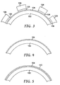
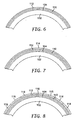
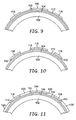
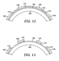
- tie layer 104 Once tie layer 104 has been formed, subsequent materials may be added to patterned roll. While particular processing steps are illustrated in FIGS. 4-13 , and will be discussed in detail with respect to the Example, a variety of opaque materials may be applied to tie layer 104. Suitable opaque materials include metals such as chrome, copper or aluminum, and curable polymers such as silicone and epoxy. Suitable materials may be applied and patterned using any suitable technique, such as sputtering, etching, and the like.
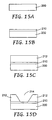
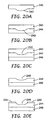
- FIGS. 15A-15D illustrate another potential method of forming opaque features on a non-machinable transparent substrate 200 that includes adding a machinable layer.
- a transparent epoxy layer 210 may be added to the transparent substrate 200 to help protect the transparent substrate during subsequent machining.
- an opaque epoxy layer 212 has been added on top of the transparent epoxy layer 210.
- opaque epoxy layer 212 has been machined using any suitable technique to form transparent feature 214.
- a web 122 is provided to the casting apparatus 120 from a main unwind spool (not shown).
- the exact nature of web 122 can vary widely, depending on the product being produced.
- the casting apparatus 120 is capable of handling a web 122 that is both flexible and transparent and/or opaque, as discussed previously.
- the web 122 is directed around various rollers 126 into the casting apparatus 120.
- the web 122 has had a pattern applied to both sides.
- a peel roll 182 may be present to assist in removal of the web 122 from second patterned roll 174.
- the web tension into and out of the casting apparatus is nearly constant.
- shaft resonance Reduction or elimination of shaft resonance is important as this is a source of registration error allowing pattern position control within the specified limits.
- Using a coupling 740 between the motor 733 and shaft 750 that is larger than general sizing schedules specify will also reduce shaft resonance caused by more flexible couplings.
- Bearing assemblies 760 are located in various locations to provide rotational support for the motor arrangement.
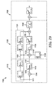
- motor arrangement 900 includes a motor 910 including a primary encoder 930 and a drive shaft 920.
- Drive shaft 920 is coupled to a driven shaft 940 of patterned roll 960 through a coupling 930.
- a secondary, or load, encoder 950 is coupled to the driven shaft 940.
- Motor arrangement 900 communicates with a control arrangement 965 to allow precision control of the patterned roll 960.
- Control arrangement 965 includes a drive module 966 and a program module 975.
- the program module 975 communicates with the drive module 966 via a line 977, for example, a SERCOS fiber network.
- the program module 975 is used to input parameters, such as set points, to the drive module 966.
- Drive module 966 receives input 480 volt, 3-phase power 915, rectifies it to DC, and distributes it via a power connection 973 to control the motor 910.
- Motor encoder 912 feeds a position signal to control module 966 via line 972.
- the secondary encoder 950 on the patterned roll 960 also feeds a position signal back to the drive module 966 via to line 971.
- the drive module 966 uses the encoder signals to precisely position the patterned roll 960.
- the control design to achieve the degree of registration is described in detail below.
- each patterned roll is controlled by a dedicated control arrangement.
- Dedicated control arrangements cooperate to control the registration between first and second patterned rolls.
- Each drive module communicates with and controls its respective motor assembly.
- the coated material is an electrically conductive material or an electroplate mask.
- an additional washing step can remove uncured material from the microreplicated pattern to produce a microreplicated features having no land areas and separated from one another.
- article 1202 may include lands, i.e. coated material-remaining on opaque web 1202 between adjacent elements.
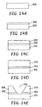
- a quartz cylinder 102 as seen in FIG. 4 was sputtered with a thin layer 104 of chrome, which acts as an adhesion layer between the quartz and the nickel layer to follow.
- a nickel metallization layer 110 was sputtered onto the chrome tie layer 104.
- a photoresist (SC Resists, Arch Semiconductor Photopolymers Company) layer 114 has been added on top of the copper layer 112.
- the height of the photoresist layer 114 ultimately sets the height of the features being formed on quartz cylinder 102.
- the photoresist layer 114 was formed to be 50 micrometers thick, and was softbaked at 115 degrees Celsius for 30 seconds prior to exposure.
- chrome sections 120 were plated onto the freshly exposed chrome layer 110, in between resist regions 116.
- Chrome sections 120 were plated using low current densities on the order of 1mA/17mm 2 . As the current density increases, even at levels as low as 20mA/17mm 2 , either internal stress was high, causing the chrome to peel off, or severe pitting occurred.
- the geometry of chrome sections 120 were determined by resist regions 116.
- the remaining cured photoresist, in resist regions 116 were removed using a basic solution.
- the remaining copper layer 112 was removed using a sodium persulfate bath as discussed above.
- the resulting patterned roll has opaque regions corresponding to nickel 110 and chrome sections 120, and transparent regions corresponding to where tie layer 104 is not covered by opaque material.
Claims (23)
- Article microrépliqué comprenant :un substrat opaque flexible ayant une première surface et une deuxième surface ;un premier motif microrépliqué déposé sur la première surface ; etun deuxième motif microrépliqué déposé sur la deuxième surface, le premier et le deuxième motif étant en concordance à moins de 100 micromètres ;dans lequel le substrat opaque flexible est opaque à l'énergie employée pour durcir le premier et le deuxième motif microrépliqué.
- Article selon la revendication 1, dans lequel le premier et le deuxième motif sont en concordance à moins de 10 micromètres.
- Article selon la revendication 1, dans lequel le premier et le deuxième motif sont en concordance à moins de 5 micromètres.
- Article selon les revendications 1 à 3, dans lequel le substrat opaque flexible est opaque au rayonnement ultraviolet.
- Article selon la revendication 4, dans lequel le substrat opaque flexible bloque au moins 98 pour cent du rayonnement ultraviolet qui est incident sur le substrat opaque flexible.
- Article selon les revendications 1 à 5, dans lequel le substrat opaque flexible comprend un polymère approprié pour former une carte de circuit imprimé flexible.
- Article selon la revendication 6, dans lequel le substrat opaque flexible comprend un polymère métallisé.
- Article selon les revendications 1 à 7, dans lequel le premier motif microrépliqué déposé comprend un polymère photodurcissable.
- Article selon les revendications 1 à 8, dans lequel le deuxième motif microrépliqué déposé comprend un polymère photodurcissable.
- Article selon les revendications 1 à 9, dans lequel le premier motif microrépliqué déposé comprend une pluralité d'éléments distincts, et au moins certains des éléments distincts sont discontinus des autres éléments distincts.
- Article selon les revendications 1 à 10, dans lequel le deuxième motif microrépliqué déposé comprend une pluralité d'éléments distincts, et au moins certains des éléments distincts sont discontinus des autres éléments distincts.
- Procédé de fabrication d'un article microrépliqué comportant une bande opaque ayant une première surface et une deuxième surface opposée, le procédé comprenant :le passage d'une bande opaque ayant une première surface et une deuxième surface opposée à travers un appareil de coulée comportant un premier rouleau à motif et un deuxième rouleau à motif ;la mise en contact d'un premier liquide avec le premier rouleau à motif et la première surface ;le durcissement du premier liquide pour créer un premier motif microrépliqué ;la mise en contact d'un deuxième liquide avec le deuxième rouleau à motif et la deuxième surface pendant que le premier motif microrépliqué est en contact avec le premier rouleau à motif ; etle durcissement du deuxième liquide pour créer un deuxième motif microrépliqué, le premier et le deuxième motif étant en concordance à moins de 100 micromètres ;dans lequel la bande opaque est opaque à l'énergie de durcissement utilisée pour durcir le premier et/ou le deuxième liquide.
- Procédé selon la revendication 12, dans lequel la mise en contact du premier liquide comprend la mise en contact d'une résine d'acrylate photodurcissable avec le premier rouleau à motif et la première surface.
- Procédé selon la revendication 12 ou 13, dans lequel la mise en contact du deuxième liquide comprend la mise en contact d'une résine d'acrylate photodurcissable avec le deuxième rouleau à motif et la deuxième surface.
- Procédé selon les revendications 12 à 14, dans lequel la mise en contact du premier liquide comprend la mise en contact d'un polymère isolant photodurcissable avec le premier rouleau à motif et la première surface.
- Procédé selon les revendications 12 à 15, dans lequel la mise en contact du deuxième liquide comprend la mise en contact d'un polymère isolant photodurcissable avec le deuxième rouleau à motif et la deuxième surface.
- Procédé de fabrication d'un article microrépliqué comprenant une bande opaque ayant un premier côté et un deuxième côté opposé, le procédé comprenant les étapes consistant à :déposer un matériau durcissable sur une bande ayant un premier côté et un deuxième côté opposé, ou sur un premier rouleau à motif et un deuxième rouleau à motif ;mettre la bande opaque en contact avec le premier rouleau à motif, le premier rouleau à motif comprenant une première pluralité de régions opaques disposées sur un substrat transparent ;durcir le matériau durcissable sur le premier côté de la bande pour former un premier motif microrépliqué ;mettre la bande opaque en contact avec le deuxième rouleau à motif, le deuxième rouleau à motif comprenant une deuxième pluralité de régions opaques disposées sur un substrat transparent ; etdurcir le matériau durcissable sur le deuxième côté de la bande pour former un deuxième motif microrépliqué ;dans lequel le premier et le deuxième côté de la bande sont modelés pendant que la bande est en mouvement continu de telle sorte que le premier et le deuxième motif sont maintenus en concordance continue à moins de 100 micromètres ; etdans lequel la bande opaque est opaque à l'énergie de durcissement utilisée pour durcir le matériau durcissable.
- Procédé selon la revendication 17, dans lequel le premier et le deuxième motif sont transférés au premier et au deuxième côté de la bande en concordance à moins de 5 micromètres.
- Procédé selon la revendication 18, dans lequel le dépôt du matériau durcissable sur la bande comprend :le dépôt du matériau durcissable sur le premier côté de la bande avant que le premier côté de la bande n'entre en contact avec le premier rouleau à motif ; etle dépôt du matériau durcissable sur le deuxième côté de la bande avant que le deuxième côté de la bande n'entre en contact avec le deuxième rouleau à motif.
- Procédé selon la revendication 18 ou 19, dans lequel le dépôt du matériau durcissable sur le premier rouleau à motif et le deuxième rouleau à motif comprend :le dépôt du matériau durcissable sur le premier rouleau à motif avant que le premier côté de la bande n'entre en contact avec le premier rouleau à motif ; etle dépôt du matériau durcissable sur le deuxième rouleau à motif avant que le deuxième côté de la bande n'entre en contact avec le deuxième rouleau à motif.
- Procédé selon les revendications 17 à 20, dans lequel au moins une partie du durcissement du matériau durcissable sur le premier côté de la bande se produit simultanément avec au moins une partie du durcissement du matériau durcissable sur le deuxième côté de la bande.
- Procédé selon les revendications 17 à 21, dans lequel le durcissement du matériau durcissable sur le premier côté de la bande comprend la soumission du matériau durcissable à un rayonnement ultraviolet qui traverse au moins partiellement le premier rouleau à motif.
- Procédé selon les revendications 17 à 22, dans lequel le durcissement du matériau durcissable sur le deuxième côté de la bande comprend la soumission du matériau durcissable à un rayonnement ultraviolet qui traverse au moins partiellement le deuxième rouleau à motif.
Applications Claiming Priority (2)
| Application Number | Priority Date | Filing Date | Title |
|---|---|---|---|
| US66143105P | 2005-03-09 | 2005-03-09 | |
| PCT/US2006/007975 WO2006098938A1 (fr) | 2005-03-09 | 2006-03-06 | Article microreplique et son procede de production |
Publications (2)
| Publication Number | Publication Date |
|---|---|
| EP1855815A1 EP1855815A1 (fr) | 2007-11-21 |
| EP1855815B1 true EP1855815B1 (fr) | 2011-03-02 |
Family
ID=36571982
Family Applications (1)
| Application Number | Title | Priority Date | Filing Date |
|---|---|---|---|
| EP06737183A Not-in-force EP1855815B1 (fr) | 2005-03-09 | 2006-03-06 | Article microreplique et son procede de production |
Country Status (10)
| Country | Link |
|---|---|
| US (1) | US7931841B2 (fr) |
| EP (1) | EP1855815B1 (fr) |
| JP (1) | JP4988698B2 (fr) |
| KR (1) | KR101312140B1 (fr) |
| CN (1) | CN101137449B (fr) |
| AT (1) | ATE500001T1 (fr) |
| BR (1) | BRPI0608701A2 (fr) |
| DE (1) | DE602006020416D1 (fr) |
| MX (1) | MX2007010907A (fr) |
| WO (1) | WO2006098938A1 (fr) |
Families Citing this family (20)
| Publication number | Priority date | Publication date | Assignee | Title |
|---|---|---|---|---|
| US7224529B2 (en) * | 2003-09-09 | 2007-05-29 | 3M Innovative Properties Company | Microreplicated article |
| US20050231809A1 (en) * | 2003-09-09 | 2005-10-20 | Carlson Daniel H | Microreplicated polarizing article |
| US7804649B2 (en) * | 2003-09-09 | 2010-09-28 | 3M Innovative Properties Company | Microreplicated achromatic lens |
| US7165959B2 (en) * | 2003-09-09 | 2007-01-23 | 3M Innovative Properties Company | Apparatus and method for producing two-sided patterned webs in registration |
| WO2006098940A1 (fr) * | 2005-03-09 | 2006-09-21 | 3M Innovative Properties Company | Article microreproduit dote d’une surface reduisant le moire |
| DE602006005638D1 (de) * | 2005-03-09 | 2009-04-23 | 3M Innovative Properties Co | Vorrichtung und verfahren zur herstellung eines mikroreplizierten artikels |
| US20060210770A1 (en) * | 2005-03-09 | 2006-09-21 | Nelson John C | Microreplicated article with defect-reducing surface |
| KR101300866B1 (ko) | 2005-03-09 | 2013-08-27 | 쓰리엠 이노베이티브 프로퍼티즈 컴파니 | 정합 상태로 된 양면형의 패터닝된 웨브를 제조하는 장치및 방법 |
| US7976741B2 (en) * | 2007-02-12 | 2011-07-12 | Ichia Technologies, Inc. | Method of manufacturing light guide plate of keypad |
| US20100252961A1 (en) * | 2009-04-06 | 2010-10-07 | 3M Innovative Properties Company | Optical film replication on low thermal diffusivity tooling with conformal coating |
| CN102959492B (zh) | 2010-06-25 | 2016-03-16 | 诺基亚技术有限公司 | 用户界面和相关设备及方法 |
| TW201202008A (en) * | 2010-07-12 | 2012-01-16 | Hon Hai Prec Ind Co Ltd | Device and method for making optical film |
| KR20120067163A (ko) * | 2010-12-15 | 2012-06-25 | 삼성모바일디스플레이주식회사 | 박막 증착 장치 및 이를 이용한 유기 발광 디스플레이 장치의 제조 방법 |
| TWI552861B (zh) * | 2012-02-08 | 2016-10-11 | 鴻海精密工業股份有限公司 | 導光膜製造裝置及製造方法 |
| CN103246006A (zh) * | 2012-02-10 | 2013-08-14 | 鸿富锦精密工业(深圳)有限公司 | 导光膜制造装置及制造方法 |
| US9868135B2 (en) | 2015-05-06 | 2018-01-16 | The Boeing Company | Aerodynamic microstructures having sub-microstructures |
| US9751618B2 (en) | 2015-05-06 | 2017-09-05 | The Boeing Company | Optical effects for aerodynamic microstructures |
| US9714083B2 (en) | 2015-05-06 | 2017-07-25 | The Boeing Company | Color applications for aerodynamic microstructures |
| US10105877B2 (en) | 2016-07-08 | 2018-10-23 | The Boeing Company | Multilayer riblet applique and methods of producing the same |
| CN113692135B (zh) * | 2021-10-26 | 2022-01-14 | 武汉大学 | 一种提高蚀刻过程中fpcb平整性的装置及方法 |
Family Cites Families (113)
| Publication number | Priority date | Publication date | Assignee | Title |
|---|---|---|---|---|
| US3241429A (en) * | 1962-05-14 | 1966-03-22 | Pid Corp | Pictorial parallax panoramagram units |
| US3374303A (en) * | 1964-02-14 | 1968-03-19 | Crown Zellerbach Corp | Method for manufacturing imprinted plastic film |
| US3551544A (en) * | 1965-12-06 | 1970-12-29 | Tenex Corp | Method of continuously forming an elongated cleated runner of plastic material |
| US3893795A (en) * | 1970-08-20 | 1975-07-08 | Rowland Dev Corp | Embossing rolls with areas of differential hardness |
| US3917772A (en) * | 1972-02-10 | 1975-11-04 | Grace W R & Co | Method for producing battery separator sheet |
| DE2632107C2 (de) * | 1975-07-16 | 1986-01-09 | Ludwig Dr. Vacallo Tessin Eigenmann | Rückstrahlaggregat für Markierungsmaterial zur horizontalen Straßenmarkierung |
| US4078416A (en) * | 1976-10-07 | 1978-03-14 | The Minster Machine Company | Method and apparatus for feeding strip stock into a machine |
| US4177304A (en) * | 1977-03-17 | 1979-12-04 | Beloit Corporation | Method of coating both sides of a travelling web |
| US6630970B2 (en) | 2001-07-02 | 2003-10-07 | 3M Innovative Properties Company | Polarizers for use with liquid crystal displays |
| US4249878A (en) * | 1979-05-10 | 1981-02-10 | K. R. Komarek, Inc. | Briquetting press |
| US4280978A (en) * | 1979-05-23 | 1981-07-28 | Monsanto Company | Process of embossing and perforating thermoplastic film |
| US4420502A (en) * | 1980-09-05 | 1983-12-13 | Conley Kenneth E | Apparatus and method for producing a flexible sheet material having a predetermined surface characteristic |
| US4414316A (en) * | 1980-09-05 | 1983-11-08 | Rexham Corporation | Composite lenticular screen sheet |
| DE3206164C2 (de) | 1981-03-16 | 1985-02-21 | Heinz Georg Hünibach Thun Baus | Vorrichtung zur Herstellung von Mehrschicht-Platten |
| ATE38485T1 (de) * | 1981-03-16 | 1988-11-15 | Heinz Georg Baus | Verfahren zur herstellung von mehrschichtplatten. |
| DE3567596D1 (en) * | 1984-03-08 | 1989-02-23 | Heinz Georg Baus | Apparatus for manufacturing sheets, and sheets manufactured by this apparatus |
| US4744936A (en) * | 1986-01-30 | 1988-05-17 | Plastic Film Corporation Of America | Process for embossing thermoplastic material |
| DE3609090A1 (de) * | 1986-03-18 | 1987-09-24 | Gao Ges Automation Org | Wertpapier mit darin eingelagertem sicherheitsfaden und verfahren zur herstellung derselben |
| US4836874A (en) * | 1987-01-30 | 1989-06-06 | Foster Michael S | Method of mass producing damage-resistant compact discs |
| US5164227A (en) * | 1987-06-19 | 1992-11-17 | Van Leer Metallized Products (Usa) Limited | Method for embossing a coated sheet with a diffraction or holographic pattern |
| US5028361A (en) * | 1987-11-09 | 1991-07-02 | Takeo Fujimoto | Method for molding a photosensitive composition |
| JP2692095B2 (ja) * | 1987-12-16 | 1997-12-17 | ソニー株式会社 | スクリーンの製造方法 |
| US5096401A (en) | 1989-06-26 | 1992-03-17 | Canon Kabushiki Kaisha | Apparatus for producing a substrate sheet for optical recording media |
| DE4001105C1 (fr) * | 1990-01-17 | 1991-08-08 | Hermann Berstorff Maschinenbau Gmbh, 3000 Hannover, De | |
| US6724536B2 (en) * | 1990-05-18 | 2004-04-20 | University Of Arkansas | Directional image lenticular window sheet |
| US5177637A (en) * | 1990-09-11 | 1993-01-05 | Nikon Corporation | Focusing screen including different height microlenses arranged in a cyclical pattern |
| JPH0580530A (ja) * | 1991-09-24 | 1993-04-02 | Hitachi Ltd | 薄膜パターン製造方法 |
| EP0534471A1 (fr) * | 1991-09-27 | 1993-03-31 | Toppan Printing Co., Ltd. | Stratifié composite et procédé de sa fabrication |
| JP3322351B2 (ja) * | 1992-04-22 | 2002-09-09 | 大日本印刷株式会社 | 両面レリーフパターン複製方法及び装置 |
| JP2756211B2 (ja) * | 1992-06-17 | 1998-05-25 | ワイケイケイ株式会社 | 両面に係合片を有する一体成形面ファスナーの製造方法及びその装置 |
| JP2833360B2 (ja) * | 1992-07-29 | 1998-12-09 | 凸版印刷株式会社 | 電離放射線照射によるエンボス成形方法 |
| DE4226906A1 (de) * | 1992-08-14 | 1994-02-17 | Basf Magnetics Gmbh | Anti-Kopier-Film oder -Schicht für Dokumente |
| US5330799A (en) * | 1992-09-15 | 1994-07-19 | The Phscologram Venture, Inc. | Press polymerization of lenticular images |
| KR0168879B1 (ko) * | 1992-12-25 | 1999-04-15 | 기따지마 요시또시 | 렌티큘러 렌즈, 면광원 및 액정 표시 장치 |
| US5448401A (en) * | 1992-12-25 | 1995-09-05 | Sony Corporation | Screen of projection display |
| US5333072A (en) * | 1992-12-31 | 1994-07-26 | Minnesota Mining And Manufacturing Company | Reflective liquid crystal display overhead projection system using a reflective linear polarizer and a fresnel lens |
| EP0623440B1 (fr) * | 1993-03-16 | 1997-09-10 | Koninklijke Philips Electronics N.V. | Procédé de et dispositif pour l'obtention d'un motif structuré avec une photoréserve réticulée sur la surface d'un substrat plat |
| DE69405451T2 (de) * | 1993-03-16 | 1998-03-12 | Koninkl Philips Electronics Nv | Verfahren und Vorrichtung zur Herstellung eines strukturierten Reliefbildes aus vernetztem Photoresist auf einer flachen Substratoberfläche |
| US5598280A (en) * | 1993-03-23 | 1997-01-28 | Dai Nippon Printing Co., Ltd. | Film lens and a surface light source using the same |
| US5691846A (en) * | 1993-10-20 | 1997-11-25 | Minnesota Mining And Manufacturing Company | Ultra-flexible retroreflective cube corner composite sheetings and methods of manufacture |
| US5579164A (en) | 1993-11-12 | 1996-11-26 | Pharos Technology Corporation | Spatially multiplexed image display system |
| US6025897A (en) | 1993-12-21 | 2000-02-15 | 3M Innovative Properties Co. | Display with reflective polarizer and randomizing cavity |
| US5759455A (en) * | 1994-07-08 | 1998-06-02 | Canon Kabushiki Kaisha | Roller-shaped stamper for fabricating optical scales |
| US5540147A (en) * | 1994-12-02 | 1996-07-30 | Corning Incorporated | Method for forming a contoured planarizing layer for a color filter |
| EP0871923A1 (fr) | 1995-06-26 | 1998-10-21 | Minnesota Mining And Manufacturing Company | Dispositifs transflectifs a transflecteur de polarisation reflechissant |
| US6130777A (en) * | 1996-05-16 | 2000-10-10 | Dai Nippon Printing Co., Ltd. | Lenticular lens sheet with both a base sheet having lenticular elements and a surface diffusing part having elements of elementary shape smaller than lenticular elements |
| US5914760A (en) | 1996-06-21 | 1999-06-22 | Casio Computer Co., Ltd. | Surface light source device and liquid crystal display device using the same |
| US5800723A (en) * | 1996-12-10 | 1998-09-01 | Motorola, Inc. | Process for fabricating flex circuits and product thereby |
| US6197397B1 (en) | 1996-12-31 | 2001-03-06 | 3M Innovative Properties Company | Adhesives having a microreplicated topography and methods of making and using same |
| JPH10211650A (ja) * | 1997-01-31 | 1998-08-11 | Asahi Chem Ind Co Ltd | 合成樹脂シート成形ロール設備 |
| US5922238A (en) * | 1997-02-14 | 1999-07-13 | Physical Optics Corporation | Method of making replicas and compositions for use therewith |
| US6280063B1 (en) * | 1997-05-09 | 2001-08-28 | 3M Innovative Properties Company | Brightness enhancement article |
| DE19721170A1 (de) * | 1997-05-21 | 1998-11-26 | Emtec Magnetics Gmbh | Verfahren und Vorrichtung zum Herstellen eines Films oder einer Schicht mit beidseitiger Oberflächenstruktur |
| US6577358B1 (en) * | 1997-06-25 | 2003-06-10 | Dai Nippon Printing Co., Ltd. | Lens film with conductive lens layer or conductive layer |
| CA2244324A1 (fr) | 1997-08-04 | 1999-02-04 | Hsm Holographic Systems Munchen Gmbh | Methode et appareil de fabrication d'une structure de surface sur un substrat, particulierement une surface holographique |
| US6074192A (en) * | 1997-09-11 | 2000-06-13 | Mikkelsen; Oeystein | Lenticular pattern forming roll and method for making the roll |
| CN1142451C (zh) | 1997-12-16 | 2004-03-17 | “尼奥匹克”俄罗斯联邦全国科技中心 | 偏振片和液晶显示元件 |
| US6024455A (en) | 1998-01-13 | 2000-02-15 | 3M Innovative Properties Company | Reflective article with concealed retroreflective pattern |
| CA2282853C (fr) * | 1998-01-30 | 2002-01-01 | James H. Stauffacher | Dispositif et procede d'impression et d'estampage de substrats allonges |
| EP1975649A1 (fr) * | 1998-02-18 | 2008-10-01 | Minnesota Mining And Manufacturing Company | Film optique |
| KR100604123B1 (ko) | 1998-08-05 | 2006-07-25 | 미쯔비시 레이온 가부시끼가이샤 | 렌즈 시트 및 그 제조방법 |
| US6149849A (en) * | 1998-08-14 | 2000-11-21 | The Procter & Gamble Copmany | Process and apparatus for making papermaking belt |
| US6187250B1 (en) | 1998-08-19 | 2001-02-13 | James Champagne | Continuous gel casting method and apparatus |
| US6266476B1 (en) | 1998-08-25 | 2001-07-24 | Physical Optics Corporation | Optical element having an integral surface diffuser |
| WO2000016157A1 (fr) * | 1998-09-16 | 2000-03-23 | Fujitsu Limited | Dispositif optique et dispositif d'affichage utilisant ce dispositif |
| JP2000183253A (ja) | 1998-12-14 | 2000-06-30 | Kyocera Corp | 半導体素子収納用パッケージ |
| JP2000275406A (ja) | 1999-03-29 | 2000-10-06 | Dainippon Printing Co Ltd | レンズシート及びその製造方法 |
| US6272275B1 (en) * | 1999-06-25 | 2001-08-07 | Corning Incorporated | Print-molding for process for planar waveguides |
| RU2261462C2 (ru) * | 1999-09-30 | 2005-09-27 | Конинклейке Филипс Электроникс Н.В. | Линзовое устройство (варианты) и множество линзовых устройств |
| US6845212B2 (en) | 1999-10-08 | 2005-01-18 | 3M Innovative Properties Company | Optical element having programmed optical structures |
| KR100647938B1 (ko) * | 1999-10-08 | 2006-11-17 | 스미토모 베이클리트 컴퍼니 리미티드 | 고분자 시트의 제조방법 및 광학 고분자 시트 |
| US6368682B1 (en) | 1999-10-22 | 2002-04-09 | 3M Innovative Properties Company | Composition and structures made therefrom |
| KR100343009B1 (ko) * | 2000-06-15 | 2002-07-02 | 권수식 | 고내식ㆍ고내흑변성 용융아연도금강판용 크로메이트 용액및 그 피막제조방법 |
| US6908295B2 (en) * | 2000-06-16 | 2005-06-21 | Avery Dennison Corporation | Process and apparatus for embossing precise microstructures and embossing tool for making same |
| AU7586801A (en) | 2000-07-11 | 2002-01-21 | 3M Innovative Properties Co | Backlight with structured sufaces |
| US6373636B1 (en) * | 2000-09-08 | 2002-04-16 | Kenneth E. Conley | Heat stabilized and dimensionally stable thin lenticular film |
| JP2002090889A (ja) * | 2000-09-14 | 2002-03-27 | Kuraray Co Ltd | 背面投射型スクリーン及びその製造方法 |
| JP2002113728A (ja) * | 2000-10-06 | 2002-04-16 | Mitsubishi Rayon Co Ltd | レンズシートの製造方法 |
| JP2002113738A (ja) | 2000-10-10 | 2002-04-16 | Nissha Printing Co Ltd | 成形同時加飾成形品の製造方法とこれに用いる成形同時加飾用シート |
| JP2002210915A (ja) * | 2001-01-22 | 2002-07-31 | Tokyo Kikai Seisakusho Ltd | 分割版胴を個別に駆動する多色刷平版印刷機 |
| KR100870800B1 (ko) * | 2001-02-07 | 2008-11-27 | 코닝 인코포레이티드 | 고정밀도 구경을 갖는 자기 정합 구경 마스크 |
| ITPS20010006A1 (it) * | 2001-02-23 | 2002-08-23 | Canti & Figli Srl | Procedimento e macchina atti ad ottenere goffrature su superfici verniciate di pannelli o di pellicole di rivestimento ed elementi ottenuti |
| EP1248160B8 (fr) | 2001-04-03 | 2009-11-04 | Sharp Kabushiki Kaisha | Dispositif de développement, procédé pour charger utilisé pour ceci, et appareil d'impression avec le dispositif de développement |
| DE60228943D1 (de) | 2001-04-10 | 2008-10-30 | Harvard College | Mikrolinse zur projektionslithographie und ihr herstellungsverfahren |
| EP1251365B1 (fr) | 2001-04-20 | 2004-02-25 | Matsushita Electric Industrial Co., Ltd. | Réseau de microlentilles et méthode de sa fabrication |
| US7420005B2 (en) | 2001-06-28 | 2008-09-02 | Dai Nippon Printing Co., Ltd. | Photocurable resin composition, finely embossed pattern-forming sheet, finely embossed transfer sheet, optical article, stamper and method of forming finely embossed pattern |
| US6863107B2 (en) * | 2001-10-02 | 2005-03-08 | Sca Hygiene Products Gmbh | Device for applying a spot embossing pattern to a web of multi-ply tissue paper |
| US6717749B2 (en) | 2001-11-01 | 2004-04-06 | Pentax Corporation | Cemented lens group |
| US20030108710A1 (en) * | 2001-12-07 | 2003-06-12 | General Electric Company | Articles bearing patterned microstructures and method of making |
| ATE465002T1 (de) | 2002-03-15 | 2010-05-15 | Procter & Gamble | Vorrichtung zum prägen und beschichten mit klebstoff |
| AT502319B1 (de) | 2002-04-11 | 2009-11-15 | Hueck Folien Gmbh | Substrate mit vorzugsweise transferierbaren schichten und/oder oberflächenstrukturen, verfahren zu deren herstellung und deren verwendung |
| US7140812B2 (en) * | 2002-05-29 | 2006-11-28 | 3M Innovative Properties Company | Diamond tool with a multi-tipped diamond |
| DE10242441A1 (de) * | 2002-09-11 | 2004-04-01 | Erco Leuchten Gmbh | Leuchte |
| US7210836B2 (en) * | 2002-09-19 | 2007-05-01 | Mitsubishi Denki Kabushiki Kaisha | Display unit and electronic apparatus with display unit |
| US6963184B2 (en) * | 2002-09-26 | 2005-11-08 | 3M Innovative Properties Company | Adaptable spatial notch filter |
| US7186004B2 (en) * | 2002-12-31 | 2007-03-06 | Karlton David Powell | Homogenizing optical sheet, method of manufacture, and illumination system |
| US7070406B2 (en) | 2003-04-29 | 2006-07-04 | Hewlett-Packard Development Company, L.P. | Apparatus for embossing a flexible substrate with a pattern carried by an optically transparent compliant media |
| US7330315B2 (en) | 2003-05-02 | 2008-02-12 | Reflexite Corporation | Light-redirecting optical structures |
| US7462305B2 (en) | 2003-05-23 | 2008-12-09 | Dai Nippon Printing Co., Ltd. | Optical sheet manufacturing method and optical sheet |
| JP4376128B2 (ja) | 2003-05-23 | 2009-12-02 | 大日本印刷株式会社 | 光学シート及びその製造方法 |
| US20050008821A1 (en) | 2003-07-07 | 2005-01-13 | Pricone Robert M. | Process and apparatus for fabricating precise microstructures and polymeric molds for making same |
| US7165959B2 (en) * | 2003-09-09 | 2007-01-23 | 3M Innovative Properties Company | Apparatus and method for producing two-sided patterned webs in registration |
| US20050231809A1 (en) * | 2003-09-09 | 2005-10-20 | Carlson Daniel H | Microreplicated polarizing article |
| US7224529B2 (en) * | 2003-09-09 | 2007-05-29 | 3M Innovative Properties Company | Microreplicated article |
| US7804649B2 (en) * | 2003-09-09 | 2010-09-28 | 3M Innovative Properties Company | Microreplicated achromatic lens |
| US7106517B2 (en) * | 2003-12-31 | 2006-09-12 | General Electric Company | Display optical films |
| US7808706B2 (en) | 2004-02-12 | 2010-10-05 | Tredegar Newco, Inc. | Light management films for displays |
| US20050224997A1 (en) | 2004-04-08 | 2005-10-13 | Tsung-Neng Liao | Method of fabricating optical substrate |
| KR101300866B1 (ko) | 2005-03-09 | 2013-08-27 | 쓰리엠 이노베이티브 프로퍼티즈 컴파니 | 정합 상태로 된 양면형의 패터닝된 웨브를 제조하는 장치및 방법 |
| DE602006005638D1 (de) | 2005-03-09 | 2009-04-23 | 3M Innovative Properties Co | Vorrichtung und verfahren zur herstellung eines mikroreplizierten artikels |
| US20060210770A1 (en) | 2005-03-09 | 2006-09-21 | Nelson John C | Microreplicated article with defect-reducing surface |
| WO2006098940A1 (fr) | 2005-03-09 | 2006-09-21 | 3M Innovative Properties Company | Article microreproduit dote d’une surface reduisant le moire |
| KR20070111544A (ko) | 2005-03-09 | 2007-11-21 | 쓰리엠 이노베이티브 프로퍼티즈 컴파니 | 미세 복제품 제조 장치 및 방법 |
-
2006
- 2006-03-06 US US11/369,372 patent/US7931841B2/en active Active
- 2006-03-06 JP JP2008500815A patent/JP4988698B2/ja not_active Expired - Fee Related
- 2006-03-06 MX MX2007010907A patent/MX2007010907A/es unknown
- 2006-03-06 WO PCT/US2006/007975 patent/WO2006098938A1/fr active Application Filing
- 2006-03-06 CN CN2006800077191A patent/CN101137449B/zh not_active Expired - Fee Related
- 2006-03-06 EP EP06737183A patent/EP1855815B1/fr not_active Not-in-force
- 2006-03-06 AT AT06737183T patent/ATE500001T1/de not_active IP Right Cessation
- 2006-03-06 BR BRPI0608701-9A patent/BRPI0608701A2/pt not_active Application Discontinuation
- 2006-03-06 DE DE602006020416T patent/DE602006020416D1/de active Active
- 2006-03-06 KR KR1020077020460A patent/KR101312140B1/ko active IP Right Grant
Also Published As
| Publication number | Publication date |
|---|---|
| KR101312140B1 (ko) | 2013-09-26 |
| CN101137449A (zh) | 2008-03-05 |
| EP1855815A1 (fr) | 2007-11-21 |
| US20060251803A1 (en) | 2006-11-09 |
| WO2006098938A1 (fr) | 2006-09-21 |
| KR20070108234A (ko) | 2007-11-08 |
| BRPI0608701A2 (pt) | 2010-01-19 |
| MX2007010907A (es) | 2007-12-05 |
| JP4988698B2 (ja) | 2012-08-01 |
| US7931841B2 (en) | 2011-04-26 |
| DE602006020416D1 (de) | 2011-04-14 |
| JP2008532806A (ja) | 2008-08-21 |
| CN101137449B (zh) | 2012-08-29 |
| ATE500001T1 (de) | 2011-03-15 |
Similar Documents
| Publication | Publication Date | Title |
|---|---|---|
| US8968629B2 (en) | Apparatus and method for producing two-sided patterned web in registration | |
| EP1855815B1 (fr) | Article microreplique et son procede de production | |
| EP1663618B1 (fr) | Appareil et procede de production de bandes a motifs double face alignees | |
| EP1874524B1 (fr) | Appareil et procede de fabrication d'un article microreproduit | |
| KR20060116803A (ko) | 미세복제된 물품 | |
| KR20070111544A (ko) | 미세 복제품 제조 장치 및 방법 |
Legal Events
| Date | Code | Title | Description |
|---|---|---|---|
| PUAI | Public reference made under article 153(3) epc to a published international application that has entered the european phase |
Free format text: ORIGINAL CODE: 0009012 |
|
| 17P | Request for examination filed |
Effective date: 20070919 |
|
| AK | Designated contracting states |
Kind code of ref document: A1 Designated state(s): AT BE BG CH CY CZ DE DK EE ES FI FR GB GR HU IE IS IT LI LT LU LV MC NL PL PT RO SE SI SK TR |
|
| 17Q | First examination report despatched |
Effective date: 20080111 |
|
| DAX | Request for extension of the european patent (deleted) | ||
| GRAP | Despatch of communication of intention to grant a patent |
Free format text: ORIGINAL CODE: EPIDOSNIGR1 |
|
| GRAS | Grant fee paid |
Free format text: ORIGINAL CODE: EPIDOSNIGR3 |
|
| GRAA | (expected) grant |
Free format text: ORIGINAL CODE: 0009210 |
|
| AK | Designated contracting states |
Kind code of ref document: B1 Designated state(s): AT BE BG CH CY CZ DE DK EE ES FI FR GB GR HU IE IS IT LI LT LU LV MC NL PL PT RO SE SI SK TR |
|
| REG | Reference to a national code |
Ref country code: GB Ref legal event code: FG4D |
|
| REG | Reference to a national code |
Ref country code: CH Ref legal event code: EP |
|
| REG | Reference to a national code |
Ref country code: IE Ref legal event code: FG4D |
|
| REF | Corresponds to: |
Ref document number: 602006020416 Country of ref document: DE Date of ref document: 20110414 Kind code of ref document: P |
|
| REG | Reference to a national code |
Ref country code: DE Ref legal event code: R096 Ref document number: 602006020416 Country of ref document: DE Effective date: 20110414 |
|
| REG | Reference to a national code |
Ref country code: NL Ref legal event code: VDEP Effective date: 20110302 |
|
| PG25 | Lapsed in a contracting state [announced via postgrant information from national office to epo] |
Ref country code: ES Free format text: LAPSE BECAUSE OF FAILURE TO SUBMIT A TRANSLATION OF THE DESCRIPTION OR TO PAY THE FEE WITHIN THE PRESCRIBED TIME-LIMIT Effective date: 20110613 Ref country code: LT Free format text: LAPSE BECAUSE OF FAILURE TO SUBMIT A TRANSLATION OF THE DESCRIPTION OR TO PAY THE FEE WITHIN THE PRESCRIBED TIME-LIMIT Effective date: 20110302 Ref country code: LV Free format text: LAPSE BECAUSE OF FAILURE TO SUBMIT A TRANSLATION OF THE DESCRIPTION OR TO PAY THE FEE WITHIN THE PRESCRIBED TIME-LIMIT Effective date: 20110302 Ref country code: GR Free format text: LAPSE BECAUSE OF FAILURE TO SUBMIT A TRANSLATION OF THE DESCRIPTION OR TO PAY THE FEE WITHIN THE PRESCRIBED TIME-LIMIT Effective date: 20110603 Ref country code: SE Free format text: LAPSE BECAUSE OF FAILURE TO SUBMIT A TRANSLATION OF THE DESCRIPTION OR TO PAY THE FEE WITHIN THE PRESCRIBED TIME-LIMIT Effective date: 20110302 |
|
| LTIE | Lt: invalidation of european patent or patent extension |
Effective date: 20110302 |
|
| PG25 | Lapsed in a contracting state [announced via postgrant information from national office to epo] |
Ref country code: NL Free format text: LAPSE BECAUSE OF FAILURE TO SUBMIT A TRANSLATION OF THE DESCRIPTION OR TO PAY THE FEE WITHIN THE PRESCRIBED TIME-LIMIT Effective date: 20110302 Ref country code: FI Free format text: LAPSE BECAUSE OF FAILURE TO SUBMIT A TRANSLATION OF THE DESCRIPTION OR TO PAY THE FEE WITHIN THE PRESCRIBED TIME-LIMIT Effective date: 20110302 Ref country code: SI Free format text: LAPSE BECAUSE OF FAILURE TO SUBMIT A TRANSLATION OF THE DESCRIPTION OR TO PAY THE FEE WITHIN THE PRESCRIBED TIME-LIMIT Effective date: 20110302 Ref country code: AT Free format text: LAPSE BECAUSE OF FAILURE TO SUBMIT A TRANSLATION OF THE DESCRIPTION OR TO PAY THE FEE WITHIN THE PRESCRIBED TIME-LIMIT Effective date: 20110302 Ref country code: CY Free format text: LAPSE BECAUSE OF FAILURE TO SUBMIT A TRANSLATION OF THE DESCRIPTION OR TO PAY THE FEE WITHIN THE PRESCRIBED TIME-LIMIT Effective date: 20110302 Ref country code: BG Free format text: LAPSE BECAUSE OF FAILURE TO SUBMIT A TRANSLATION OF THE DESCRIPTION OR TO PAY THE FEE WITHIN THE PRESCRIBED TIME-LIMIT Effective date: 20110602 |
|
| PG25 | Lapsed in a contracting state [announced via postgrant information from national office to epo] |
Ref country code: BE Free format text: LAPSE BECAUSE OF FAILURE TO SUBMIT A TRANSLATION OF THE DESCRIPTION OR TO PAY THE FEE WITHIN THE PRESCRIBED TIME-LIMIT Effective date: 20110302 |
|
| PG25 | Lapsed in a contracting state [announced via postgrant information from national office to epo] |
Ref country code: MC Free format text: LAPSE BECAUSE OF NON-PAYMENT OF DUE FEES Effective date: 20110331 Ref country code: EE Free format text: LAPSE BECAUSE OF FAILURE TO SUBMIT A TRANSLATION OF THE DESCRIPTION OR TO PAY THE FEE WITHIN THE PRESCRIBED TIME-LIMIT Effective date: 20110302 Ref country code: PT Free format text: LAPSE BECAUSE OF FAILURE TO SUBMIT A TRANSLATION OF THE DESCRIPTION OR TO PAY THE FEE WITHIN THE PRESCRIBED TIME-LIMIT Effective date: 20110704 |
|
| REG | Reference to a national code |
Ref country code: CH Ref legal event code: PL |
|
| PG25 | Lapsed in a contracting state [announced via postgrant information from national office to epo] |
Ref country code: CZ Free format text: LAPSE BECAUSE OF FAILURE TO SUBMIT A TRANSLATION OF THE DESCRIPTION OR TO PAY THE FEE WITHIN THE PRESCRIBED TIME-LIMIT Effective date: 20110302 Ref country code: SK Free format text: LAPSE BECAUSE OF FAILURE TO SUBMIT A TRANSLATION OF THE DESCRIPTION OR TO PAY THE FEE WITHIN THE PRESCRIBED TIME-LIMIT Effective date: 20110302 Ref country code: RO Free format text: LAPSE BECAUSE OF FAILURE TO SUBMIT A TRANSLATION OF THE DESCRIPTION OR TO PAY THE FEE WITHIN THE PRESCRIBED TIME-LIMIT Effective date: 20110302 Ref country code: IS Free format text: LAPSE BECAUSE OF FAILURE TO SUBMIT A TRANSLATION OF THE DESCRIPTION OR TO PAY THE FEE WITHIN THE PRESCRIBED TIME-LIMIT Effective date: 20110702 |
|
| REG | Reference to a national code |
Ref country code: IE Ref legal event code: MM4A |
|
| PLBE | No opposition filed within time limit |
Free format text: ORIGINAL CODE: 0009261 |
|
| STAA | Information on the status of an ep patent application or granted ep patent |
Free format text: STATUS: NO OPPOSITION FILED WITHIN TIME LIMIT |
|
| PG25 | Lapsed in a contracting state [announced via postgrant information from national office to epo] |
Ref country code: IE Free format text: LAPSE BECAUSE OF NON-PAYMENT OF DUE FEES Effective date: 20110306 Ref country code: LI Free format text: LAPSE BECAUSE OF NON-PAYMENT OF DUE FEES Effective date: 20110331 Ref country code: CH Free format text: LAPSE BECAUSE OF NON-PAYMENT OF DUE FEES Effective date: 20110331 |
|
| 26N | No opposition filed |
Effective date: 20111205 |
|
| GBPC | Gb: european patent ceased through non-payment of renewal fee |
Effective date: 20110602 |
|
| PG25 | Lapsed in a contracting state [announced via postgrant information from national office to epo] |
Ref country code: DK Free format text: LAPSE BECAUSE OF FAILURE TO SUBMIT A TRANSLATION OF THE DESCRIPTION OR TO PAY THE FEE WITHIN THE PRESCRIBED TIME-LIMIT Effective date: 20110302 Ref country code: PL Free format text: LAPSE BECAUSE OF FAILURE TO SUBMIT A TRANSLATION OF THE DESCRIPTION OR TO PAY THE FEE WITHIN THE PRESCRIBED TIME-LIMIT Effective date: 20110302 |
|
| REG | Reference to a national code |
Ref country code: FR Ref legal event code: ST Effective date: 20120210 |
|
| REG | Reference to a national code |
Ref country code: DE Ref legal event code: R097 Ref document number: 602006020416 Country of ref document: DE Effective date: 20111205 |
|
| PG25 | Lapsed in a contracting state [announced via postgrant information from national office to epo] |
Ref country code: FR Free format text: LAPSE BECAUSE OF NON-PAYMENT OF DUE FEES Effective date: 20110502 |
|
| PG25 | Lapsed in a contracting state [announced via postgrant information from national office to epo] |
Ref country code: IT Free format text: LAPSE BECAUSE OF FAILURE TO SUBMIT A TRANSLATION OF THE DESCRIPTION OR TO PAY THE FEE WITHIN THE PRESCRIBED TIME-LIMIT Effective date: 20110302 |
|
| PG25 | Lapsed in a contracting state [announced via postgrant information from national office to epo] |
Ref country code: GB Free format text: LAPSE BECAUSE OF NON-PAYMENT OF DUE FEES Effective date: 20110602 |
|
| PG25 | Lapsed in a contracting state [announced via postgrant information from national office to epo] |
Ref country code: LU Free format text: LAPSE BECAUSE OF NON-PAYMENT OF DUE FEES Effective date: 20110306 |
|
| PG25 | Lapsed in a contracting state [announced via postgrant information from national office to epo] |
Ref country code: TR Free format text: LAPSE BECAUSE OF FAILURE TO SUBMIT A TRANSLATION OF THE DESCRIPTION OR TO PAY THE FEE WITHIN THE PRESCRIBED TIME-LIMIT Effective date: 20110302 |
|
| PG25 | Lapsed in a contracting state [announced via postgrant information from national office to epo] |
Ref country code: HU Free format text: LAPSE BECAUSE OF FAILURE TO SUBMIT A TRANSLATION OF THE DESCRIPTION OR TO PAY THE FEE WITHIN THE PRESCRIBED TIME-LIMIT Effective date: 20110302 |
|
| PGFP | Annual fee paid to national office [announced via postgrant information from national office to epo] |
Ref country code: DE Payment date: 20210224 Year of fee payment: 16 |
|
| REG | Reference to a national code |
Ref country code: DE Ref legal event code: R119 Ref document number: 602006020416 Country of ref document: DE |
|
| PG25 | Lapsed in a contracting state [announced via postgrant information from national office to epo] |
Ref country code: DE Free format text: LAPSE BECAUSE OF NON-PAYMENT OF DUE FEES Effective date: 20221001 |