EP1852858A2 - Optisches Informationsaufzeichnungsmedium und zu dessen Herstellung verwendete Gussformvorrichtung - Google Patents
Optisches Informationsaufzeichnungsmedium und zu dessen Herstellung verwendete Gussformvorrichtung Download PDFInfo
- Publication number
- EP1852858A2 EP1852858A2 EP07251732A EP07251732A EP1852858A2 EP 1852858 A2 EP1852858 A2 EP 1852858A2 EP 07251732 A EP07251732 A EP 07251732A EP 07251732 A EP07251732 A EP 07251732A EP 1852858 A2 EP1852858 A2 EP 1852858A2
- Authority
- EP
- European Patent Office
- Prior art keywords
- area
- groove
- optical information
- recording medium
- information recording
- Prior art date
- Legal status (The legal status is an assumption and is not a legal conclusion. Google has not performed a legal analysis and makes no representation as to the accuracy of the status listed.)
- Ceased
Links
Images


Classifications
-
- G—PHYSICS
- G11—INFORMATION STORAGE
- G11B—INFORMATION STORAGE BASED ON RELATIVE MOVEMENT BETWEEN RECORD CARRIER AND TRANSDUCER
- G11B7/00—Recording or reproducing by optical means, e.g. recording using a thermal beam of optical radiation by modifying optical properties or the physical structure, reproducing using an optical beam at lower power by sensing optical properties; Record carriers therefor
- G11B7/24—Record carriers characterised by shape, structure or physical properties, or by the selection of the material
- G11B7/2407—Tracks or pits; Shape, structure or physical properties thereof
- G11B7/24073—Tracks
- G11B7/24076—Cross sectional shape in the radial direction of a disc, e.g. asymmetrical cross sectional shape
-
- G—PHYSICS
- G11—INFORMATION STORAGE
- G11B—INFORMATION STORAGE BASED ON RELATIVE MOVEMENT BETWEEN RECORD CARRIER AND TRANSDUCER
- G11B7/00—Recording or reproducing by optical means, e.g. recording using a thermal beam of optical radiation by modifying optical properties or the physical structure, reproducing using an optical beam at lower power by sensing optical properties; Record carriers therefor
- G11B7/24—Record carriers characterised by shape, structure or physical properties, or by the selection of the material
- G11B7/2407—Tracks or pits; Shape, structure or physical properties thereof
-
- G—PHYSICS
- G11—INFORMATION STORAGE
- G11B—INFORMATION STORAGE BASED ON RELATIVE MOVEMENT BETWEEN RECORD CARRIER AND TRANSDUCER
- G11B7/00—Recording or reproducing by optical means, e.g. recording using a thermal beam of optical radiation by modifying optical properties or the physical structure, reproducing using an optical beam at lower power by sensing optical properties; Record carriers therefor
- G11B7/24—Record carriers characterised by shape, structure or physical properties, or by the selection of the material
- G11B7/2407—Tracks or pits; Shape, structure or physical properties thereof
- G11B7/24073—Tracks
- G11B7/24079—Width or depth
-
- G—PHYSICS
- G11—INFORMATION STORAGE
- G11B—INFORMATION STORAGE BASED ON RELATIVE MOVEMENT BETWEEN RECORD CARRIER AND TRANSDUCER
- G11B7/00—Recording or reproducing by optical means, e.g. recording using a thermal beam of optical radiation by modifying optical properties or the physical structure, reproducing using an optical beam at lower power by sensing optical properties; Record carriers therefor
- G11B7/24—Record carriers characterised by shape, structure or physical properties, or by the selection of the material
- G11B7/26—Apparatus or processes specially adapted for the manufacture of record carriers
-
- G—PHYSICS
- G11—INFORMATION STORAGE
- G11B—INFORMATION STORAGE BASED ON RELATIVE MOVEMENT BETWEEN RECORD CARRIER AND TRANSDUCER
- G11B7/00—Recording or reproducing by optical means, e.g. recording using a thermal beam of optical radiation by modifying optical properties or the physical structure, reproducing using an optical beam at lower power by sensing optical properties; Record carriers therefor
- G11B7/24—Record carriers characterised by shape, structure or physical properties, or by the selection of the material
- G11B7/26—Apparatus or processes specially adapted for the manufacture of record carriers
- G11B7/263—Preparing and using a stamper, e.g. pressing or injection molding substrates
-
- G—PHYSICS
- G11—INFORMATION STORAGE
- G11B—INFORMATION STORAGE BASED ON RELATIVE MOVEMENT BETWEEN RECORD CARRIER AND TRANSDUCER
- G11B7/00—Recording or reproducing by optical means, e.g. recording using a thermal beam of optical radiation by modifying optical properties or the physical structure, reproducing using an optical beam at lower power by sensing optical properties; Record carriers therefor
- G11B7/007—Arrangement of the information on the record carrier, e.g. form of tracks, actual track shape, e.g. wobbled, or cross-section, e.g. v-shaped; Sequential information structures, e.g. sectoring or header formats within a track
- G11B7/00736—Auxiliary data, e.g. lead-in, lead-out, Power Calibration Area [PCA], Burst Cutting Area [BCA], control information
Definitions
- the present invention relates to a write-once optical information recording medium and an apparatus used for manufacturing the same. Specifically, the present invention relates to an optical information recording medium for recording with laser light at a wavelength of 360 to 450 nm (so-called blue laser light) using a semiconductor laser and to a mold apparatus used for manufacturing the same.
- the optical information recording media each include a recording layer using an organic dye compound so that the organic dye compound is decomposed or deteriorated by absorption of laser light to obtain, as a degree of modulation, a change in optical properties of the laser light at a recording/reproduction wavelength, for performing recording and reproduction.
- the optical information recording media each include a reflective layer, a recording layer, and a protective layer which are formed on a substrate, a spiral groove referred to as a "groove" being formed in a portion (recording area) of the substrate in which the recording layer is to be formed.
- a spiral groove referred to as a "groove" being formed in a portion (recording area) of the substrate in which the recording layer is to be formed.
- pits are formed in the grooves.
- the recording area is divided into a preformat area in which recording condition data such as media ID and laser power is previously stored, and a data area in which information is recorded by a user.
- the two areas have different groove spacings (track pitch), and the track pitch in the preformat area is wider than that in the data area.
- a Low-to-High system optical information recording medium has the tendency that a push-pull (NPPb) signal is increased.
- NPPb push-pull
- the NPPb signal is further increased, thereby causing the problem of failing to effect tracking.
- an object of the present invention to provide an optical information recording medium capable of suppressing an increase in NPPb signal in a preformat area to obtain a satisfactory push-pull signal in recording.
- an optical information recording medium includes at least a substrate on which a groove is formed in a recording area, a recording layer containing an organic dye, and a reflective layer.
- the recording area has a preformat area and a data area, the groove in the preformat area being narrower or shallower than that in the data area.
- the groove in the preformat area preferably has a V-shaped cross-section taken along the diameter direction of the recording medium.
- the groove in the preformat area is narrowed to decrease a signal difference detected by a photodetector, thereby suppressing an increase in NPPb signal.
- the present invention also provides a mold apparatus used for molding a substrate on which a groove is formed in a recording area in manufacturing an optical information recording medium, the mold apparatus including an upper mold, a lower mold, and a stamper.
- the stamper has a projection for forming the groove at a position corresponding to the recording area, the projection at a position corresponding to the preformat area being narrower or lower than that at a position corresponding to the data area.
- the present invention it is possible to easily form the substrate in which the groove in the preformat area is narrower or shallower than that in the data area, thereby permitting the manufacture of an optical information recording medium in which a NPPb signal in the preformat area is small.
- Fig. 1 is a schematic plan view showing a recording area, a preformat area, and a data area of an optical information recording medium
- Fig. 2 is a schematic view showing a portion of a section of an optical formation recording medium taken along the diameter direction according to an embodiment of the present invention
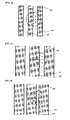
- Fig. 3 is a schematic view showing a state in which a groove in a data area is scanned with laser light.
- Fig. 4 is a schematic view showing a scanning state in a preformat area of a conventional optical information recording medium
- Fig. 5 is a schematic view showing a scanning state in a preformat area of an optical information recording medium according to an embodiment of the present invention
- Fig. 6 is a schematic view showing a mold apparatus used for manufacturing an optical information recording medium according to an embodiment of the present invention.
- Fig. 7 is a schematic view showing a portion of a section of a stamper used for manufacturing an optical information recording medium according to an embodiment of the present invention.
- Fig. 1 is a schematic plan view showing a recording area, a preformat area, and a data area of an optical information recording medium.
- Fig. 2 is a schematic view showing a portion of a section of an optical information recording medium taken along the diameter direction according to an embodiment of the present invention. As shown in Fig.
- an optical information recording medium 1 includes a reflective layer 3 composed of a metal layer with high reflectance, such as aluminum; a recording layer 4 containing an azo or cyanine dye; a transparent intermediate layer 5 composed of aluminum nitride; and a light transmitting layer 6 composed of a polycarbonate sheet, which are formed on a substrate of polycarbonate in that order with an adhesive provided between the intermediate layer 5 and the light transmitting layer 6.
- the recording area is divided into the data area and the preformat area.
- the width W2 of groove GV2 in the preformat area is smaller than the width W1 of groove GV1 in the data area.
- the track pitch TP2 in the preformat area is wider than the track pick TP1 in the data area.
- the depth D2 of the groove GV2 is smaller than the depth D1 of the groove GV1.
- Fig. 3 is a schematic view showing a state in which the groove in the data area is scanned with laser light.
- Fig. 4 is a schematic view showing a scanning state in a preformat area of a conventional optical information recording medium.
- Fig. 5 is a schematic view showing a scanning state in the preformat area of the optical information recording medium according to the present invention.
- Fig. 3 shows a state in which the groove GV is scanned with a beam spot applied from a pick-up and return light is received by the photodetector PD.
- the ratio of a portion overlapping the groove GV in the areas C and D is higher than that in the areas A and B. Since the land LD and the groove GV have a difference in brightness, a signal difference occurs according to the ratio of a portion overlapping the groove GV, thereby producing a NPPb signal.
- the width of the groove GV is the same as that in the data area, but the width of the land LD is larger than that in the data area, i.e., the track pitch is increased.
- a portion overlapping the groove GV in the areas A and B of the photodetector PD is decreased to increase a signal difference between the areas A and B and the areas C and D. Consequently, the NPPb signal is increased.
- the width of the groove GV in the preformat area is decreased so that a portion of the groove GV overlapping the photodetector PD is decreased. Accordingly, a signal difference between the areas A and B and the areas C and D is decreased to decrease the NPPb signal.
- both the width and the depth of the groove in the preformat area are smaller than those in the data area. However, even when at least one of the width and the depth of the groove in the preformat area is smaller than that in the data area, the effect of the present invention can be exhibited.
- the optical information recording medium 1 of the present invention is manufactured as follows: First, a polycarbonate resin is molded into a disk shape by injection molding using a mold apparatus 14 as shown in Fig. 6.
- the mold apparatus 14 is provided with an upper mold 11, a lower mold 12, and a stamper 10 formed in the space formed between the upper and lower molds 11 and 12, a groove pattern being formed on the stamper 10.
- the mold apparatus 14 is further provided with a stamper presser 13 for fixing the stamper 10.
- Fig. 7 shows a portion of a section of the stamper 10.
- a projection TK2 for forming the groove which has an inverted V-shaped cross-section, is formed in a portion corresponding to the preformat area.
- a projection TK1 which has a trapezoidal cross-section, is formed in a portion corresponding to the date area.
- the width L2 of the projection TK2 is smaller than the width L1 of the projection TK1.
- the height T2 of the projection TK2 is smaller than the height T1 of the projection TK1.
- the substrate 2 used for the optical information recording medium of the present invention can be formed.
- a metal layer is formed on the substrate 2 by sputtering to form the reflective layer 3.
- a dye solution is applied on the reflective layer 3 by spin coating and then dried to form the recording layer 4.
- the intermediate layer 5 is formed on the recording layer 4 by sputtering according to demand, and the light transmitting layer 6 composed of polycarbonate is bonded to the intermediate layer 5 through an adhesive. As a result, the optical information recording medium 1 is formed.
- a polycarbonate substrate having a portion corresponding to a preformat area with a track pitch of 0.35 ⁇ m and a groove width of 0.12 ⁇ m and a portion corresponding to a data area with a track pitch of 0.32 ⁇ m and a groove width of 0.18 ⁇ m was formed by injection molding to prepare a disk-shaped substrate having an outer diameter of 120 mm and a thickness of 1.1 mm.
- a substrate having a portion corresponding to a preformat area with a track pitch of 0.35 ⁇ m and a groove width of 0.18 ⁇ m and a portion corresponding to a data area with a track pitch of 0.32 ⁇ m and a groove width of 0.18 ⁇ m was formed by the same method as the above.
- a reflective layer composed of silver was formed to a thickness of 60 nm on each of the substrates by sputtering.
- a dye solution prepared by dissolving an azo dye represented by formula 1 below in a TFP (tetrafluoropropanol) solvent was applied by spin coating and then dried at a temperature of 80°C for 30 minutes to form a recording layer.
- a and A' represent the same or different heterocyclic rings each containing at least one heteroatom selected from a nitrogen atom, an oxygen atom, a sulfur atom, a selenium atom, and a tellurium atom
- R21 and R24 each independently represent a hydrogen atom or a substituent
- Y21 and Y22 represent the same or different heteroatoms selected from the Group XVI elements in the periodic table.
- a transparent material composed of aluminum nitride was formed to a thickness of 20 nm on the recording layer by sputtering to form an intermediate layer.
- a polycarbonate sheet of 0.1 mm in thickness was bonded to the intermediate layer using an acrylic transparent adhesive to prepare an optical information recording medium.
- the resultant optical information recording media were evaluated with respect to recording/reproduction characteristics (NPPb, Jitter) at a wavelength of 405 nm, a numerical aperture NA of 0.85, and a linear speed of 4.92 m/s using a commercial recording/reproduction apparatus (DDU-1000 manufactured by Pulstec Industrial Co., Ltd.). The results are shown in Table 1.
- the example of the present invention has the effect of decreasing NPPb in the preformat area. Therefore, an optical information recording medium capable of higher-density and higher-speed recording can be realized.
Landscapes
- Engineering & Computer Science (AREA)
- Manufacturing & Machinery (AREA)
- Optical Record Carriers And Manufacture Thereof (AREA)
- Manufacturing Optical Record Carriers (AREA)
Applications Claiming Priority (1)
| Application Number | Priority Date | Filing Date | Title |
|---|---|---|---|
| JP2006150626A JP2007299503A (ja) | 2006-04-28 | 2006-04-28 | 光情報記録媒体及びその製造に用いる金型装置 |
Publications (2)
| Publication Number | Publication Date |
|---|---|
| EP1852858A2 true EP1852858A2 (de) | 2007-11-07 |
| EP1852858A3 EP1852858A3 (de) | 2008-01-23 |
Family
ID=38294095
Family Applications (1)
| Application Number | Title | Priority Date | Filing Date |
|---|---|---|---|
| EP07251732A Ceased EP1852858A3 (de) | 2006-04-28 | 2007-04-24 | Optisches Informationsaufzeichnungsmedium und zu dessen Herstellung verwendete Gussformvorrichtung |
Country Status (6)
| Country | Link |
|---|---|
| US (1) | US7859982B2 (de) |
| EP (1) | EP1852858A3 (de) |
| JP (1) | JP2007299503A (de) |
| KR (1) | KR100904686B1 (de) |
| CN (1) | CN101064140B (de) |
| TW (1) | TW200809853A (de) |
Families Citing this family (2)
| Publication number | Priority date | Publication date | Assignee | Title |
|---|---|---|---|---|
| US7987046B1 (en) | 2007-04-04 | 2011-07-26 | Garmin Switzerland Gmbh | Navigation device with improved user interface and mounting features |
| US8873531B2 (en) * | 2010-05-03 | 2014-10-28 | Intel Corporation | Device, system and method of indicating station-specific information within a wireless communication |
Citations (3)
| Publication number | Priority date | Publication date | Assignee | Title |
|---|---|---|---|---|
| EP0762392B1 (de) | 1995-08-23 | 2001-11-14 | Mitsui Chemicals, Inc. | Optische Aufzeichnungsmedien |
| EP1296318A1 (de) | 2001-09-10 | 2003-03-26 | Ricoh Company, Ltd. | Optisches Informationsspeichermedium und Verfahren zum Speichern von Informationen auf diesem Medium |
| US6906993B2 (en) | 2001-06-15 | 2005-06-14 | Ritek Corporation | Hybrid optical disc having depths of pits as function of wavelength & pre-pits width which are function of track pitch within certain range |
Family Cites Families (12)
| Publication number | Priority date | Publication date | Assignee | Title |
|---|---|---|---|---|
| US5144552A (en) * | 1986-07-25 | 1992-09-01 | Ricoh Company, Ltd. | Optical information storage medium having grooves and pits with specific depths, respectively |
| JP2548186B2 (ja) * | 1987-04-13 | 1996-10-30 | パイオニア株式会社 | 案内溝付光デイスク |
| US5553051A (en) * | 1987-09-04 | 1996-09-03 | Hitachi, Ltd. | Increased intensity optical recording medium with adjacent grooves of different optical depth and a method and apparatus for reproducing the same |
| JPH09180262A (ja) * | 1995-12-27 | 1997-07-11 | Hitachi Maxell Ltd | 光記録媒体 |
| JP3065529B2 (ja) * | 1996-03-12 | 2000-07-17 | 株式会社リコー | 光情報記録媒体および光情報記録媒体のトラッキングサーボ方法 |
| DE69731411T2 (de) * | 1996-06-14 | 2006-03-02 | Mitsubishi Chemical Corp. | Optische Phasenänderungsscheibe |
| WO2001065552A1 (en) | 2000-02-28 | 2001-09-07 | Fujitsu Limited | Optical disk |
| JP2001273682A (ja) * | 2000-03-29 | 2001-10-05 | Victor Co Of Japan Ltd | 記録型ディスク及びその製造方法 |
| AU2001246913A1 (en) * | 2000-08-28 | 2002-03-13 | Nikon Corporation | Optical information recording medium, stamper, and method of manufacturing stamper |
| CN1220981C (zh) * | 2001-10-15 | 2005-09-28 | 日本胜利株式会社 | 信息记录载体 |
| JP3714331B2 (ja) * | 2003-02-14 | 2005-11-09 | ソニー株式会社 | 光記録媒体、光記録媒体製造用原盤、記録再生装置および記録再生方法 |
| JP2005302272A (ja) | 2004-03-18 | 2005-10-27 | Ricoh Co Ltd | 光情報記録媒体及びその記録再生方法 |
-
2006
- 2006-04-28 JP JP2006150626A patent/JP2007299503A/ja not_active Withdrawn
-
2007
- 2007-03-13 TW TW096108562A patent/TW200809853A/zh not_active IP Right Cessation
- 2007-04-16 CN CN2007100969231A patent/CN101064140B/zh not_active Expired - Fee Related
- 2007-04-18 KR KR1020070038051A patent/KR100904686B1/ko not_active Expired - Fee Related
- 2007-04-24 EP EP07251732A patent/EP1852858A3/de not_active Ceased
- 2007-04-25 US US11/740,179 patent/US7859982B2/en not_active Expired - Fee Related
Patent Citations (3)
| Publication number | Priority date | Publication date | Assignee | Title |
|---|---|---|---|---|
| EP0762392B1 (de) | 1995-08-23 | 2001-11-14 | Mitsui Chemicals, Inc. | Optische Aufzeichnungsmedien |
| US6906993B2 (en) | 2001-06-15 | 2005-06-14 | Ritek Corporation | Hybrid optical disc having depths of pits as function of wavelength & pre-pits width which are function of track pitch within certain range |
| EP1296318A1 (de) | 2001-09-10 | 2003-03-26 | Ricoh Company, Ltd. | Optisches Informationsspeichermedium und Verfahren zum Speichern von Informationen auf diesem Medium |
Also Published As
| Publication number | Publication date |
|---|---|
| US20070258348A1 (en) | 2007-11-08 |
| HK1106058A1 (zh) | 2008-02-29 |
| TW200809853A (en) | 2008-02-16 |
| TWI367483B (de) | 2012-07-01 |
| KR20070106405A (ko) | 2007-11-01 |
| CN101064140B (zh) | 2010-05-26 |
| US7859982B2 (en) | 2010-12-28 |
| CN101064140A (zh) | 2007-10-31 |
| JP2007299503A (ja) | 2007-11-15 |
| EP1852858A3 (de) | 2008-01-23 |
| KR100904686B1 (ko) | 2009-06-25 |
Similar Documents
| Publication | Publication Date | Title |
|---|---|---|
| US6287660B1 (en) | Optical recording medium and its substrate | |
| EP1758109B1 (de) | Optisches Informationsaufzeichnungsmedium | |
| EP1414029A2 (de) | Optisches Aufzeichnungsmedium und Verfahren zu dessen Herstellung | |
| CA2396246C (en) | Optical recording medium with high density track pitch and optical disk device for recording and playback of the same | |
| US6203877B1 (en) | Optical information recording medium | |
| EP1852858A2 (de) | Optisches Informationsaufzeichnungsmedium und zu dessen Herstellung verwendete Gussformvorrichtung | |
| JP2004082406A (ja) | 光記録媒体 | |
| US6721265B1 (en) | High-density optical information recording medium and a substrate and a stamper for the manufacture thereof | |
| US6521317B2 (en) | Optical recording medium | |
| JPWO2003003361A1 (ja) | 光記録媒体 | |
| KR100309115B1 (ko) | 광학 정보 기록 매체 및 그 제조방법 | |
| US6839318B2 (en) | Optical information recording medium having ultraviolet-curing resin and adhesive layers and method of manufacturing same | |
| US20040241575A1 (en) | Optical disk and method and apparatus for manufacturing the same | |
| JP4345246B2 (ja) | 光学記録媒体 | |
| HK1106058B (en) | Opitical information recording medium and mold apparatus for manufacturing the same | |
| KR20010090164A (ko) | 고밀도 광기록매체 | |
| JP4224071B2 (ja) | 光記録媒体 | |
| JPH10334507A (ja) | 光情報記録媒体 | |
| US6961302B2 (en) | Method and structure for intensifying track seeking signals from an optical disk | |
| EP1760700A1 (de) | Optisches informationsaufzeichnungsmedium und optisches informationsaufzeichnungs-/-wiedergabesystem | |
| JP2004327016A (ja) | 光記録ディスク | |
| JP2003109225A (ja) | 光記録媒体及びその製造方法 | |
| JP2003338078A (ja) | 光記録媒体及び記録方法 | |
| JP2005129199A (ja) | 光記録媒体 | |
| JP2007062206A (ja) | 色素、光記録材料、及び光記録媒体。 |
Legal Events
| Date | Code | Title | Description |
|---|---|---|---|
| PUAI | Public reference made under article 153(3) epc to a published international application that has entered the european phase |
Free format text: ORIGINAL CODE: 0009012 |
|
| AK | Designated contracting states |
Kind code of ref document: A2 Designated state(s): AT BE BG CH CY CZ DE DK EE ES FI FR GB GR HU IE IS IT LI LT LU LV MC MT NL PL PT RO SE SI SK TR |
|
| AX | Request for extension of the european patent |
Extension state: AL BA HR MK YU |
|
| PUAL | Search report despatched |
Free format text: ORIGINAL CODE: 0009013 |
|
| AK | Designated contracting states |
Kind code of ref document: A3 Designated state(s): AT BE BG CH CY CZ DE DK EE ES FI FR GB GR HU IE IS IT LI LT LU LV MC MT NL PL PT RO SE SI SK TR |
|
| AX | Request for extension of the european patent |
Extension state: AL BA HR MK YU |
|
| 17P | Request for examination filed |
Effective date: 20080627 |
|
| AKX | Designation fees paid |
Designated state(s): AT BE BG CH CY CZ DE DK EE ES FI FR GB GR HU IE IS IT LI LT LU LV MC MT NL PL PT RO SE SI SK TR |
|
| 17Q | First examination report despatched |
Effective date: 20081106 |
|
| STAA | Information on the status of an ep patent application or granted ep patent |
Free format text: STATUS: THE APPLICATION HAS BEEN REFUSED |
|
| 18R | Application refused |
Effective date: 20101022 |