EP1850353A1 - Conductive film - Google Patents
Conductive film Download PDFInfo
- Publication number
- EP1850353A1 EP1850353A1 EP05790574A EP05790574A EP1850353A1 EP 1850353 A1 EP1850353 A1 EP 1850353A1 EP 05790574 A EP05790574 A EP 05790574A EP 05790574 A EP05790574 A EP 05790574A EP 1850353 A1 EP1850353 A1 EP 1850353A1
- Authority
- EP
- European Patent Office
- Prior art keywords
- film
- conductive
- coating solution
- conductive portion
- network structure
- Prior art date
- Legal status (The legal status is an assumption and is not a legal conclusion. Google has not performed a legal analysis and makes no representation as to the accuracy of the status listed.)
- Withdrawn
Links
- 229910052751 metal Inorganic materials 0.000 claims description 40
- 239000002184 metal Substances 0.000 claims description 40
- RYGMFSIKBFXOCR-UHFFFAOYSA-N Copper Chemical group [Cu] RYGMFSIKBFXOCR-UHFFFAOYSA-N 0.000 claims description 24
- 229910052802 copper Inorganic materials 0.000 claims description 18
- 239000010949 copper Substances 0.000 claims description 18
- 239000002245 particle Substances 0.000 claims description 17
- 238000001035 drying Methods 0.000 claims description 8
- 229920001940 conductive polymer Polymers 0.000 claims description 7
- 239000000470 constituent Substances 0.000 claims description 5
- 239000010408 film Substances 0.000 description 158
- 239000000243 solution Substances 0.000 description 155
- 238000000576 coating method Methods 0.000 description 145
- 239000011248 coating agent Substances 0.000 description 141
- 238000000034 method Methods 0.000 description 46
- 239000010419 fine particle Substances 0.000 description 30
- 239000002585 base Substances 0.000 description 27
- 239000000203 mixture Substances 0.000 description 27
- 238000007747 plating Methods 0.000 description 22
- BQCADISMDOOEFD-UHFFFAOYSA-N Silver Chemical compound [Ag] BQCADISMDOOEFD-UHFFFAOYSA-N 0.000 description 21
- 229920000447 polyanionic polymer Polymers 0.000 description 21
- 229920000123 polythiophene Polymers 0.000 description 20
- 229910052709 silver Inorganic materials 0.000 description 20
- 239000004332 silver Substances 0.000 description 20
- XLYOFNOQVPJJNP-UHFFFAOYSA-N water Substances O XLYOFNOQVPJJNP-UHFFFAOYSA-N 0.000 description 20
- 239000007787 solid Substances 0.000 description 17
- 229920006267 polyester film Polymers 0.000 description 15
- -1 polypropylene Polymers 0.000 description 15
- 150000001875 compounds Chemical class 0.000 description 14
- 229920000642 polymer Polymers 0.000 description 13
- 229920002799 BoPET Polymers 0.000 description 12
- 239000004593 Epoxy Substances 0.000 description 10
- KDLHZDBZIXYQEI-UHFFFAOYSA-N Palladium Chemical compound [Pd] KDLHZDBZIXYQEI-UHFFFAOYSA-N 0.000 description 10
- 239000002253 acid Substances 0.000 description 10
- 239000007864 aqueous solution Substances 0.000 description 10
- 239000003431 cross linking reagent Substances 0.000 description 10
- 238000010438 heat treatment Methods 0.000 description 10
- 230000000052 comparative effect Effects 0.000 description 9
- MTHSVFCYNBDYFN-UHFFFAOYSA-N diethylene glycol Chemical compound OCCOCCO MTHSVFCYNBDYFN-UHFFFAOYSA-N 0.000 description 9
- 238000002156 mixing Methods 0.000 description 9
- RTZKZFJDLAIYFH-UHFFFAOYSA-N Diethyl ether Chemical compound CCOCC RTZKZFJDLAIYFH-UHFFFAOYSA-N 0.000 description 8
- 229920001577 copolymer Polymers 0.000 description 8
- 229920005989 resin Polymers 0.000 description 8
- 239000011347 resin Substances 0.000 description 8
- 238000007650 screen-printing Methods 0.000 description 8
- 238000002834 transmittance Methods 0.000 description 8
- LYCAIKOWRPUZTN-UHFFFAOYSA-N Ethylene glycol Chemical compound OCCO LYCAIKOWRPUZTN-UHFFFAOYSA-N 0.000 description 7
- 238000004519 manufacturing process Methods 0.000 description 7
- 239000000463 material Substances 0.000 description 7
- 229920000728 polyester Polymers 0.000 description 7
- VEXZGXHMUGYJMC-UHFFFAOYSA-N Hydrochloric acid Chemical compound Cl VEXZGXHMUGYJMC-UHFFFAOYSA-N 0.000 description 6
- KFZMGEQAYNKOFK-UHFFFAOYSA-N Isopropanol Chemical compound CC(C)O KFZMGEQAYNKOFK-UHFFFAOYSA-N 0.000 description 6
- PXHVJJICTQNCMI-UHFFFAOYSA-N Nickel Chemical compound [Ni] PXHVJJICTQNCMI-UHFFFAOYSA-N 0.000 description 6
- 239000011889 copper foil Substances 0.000 description 6
- 230000000694 effects Effects 0.000 description 6
- QQVIHTHCMHWDBS-UHFFFAOYSA-N isophthalic acid Chemical compound OC(=O)C1=CC=CC(C(O)=O)=C1 QQVIHTHCMHWDBS-UHFFFAOYSA-N 0.000 description 6
- 239000004973 liquid crystal related substance Substances 0.000 description 6
- 229920000172 poly(styrenesulfonic acid) Polymers 0.000 description 6
- 229920001225 polyester resin Polymers 0.000 description 6
- 239000004645 polyester resin Substances 0.000 description 6
- 229920000139 polyethylene terephthalate Polymers 0.000 description 6
- 239000005020 polyethylene terephthalate Substances 0.000 description 6
- 229940005642 polystyrene sulfonic acid Drugs 0.000 description 6
- 238000007639 printing Methods 0.000 description 6
- 239000000126 substance Substances 0.000 description 6
- 238000005530 etching Methods 0.000 description 5
- 229910052763 palladium Inorganic materials 0.000 description 5
- GKWLILHTTGWKLQ-UHFFFAOYSA-N 2,3-dihydrothieno[3,4-b][1,4]dioxine Chemical compound O1CCOC2=CSC=C21 GKWLILHTTGWKLQ-UHFFFAOYSA-N 0.000 description 4
- KKEYFWRCBNTPAC-UHFFFAOYSA-N Terephthalic acid Chemical compound OC(=O)C1=CC=C(C(O)=O)C=C1 KKEYFWRCBNTPAC-UHFFFAOYSA-N 0.000 description 4
- 125000004432 carbon atom Chemical group C* 0.000 description 4
- 238000005266 casting Methods 0.000 description 4
- 230000001788 irregular Effects 0.000 description 4
- 239000008188 pellet Substances 0.000 description 4
- BASFCYQUMIYNBI-UHFFFAOYSA-N platinum Chemical compound [Pt] BASFCYQUMIYNBI-UHFFFAOYSA-N 0.000 description 4
- 229920005992 thermoplastic resin Polymers 0.000 description 4
- 238000009736 wetting Methods 0.000 description 4
- LSNNMFCWUKXFEE-UHFFFAOYSA-M Bisulfite Chemical compound OS([O-])=O LSNNMFCWUKXFEE-UHFFFAOYSA-M 0.000 description 3
- 230000005540 biological transmission Effects 0.000 description 3
- 150000001732 carboxylic acid derivatives Chemical class 0.000 description 3
- 239000003054 catalyst Substances 0.000 description 3
- 239000003795 chemical substances by application Substances 0.000 description 3
- 238000003851 corona treatment Methods 0.000 description 3
- 239000006185 dispersion Substances 0.000 description 3
- 239000012530 fluid Substances 0.000 description 3
- 230000009477 glass transition Effects 0.000 description 3
- 229910052759 nickel Inorganic materials 0.000 description 3
- 239000000843 powder Substances 0.000 description 3
- ADZWSOLPGZMUMY-UHFFFAOYSA-M silver bromide Chemical compound [Ag]Br ADZWSOLPGZMUMY-UHFFFAOYSA-M 0.000 description 3
- 239000010409 thin film Substances 0.000 description 3
- HZAXFHJVJLSVMW-UHFFFAOYSA-N 2-Aminoethan-1-ol Chemical compound NCCO HZAXFHJVJLSVMW-UHFFFAOYSA-N 0.000 description 2
- AOBIOSPNXBMOAT-UHFFFAOYSA-N 2-[2-(oxiran-2-ylmethoxy)ethoxymethyl]oxirane Chemical compound C1OC1COCCOCC1CO1 AOBIOSPNXBMOAT-UHFFFAOYSA-N 0.000 description 2
- XEEYBQQBJWHFJM-UHFFFAOYSA-N Iron Chemical compound [Fe] XEEYBQQBJWHFJM-UHFFFAOYSA-N 0.000 description 2
- SECXISVLQFMRJM-UHFFFAOYSA-N N-Methylpyrrolidone Chemical compound CN1CCCC1=O SECXISVLQFMRJM-UHFFFAOYSA-N 0.000 description 2
- 229920001609 Poly(3,4-ethylenedioxythiophene) Polymers 0.000 description 2
- 239000004952 Polyamide Substances 0.000 description 2
- 239000002202 Polyethylene glycol Substances 0.000 description 2
- 239000004743 Polypropylene Substances 0.000 description 2
- LOUPRKONTZGTKE-WZBLMQSHSA-N Quinine Chemical compound C([C@H]([C@H](C1)C=C)C2)C[N@@]1[C@@H]2[C@H](O)C1=CC=NC2=CC=C(OC)C=C21 LOUPRKONTZGTKE-WZBLMQSHSA-N 0.000 description 2
- PPBRXRYQALVLMV-UHFFFAOYSA-N Styrene Chemical compound C=CC1=CC=CC=C1 PPBRXRYQALVLMV-UHFFFAOYSA-N 0.000 description 2
- HCHKCACWOHOZIP-UHFFFAOYSA-N Zinc Chemical compound [Zn] HCHKCACWOHOZIP-UHFFFAOYSA-N 0.000 description 2
- XLOMVQKBTHCTTD-UHFFFAOYSA-N Zinc monoxide Chemical compound [Zn]=O XLOMVQKBTHCTTD-UHFFFAOYSA-N 0.000 description 2
- 239000006096 absorbing agent Substances 0.000 description 2
- 239000000654 additive Substances 0.000 description 2
- 229910052783 alkali metal Inorganic materials 0.000 description 2
- 239000003963 antioxidant agent Substances 0.000 description 2
- 125000004429 atom Chemical group 0.000 description 2
- WERYXYBDKMZEQL-UHFFFAOYSA-N butane-1,4-diol Chemical compound OCCCCO WERYXYBDKMZEQL-UHFFFAOYSA-N 0.000 description 2
- 238000001816 cooling Methods 0.000 description 2
- 238000011161 development Methods 0.000 description 2
- 150000002009 diols Chemical class 0.000 description 2
- 239000000975 dye Substances 0.000 description 2
- 125000000816 ethylene group Chemical group [H]C([H])([*:1])C([H])([H])[*:2] 0.000 description 2
- 239000000835 fiber Substances 0.000 description 2
- 239000000945 filler Substances 0.000 description 2
- PCHJSUWPFVWCPO-UHFFFAOYSA-N gold Chemical compound [Au] PCHJSUWPFVWCPO-UHFFFAOYSA-N 0.000 description 2
- 229910052737 gold Inorganic materials 0.000 description 2
- 239000010931 gold Substances 0.000 description 2
- 239000012760 heat stabilizer Substances 0.000 description 2
- WGCNASOHLSPBMP-UHFFFAOYSA-N hydroxyacetaldehyde Natural products OCC=O WGCNASOHLSPBMP-UHFFFAOYSA-N 0.000 description 2
- 239000000314 lubricant Substances 0.000 description 2
- 238000005259 measurement Methods 0.000 description 2
- 239000000178 monomer Substances 0.000 description 2
- 239000002105 nanoparticle Substances 0.000 description 2
- 229910000489 osmium tetroxide Inorganic materials 0.000 description 2
- 238000000206 photolithography Methods 0.000 description 2
- 239000000049 pigment Substances 0.000 description 2
- 229910052697 platinum Inorganic materials 0.000 description 2
- 229920002647 polyamide Polymers 0.000 description 2
- 229920001223 polyethylene glycol Polymers 0.000 description 2
- 229920000223 polyglycerol Polymers 0.000 description 2
- 230000000379 polymerizing effect Effects 0.000 description 2
- 229920001155 polypropylene Polymers 0.000 description 2
- 229910001927 ruthenium tetroxide Inorganic materials 0.000 description 2
- 150000003839 salts Chemical class 0.000 description 2
- CXMXRPHRNRROMY-UHFFFAOYSA-N sebacic acid Chemical compound OC(=O)CCCCCCCCC(O)=O CXMXRPHRNRROMY-UHFFFAOYSA-N 0.000 description 2
- SQGYOTSLMSWVJD-UHFFFAOYSA-N silver(1+) nitrate Chemical compound [Ag+].[O-]N(=O)=O SQGYOTSLMSWVJD-UHFFFAOYSA-N 0.000 description 2
- 239000003381 stabilizer Substances 0.000 description 2
- 229920001187 thermosetting polymer Polymers 0.000 description 2
- ARCGXLSVLAOJQL-UHFFFAOYSA-N trimellitic acid Chemical compound OC(=O)C1=CC=C(C(O)=O)C(C(O)=O)=C1 ARCGXLSVLAOJQL-UHFFFAOYSA-N 0.000 description 2
- 229910052725 zinc Inorganic materials 0.000 description 2
- 239000011701 zinc Substances 0.000 description 2
- LYCAIKOWRPUZTN-NMQOAUCRSA-N 1,2-dideuteriooxyethane Chemical compound [2H]OCCO[2H] LYCAIKOWRPUZTN-NMQOAUCRSA-N 0.000 description 1
- POAOYUHQDCAZBD-UHFFFAOYSA-N 2-butoxyethanol Chemical compound CCCCOCCO POAOYUHQDCAZBD-UHFFFAOYSA-N 0.000 description 1
- ISPYQTSUDJAMAB-UHFFFAOYSA-N 2-chlorophenol Chemical compound OC1=CC=CC=C1Cl ISPYQTSUDJAMAB-UHFFFAOYSA-N 0.000 description 1
- FVCSARBUZVPSQF-UHFFFAOYSA-N 5-(2,4-dioxooxolan-3-yl)-7-methyl-3a,4,5,7a-tetrahydro-2-benzofuran-1,3-dione Chemical compound C1C(C(OC2=O)=O)C2C(C)=CC1C1C(=O)COC1=O FVCSARBUZVPSQF-UHFFFAOYSA-N 0.000 description 1
- 229920000178 Acrylic resin Polymers 0.000 description 1
- 239000004925 Acrylic resin Substances 0.000 description 1
- QGZKDVFQNNGYKY-UHFFFAOYSA-O Ammonium Chemical compound [NH4+] QGZKDVFQNNGYKY-UHFFFAOYSA-O 0.000 description 1
- 238000012935 Averaging Methods 0.000 description 1
- OYPRJOBELJOOCE-UHFFFAOYSA-N Calcium Chemical compound [Ca] OYPRJOBELJOOCE-UHFFFAOYSA-N 0.000 description 1
- 235000001258 Cinchona calisaya Nutrition 0.000 description 1
- 244000064895 Cucumis melo subsp melo Species 0.000 description 1
- 235000009847 Cucumis melo var cantalupensis Nutrition 0.000 description 1
- FBPFZTCFMRRESA-FSIIMWSLSA-N D-Glucitol Natural products OC[C@H](O)[C@H](O)[C@@H](O)[C@H](O)CO FBPFZTCFMRRESA-FSIIMWSLSA-N 0.000 description 1
- YCKRFDGAMUMZLT-UHFFFAOYSA-N Fluorine atom Chemical compound [F] YCKRFDGAMUMZLT-UHFFFAOYSA-N 0.000 description 1
- UFHFLCQGNIYNRP-UHFFFAOYSA-N Hydrogen Chemical compound [H][H] UFHFLCQGNIYNRP-UHFFFAOYSA-N 0.000 description 1
- DGAQECJNVWCQMB-PUAWFVPOSA-M Ilexoside XXIX Chemical compound C[C@@H]1CC[C@@]2(CC[C@@]3(C(=CC[C@H]4[C@]3(CC[C@@H]5[C@@]4(CC[C@@H](C5(C)C)OS(=O)(=O)[O-])C)C)[C@@H]2[C@]1(C)O)C)C(=O)O[C@H]6[C@@H]([C@H]([C@@H]([C@H](O6)CO)O)O)O.[Na+] DGAQECJNVWCQMB-PUAWFVPOSA-M 0.000 description 1
- WHXSMMKQMYFTQS-UHFFFAOYSA-N Lithium Chemical compound [Li] WHXSMMKQMYFTQS-UHFFFAOYSA-N 0.000 description 1
- OFOBLEOULBTSOW-UHFFFAOYSA-N Malonic acid Chemical compound OC(=O)CC(O)=O OFOBLEOULBTSOW-UHFFFAOYSA-N 0.000 description 1
- 239000004677 Nylon Substances 0.000 description 1
- 229920002845 Poly(methacrylic acid) Polymers 0.000 description 1
- 239000004698 Polyethylene Substances 0.000 description 1
- 239000004734 Polyphenylene sulfide Substances 0.000 description 1
- 239000004793 Polystyrene Substances 0.000 description 1
- KJTLSVCANCCWHF-UHFFFAOYSA-N Ruthenium Chemical compound [Ru] KJTLSVCANCCWHF-UHFFFAOYSA-N 0.000 description 1
- 229920002125 Sokalan® Polymers 0.000 description 1
- YTPLMLYBLZKORZ-UHFFFAOYSA-N Thiophene Chemical group C=1C=CSC=1 YTPLMLYBLZKORZ-UHFFFAOYSA-N 0.000 description 1
- ATJFFYVFTNAWJD-UHFFFAOYSA-N Tin Chemical compound [Sn] ATJFFYVFTNAWJD-UHFFFAOYSA-N 0.000 description 1
- ORLQHILJRHBSAY-UHFFFAOYSA-N [1-(hydroxymethyl)cyclohexyl]methanol Chemical compound OCC1(CO)CCCCC1 ORLQHILJRHBSAY-UHFFFAOYSA-N 0.000 description 1
- 230000001133 acceleration Effects 0.000 description 1
- 150000007513 acids Chemical class 0.000 description 1
- 150000001252 acrylic acid derivatives Chemical class 0.000 description 1
- NIXOWILDQLNWCW-UHFFFAOYSA-N acrylic acid group Chemical group C(C=C)(=O)O NIXOWILDQLNWCW-UHFFFAOYSA-N 0.000 description 1
- 125000002723 alicyclic group Chemical group 0.000 description 1
- 125000001931 aliphatic group Chemical group 0.000 description 1
- 150000001340 alkali metals Chemical class 0.000 description 1
- 229910052784 alkaline earth metal Inorganic materials 0.000 description 1
- 150000001342 alkaline earth metals Chemical class 0.000 description 1
- 229910052782 aluminium Inorganic materials 0.000 description 1
- XAGFODPZIPBFFR-UHFFFAOYSA-N aluminium Chemical compound [Al] XAGFODPZIPBFFR-UHFFFAOYSA-N 0.000 description 1
- 150000001450 anions Chemical class 0.000 description 1
- 239000002216 antistatic agent Substances 0.000 description 1
- 125000002029 aromatic hydrocarbon group Chemical group 0.000 description 1
- 239000012298 atmosphere Substances 0.000 description 1
- 238000007611 bar coating method Methods 0.000 description 1
- 229910052797 bismuth Inorganic materials 0.000 description 1
- JCXGWMGPZLAOME-UHFFFAOYSA-N bismuth atom Chemical compound [Bi] JCXGWMGPZLAOME-UHFFFAOYSA-N 0.000 description 1
- 230000000903 blocking effect Effects 0.000 description 1
- 125000000484 butyl group Chemical group [H]C([*])([H])C([H])([H])C([H])([H])C([H])([H])[H] 0.000 description 1
- 229910052791 calcium Inorganic materials 0.000 description 1
- 239000011575 calcium Substances 0.000 description 1
- 238000004364 calculation method Methods 0.000 description 1
- BVKZGUZCCUSVTD-UHFFFAOYSA-N carbonic acid Chemical compound OC(O)=O BVKZGUZCCUSVTD-UHFFFAOYSA-N 0.000 description 1
- 239000003638 chemical reducing agent Substances 0.000 description 1
- LOUPRKONTZGTKE-UHFFFAOYSA-N cinchonine Natural products C1C(C(C2)C=C)CCN2C1C(O)C1=CC=NC2=CC=C(OC)C=C21 LOUPRKONTZGTKE-UHFFFAOYSA-N 0.000 description 1
- 229910017052 cobalt Inorganic materials 0.000 description 1
- 239000010941 cobalt Substances 0.000 description 1
- GUTLYIVDDKVIGB-UHFFFAOYSA-N cobalt atom Chemical compound [Co] GUTLYIVDDKVIGB-UHFFFAOYSA-N 0.000 description 1
- 239000003086 colorant Substances 0.000 description 1
- 239000002131 composite material Substances 0.000 description 1
- 239000004020 conductor Substances 0.000 description 1
- 238000007334 copolymerization reaction Methods 0.000 description 1
- 239000003484 crystal nucleating agent Substances 0.000 description 1
- 125000004956 cyclohexylene group Chemical group 0.000 description 1
- 238000007607 die coating method Methods 0.000 description 1
- GPLRAVKSCUXZTP-UHFFFAOYSA-N diglycerol Chemical compound OCC(O)COCC(O)CO GPLRAVKSCUXZTP-UHFFFAOYSA-N 0.000 description 1
- 239000002019 doping agent Substances 0.000 description 1
- 238000005516 engineering process Methods 0.000 description 1
- 230000007613 environmental effect Effects 0.000 description 1
- 238000003912 environmental pollution Methods 0.000 description 1
- 125000001495 ethyl group Chemical group [H]C([H])([H])C([H])([H])* 0.000 description 1
- 238000011156 evaluation Methods 0.000 description 1
- 238000011049 filling Methods 0.000 description 1
- 239000012467 final product Substances 0.000 description 1
- 239000011737 fluorine Substances 0.000 description 1
- 229910052731 fluorine Inorganic materials 0.000 description 1
- 125000000524 functional group Chemical group 0.000 description 1
- 238000007756 gravure coating Methods 0.000 description 1
- 239000002920 hazardous waste Substances 0.000 description 1
- 229920001519 homopolymer Polymers 0.000 description 1
- 239000001257 hydrogen Substances 0.000 description 1
- 229910052739 hydrogen Inorganic materials 0.000 description 1
- 125000004435 hydrogen atom Chemical group [H]* 0.000 description 1
- 230000001771 impaired effect Effects 0.000 description 1
- 229910003437 indium oxide Inorganic materials 0.000 description 1
- PJXISJQVUVHSOJ-UHFFFAOYSA-N indium(iii) oxide Chemical compound [O-2].[O-2].[O-2].[In+3].[In+3] PJXISJQVUVHSOJ-UHFFFAOYSA-N 0.000 description 1
- 239000011261 inert gas Substances 0.000 description 1
- 230000000977 initiatory effect Effects 0.000 description 1
- 230000003993 interaction Effects 0.000 description 1
- 229910052742 iron Inorganic materials 0.000 description 1
- 229910000358 iron sulfate Inorganic materials 0.000 description 1
- BAUYGSIQEAFULO-UHFFFAOYSA-L iron(2+) sulfate (anhydrous) Chemical compound [Fe+2].[O-]S([O-])(=O)=O BAUYGSIQEAFULO-UHFFFAOYSA-L 0.000 description 1
- 125000001449 isopropyl group Chemical group [H]C([H])([H])C([H])(*)C([H])([H])[H] 0.000 description 1
- 239000007788 liquid Substances 0.000 description 1
- 229910052744 lithium Inorganic materials 0.000 description 1
- 150000002734 metacrylic acid derivatives Chemical class 0.000 description 1
- 229910021645 metal ion Inorganic materials 0.000 description 1
- 239000010814 metallic waste Substances 0.000 description 1
- 150000002739 metals Chemical class 0.000 description 1
- 125000002496 methyl group Chemical group [H]C([H])([H])* 0.000 description 1
- 125000001570 methylene group Chemical group [H]C([H])([*:1])[*:2] 0.000 description 1
- 239000004570 mortar (masonry) Substances 0.000 description 1
- SLCVBVWXLSEKPL-UHFFFAOYSA-N neopentyl glycol Chemical compound OCC(C)(C)CO SLCVBVWXLSEKPL-UHFFFAOYSA-N 0.000 description 1
- 239000002736 nonionic surfactant Substances 0.000 description 1
- 239000002667 nucleating agent Substances 0.000 description 1
- 229920001778 nylon Polymers 0.000 description 1
- 230000003287 optical effect Effects 0.000 description 1
- 239000003960 organic solvent Substances 0.000 description 1
- 125000004430 oxygen atom Chemical group O* 0.000 description 1
- 125000001997 phenyl group Chemical group [H]C1=C([H])C([H])=C(*)C([H])=C1[H] 0.000 description 1
- 238000000053 physical method Methods 0.000 description 1
- 229920003023 plastic Polymers 0.000 description 1
- 239000004033 plastic Substances 0.000 description 1
- 229920003229 poly(methyl methacrylate) Polymers 0.000 description 1
- 239000004584 polyacrylic acid Substances 0.000 description 1
- 229920000767 polyaniline Polymers 0.000 description 1
- 229920001707 polybutylene terephthalate Polymers 0.000 description 1
- 229920006289 polycarbonate film Polymers 0.000 description 1
- 229920000573 polyethylene Polymers 0.000 description 1
- 229920006381 polylactic acid film Polymers 0.000 description 1
- 229920001444 polymaleic acid Polymers 0.000 description 1
- 239000004926 polymethyl methacrylate Substances 0.000 description 1
- 229920000098 polyolefin Polymers 0.000 description 1
- 229920000069 polyphenylene sulfide Polymers 0.000 description 1
- 229920000128 polypyrrole Polymers 0.000 description 1
- 229920002223 polystyrene Polymers 0.000 description 1
- 229920006264 polyurethane film Polymers 0.000 description 1
- 239000004800 polyvinyl chloride Substances 0.000 description 1
- 229920000915 polyvinyl chloride Polymers 0.000 description 1
- USHAGKDGDHPEEY-UHFFFAOYSA-L potassium persulfate Chemical compound [K+].[K+].[O-]S(=O)(=O)OOS([O-])(=O)=O USHAGKDGDHPEEY-UHFFFAOYSA-L 0.000 description 1
- 238000002360 preparation method Methods 0.000 description 1
- 238000012545 processing Methods 0.000 description 1
- 239000000047 product Substances 0.000 description 1
- 125000001436 propyl group Chemical group [H]C([*])([H])C([H])([H])C([H])([H])[H] 0.000 description 1
- 229960000948 quinine Drugs 0.000 description 1
- 238000012827 research and development Methods 0.000 description 1
- 229910052703 rhodium Inorganic materials 0.000 description 1
- 239000010948 rhodium Substances 0.000 description 1
- MHOVAHRLVXNVSD-UHFFFAOYSA-N rhodium atom Chemical compound [Rh] MHOVAHRLVXNVSD-UHFFFAOYSA-N 0.000 description 1
- 229910052707 ruthenium Inorganic materials 0.000 description 1
- 229910001961 silver nitrate Inorganic materials 0.000 description 1
- 229910052708 sodium Inorganic materials 0.000 description 1
- 239000011734 sodium Substances 0.000 description 1
- 239000000600 sorbitol Substances 0.000 description 1
- 238000005507 spraying Methods 0.000 description 1
- 239000007858 starting material Substances 0.000 description 1
- 125000001424 substituent group Chemical group 0.000 description 1
- 239000000758 substrate Substances 0.000 description 1
- 238000012360 testing method Methods 0.000 description 1
- XQMTUIZTZJXUFM-UHFFFAOYSA-N tetraethoxy silicate Chemical compound CCOO[Si](OOCC)(OOCC)OOCC XQMTUIZTZJXUFM-UHFFFAOYSA-N 0.000 description 1
- 229920002803 thermoplastic polyurethane Polymers 0.000 description 1
- 229910052718 tin Inorganic materials 0.000 description 1
- XOLBLPGZBRYERU-UHFFFAOYSA-N tin dioxide Chemical compound O=[Sn]=O XOLBLPGZBRYERU-UHFFFAOYSA-N 0.000 description 1
- 229910001887 tin oxide Inorganic materials 0.000 description 1
- 125000003258 trimethylene group Chemical group [H]C([H])([*:2])C([H])([H])C([H])([H])[*:1] 0.000 description 1
- 238000001771 vacuum deposition Methods 0.000 description 1
- 239000002699 waste material Substances 0.000 description 1
- 238000004736 wide-angle X-ray diffraction Methods 0.000 description 1
- 238000004804 winding Methods 0.000 description 1
- 239000011787 zinc oxide Substances 0.000 description 1
Images


Classifications
-
- B—PERFORMING OPERATIONS; TRANSPORTING
- B32—LAYERED PRODUCTS
- B32B—LAYERED PRODUCTS, i.e. PRODUCTS BUILT-UP OF STRATA OF FLAT OR NON-FLAT, e.g. CELLULAR OR HONEYCOMB, FORM
- B32B27/00—Layered products comprising a layer of synthetic resin
-
- H—ELECTRICITY
- H05—ELECTRIC TECHNIQUES NOT OTHERWISE PROVIDED FOR
- H05K—PRINTED CIRCUITS; CASINGS OR CONSTRUCTIONAL DETAILS OF ELECTRIC APPARATUS; MANUFACTURE OF ASSEMBLAGES OF ELECTRICAL COMPONENTS
- H05K9/00—Screening of apparatus or components against electric or magnetic fields
- H05K9/0073—Shielding materials
- H05K9/0094—Shielding materials being light-transmitting, e.g. transparent, translucent
- H05K9/0096—Shielding materials being light-transmitting, e.g. transparent, translucent for television displays, e.g. plasma display panel
-
- H—ELECTRICITY
- H01—ELECTRIC ELEMENTS
- H01B—CABLES; CONDUCTORS; INSULATORS; SELECTION OF MATERIALS FOR THEIR CONDUCTIVE, INSULATING OR DIELECTRIC PROPERTIES
- H01B1/00—Conductors or conductive bodies characterised by the conductive materials; Selection of materials as conductors
-
- H—ELECTRICITY
- H05—ELECTRIC TECHNIQUES NOT OTHERWISE PROVIDED FOR
- H05K—PRINTED CIRCUITS; CASINGS OR CONSTRUCTIONAL DETAILS OF ELECTRIC APPARATUS; MANUFACTURE OF ASSEMBLAGES OF ELECTRICAL COMPONENTS
- H05K9/00—Screening of apparatus or components against electric or magnetic fields
- H05K9/0073—Shielding materials
- H05K9/0081—Electromagnetic shielding materials, e.g. EMI, RFI shielding
- H05K9/009—Electromagnetic shielding materials, e.g. EMI, RFI shielding comprising electro-conductive fibres, e.g. metal fibres, carbon fibres, metallised textile fibres, electro-conductive mesh, woven, non-woven mat, fleece, cross-linked
-
- Y—GENERAL TAGGING OF NEW TECHNOLOGICAL DEVELOPMENTS; GENERAL TAGGING OF CROSS-SECTIONAL TECHNOLOGIES SPANNING OVER SEVERAL SECTIONS OF THE IPC; TECHNICAL SUBJECTS COVERED BY FORMER USPC CROSS-REFERENCE ART COLLECTIONS [XRACs] AND DIGESTS
- Y10—TECHNICAL SUBJECTS COVERED BY FORMER USPC
- Y10T—TECHNICAL SUBJECTS COVERED BY FORMER US CLASSIFICATION
- Y10T428/00—Stock material or miscellaneous articles
- Y10T428/24—Structurally defined web or sheet [e.g., overall dimension, etc.]
- Y10T428/24355—Continuous and nonuniform or irregular surface on layer or component [e.g., roofing, etc.]
- Y10T428/24372—Particulate matter
- Y10T428/24405—Polymer or resin [e.g., natural or synthetic rubber, etc.]
-
- Y—GENERAL TAGGING OF NEW TECHNOLOGICAL DEVELOPMENTS; GENERAL TAGGING OF CROSS-SECTIONAL TECHNOLOGIES SPANNING OVER SEVERAL SECTIONS OF THE IPC; TECHNICAL SUBJECTS COVERED BY FORMER USPC CROSS-REFERENCE ART COLLECTIONS [XRACs] AND DIGESTS
- Y10—TECHNICAL SUBJECTS COVERED BY FORMER USPC
- Y10T—TECHNICAL SUBJECTS COVERED BY FORMER US CLASSIFICATION
- Y10T428/00—Stock material or miscellaneous articles
- Y10T428/24—Structurally defined web or sheet [e.g., overall dimension, etc.]
- Y10T428/24355—Continuous and nonuniform or irregular surface on layer or component [e.g., roofing, etc.]
- Y10T428/24372—Particulate matter
- Y10T428/24413—Metal or metal compound
Definitions
- the present invention relates to a conductive film which is suitable for an electromagnetic interference film capable of being used for flat panel displays such as a plasma display panel and a liquid crystal television.
- electromagnetic waves are emitted from electronic equipment including household electrical appliances, mobile phones, personal computers, and televisions.
- a strong electromagnetic wave is also emitted from flat panel displays such as a plasma display panel and a liquid crystal television among significantly increasing digital household electrical appliances, and its influence on the human health is also concerned. People observe the images of such displays within a distance relatively close to these displays and for long time in some cases. By doing so, an electromagnetic interference film suppressing these electromagnetic waves is required and the development thereof has been intensively investigated.
- a method of fabricating a conductive film by printing a composition containing a nucleic agent for plating such as palladium on a film such as polyester in a regular form of network by a printing method and further by applying nonelectrolytic copper plating to a layer consisting of the composition in the form of network is disclosed in Patent document 2.
- Patent Document 4 a transparent conductive film provided with a layer in which metal fine particles coagulate in the random form of network is disclosed in Patent document 5
- Patent document 6 transparent conductive film provided with a layer containing silver colloidal particles is disclosed in Patent document 6
- a transparent conductive layer having a fine network structure using silver is disclosed in Patent document 7.
- a method for etching copper foil is an excellent method for attaining a highly precise network structure, but it is generally low in yields in the steps of bonding copper foil, photolithography, and etching and consequently the yield of a final product becomes low. Further, since a hazardous waste fluid is produced in the etching step, safety and environmental precautions are required. Further, when the copper foil is used as a material, there is also a problem that much of the copper foil is eluted through etching to generate a waste fluid and therefore an amount of a material to be recovered is large.
- a method of producing a conductive film by a nonelectrolytic plating process has a feature that an amount of metal waste fluid to be treated is small since metal is used for only required portion. But, since it is difficult to form a pattern of more fine line in the step of printing a mesh form, which is a first step, it is consequently difficult to obtain a conductive film having a conductive portion of a fine line.
- a method of bonding metal fiber is a very simple method and readily attains the effect of shielding an electromagnetic wave, but it has a problem that it is difficult to make the network of a conductive portion fine.
- the other large problem in technologies described above is a moiré phenomenon occurring when the conductive film is used as an electromagnetic interference film at the surface of a display.
- the moiré phenomenon is a phenomenon of a fleck pattern in stripe form generated when patterns in which dots or lines are geometrically regularly distributed are superimposed.
- a moiré in stripe form tends to arise on a screen.
- This moiré phenomenon arises by an interaction between the pattern of display devices of respective RGB colors of a displaymain body and the regular configuration of the network of the electromagnetic interference film placed in front of the display main body. These are arrayed regularly to each other, and particularly the display device cannot be changed from a regular configuration to an irregular configuration.
- the present invention has the following constitutions.
- a conductive film having transparency and a high level of electrical conductivity as well as less moirés it is possible to provide an excellent electromagnetic interference film hardly causing a moiré phenomenon when a metal layer is provided on its conductive portion.
- This conductive film is very useful for flat panel displays such as a plasma display panel and a liquid crystal television.
- a conductive film of the present invention is a conductive film in which a conductive portion of a random network structure is present on at least one surface of a base film, a line width of the conductive portion composing the network structure is 30 ⁇ m or less, an area of portions where the conductive portion is not present is 50% or more with respect to an area of the conductive film, and an average of ratios of a major axis length to a minor axis length of an area surrounded by the network of the conductive portion, in which the base film is exposed, is larger than 1 and is equal to or less than 3.5.
- the base film used in the present invention is preferably a film composed of a resin.
- the resin is further a thermoplastic resin.
- the thermoplastic resin film collectively refers to films which are melted or softened by heating.
- the thermoplastic resin film is not particularly limited, and typical examples of thermoplastic resin films to be used may include polyester films; polyolefin films such as polypropylene films and polyethylene films; polylactic acid films; polycarbonate films; acrylic films such as polymethyl methacrylate films and polystyrene films; polyamide films such as nylon; polyvinyl chloride films; polyurethane films; fluorine-based films; and polyphenylene sulfide films.
- a resin composing the base film may be homopolymers or copolymers.
- polyester films, polypropylene films, polyamide films, and the like are preferable from the viewpoint of mechanical properties, the dimensional stability, the transparency, and the like, and furthermore, polyester films are preferable from the viewpoint of the mechanical strength, the general versatility, and the like.
- These films may contain various additives, e.g., antioxidants, heat stabilizers, weathering stabilizers, ultraviolet absorbers, organic lubricants, pigments, dyes, organic or inorganic fine particles, fillers, antistatic agents and crystal nucleating agents, to the extent that the characteristic properties are not deteriorated.
- additives e.g., antioxidants, heat stabilizers, weathering stabilizers, ultraviolet absorbers, organic lubricants, pigments, dyes, organic or inorganic fine particles, fillers, antistatic agents and crystal nucleating agents, to the extent that the characteristic properties are not deteriorated.
- the thickness of the base film is not specifically limited, and is appropriately selected in accordance with the applications and the kinds of the conductive film of the present invention.
- the thickness is usually 10 to 500 ⁇ m, more preferably is 38 to 250 ⁇ m, and most preferably is 75 to 150 ⁇ m from the viewpoint of the mechanical strength, handleability, and the like.
- a polyester composing a polyester film refers to polymers in which ester bonding is a primary bonding chain in a main chain.
- polyester polyethylene terephthalate, polypropylene terephthalate, ethylene-2,6-naphthalate, polybutylene terephthalate, polypropylene-2,6-naphthalate, polyethylene- ⁇ , ⁇ -bis (2-chlorophenoxy)ethane-4,4'-dicarboxylate, and the like are exemplified, and polyesters including at least one constituent selected from the group consisting of the above-mentioned polymers as a primary constituent can be preferably used.
- constituents may be used alone or in combination of two or more kinds. Most of all, it is particularly preferable to use polyethylene terephthalate, considering collectively all the factors, e.g., quality and economy, involved.
- polyethylene-2,6-naphthalate having excellent heat resistance and stiffness is also suitably used.
- Other dicarboxylic acid components and/or idol components may be copolymerized as a part of two polyesters exemplified here, preferably at 20 mole percent or less. Also, hydroxyl carboxylic acid components may be copolymerized.
- the intrinsic viscosity (measured in o-chlorophenol at 25°C) of the above-described polyester is preferably within the range of 0.4 to 1.2 dl/g, and more preferably within the range of 0. 5 to 0.8 dl/g.
- the polyester film of a base material is biaxially oriented.
- the biaxially oriented polyester film refers to a polyester film which is prepared by stretching an unstretched polyester sheet or film preferably by about 2.5 to 5 times in each of a longitudinal direction and a width direction, respectively, and then processing the film with a heat treatment to complete crystalline orientation. This film exhibits a wide-angle X-ray diffraction pattern attributed to biaxial orientation.
- a polyester film to be a base film may be a composite film prepared by coextrusion.
- the resulting films may also be bonded to each other by various methods to be used.
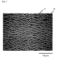
- the random network structure is observed as a structure in such a random state that a shape and a size of an area surrounded by the conductive portion, in which the conductive portion is not present, are irregular when the conductive film is observed with a scanning electron microscope (hereinafter, abbreviated as "SEM"). Therefore, the shape of the conductive portion is observed as a shape in an irregular state.
- SEM scanning electron microscope
- FIG. 1 shows an example of a SEM observation image of a conductive portion consisting of a conductive portion of a random network structure and a base film. It can be said that this configuration is similar to the surface of a muskmelon.
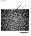
- straight lines in the lower right-hand corner of the drawings are scales, and for example in Figure 1, the length of the straight line in the lower right-hand corner represents 10 ⁇ m.
- a width of the conductive portion of the present invention needs to be 30 ⁇ m or less.
- a line width of the conductive portion may be constant or may vary, and for example, in Figure 1, the conductive portion is observed as a mesh having line widths varying from about 0.3 ⁇ m to about 1 ⁇ m. In the present invention, this width is usually at least 0.2 ⁇ m, and 0.5 to 25 ⁇ m, and preferably 1 to 20 ⁇ m.
- the width of the conductive portion is too small, electrical conductivity is hardly exhibited, and on the other hand, when it is too large, a total light transmittance is apt to decrease in the case of using the conductive film as an electromagnetic interference film and the conductive film is readily observed.
- the conductive portion of the network structure is continuous.
- this can be distinguished through from that the electrical conductivity of the surface is not exhibited.
- an area of portions where the conductive portion is not present is 50% or more with respect to an area of the conductive film, and this area is preferably 60% or more, and more preferably 70% or more particularly from the viewpoint of transparency.
- an upper limit of the percentage of this area may be less than 100%, but it becomes 90% or less in actual production and use.
- the electrical conductivity of the surface of the conductive film of the present invention is not particularly limited as long as an electromagnetic interference function can be attained, but, for example, it is preferably 1 ⁇ 10 5 ⁇ / ⁇ or less, more preferably 1 ⁇ 10 3 ⁇ / ⁇ or less, and most preferably 1 ⁇ / ⁇ or less. Further, the electrical conductivity to be used is preferably 0.1 ⁇ / ⁇ or less in the case of shielding an electromagnetic wave emitted from a PDP television, and the like.
- a higher transmittance of the conductive film of the present invention is preferable, and it is preferably 55% or more, and more preferably 60% or more.
- a ratio of a major axis length to a minor axis length of an area (hereinafter, referred to as a "open area") surrounded by the network of the conductive portion, in which the base film is exposed, is important.
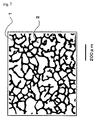
- the major axis length and the minor axis length are determined by following procedure using Figure 3.
- the longest location of an open area surrounded by a watched conductive portion 1 is defined as a major axis A.
- the length of this location is taken as a major axis length.
- two straight lines (B1, B2) in parallel with the defined major axis the two straight lines are placed so that they circumscribe the open area and a distance between them becomes maximum, and a distance C between these straight lines is taken as a minor axis length.
- the average ratios of the major axis length to the minor axis length needs to be larger than 1 and be equal to or less than 3.5.
- the ratio is 1, a problem that the regularity of the network portion is enhanced and a moiré phenomenon tends to occur.
- the ratio is larger than 3.5, there is a problem that anisotropy in images occurs particularly when the conductive film is used in front of an optical illuminant device such as a PDP television.
- a preferable ratio of the major axis length to the minor axis length is 1.2 or more, and furthermore 1.5 or more for a lower value, and 3 or less, further 2.5 or less, and furthermore 1.8 or less for an upper value.
- the conductive portion of the conductive film of the present invention can be obtained by applying a coating solution containing either a material containing a conductive component or a material to have electrical conductivity through a subsequent operation onto the surface of the film, and drying the coating solution.
- a coating solution containing either a material containing a conductive component or a material to have electrical conductivity through a subsequent operation onto the surface of the film, and drying the coating solution.
- a method in which the coating solution is applied onto the surface of the film and dried between step of stretching in a longitudinal direction and the step of stretching in a width direction and then the dried film is further stretched and heat-treated that is, the so-called in-line coating method can be used.
- a layer applied with the coating solution produces cracks through stretching and a conductive portion of the random network structure can be obtained.
- a conductive polymer and/or a conductive particle is preferable.
- the conductive polymer polythiophene, polyaniline, polypyrrole, and derivatives thereof can be used, and as the conductive particle, particles of indium oxide, tin oxide, zinc oxide, silver, gold, copper, platinum, nickel, zinc and the like can be used.
- polythiophene which is a conductive polymer
- this coating solution can also be suitably employed in the present invention.
- a coating solution furthermore preferably, a solution containing a mixture of polythiophene and/or a polythiophene derivative and polyanion (hereinafter, referred to as a "polythiophene-polyanion mixture”) can be used.
- the above-mentioned polythiophene-polyanion mixture usable in the present invention can be obtained by the step of obtaining a polymer having the following repeat structure: and/or the following repeat structure: by polymerizing a monomer to give polythiophene or a polythiophene derivative in the presence of polyanions.
- R 1 and R 2 each independently represent a hydrogen element; or an aliphatic hydrocarbon group, an alicyclic hydrocarbon group, or an aromatic hydrocarbon group, each having 1 to 12 carbon atoms.
- n represents an integer of 1 to 4.
- polythiophene and/or a polythiophene derivative having a structural formula represented by the second repeat structure is preferably used.
- n 1, that is, poly-3,4-ethylenedioxythiophene, is particularly preferable.
- examples of the polythiophene and/or the polythiophene derivative include compounds having a structure in which substituents are bonded at positions 3 and 4 of a thiophene ring and, furthermore, a compound in which oxygen atoms are bonded to carbon atoms at positions 3 and 4 as described above.
- a compound in which oxygen atoms are bonded to carbon atoms at positions 3 and 4 as described above With respect to compounds in which hydrogen atoms or carbon atoms are directly bonded to the above-described carbon atoms, water may not be readily used as a medium of the coating solution.
- the polyanion compound is an acid polymer which can be a free acid, and is a polymer having a carboxylic acid, a polymer having a sulfonic acid, or the like.
- polymers having a carboxylic acid include polyacrylic acid, polymethacrylic acid, and polymaleic acid.
- polymers having a sulfonic acid include polystyrenesulfonic acid, and polyvinylsulfonic acid.
- the polystyrenesulfonic acid is most preferable from the viewpoint of the electrical conductivity of a conductive portion to be obtained.
- a part of functional groups to give free acids may be in the form of neutralized salts.
- polyanion compounds When these polyanion compounds are added during the step of polymerizing for obtaining polythiophene and/or a polythiophene derivative described above, inherently water-insoluble polythiophene-based compounds are readily dispersed in water or readily dissolved in water. Further, it is believed that the function as an acid serves the function as a dopant of the polythiophene-based compound and also serves an effect of improving the electrical conductivity.
- copolymers formed by copolymerization of other copolymerizable monomers e.g., acrylates, methacrylates, and styrene, can also be used.
- the molecular weights of the polyanion compounds such as a carboxylic acid-containing polymer and a sulfonic acid-containing polymer are not specifically limited, but, the weight average molecular weight thereof is preferably 1,000 to 1,000,000, and more preferably 5,000 to 150,000 from the viewpoint of the stability of the coating solution and the conductive portion.
- a part of anions may be neutralized by or may form salts with alkali metals such as lithium, sodium and the like, alkaline earth metals such as calcium and the like, and ammonium ion, to the extent that the characteristic properties of the present invention are not impaired.
- the polyanion is allowed to excessively present with respect to the total amount of the polythiophene and the polythiophene derivative on a weight of solid basis.
- the polyanion is more than 1 part by weight and is equal to or less than 5 parts by weight with respect to 1 part by weight of the total of the polythiophene and the polythiophene derivative, and more preferably is more than 1 part by weight and is equal to or less than 3 parts by weight.
- the polythiophene-polyanion mixture can be produced by methods described in, for example, Japanese Unexamined Patent Publication No. 2000-6324 , European Patent No. 602713 , U.S. Patent No. 5391472 , and the like, although methods other than them may be adopted.
- 3,4-ethylenedioxythiophene is prepared using an alkali metal salt of 3,4-dihydroxythiophene-2,5-dicarboxyester as a starting material. Thereafter, potassium peroxodisulfate, iron sulfate, and 3,4-ethylenedioxythiophene prepared in advance are introduced into and reacted with a polystyrenesulfonic acid aqueous solution, so that a composition can be prepared, in which a polyanion such as polystyrenesulfonic acid forms a complex with a polythiophene such as poly (3,4-ethylenedioxythiophene).
- the random network structure can be formed effectively.
- a resin such as a polyester resin, an urethane resin, an acrylic resin or an epoxy cross-linking agent other than the above-mentioned polythiophene-polyanion mixture in the polythiophene-polyanion mixture in the coating solution.
- the polythiophene-polyanion mixture when only the polythiophene-polyanion mixture is used as a solute, the polythiophene has few follow-up properties to stretching of the base material, and therefore the occurrence of cracks becomes marked, and the conductive portion tends to be independent and the network structure is hardly formed as a conductive portion. Naturally, the electrical conductivity of the film is hardly exhibited.
- the network structure is not formed.
- the content of the polythiophene-polyanion mixture in the solute in the coating solution usually to 8 to 50 percent by weight, preferably to 10 to 50 percent by weight, and more preferably to 12 to 25 percent by weight
- the content of the resin other than the polythiophene-polyanion mixture usually to 50 to 92 percent by weight, preferably to 50 to 90 percent by weight, and more preferably to 75 to 88 percent by weight
- polyester resins contained in the coating solution include polymers or copolymers formed by using acid components selected from terephthalic acid, isophthalic acid, sebacic acid, and 5-sodium sulfoisophthalic acid and/or diol components selected fromethylene glycol, diethylene glycol, 1,4-butanediol, and neopentyl glycol.
- acid components selected from terephthalic acid, isophthalic acid, sebacic acid, and 5-sodium sulfoisophthalic acid and/or diol components selected fromethylene glycol, diethylene glycol, 1,4-butanediol, and neopentyl glycol.
- copolymers in which trimellitic acid is used as a copolymer component in place of 5-sodium sulfoisophthalic acid may also be suitably used.
- the glass transition temperature (hereinafter, abbreviated as "Tg") of the polyester resin is 0°C to 130°C, and more preferably is 10°C to 85°C. If the Tg is lower than 0°C, for example, a blocking phenomenon may occur, in which in winding up a conductive filmprovided with a conductive portion, the conductive portion is adhered to the base film when the conductive portion is provided on only the one side of the film and conductive portions are mutually adhered when the conductive portion is provided on both sides of the film. When the Tg is extremely high, it is undesirable since the stability and the dispersibility in water of the resin may become poor.
- An amount of the polyester resin to be added is preferably 10 to 50 percent by weight in the solute of the coating solution, and more preferably 17 to 34 percent by weight.
- an epoxy-based cross-linking agent suitably added to the coating solution for example, agents of sorbitol polyglycidyl ether-based, polyglycerol polyglycidylether-based, diglycerol polyglycidyl ether-based, polyethylene glycol diglycidyl ether-based, or the like may be used.
- suitable cross-linking agents may include an epoxy compound "DENACOL” (EX-611, EX-614, EX--614B, EX-512, EX-521, EX-421, EX-313, EX-810, EX-830, EX--850, etc.) produced by Nagase ChemteX Corporation, diepoxy and polyepoxy-based compounds (SR-EG, SR-8EG, SR-GLG, etc.) produced by SAKAMOTO YAKUHIN KOGYO CO., LTD., an epoxy cross-linking agent "EPICLON” EM-85--75W or CR-5L produced by DAINIPPON INK AND CHEMICALS, INCORPORATED. Among them, water-soluble cross-linking agents are preferable. An amount of the epoxy-based cross-linking agent to be added is preferably 25 to 75 percent by weight, and more preferably 30 to 60 percent by weight in the solute of the coating solution.
- additives such as antioxidants, heat stabilizers, weathering stabilizers, ultraviolet absorbers, organic lubricants, pigments, dyes, organic or inorganic fine particles, fillers, nucleating agents and the like may also be blended in the solute of the coating solution within the range of not detracting the effects of the present invention.
- a reverse coating method for example, a spray coating method, a bar coating method, a gravure coating method, a rod coating method, and a die coating method can be used.
- the thickness of the conductive portion prepared from this coating solution is not particularly limited, but preferably, it is usually in a range of 0.01 to 5 ⁇ m, and more preferably in a range of 0.02 to 2 ⁇ m. If the thickness of the conductive portion is too small, the electrical conductivity may become poor.
- the film provided with the conductive portion can be prepared by the step (in-line coating method) in which a melt-extruded polyester film before crystalline orientation is done is stretched by about 2.5 to 5 times in a longitudinal direction, and a coating solution is continuously applied to the resulting monoaxially oriented film, and the film coated with the coating solution is dried while being passed through a stepwise-heated zone and stretched by about 2.5 to 5 times in a width direction, and furthermore, the resulting film is continuously led to a heating zone at 150°C to 250°C, and crystalline orientation is completed.
- the coating solution used in this case is preferably a water-based coating solution from the viewpoints of environmental pollution and an explosion-protective property.
- the surface of a base film is subjected to a corona discharge treatment and the like so that the wetting tension of the base film surface is preferably at least 47 mN/m, and more preferably at least 50 mN/m because the adhesion of the conductive portion to the base film can be improved.
- a method of subjecting the monoaxially oriented film to a treatment for improving the wetting tension may be employed.
- a small amount of organic solvent such as isopropyl alcohol, butyl cellosolve, or N-methyl-2-pyrrolidone is contained in the coating solution and, thereby, the wettability and the adhesion to the base film are improved.
- PET polyethylene terephthalate
- PET pellets having an intrinsic viscosity of 0.5 to 0.8 dl/g are vacuum-dried and then are supplied to an extruder.
- the pellets are melted at 260°C to 300°C, and are extruded from a T-die into the form of a sheet.
- the resulting sheet is wound around a mirror-finished casting drum having a surface temperature of 10°C to 60°C by the use of an electrostatic casting method, followed by cooling and solidifying, so that an unstretched PET film is prepared.
- This unstretched film is stretched by 2.5 to 5 times in a longitudinal direction (film traveling direction) between rolls heated to 70°C to 120°C.
- At least one surface of this film is subjected to a corona discharge treatment so that the wetting tension of the surface is at least 47mN/m, and the water-based coating solution that becomes a conductive portion is applied to the treated surface.
- This coated film is grasped with clips, and is led to a hot-air zone heated to 70°C to 150°C to be dried.
- the film is further stretched by 2.5 to 5 times in a width direction, and subsequently, is led to a heat treatment zone at 160°C to 250°C.
- a heat treatment is performed for 1 to 30 seconds, so that crystalline orientation is completed.
- a treatment for relaxation of 1 to 10 percent in a width direction or a longitudinal direction may be performed as required during this heat treatment step.
- this film as a electromagnetic interference film used in flat panel displays such as a plasma display panel and a liquid crystal television by providing a metal layer such as a copper layer on the network structure prepared from the above-mentioned coating solution to form a conductive portion consisting of a layer composed of a coating solution and a metal layer.
- electrolytic copper plating directly to a conductive film having a conductive portion prepared from the above-mentioned coating solution.
- a nucleic agent for nonelectrolytic plating such as palladium is deposited on the conductive film having a conductive portion prepared from the above-mentioned coating solution, and then nonelectrolytic nickel plating or nonelectrolytic copper plating is applied.
- a catalyst for nonelectrolytic plating for example, metal fine particles such as a copper fine particle, a palladium fine particle and a silver fine particle, is mixed in the coating solution for forming a conductive portion in advance, and thereafter a conductive portion of the network structure is formed on a base film and nonelectrolytic plating is applied directly to the resulting conductive film to obtain a metal layer.
- the method described last is useful because number of processes is small.
- a size of the metal fine particle which can be used at this time is not particularly limited, but a number average particle diameter of 0.001 to 1 ⁇ m is preferable. When the number average particle diameter of the metal fine particles exceeds this range, the metal layer may be hardly formed in the form of a network.
- the number average particle diameter of the metal fine particles is 0. 001 to 0.5 ⁇ m, and more preferably 0. 002 to 0.1 ⁇ m.
- a particle diameter of the metal fine particle contained in a metal fine particle layer may be large or small and may be irregular or uniform.
- Metal used for the metal fine particle is not particularly limited and platinum, gold, silver, copper, nickel, palladium, rhodium, ruthenium, bismuth, cobalt, iron, aluminum, zinc, and tin can be used, but particularly, palladium, silver, and copper, which become a catalyst of nonelectrolytic plating, can be suitably used. In addition, these metal may be used singly or in combination of two or more kinds.
- Examples of methods of preparing metal fine particles include a chemical method in which a metal ion is reduced in a liquid layer to form a metal atom and the metal atom is grown to a nanoparticle through a atomic cluster, a technique in which a bulk metals is vaporized in an inert gas to form metal fine particles and these metal fine particles is collected with a cold trap, and a physical method in which a metal thin film obtained by vacuum deposition on a polymer thin film is heated to break the metal thin film and nanoparticles of broken metal is dispersed in a polymer in a solid state.
- Methods for measuring characteristic properties and method for evaluating effects of the present invention are as described below.
- the thickness was determined from the cross-sectional photograph
- the surface of a film was observed with a scanning electron microscope (S-2100A type Hitachi Scanning Electron Microscope, manufactured by Hitachi, Ltd.), and a ratio of a maj or axis length to a minor axis length of an area (open area) surrounded by the network of the conductive portion, in which the base film was exposed, a configuration of the network structure, and a width of the network structure were observed. Further, in the above observation, a magnification of the observation image was adjusted in such a way that the number of open areas was 10 or more.
- the ratio of a major axis length to a minor axis length was determined by measuring all of open areas in a region observed and averaging the measurements. However, the open area, a part of which was out of a field of view and the shape of which could not be identified in the region, was excluded from calculation of this ratio.
- the electrical conductivity was measured based on the surface resistivity.
- a sample was left standing for 24 hours at normal conditions (23°C, relative humidity 65 percent) and, in that atmosphere, the surface resistivity was measured with LORESTA-EP (manufactured by Mitsubishi Chemical Corporation, Model: MCP-T360) according to JIS K 7194.
- Measuring unit is ⁇ / ⁇ .
- This apparatus can measure in a range of 1 ⁇ 10 6 ⁇ / ⁇ or less.
- a measuring range is 1 ⁇ 10 6 ⁇ / ⁇ or more
- the surface resistivity was measured with a digital super-high resistance/microammeter R8340A (manufactured by ADVANTEST CORPORATION).
- the unit is ⁇ / ⁇ .
- the transparency was evaluated by the haze and the total light transmittance.
- a film was left standing for 2 hours at normal conditions (23°C, relative humidity 65 percent), and then the haze and the total light transmittance were measured with a fully automatic direct-reading Haze Computer "HGM-2DP" manufactured by SUGA TEST INSTRUMENTS Co., Ltd. An average value of 3 measurements was taken as the haze value and the total light transmittance of the sample.
- the film was placed in such a way that light enters from the surface on which the conductive portion was provided to be measured.
- a solution in which metal fine particles are dispersed was applied onto a copper mesh and this mesh was observed with a transmission electron microscope (H-7100FA, manufactured by Hitachi, Ltd.) to determine a number average particle diameter of metal fine particles. Particle diameters of 100 metal fine particles were measured and an average thereof was taken as a number average particle diameter.
- the conductive film of the present invention or the electromagnetic interference film was held just anterior to a flat panel display screen on which a image is displayed in such a way that the screen and the film are in parallel with each other, and a substrate was rotated by 360° angle while maintaining a state in which the screen and the film surface are in parallel with each other, and the occurrence of the moiré phenomenon during this rotation was visually checked to evaluate the anti-a moiré phenomenon.
- the evaluations were performed using a liquid crystal display "E152FPb" manufactured by Dell Inc. as a flat pane display.
- the following coating solution for forming a conductive portion was prepared.
- PET pellets (an intrinsic viscosity 0.65 dl/g) were adequately vacuum-dried and then were supplied to an extruder. The pellets were melted at a temperature of 285°C, and were extruded from a T-die into the form of a sheet. The resulting sheet was wound around a mirror-finished casting drum having a surface temperature of 25°C by the use of an electrostatic casting method, followed by cooling and solidifying.
- the unstretched film thus prepared was heated to 89°C, and was stretched by 3.3 times in a longitudinal direction, so that a monoaxially oriented film was prepared. This monoaxially oriented film was subjected to a corona discharge treatment in air in order that the wetting tension of the film became 55mN/m.
- a coating solution for forming a conductive portion described below was applied to the treated surface.
- the monoaxially oriented f ilmto which the coating solution was applied was grasped with clips, and was led to a preheating zone. After drying was performed at a temperature of 95°C, the film was subsequently continuously stretched by 4.0 times in a width direction in a heating zone at a temperature of 110°C, and furthermore, was subjected to a heat treatment in a heating zone at a temperature of 230°C, so that a PET film provided with a conductive portion was prepared, wherein crystalline orientation was completed.
- the thickness of the obtained PET film was 100 ⁇ m, and the thickness of the conductive portion was 0.02 ⁇ m on average.
- Table 1 Excellent transparency and electrical conductivity were exhibited. A moiré phenomenon did not arise.
- a scanning electron microscope (SEM) observation image (magnification of 3000 times) of the conductive film having a conductive portion of a random network structure in the present Example is shown in Figure 4.
- a PET film provided with a conductive portion was prepared by the same procedure as in Example 1 except that a coating solution for forming a conductive portion described below was used in place of the coating solution for forming a conductive portion used in Example 1.
- Table 1 Excellent transparency and electrical conductivity were exhibited. A moiré phenomenon did not arise.
- a PET film provided with a conductive portion was prepared by the same procedure as in Example 1 except that a coating solution for forming a conductive portion described below was used in place of the coating solution for forming a conductive portion used in Example 1.
- a PET film provided with a conductive portion was prepared by the same procedure as in Example 1 except that a coating solution for forming a conductive portion described below was used in place of the coating solution for forming a conductive portion used in Example 1.
- a PET film provided with a conductive portion was prepared by the same procedure as in Example 1 example that a coating solution for forming a conductive portion described below was used in place of the coating solution for forming a conductive portion used in Example 1.
- silver bromide powder (produced by Wako Pure Chemical Industries, Ltd.) was ground for 1 hour with a mortar to obtain more fine powder and this more fine powder was dispersed in an aqueous solution of a nonionic surfactant "OLFINE" EXP-4051F (produced by Nissin Chemical Industry Co., Ltd.) with a homogenizer to obtain a dispersion.
- the obtained conductive film having a conductive portion of a random network structure was subjected to an ultraviolet irradiation treatment (wattage of a lamp 120W, a line speed 1 m/min, irradiation intensity 1000 mJ/cm 2 , the number of irradiation twice) and was exposed, and then the exposed film was developed and fixed using a commercially available developing solution (“FUJIDOL” E (for monochrome photographs) produced by FUJIFILM Corporation) and a commercially available fixing solution (“FUJIFIX” (for monochrome films) produced by FUJIFILM Corporation).
- Thefollowing nonelectrolytic copper plating was carried out using silver produced in the network structure as a catalyst.
- Plating solution "MELPLATE” CU-5100 produced by Meltex Inc. Temperature in plating: 50°C Plating time: 3 minutes
- a conductive portion consisting of a layer formed from a coating solution and a metal layer could be prepared by providing metal copper layer on the conductive portion formed from the coating solution for a conductive film.
- the results are shown in Table 2. Excellent transparency and electrical conductivity were exhibited. A moiré phenomenon did not arise.
- Monoethanolamine was added dropwise to an aqueous solution of silver nitrate to obtain an aqueous solution of silver alkanolamine complex (aqueous solution 1).
- an aqueous solution formed by adding monoethanolamine to an aqueous solution in which quinine was dissolved as a reducing agent was prepared.
- the aqueous solution 1 and the aqueous solution 2 were simultaneously poured into a plastic container and the silver alkanolamine complex was reduced to silver fine particles.
- This mixture solution was filtrated, washed with water and dried to obtain silver fine particles. Further, these silver fine particles were re-dispersed in water to obtain a silver fine particle dispersion. Number average particle diameter of silver fine particles was 1.4 ⁇ m.
- a coated film in which a layer of a silver fine particle was laminated in the form of random network was obtained by printing the silver fine particle solution prepared in (Synthetic Example 1) in a random network structure shown in Figure 3 on one side of a biaxially oriented polyethylene terephthalate film ("Lumirror" U94 produced by Toray Industries, Inc.) by screen printing and drying the printed solution at 120°C for 1 minute. The thickness of the network structure was adjusted to 2 ⁇ m. The layer of a silver fine particle of this coated film was immersed in 0.1 N hydrochloric acid (N/10 hydrochloric acid produced by NACALAI TESQUE, Inc.) for 2 minutes. Then, after the coated film was taken out and washed with water, it was dried at 120°C for 1 minute.
- N hydrochloric acid N/10 hydrochloric acid produced by NACALAI TESQUE, Inc.
- Example 5 The nonelectrolytic copper plating described in Example 5 was applied to the coated film prepared in Example 6 for 20 minutes. The results are shown in Table 2. Excellent transparency and electrical conductivity were exhibited. A moiré phenomenon did not arise.
- a coated film in which a layer of a silver fine particle was provided in the form of grid was obtained by printing the silver fine particle solution prepared in Synthetic Example 1 in the form of grid having a line thickness of 3 ⁇ m, a line width of 35 ⁇ m, and a pitch of 300 ⁇ m on one side of a biaxially oriented polyethylene terephthalate film ("Lumirror" U94 produced by Toray Industries, Inc.) by screen printing and drying the printed solution at 120°C for 1 minute. The results are shown in Table 2. This coated film is low in electrical conductivity and produced a moiré phenomenon.
- Example 6 The nonelectrolytic plating was performed for 40 minutes in Example 6. The results are shown in Table 2. This film was extremely low in the transparency.
- Example 6 a conductive film having a conductive portion of 3 ⁇ m in thickness having the network structure was obtained by printing conductive thermosetting silver paste (produced by TOYOBO CO., LTD., conductive thermosetting silver paste DW-250H-5) in a random network structure described above on one side of a biaxially oriented polyethylene terephthalate film ("Lumirror" U94 produced by Toray Industries, Inc.) by screen printing and drying the printed solution at 130°C for 30 minutes.
- Limirror biaxially oriented polyethylene terephthalate film
- a PET film was prepared by the same procedure as in Example 1 except that a coating solution for forming a conductive portion described below was used in place of the coating solution for forming a conductive portion used in Example 1.
- a coating solution for forming a conductive portion was prepared by using only the above-mentioned coating solution A1. That is, a resin other than the polythiophene-polyanion mixture is not mixed. The results are shown in Table 2. This film was extremely low in the transparency and electrical conductivity, and exhibited remarkable occurrences of cracks and strong anisotropy such that the brightness varied depending on viewing angle.
- Example 1 Composition of Coating solution for conductive portion Line width ( ⁇ m) Haze (%) Total light transmittance (%) Electrical conductivity ( ⁇ / ⁇ ) Aperture ratio (%) Ratio of major axis length to minor axis length Moiré Type Ratio on weight of solid basis Minimum Maximum Example 1 A1/B1/C1 16/34/50 0.2 1.1 3.7 88 4 ⁇ 10 4 60 1.8 Not arise Example 2 A1/B1/C1 8/17/75 0.2 1 2.8 89 8 ⁇ 10 4 55 1.7 Not arise Example 3 A1/B1/C1 25/50/25 0.4 2 4.2 88 1 ⁇ 10 4 65 2.5 Not arise Example 4 A1/B2/C2 16/34/50 0.2 1.1 3 89 1 ⁇ 10 4 60 1.8 Not arise Table 2 Constitution of network structure Line width ( ⁇ m) Haze (%) Total light transmittance (%) Electrical conductivity ( ⁇ / ⁇ ) Aperture ratio (%) Ratio of major axis length to minor axis length Moiré Minimum Maximum Example 5 Conductive layer of Example 1 containing silver
- the conductive film of the present invention has a random network structure and has transparency and a high level of electrical conductivity. Therefore, by providing a metal layer such as a copper layer on the random network structure, the conductive film of the present invention is useful as an electromagnetic interference film hardly causing a moiré phenomenon, which is suitably used for flat panel displays such as a plasma display panel and a liquid crystal television.
Landscapes
- Engineering & Computer Science (AREA)
- Physics & Mathematics (AREA)
- Microelectronics & Electronic Packaging (AREA)
- Textile Engineering (AREA)
- Electromagnetism (AREA)
- Plasma & Fusion (AREA)
- Laminated Bodies (AREA)
- Shielding Devices Or Components To Electric Or Magnetic Fields (AREA)
- Non-Insulated Conductors (AREA)
Abstract
The present invention aims at providing a conductive film having transparency and a high level of electrical conductivity, which is used for an electromagnetic interference film hardly causing a moiré phenomenon, and the like. To achieve the above-mentioned aim, the following invention is disclosed. A conductive film in which a conductive portion of a random network structure is present on at least one surface of a base film, a line width of the conductive portion composing the network structure is 30 µm or less, an area of portions where the conductive portion is not present is 50% or more with respect to an area of the conductive film, and an average of ratios of a major axis length to a minor axis length of an area surrounded by the network of the conductive portion, in which the base film is exposed, is larger than 1 and is equal to or less than 3.5.
Description
- The present invention relates to a conductive film which is suitable for an electromagnetic interference film capable of being used for flat panel displays such as a plasma display panel and a liquid crystal television.
- Generally, a variety of electromagnetic waves are emitted from electronic equipment including household electrical appliances, mobile phones, personal computers, and televisions. A strong electromagnetic wave is also emitted from flat panel displays such as a plasma display panel and a liquid crystal television among significantly increasing digital household electrical appliances, and its influence on the human health is also concerned. People observe the images of such displays within a distance relatively close to these displays and for long time in some cases. By doing so, an electromagnetic interference film suppressing these electromagnetic waves is required and the development thereof has been intensively investigated.
- In electromagnetic interference films known at present, various methods for suppressing these electromagnetic waves are adopted. For example, a method, in which copper foil is bonded to a polyester film, a regular mesh shape is patterned by photolithography, and etching is performed in such a way that the copper foil becomes a network configuration to prepare a conductive film in which a conductive portion is made from copper and has a network structure, is disclosed in
Patent document 1. - As another method, a method of fabricating a conductive film by printing a composition containing a nucleic agent for plating such as palladium on a film such as polyester in a regular form of network by a printing method and further by applying nonelectrolytic copper plating to a layer consisting of the composition in the form of network is disclosed in
Patent document 2. - As further method, a method of fabricating a conductive film by bonding a knit of metal fiber woven in length and width onto a polyester film or the like is disclosed in Patent document 3.
- Further, a conductive body in the form of network which is obtained by initiating micro-cracks in the random form of network and by filling the micro-cracks with a conductive material is disclosed in Patent Document 4, a transparent conductive film provided with a layer in which metal fine particles coagulate in the random form of network is disclosed in Patent document 5, transparent conductive film provided with a layer containing silver colloidal particles is disclosed in Patent document 6, and a transparent conductive layer having a fine network structure using silver is disclosed in Patent document 7.
- Patent Document 1:
Japanese Unexamined Patent Publication No.2001-210988 page 1, claims etc.) - Patent Document 2:
Japanese Unexamined Patent Publication No.2002-185184 page 1, claims etc.) - Patent Document 3:
Japanese Unexamined Patent Publication No.11-119672 page 1, claims etc.) - Patent Document 4:
Japanese Unexamined Patent Publication No.2004-228057 page 1, claims etc.) - Patent Document 5:
Japanese Unexamined Patent Publication No.2003-71976 page 1, claims etc.) - Patent Document 6:
Japanese Unexamined Patent Publication No.2001-60416 page 1, claims etc.) - Patent Document 7:
Japanese Unexamined Patent Publication No.10-312715 page 1, claims etc.) - However, there are the following problems in the prior art described above.
- A method for etching copper foil is an excellent method for attaining a highly precise network structure, but it is generally low in yields in the steps of bonding copper foil, photolithography, and etching and consequently the yield of a final product becomes low. Further, since a hazardous waste fluid is produced in the etching step, safety and environmental precautions are required. Further, when the copper foil is used as a material, there is also a problem that much of the copper foil is eluted through etching to generate a waste fluid and therefore an amount of a material to be recovered is large.
- A method of producing a conductive film by a nonelectrolytic plating process has a feature that an amount of metal waste fluid to be treated is small since metal is used for only required portion. But, since it is difficult to form a pattern of more fine line in the step of printing a mesh form, which is a first step, it is consequently difficult to obtain a conductive film having a conductive portion of a fine line.
- A method of bonding metal fiber is a very simple method and readily attains the effect of shielding an electromagnetic wave, but it has a problem that it is difficult to make the network of a conductive portion fine.
- The other large problem in technologies described above is a moiré phenomenon occurring when the conductive film is used as an electromagnetic interference film at the surface of a display. The moiré phenomenon is a phenomenon of a fleck pattern in stripe form generated when patterns in which dots or lines are geometrically regularly distributed are superimposed. As for the flat panel display, a moiré in stripe form tends to arise on a screen. This moiré phenomenon arises by an interaction between the pattern of display devices of respective RGB colors of a displaymain body and the regular configuration of the network of the electromagnetic interference film placed in front of the display main body. These are arrayed regularly to each other, and particularly the display device cannot be changed from a regular configuration to an irregular configuration.
- It is an object of the present invention to solve the above-mentioned problems and to provide an excellent conductive film which is easy to produce and hardly causes a moiré phenomenon when it is applied to flat panel displays as an electromagnetic interference film.
- In order to solve the above-mentionedproblems, the present invention has the following constitutions.
- (1) A conductive film in which a conductive portion of a random network structure is present on at least one surface of a base film, a line width of the conductive portion composing the network structure is 30 µm or less, an area of portions where the conductive portion is not present is 50% or more with respect to an area of the conductive film, and an average of ratios of a major axis length to a minor axis length of an area surrounded by the network of the conductive portion, in which the base film is exposed, is larger than 1 and is equal to or less than 3.5.
- (2) The conductive film according to the above (1), wherein the conductive portion of a random network structure is obtained by the steps of applying a solution for forming a conductive portion to the base film and drying the solution.
- (3) The conductive film according to any one of the above, wherein the conductive portion contains a conductive polymer and/or a conductive particle.
- (4) The conductive film according to any one of the above, wherein the conductive portion of the conductive film includes a layer containing a conductive polymer and/or a conductive particle, and a metal layer provided on the layer.
- (5) The conductive film according to any one of the above, wherein the prime constituent of metal to form the metal layer is copper.
- (6) The conductive film according to any one of the above, wherein the conductive film is an electromagnetic interference film.
- In accordance with the present invention, it is possible to provide a conductive film having transparency and a high level of electrical conductivity as well as less moirés, and further it is possible to provide an excellent electromagnetic interference film hardly causing a moiré phenomenon when a metal layer is provided on its conductive portion. This conductive film is very useful for flat panel displays such as a plasma display panel and a liquid crystal television.
-
- Figure 1 is a scanning electron microscope observation image showing an example of a random network structure according to the present invention,
- Figure 2 is a scanning electron microscope observation image showing an example of a random network structure according to the present invention,
- Figure 3 is a view showing a method for determining a major axis length and a minor axis length,
- Figure 4 is a scanning electron microscope observation image showing a random network structure in Example 1, and
- Figure 5 is a scanning electron microscope observation image showing a random network structure in Comparative Example 3.
-
- 1: conductive portion
- 2 : area where a base film is exposed, having no conductive portion on it
- A conductive film of the present invention is a conductive film in which a conductive portion of a random network structure is present on at least one surface of a base film, a line width of the conductive portion composing the network structure is 30 µm or less, an area of portions where the conductive portion is not present is 50% or more with respect to an area of the conductive film, and an average of ratios of a major axis length to a minor axis length of an area surrounded by the network of the conductive portion, in which the base film is exposed, is larger than 1 and is equal to or less than 3.5.
- The base film used in the present invention is preferably a film composed of a resin. Preferably, the resin is further a thermoplastic resin. The thermoplastic resin film collectively refers to films which are melted or softened by heating. The thermoplastic resin film is not particularly limited, and typical examples of thermoplastic resin films to be used may include polyester films; polyolefin films such as polypropylene films and polyethylene films; polylactic acid films; polycarbonate films; acrylic films such as polymethyl methacrylate films and polystyrene films; polyamide films such as nylon; polyvinyl chloride films; polyurethane films; fluorine-based films; and polyphenylene sulfide films.
- A resin composing the base film may be homopolymers or copolymers. Among them, polyester films, polypropylene films, polyamide films, and the like are preferable from the viewpoint of mechanical properties, the dimensional stability, the transparency, and the like, and furthermore, polyester films are preferable from the viewpoint of the mechanical strength, the general versatility, and the like.
- These films may contain various additives, e.g., antioxidants, heat stabilizers, weathering stabilizers, ultraviolet absorbers, organic lubricants, pigments, dyes, organic or inorganic fine particles, fillers, antistatic agents and crystal nucleating agents, to the extent that the characteristic properties are not deteriorated.
- The thickness of the base film is not specifically limited, and is appropriately selected in accordance with the applications and the kinds of the conductive film of the present invention. Preferably, the thickness is usually 10 to 500 µm, more preferably is 38 to 250 µm, and most preferably is 75 to 150 µm from the viewpoint of the mechanical strength, handleability, and the like.
- The example in which a polyester film is used as a base film of the conductive film of the present invention will be described below.
- A polyester composing a polyester film refers to polymers in which ester bonding is a primary bonding chain in a main chain. As the polyester, polyethylene terephthalate, polypropylene terephthalate, ethylene-2,6-naphthalate, polybutylene terephthalate, polypropylene-2,6-naphthalate, polyethylene-α,β-bis (2-chlorophenoxy)ethane-4,4'-dicarboxylate, and the like are exemplified, and polyesters including at least one constituent selected from the group consisting of the above-mentioned polymers as a primary constituent can be preferably used.
- These constituents may be used alone or in combination of two or more kinds. Most of all, it is particularly preferable to use polyethylene terephthalate, considering collectively all the factors, e.g., quality and economy, involved. When the conductive film is used for the case where there is a step of performing intensive heat treatment or tending to produce shrinkage stress, polyethylene-2,6-naphthalate having excellent heat resistance and stiffness is also suitably used. Other dicarboxylic acid components and/or idol components may be copolymerized as a part of two polyesters exemplified here, preferably at 20 mole percent or less. Also, hydroxyl carboxylic acid components may be copolymerized.
- It is suitable for performing the present invention that the intrinsic viscosity (measured in o-chlorophenol at 25°C) of the above-described polyester is preferably within the range of 0.4 to 1.2 dl/g, and more preferably within the range of 0. 5 to 0.8 dl/g.
- Preferably, the polyester film of a base material is biaxially oriented. In general, the biaxially oriented polyester film refers to a polyester film which is prepared by stretching an unstretched polyester sheet or film preferably by about 2.5 to 5 times in each of a longitudinal direction and a width direction, respectively, and then processing the film with a heat treatment to complete crystalline orientation. This film exhibits a wide-angle X-ray diffraction pattern attributed to biaxial orientation.
- A polyester film to be a base film may be a composite film prepared by coextrusion. On the other hand, the resulting films may also be bonded to each other by various methods to be used.
- Next, the conductive portion of a randomnetwork structure, which is present on at least one surface of the base film, will be described.
- The random network structure is observed as a structure in such a random state that a shape and a size of an area surrounded by the conductive portion, in which the conductive portion is not present, are irregular when the conductive film is observed with a scanning electron microscope (hereinafter, abbreviated as "SEM"). Therefore, the shape of the conductive portion is observed as a shape in an irregular state.
- A SEM observation image of the conductive layer formed on a base film of the conductive film of the present invention is shown in Figures 1 and 2. Figure 1 shows an example of a SEM observation image of a conductive portion consisting of a conductive portion of a random network structure and a base film. It can be said that this configuration is similar to the surface of a muskmelon. Here, straight lines in the lower right-hand corner of the drawings are scales, and for example in Figure 1, the length of the straight line in the lower right-hand corner represents 10 µm.
- A width of the conductive portion of the present invention needs to be 30 µm or less. A line width of the conductive portion may be constant or may vary, and for example, in Figure 1, the conductive portion is observed as a mesh having line widths varying from about 0.3 µm to about 1 µm. In the present invention, this width is usually at least 0.2 µm, and 0.5 to 25 µm, and preferably 1 to 20 µm. When the width of the conductive portion is too small, electrical conductivity is hardly exhibited, and on the other hand, when it is too large, a total light transmittance is apt to decrease in the case of using the conductive film as an electromagnetic interference film and the conductive film is readily observed.
- It is preferable that at least a part of the conductive portion of the network structure is continuous. When the conductive portion is not continuous, this can be distinguished through from that the electrical conductivity of the surface is not exhibited.
- In the conductive film of the present invention, it is necessary that an area of portions where the conductive portion is not present is 50% or more with respect to an area of the conductive film, and this area is preferably 60% or more, and more preferably 70% or more particularly from the viewpoint of transparency.
- When the percentage of this area is low, it is not desirable since a total light transmittance is lowered in the case of using the conductive film as an electromagnetic interference film. On the other hand, an upper limit of the percentage of this area may be less than 100%, but it becomes 90% or less in actual production and use.
- The electrical conductivity of the surface of the conductive film of the present invention is not particularly limited as long as an electromagnetic interference function can be attained, but, for example, it is preferably 1×10⁵ Ω/□ or less, more preferably 1×10³ Ω/□ or less, and most preferably 1 Ω/□ or less. Further, the electrical conductivity to be used is preferably 0.1 Ω/□ or less in the case of shielding an electromagnetic wave emitted from a PDP television, and the like.
- A higher transmittance of the conductive film of the present invention is preferable, and it is preferably 55% or more, and more preferably 60% or more.
- Further, in the present invention, a ratio of a major axis length to a minor axis length of an area (hereinafter, referred to as a "open area") surrounded by the network of the conductive portion, in which the base film is exposed, is important. The major axis length and the minor axis length are determined by following procedure using Figure 3.
- The longest location of an open area surrounded by a watched
conductive portion 1 is defined as a major axis A. The length of this location is taken as a major axis length. Assuming two straight lines (B1, B2) in parallel with the defined major axis, the two straight lines are placed so that they circumscribe the open area and a distance between them becomes maximum, and a distance C between these straight lines is taken as a minor axis length. - The average ratios of the major axis length to the minor axis length needs to be larger than 1 and be equal to or less than 3.5. When the ratio is 1, a problem that the regularity of the network portion is enhanced and a moiré phenomenon tends to occur. When, the ratio is larger than 3.5, there is a problem that anisotropy in images occurs particularly when the conductive film is used in front of an optical illuminant device such as a PDP television. A preferable ratio of the major axis length to the minor axis length is 1.2 or more, and furthermore 1.5 or more for a lower value, and 3 or less, further 2.5 or less, and furthermore 1.8 or less for an upper value.
- The conductive portion of the conductive film of the present invention can be obtained by applying a coating solution containing either a material containing a conductive component or a material to have electrical conductivity through a subsequent operation onto the surface of the film, and drying the coating solution. For example, in a manufacturing step of biaxially stretching a polyester film successively in which a step of stretching in a longitudinal direction and a step of stretching in a width direction are performed, a method in which the coating solution is applied onto the surface of the film and dried between step of stretching in a longitudinal direction and the step of stretching in a width direction and then the dried film is further stretched and heat-treated, that is, the so-called in-line coating method can be used. In the step of stretching a film in a width direction, a layer applied with the coating solution produces cracks through stretching and a conductive portion of the random network structure can be obtained.
- As a component contained in the coating solution, a conductive polymer and/or a conductive particle is preferable. As the conductive polymer, polythiophene, polyaniline, polypyrrole, and derivatives thereof can be used, and as the conductive particle, particles of indium oxide, tin oxide, zinc oxide, silver, gold, copper, platinum, nickel, zinc and the like can be used.
- In particular, with respect to polythiophene which is a conductive polymer, the development of a coating solution in which water is used as a medium is advanced by the recent research and development, and this coating solution can also be suitably employed in the present invention. As a coating solution, furthermore preferably, a solution containing a mixture of polythiophene and/or a polythiophene derivative and polyanion (hereinafter, referred to as a "polythiophene-polyanion mixture") can be used.
- The above-mentioned polythiophene-polyanion mixture usable in the present invention can be obtained by the step of obtaining a polymer having the following repeat structure:


- As a material to give the conductive portion of the present invention, polythiophene and/or a polythiophene derivative having a structural formula represented by the second repeat structure is preferably used. For example, a preferable compound is represented by the second repeat structure, where n = 1 (a methylene group), n = 2 (an ethylene group), or n = 3 (a trimethylene group). Among them, a compound including an ethylene group in which n = 2, that is, poly-3,4-ethylenedioxythiophene, is particularly preferable.
- Further, examples of the polythiophene and/or the polythiophene derivative include compounds having a structure in which substituents are bonded at positions 3 and 4 of a thiophene ring and, furthermore, a compound in which oxygen atoms are bonded to carbon atoms at positions 3 and 4 as described above. With respect to compounds in which hydrogen atoms or carbon atoms are directly bonded to the above-described carbon atoms, water may not be readily used as a medium of the coating solution.
- Next, a polyanion compound suitably used for the polythiophene-polyanion mixture will be described.
- The polyanion compound is an acid polymer which can be a free acid, and is a polymer having a carboxylic acid, a polymer having a sulfonic acid, or the like. Examples of polymers having a carboxylic acid include polyacrylic acid, polymethacrylic acid, and polymaleic acid. Examples of polymers having a sulfonic acid include polystyrenesulfonic acid, and polyvinylsulfonic acid. In particular, the polystyrenesulfonic acid is most preferable from the viewpoint of the electrical conductivity of a conductive portion to be obtained. Here, a part of functional groups to give free acids may be in the form of neutralized salts.
- When these polyanion compounds are added during the step of polymerizing for obtaining polythiophene and/or a polythiophene derivative described above, inherently water-insoluble polythiophene-based compounds are readily dispersed in water or readily dissolved in water. Further, it is believed that the function as an acid serves the function as a dopant of the polythiophene-based compound and also serves an effect of improving the electrical conductivity.
- Here, as the polyanion compound described above, copolymers formed by copolymerization of other copolymerizable monomers, e.g., acrylates, methacrylates, and styrene, can also be used.
- The molecular weights of the polyanion compounds such as a carboxylic acid-containing polymer and a sulfonic acid-containing polymer are not specifically limited, but, the weight average molecular weight thereof is preferably 1,000 to 1,000,000, and more preferably 5,000 to 150,000 from the viewpoint of the stability of the coating solution and the conductive portion. A part of anions may be neutralized by or may form salts with alkali metals such as lithium, sodium and the like, alkaline earth metals such as calcium and the like, and ammonium ion, to the extent that the characteristic properties of the present invention are not impaired.
- In the polythiophene-polyanion mixture of the present invention, it is preferable from the viewpoint of the electrical conductivity that the polyanion is allowed to excessively present with respect to the total amount of the polythiophene and the polythiophene derivative on a weight of solid basis. Preferably, the polyanion is more than 1 part by weight and is equal to or less than 5 parts by weight with respect to 1 part by weight of the total of the polythiophene and the polythiophene derivative, and more preferably is more than 1 part by weight and is equal to or less than 3 parts by weight. In addition, the polythiophene-polyanion mixture can be produced by methods described in, for example,
Japanese Unexamined Patent Publication No. 2000-6324 European Patent No. 602713 U.S. Patent No. 5391472 , and the like, although methods other than them may be adopted. - For example, 3,4-ethylenedioxythiophene is prepared using an alkali metal salt of 3,4-dihydroxythiophene-2,5-dicarboxyester as a starting material. Thereafter, potassium peroxodisulfate, iron sulfate, and 3,4-ethylenedioxythiophene prepared in advance are introduced into and reacted with a polystyrenesulfonic acid aqueous solution, so that a composition can be prepared, in which a polyanion such as polystyrenesulfonic acid forms a complex with a polythiophene such as poly (3,4-ethylenedioxythiophene).
- As a water-based coating solution containing poly(3,4-ethylenedioxythiophene) and polystyrenesulfonic acid, a product sold by H.C. Starck Ltd. (German) under the trade name "Baytron" P, or the like can be employed.
- By containing a resin such as a polyester resin, an urethane resin, an acrylic resin or an epoxy cross-linking agent other than the above-mentioned polythiophene-polyanion mixture in the polythiophene-polyanion mixture in the coating solution, the random network structure can be formed effectively. For example, when only the polythiophene-polyanion mixture is used as a solute, the polythiophene has few follow-up properties to stretching of the base material, and therefore the occurrence of cracks becomes marked, and the conductive portion tends to be independent and the network structure is hardly formed as a conductive portion. Naturally, the electrical conductivity of the film is hardly exhibited. On the other hand, when large amounts of these resins are added, the network structure is not formed. By adjusting the content of the polythiophene-polyanion mixture in the solute in the coating solution usually to 8 to 50 percent by weight, preferably to 10 to 50 percent by weight, and more preferably to 12 to 25 percent by weight, and on the other hand, by adjusting the content of the resin other than the polythiophene-polyanion mixture usually to 50 to 92 percent by weight, preferably to 50 to 90 percent by weight, and more preferably to 75 to 88 percent by weight, the random network structure is formed effectively.
- Examples of preferable polyester resins contained in the coating solution include polymers or copolymers formed by using acid components selected from terephthalic acid, isophthalic acid, sebacic acid, and 5-sodium sulfoisophthalic acid and/or diol components selected fromethylene glycol, diethylene glycol, 1,4-butanediol, and neopentyl glycol. In the case where the water resistance is required, copolymers in which trimellitic acid is used as a copolymer component in place of 5-sodium sulfoisophthalic acid may also be suitably used.
- Preferably, the glass transition temperature (hereinafter, abbreviated as "Tg") of the polyester resin is 0°C to 130°C, and more preferably is 10°C to 85°C. If the Tg is lower than 0°C, for example, a blocking phenomenon may occur, in which in winding up a conductive filmprovided with a conductive portion, the conductive portion is adhered to the base film when the conductive portion is provided on only the one side of the film and conductive portions are mutually adhered when the conductive portion is provided on both sides of the film. When the Tg is extremely high, it is undesirable since the stability and the dispersibility in water of the resin may become poor. An amount of the polyester resin to be added is preferably 10 to 50 percent by weight in the solute of the coating solution, and more preferably 17 to 34 percent by weight.
- Further, as an epoxy-based cross-linking agent suitably added to the coating solution, for example, agents of sorbitol polyglycidyl ether-based, polyglycerol polyglycidylether-based, diglycerol polyglycidyl ether-based, polyethylene glycol diglycidyl ether-based, or the like may be used. Examples of suitable cross-linking agents may include an epoxy compound "DENACOL" (EX-611, EX-614, EX--614B, EX-512, EX-521, EX-421, EX-313, EX-810, EX-830, EX--850, etc.) produced by Nagase ChemteX Corporation, diepoxy and polyepoxy-based compounds (SR-EG, SR-8EG, SR-GLG, etc.) produced by SAKAMOTO YAKUHIN KOGYO CO., LTD., an epoxy cross-linking agent "EPICLON" EM-85--75W or CR-5L produced by DAINIPPON INK AND CHEMICALS, INCORPORATED. Among them, water-soluble cross-linking agents are preferable. An amount of the epoxy-based cross-linking agent to be added is preferably 25 to 75 percent by weight, and more preferably 30 to 60 percent by weight in the solute of the coating solution.
- Furthermore, various additives such as antioxidants, heat stabilizers, weathering stabilizers, ultraviolet absorbers, organic lubricants, pigments, dyes, organic or inorganic fine particles, fillers, nucleating agents and the like may also be blended in the solute of the coating solution within the range of not detracting the effects of the present invention.
- As the method for coating the base film with the coating solution, for example, a reverse coating method, a spray coating method, a bar coating method, a gravure coating method, a rod coating method, and a die coating method can be used.
- The thickness of the conductive portion prepared from this coating solution is not particularly limited, but preferably, it is usually in a range of 0.01 to 5 µm, and more preferably in a range of 0.02 to 2 µm. If the thickness of the conductive portion is too small, the electrical conductivity may become poor.
- As a further preferable method for providing the conductive portion, a method in which the coating solution is applied during the step of manufacturing a polyester film and is stretched together with the base film is most suitable. For example, the film provided with the conductive portion can be prepared by the step (in-line coating method) in which a melt-extruded polyester film before crystalline orientation is done is stretched by about 2.5 to 5 times in a longitudinal direction, and a coating solution is continuously applied to the resulting monoaxially oriented film, and the film coated with the coating solution is dried while being passed through a stepwise-heated zone and stretched by about 2.5 to 5 times in a width direction, and furthermore, the resulting film is continuously led to a heating zone at 150°C to 250°C, and crystalline orientation is completed. The coating solution used in this case is preferably a water-based coating solution from the viewpoints of environmental pollution and an explosion-protective property.
- In the present invention, it is preferable that before the coating solution is applied, the surface of a base film is subjected to a corona discharge treatment and the like so that the wetting tension of the base film surface is preferably at least 47 mN/m, and more preferably at least 50 mN/m because the adhesion of the conductive portion to the base film can be improved. Naturally, a method of subjecting the monoaxially oriented film to a treatment for improving the wetting tension may be employed. Further, it is also preferable that a small amount of organic solvent such as isopropyl alcohol, butyl cellosolve, or N-methyl-2-pyrrolidone is contained in the coating solution and, thereby, the wettability and the adhesion to the base film are improved.
- Next, the method for manufacturing a conductive film of the present invention will be described in further detail with reference to the example in which polyethylene terephthalate (hereafter abbreviated as "PET") is used as the base film, although not limited to this.
- The method for manufacturing a conductive film of the present invention will be described with reference to further specific example.
- PET pellets having an intrinsic viscosity of 0.5 to 0.8 dl/g are vacuum-dried and then are supplied to an extruder. The pellets are melted at 260°C to 300°C, and are extruded from a T-die into the form of a sheet. The resulting sheet is wound around a mirror-finished casting drum having a surface temperature of 10°C to 60°C by the use of an electrostatic casting method, followed by cooling and solidifying, so that an unstretched PET film is prepared. This unstretched film is stretched by 2.5 to 5 times in a longitudinal direction (film traveling direction) between rolls heated to 70°C to 120°C. At least one surface of this film is subjected to a corona discharge treatment so that the wetting tension of the surface is at least 47mN/m, and the water-based coating solution that becomes a conductive portion is applied to the treated surface. This coated film is grasped with clips, and is led to a hot-air zone heated to 70°C to 150°C to be dried. The film is further stretched by 2.5 to 5 times in a width direction, and subsequently, is led to a heat treatment zone at 160°C to 250°C. A heat treatment is performed for 1 to 30 seconds, so that crystalline orientation is completed. A treatment for relaxation of 1 to 10 percent in a width direction or a longitudinal direction may be performed as required during this heat treatment step.
- It becomes possible to use this film as a electromagnetic interference film used in flat panel displays such as a plasma display panel and a liquid crystal television by providing a metal layer such as a copper layer on the network structure prepared from the above-mentioned coating solution to form a conductive portion consisting of a layer composed of a coating solution and a metal layer.
- There is, for example, a method for applying electrolytic copper plating directly to a conductive film having a conductive portion prepared from the above-mentioned coating solution. Further, there is a method in which a nucleic agent for nonelectrolytic plating such as palladium is deposited on the conductive film having a conductive portion prepared from the above-mentioned coating solution, and then nonelectrolytic nickel plating or nonelectrolytic copper plating is applied. Further, there is another method in which a method for applying electrolytic copper plating onto the layer obtained by the above-mentioned nonelectrolytic plating is exemplified, a catalyst for nonelectrolytic plating, for example, metal fine particles such as a copper fine particle, a palladium fine particle and a silver fine particle, is mixed in the coating solution for forming a conductive portion in advance, and thereafter a conductive portion of the network structure is formed on a base film and nonelectrolytic plating is applied directly to the resulting conductive film to obtain a metal layer. Particularly, the method described last is useful because number of processes is small.
- A size of the metal fine particle which can be used at this time is not particularly limited, but a number average particle diameter of 0.001 to 1 µm is preferable. When the number average particle diameter of the metal fine particles exceeds this range, the metal layer may be hardly formed in the form of a network. Preferably, the number average particle diameter of the metal fine particles is 0. 001 to 0.5 µm, and more preferably 0. 002 to 0.1 µm. A particle diameter of the metal fine particle contained in a metal fine particle layer may be large or small and may be irregular or uniform. Metal used for the metal fine particle is not particularly limited and platinum, gold, silver, copper, nickel, palladium, rhodium, ruthenium, bismuth, cobalt, iron, aluminum, zinc, and tin can be used, but particularly, palladium, silver, and copper, which become a catalyst of nonelectrolytic plating, can be suitably used. In addition, these metal may be used singly or in combination of two or more kinds.
- Examples of methods of preparing metal fine particles include a chemical method in which a metal ion is reduced in a liquid layer to form a metal atom and the metal atom is grown to a nanoparticle through a atomic cluster, a technique in which a bulk metals is vaporized in an inert gas to form metal fine particles and these metal fine particles is collected with a cold trap, and a physical method in which a metal thin film obtained by vacuum deposition on a polymer thin film is heated to break the metal thin film and nanoparticles of broken metal is dispersed in a polymer in a solid state.
- [Methods for measuring characteristic properties and method for evaluating effects] Methods for measuring characteristic properties and methods for evaluating effects of the present invention are as described below.
- A sample, for example, a cross section of a laminated polyester film, was cut out into a extremely thin slice, and this slice was observed and photographed with a TEM (transmission electron microscope) using a method of an extremely thin slice stained by ruthenic acid (RuO4) or osmic acid (OsO4), or double-stained by both of RuO4 and OsO4. The thickness was determined from the cross-sectional photograph
-
- Apparatus: transmission electron microscope (H-7100FA, manufactured by Hitachi, Ltd.)
- Measuring condition: acceleration voltage 100 kV
- Sample preparation: Extremely thin slice method
- Observation magnification: 20000 times to 200000 times
- The surface of a film was observed with a scanning electron microscope (S-2100A type Hitachi Scanning Electron Microscope, manufactured by Hitachi, Ltd.), and a ratio of a maj or axis length to a minor axis length of an area (open area) surrounded by the network of the conductive portion, in which the base film was exposed, a configuration of the network structure, and a width of the network structure were observed. Further, in the above observation, a magnification of the observation image was adjusted in such a way that the number of open areas was 10 or more. Here, the ratio of a major axis length to a minor axis length was determined by measuring all of open areas in a region observed and averaging the measurements. However, the open area, a part of which was out of a field of view and the shape of which could not be identified in the region, was excluded from calculation of this ratio.
- In the images observed in the above paragraph (2), areas of the network structure were marked with black color and the respective areas were separated into a white portion (area other than the network structure) and a black portion (area of the network structure) by an image analyzer, and an aperture ratio (%) was calculated according to the following equation.

- The electrical conductivity was measured based on the surface resistivity. A sample was left standing for 24 hours at normal conditions (23°C, relative humidity 65 percent) and, in that atmosphere, the surface resistivity was measured with LORESTA-EP (manufactured by Mitsubishi Chemical Corporation, Model: MCP-T360) according to JIS K 7194. Measuring unit is Ω/□. This apparatus can measure in a range of 1×10⁶ Ω/□ or less. On the other hand, when a measuring range is 1×10⁶ Ω/□ or more, after the application of an applied voltage of 100 V for 10 seconds, the surface resistivity was measured with a digital super-high resistance/microammeter R8340A (manufactured by ADVANTEST CORPORATION). The unit is Ω/□.
- The transparency was evaluated by the haze and the total light transmittance. A film was left standing for 2 hours at normal conditions (23°C, relative humidity 65 percent), and then the haze and the total light transmittance were measured with a fully automatic direct-reading Haze Computer "HGM-2DP" manufactured by SUGA TEST INSTRUMENTS Co., Ltd. An average value of 3 measurements was taken as the haze value and the total light transmittance of the sample. In addition, the film was placed in such a way that light enters from the surface on which the conductive portion was provided to be measured.
- A solution in which metal fine particles are dispersed was applied onto a copper mesh and this mesh was observed with a transmission electron microscope (H-7100FA, manufactured by Hitachi, Ltd.) to determine a number average particle diameter of metal fine particles. Particle diameters of 100 metal fine particles were measured and an average thereof was taken as a number average particle diameter.
- The conductive film of the present invention or the electromagnetic interference film was held just anterior to a flat panel display screen on which a image is displayed in such a way that the screen and the film are in parallel with each other, and a substrate was rotated by 360° angle while maintaining a state in which the screen and the film surface are in parallel with each other, and the occurrence of the moiré phenomenon during this rotation was visually checked to evaluate the anti-a moiré phenomenon. The evaluations were performed using a liquid crystal display "E152FPb" manufactured by Dell Inc. as a flat pane display.
- First, the following coating solution for forming a conductive portion was prepared.
-
• Coating solution A1: - a water-based coating solution ("Baytron" P produced by H.C. Starck Ltd. (German)) containing poly-3,4-ethylenedioxythiophene and polystyrenesulfonic acid
- a water-based coating solution in which a granular polyester resin (glass transition temperature: 48°C) composed of the following copolymer composition was dispersed in water.
- a water-based coating solution in which polyglycerol polyglycidyl ether-based epoxy cross-linking agent ("DENACOL" EX-512 produced by Nagase ChemteX Corporation (molecular weight about 630)) serving as an epoxy cross-linking agent was dissolved in water.
- A mixture prepared by mixing the above-described coating solution A1 and coating solution C1 at a ratio of coating solution A1/coating solution C1 = 16/50 on a weight of solid basis was aged at room temperature for 5 days (abbreviated to as an aged coating solution 1). Then, a coating solution for forming a conductive portion was prepared by mixing this
aged coating solution 1 and the coating solution B1 at a ratio ofaged coating solution 1/coating solution B1 = 66/34 on a weight of solid basis. At this time, a ratio between the coating solutions on a weight of solid basis was coating solution A1/coating solution B1/coating solution C1 = 16/34/50. - Next, forming of a film and application of the above coating solution were performed by the following steps.
- PET pellets (an intrinsic viscosity 0.65 dl/g) were adequately vacuum-dried and then were supplied to an extruder. The pellets were melted at a temperature of 285°C, and were extruded from a T-die into the form of a sheet. The resulting sheet was wound around a mirror-finished casting drum having a surface temperature of 25°C by the use of an electrostatic casting method, followed by cooling and solidifying. The unstretched film thus prepared was heated to 89°C, and was stretched by 3.3 times in a longitudinal direction, so that a monoaxially oriented film was prepared. This monoaxially oriented film was subjected to a corona discharge treatment in air in order that the wetting tension of the film became 55mN/m. A coating solution for forming a conductive portion described below was applied to the treated surface.
- The monoaxially oriented f ilmto which the coating solution was applied was grasped with clips, and was led to a preheating zone. After drying was performed at a temperature of 95°C, the film was subsequently continuously stretched by 4.0 times in a width direction in a heating zone at a temperature of 110°C, and furthermore, was subjected to a heat treatment in a heating zone at a temperature of 230°C, so that a PET film provided with a conductive portion was prepared, wherein crystalline orientation was completed. The thickness of the obtained PET film was 100 µm, and the thickness of the conductive portion was 0.02 µm on average. The results are shown in Table 1. Excellent transparency and electrical conductivity were exhibited. A moiré phenomenon did not arise. A scanning electron microscope (SEM) observation image (magnification of 3000 times) of the conductive film having a conductive portion of a random network structure in the present Example is shown in Figure 4.
- A PET film provided with a conductive portion was prepared by the same procedure as in Example 1 except that a coating solution for forming a conductive portion described below was used in place of the coating solution for forming a conductive portion used in Example 1.
-
- With respect to coating solutions A1, B1, and C1, the same coating solutions as in Example 1 were used.
- A mixture prepared by mixing the above-described coating solution A1 and coating solution C1 at a ratio of coating solution A1/coating solution C1 = 8/75 on a weight of solid basis was aged at room temperature for 5 days (abbreviated to as an aged coating solution 2). Then, a coating solution for forming a conductive portion was prepared by mixing this
aged coating solution 2 and the coating solution B1 at a ratio of aged coating solution2/coating solution B1 = 83/17 on a weight of solid basis. The results are shown in Table 1. Excellent transparency and electrical conductivity were exhibited. A moiré phenomenon did not arise. - A PET film provided with a conductive portion was prepared by the same procedure as in Example 1 except that a coating solution for forming a conductive portion described below was used in place of the coating solution for forming a conductive portion used in Example 1.
-
- With respect to coating solutions A1, B1, and C1, the same coating solutions as in Example 1 were used.
- A mixture prepared by mixing the above-described coating solution A1 and coating solution C1 at a ratio of coating solution A1/coating solution C1 = 25/25 on a weight of solid basis was aged at room temperature for 5 days (abbreviated to as an aged coating solution 3). Then, a coating solution for forming a conductive portion was prepared by mixing this aged coating solution 3 and the coating solution B1 at a ratio of aged coating solution 3/coating solution B1 = 50/50 on a weight of solid basis. The results are shown in Table 1. Excellent transparency and electrical conductivity were exhibited. A moiré phenomenon did not arise.
- A PET film provided with a conductive portion was prepared by the same procedure as in Example 1 except that a coating solution for forming a conductive portion described below was used in place of the coating solution for forming a conductive portion used in Example 1.
-
- With respect to coating solutions A1, the same coating solution as in Example 1 was used.
- Coating solution B2:
- a water-dispersed of a polyester resin (glass transition temperature: 38°C) composed of the following copolymer composition.
-
• Acid componentsisophthalic acid 90 mole percent 5-sodium sulfoisophthalic acid 10 mole percent
• Glycolcomponents ethylene glycol 2 mole percent diethylene glycol 78 mole percent cyclohexanedimethanol 20 mole percent
• Coating solution C2: - a water-based coating solution in which polyhydroxyalkane polyglycidyl ether-based epoxy cross-linking agent (CR-5L (epoxy equivalent 180) produced by DAINIPPON INK AND CHEMICALS, INCORPORATED) serving as an epoxy cross-linking agent was dissolved in water.
- A mixture prepared by mixing the above-described coating solution A1 and coating solution C2 at a ratio of coating solution A1/coating solution C2 = 16/50 on a weight of solid basis was aged at room temperature for 5 days (abbreviated to as an aged coating solution 4). Then, a coating solution for forming a conductive portion was prepared by mixing this aged coating solution 4 and the coating solution B2 at a ratio of aged coating solution 4/coating solution B2 = 66/34 on a weight of solid basis. At this time, a ratio between the coating solutions on a weight of solid basis was coating solution A1/coating solution B2/coating solution C2 = 16/34/50. The results are shown in Table 1. Excellent transparency and electrical conductivity were exhibited. A moiré phenomenon did not arise.
- A PET film provided with a conductive portion was prepared by the same procedure as in Example 1 example that a coating solution for forming a conductive portion described below was used in place of the coating solution for forming a conductive portion used in Example 1.
-
- With respect to coating solutions A1, B1, and C1, the same coating solutions as in Example 1 were used.
- A mixture prepared by mixing the above-described coating solution A1 and coating solution C1 at a ratio of coating solution A1/coating solution C1 = 16/50 on a weight of solid basis was aged at room temperature for 5 days (abbreviated to as an aged coating solution 1). Then, this
aged coating solution 1 and the coating solution B1 was mixed at a ratio ofaged coating solution 1/coating solution B1 = 66/34 on a weight of solid basis to obtain a mixture. Further, silver bromide powder (produced by Wako Pure Chemical Industries, Ltd.) was ground for 1 hour with a mortar to obtain more fine powder and this more fine powder was dispersed in an aqueous solution of a nonionic surfactant "OLFINE" EXP-4051F (produced by Nissin Chemical Industry Co., Ltd.) with a homogenizer to obtain a dispersion. A coating solution for forming a conductive portion was prepared by adding 5 parts by weight of the obtained dispersion on a weight of solid basis to the obtained mixture. At this time, a ratio between the respective coating solutions on a weight of solid basis was coating solution A1/coating solution B1/coating solution C1/silver bromide = 16/34/50/5. - The obtained conductive film having a conductive portion of a random network structure was subjected to an ultraviolet irradiation treatment (wattage of a lamp 120W, a line speed 1 m/min, irradiation intensity 1000 mJ/cm2, the number of irradiation twice) and was exposed, and then the exposed film was developed and fixed using a commercially available developing solution ("FUJIDOL" E (for monochrome photographs) produced by FUJIFILM Corporation) and a commercially available fixing solution ("FUJIFIX" (for monochrome films) produced by FUJIFILM Corporation). Thefollowing nonelectrolytic copper plating was carried out using silver produced in the network structure as a catalyst.
-
Plating solution: "MELPLATE" CU-5100 produced by Meltex Inc. Temperature in plating: 50°C Plating time: 3 minutes - A conductive portion consisting of a layer formed from a coating solution and a metal layer could be prepared by providing metal copper layer on the conductive portion formed from the coating solution for a conductive film. The results are shown in Table 2. Excellent transparency and electrical conductivity were exhibited. A moiré phenomenon did not arise.
- Monoethanolamine was added dropwise to an aqueous solution of silver nitrate to obtain an aqueous solution of silver alkanolamine complex (aqueous solution 1). Separately from this solution, an aqueous solution (aqueous solution 2) formed by adding monoethanolamine to an aqueous solution in which quinine was dissolved as a reducing agent was prepared. Next, the
aqueous solution 1 and theaqueous solution 2 were simultaneously poured into a plastic container and the silver alkanolamine complex was reduced to silver fine particles. This mixture solution was filtrated, washed with water and dried to obtain silver fine particles. Further, these silver fine particles were re-dispersed in water to obtain a silver fine particle dispersion. Number average particle diameter of silver fine particles was 1.4 µm. - A coated film in which a layer of a silver fine particle was laminated in the form of random network was obtained by printing the silver fine particle solution prepared in (Synthetic Example 1) in a random network structure shown in Figure 3 on one side of a biaxially oriented polyethylene terephthalate film ("Lumirror" U94 produced by Toray Industries, Inc.) by screen printing and drying the printed solution at 120°C for 1 minute. The thickness of the network structure was adjusted to 2 µm. The layer of a silver fine particle of this coated film was immersed in 0.1 N hydrochloric acid (N/10 hydrochloric acid produced by NACALAI TESQUE, Inc.) for 2 minutes. Then, after the coated film was taken out and washed with water, it was dried at 120°C for 1 minute.
- The results are shown in Table 2. Excellent transparency and electrical conductivity were exhibited. A moiré phenomenon did not arise.
- The nonelectrolytic copper plating described in Example 5 was applied to the coated film prepared in Example 6 for 20 minutes. The results are shown in Table 2. Excellent transparency and electrical conductivity were exhibited. A moiré phenomenon did not arise.
- A coated film in which a layer of a silver fine particle was provided in the form of grid was obtained by printing the silver fine particle solution prepared in Synthetic Example 1 in the form of grid having a line thickness of 3 µm, a line width of 35 µm, and a pitch of 300 µm on one side of a biaxially oriented polyethylene terephthalate film ("Lumirror" U94 produced by Toray Industries, Inc.) by screen printing and drying the printed solution at 120°C for 1 minute. The results are shown in Table 2. This coated film is low in electrical conductivity and produced a moiré phenomenon.
- The nonelectrolytic plating was performed for 40 minutes in Example 6. The results are shown in Table 2. This film was extremely low in the transparency.
- To tetraethoxysilicate, water, hydrochloric acid, and isopropyl alcohol were added, and the resulting mixture was stirred at room temperature for 30 minutes and hydrolyzed. The obtained solution was applied onto a biaxially oriented polyethylene terephthalate film ("Lumirror" T60 produced by Toray Industries, Inc.) with a bar coater in such a way that a coated thickness after drying is 0. 4 µm, and the applied solution was dried at 120°C for 30 minutes to obtain a sol-gel film. A coated film produced cracks due to the heat shrinkage during curing and this cracks were used as a random network structure.
- As with Example 6, a conductive film having a conductive portion of 3 µm in thickness having the network structure was obtained by printing conductive thermosetting silver paste (produced by TOYOBO CO., LTD., conductive thermosetting silver paste DW-250H-5) in a random network structure described above on one side of a biaxially oriented polyethylene terephthalate film ("Lumirror" U94 produced by Toray Industries, Inc.) by screen printing and drying the printed solution at 130°C for 30 minutes. The results are shown in Table 2. This film exhibited strong anisotropy such that the brightness varied depending on viewing angle and was not suitable for a display.
- A PET film was prepared by the same procedure as in Example 1 except that a coating solution for forming a conductive portion described below was used in place of the coating solution for forming a conductive portion used in Example 1.
-
- With respect to coating solutions A1, the same coating solution as in Example 1 was used.
- A coating solution for forming a conductive portion was prepared by using only the above-mentioned coating solution A1. That is, a resin other than the polythiophene-polyanion mixture is not mixed. The results are shown in Table 2. This film was extremely low in the transparency and electrical conductivity, and exhibited remarkable occurrences of cracks and strong anisotropy such that the brightness varied depending on viewing angle.
Table 1 Composition of Coating solution for conductive portion Line width (µm) Haze (%) Total light transmittance (%) Electrical conductivity (Ω/□) Aperture ratio (%) Ratio of major axis length to minor axis length Moiré Type Ratio on weight of solid basis Minimum Maximum Example 1 A1/B1/C1 16/34/50 0.2 1.1 3.7 88 4×10⁴ 60 1.8 Not arise Example 2 A1/B1/C1 8/17/75 0.2 1 2.8 89 8×10⁴ 55 1.7 Not arise Example 3 A1/B1/C1 25/50/25 0.4 2 4.2 88 1×10⁴ 65 2.5 Not arise Example 4 A1/B2/C2 16/34/50 0.2 1.1 3 89 1×10⁴ 60 1.8 Not arise Table 2 Constitution of network structure Line width (µm) Haze (%) Total light transmittance (%) Electrical conductivity (Ω/□) Aperture ratio (%) Ratio of major axis length to minor axis length Moiré Minimum Maximum Example 5 Conductive layer of Example 1 containing silver bromide & nonelectrolytic plating 0.5 1.5 4.3 60 100 50 1.8 Not arise Example 6 Screen printing of random network structure 15 20 1.8 70 8 80 1.5 Not arise Example 7 Screen printing of random network structure & nonelectrolytic plating 18 25 2 63 0.8 70 1.5 Not arise Comparative Example 1 Screen printing of grid pattern having a certain pitch 35 35 3 70 1×10⁶ 80 1 Arose Comparative Example 2 Screen printing of random network structure & nonelectrolytic plating 30 40 4 36 0.1 40 1.5 Not arise Comparative Example 3 Screen printing of random network structure 20 20 1.5 84 0.5 95 3.8 Not arise Comparative Example 4 Coating solution containing only A1 0,5 4 8 87 1×10¹⁴ 67 Unmeasurable Unmeasurable - The conductive film of the present invention has a random network structure and has transparency and a high level of electrical conductivity. Therefore, by providing a metal layer such as a copper layer on the random network structure, the conductive film of the present invention is useful as an electromagnetic interference film hardly causing a moiré phenomenon, which is suitably used for flat panel displays such as a plasma display panel and a liquid crystal television.
• Coating solution B1:
• Acid components
| terephthalic acid | 60 mole percent |
| isophthalic acid | 30 mole percent |
| 5-sodium sulfoisophthalic acid | 10 mole percent |
• Diol components
| ethylene glycol | 95 mole percent |
| diethylene glycol | 3 mole percent |
| polyethylene glycol (molecular weight 600) | 2 mole percent |
• Coating solution C1:
Claims (6)
- A conductive film, wherein a conductive portion of a random network structure is present on at least one surface of a base film, a line width of the conductive portion composing said network structure is 30 µm or less, an area of portions where the conductive portion is not present is 50% or more with respect to an area of the conductive film, and an average of ratios of a major axis length to a minor axis length of an area surrounded by the network of the conductive portion, in which the base film is exposed, is larger than 1 and is equal to or less than 3.5.
- The conductive film according to claim 1, wherein the conductive portion of a random network structure is obtained by the steps of applying a solution for forming a conductive portion to the base film, and drying said solution.
- The conductive film according to claim 1, wherein the conductive portion contains a conductive polymer and/or a conductive particle.
- The conductive film according to claim 1, wherein the conductive portion of the conductive film of claim 1 includes a layer containing a conductive polymer and/or a conductive particle, and a metal layer provided on said layer.
- The conductive film according to claim 4, wherein the prime constituent of metal to form the metal layer is copper.
- The conductive film according to claim 5, wherein said conductive film is an electromagnetic interference film.
Applications Claiming Priority (2)
| Application Number | Priority Date | Filing Date | Title |
|---|---|---|---|
| JP2004296051 | 2004-10-08 | ||
| PCT/JP2005/018509 WO2006040989A1 (en) | 2004-10-08 | 2005-10-06 | Conductive film |
Publications (1)
| Publication Number | Publication Date |
|---|---|
| EP1850353A1 true EP1850353A1 (en) | 2007-10-31 |
Family
ID=36148284
Family Applications (1)
| Application Number | Title | Priority Date | Filing Date |
|---|---|---|---|
| EP05790574A Withdrawn EP1850353A1 (en) | 2004-10-08 | 2005-10-06 | Conductive film |
Country Status (8)
| Country | Link |
|---|---|
| US (1) | US7626128B2 (en) |
| EP (1) | EP1850353A1 (en) |
| JP (1) | JP4997973B2 (en) |
| KR (1) | KR101194657B1 (en) |
| CN (1) | CN100593219C (en) |
| CA (1) | CA2580842C (en) |
| TW (1) | TWI376702B (en) |
| WO (1) | WO2006040989A1 (en) |
Cited By (1)
| Publication number | Priority date | Publication date | Assignee | Title |
|---|---|---|---|---|
| WO2008020141A1 (en) * | 2006-08-16 | 2008-02-21 | Saint-Gobain Glass France | Transparent electrode |
Families Citing this family (37)
| Publication number | Priority date | Publication date | Assignee | Title |
|---|---|---|---|---|
| US8253035B2 (en) * | 2005-03-15 | 2012-08-28 | Fujifilm Corporation | Plating processing method, light transmitting conductive film and electromagnetic wave shielding film |
| WO2007043569A1 (en) * | 2005-10-14 | 2007-04-19 | Kyoto University | Transparent conductive film and method for producing same |
| JP5082357B2 (en) * | 2006-09-22 | 2012-11-28 | 東レ株式会社 | Manufacturing method of reticulated metal fine particle laminated substrate |
| JP2008130921A (en) * | 2006-11-22 | 2008-06-05 | Bridgestone Corp | Conductive paste for plating ground, light transmitting window material for electromagnetic wave shielding, and manufacturing method of the same |
| JP5022076B2 (en) * | 2007-02-28 | 2012-09-12 | 三ツ星ベルト株式会社 | Transparent electrode and manufacturing method thereof |
| KR20090126264A (en) * | 2007-03-05 | 2009-12-08 | 교도 기큰 케미칼 가부시키가이샤 | Conductive polymer elastomer composition and electromagnetic shield made of the composition |
| CN101683022B (en) * | 2007-05-09 | 2012-07-04 | 东丽株式会社 | Conductive board, electromagnetic shielding board for plasma display and method for manufacturing conductive board |
| KR100856508B1 (en) * | 2007-06-15 | 2008-09-04 | 주식회사 잉크테크 | Transparent conductive film and manufacturing method thereof |
| JP5071783B2 (en) * | 2007-07-03 | 2012-11-14 | アキレス株式会社 | Transparent electromagnetic shielding film |
| JP2009016700A (en) * | 2007-07-09 | 2009-01-22 | Toray Ind Inc | Reticulated metal fine particle laminated substrate and method for producing transparent conductive substrate |
| WO2009037832A1 (en) * | 2007-09-19 | 2009-03-26 | National University Corporation Tohoku University | Flexible transparent electroconductive film |
| WO2009054273A1 (en) * | 2007-10-26 | 2009-04-30 | Konica Minolta Holdings, Inc. | Transparent conducive film and method for producing the same |
| US20090151998A1 (en) * | 2007-11-06 | 2009-06-18 | The Furukawa Electric Co., Ltd. | Electromagnetic wave shielding wiring circuit forming method and electromagnetic wave shielding sheet |
| KR20090067744A (en) | 2007-12-21 | 2009-06-25 | 엘지전자 주식회사 | Flexible film |
| US7727578B2 (en) * | 2007-12-27 | 2010-06-01 | Honeywell International Inc. | Transparent conductors and methods for fabricating transparent conductors |
| JP2009190214A (en) * | 2008-02-13 | 2009-08-27 | Mitsubishi Plastics Inc | Laminated polyester film |
| JP2009272302A (en) | 2008-04-11 | 2009-11-19 | Fujifilm Corp | Heating element |
| JP5430921B2 (en) * | 2008-05-16 | 2014-03-05 | 富士フイルム株式会社 | Conductive film and transparent heating element |
| JP5425459B2 (en) | 2008-05-19 | 2014-02-26 | 富士フイルム株式会社 | Conductive film and transparent heating element |
| KR101559999B1 (en) * | 2008-12-29 | 2015-10-13 | 엘지전자 주식회사 | Display apparatus |
| US20110297436A1 (en) * | 2009-03-02 | 2011-12-08 | Toray Industries, Inc. | Net-like metal fine particle multilayer film and method for producing same |
| JP5541961B2 (en) | 2010-04-30 | 2014-07-09 | 富士フイルム株式会社 | Antistatic laminate, optical film, polarizing plate, and image display device |
| JP4882027B2 (en) * | 2010-05-28 | 2012-02-22 | 信越ポリマー株式会社 | Transparent conductive film and conductive substrate using the same |
| CN103329642B (en) * | 2011-01-18 | 2018-01-02 | 富士胶片株式会社 | Conductive film and display device provided with the same |
| JP5809117B2 (en) * | 2011-10-05 | 2015-11-10 | 富士フイルム株式会社 | Conductive sheet, touch panel, display device |
| CN102723126B (en) * | 2012-05-09 | 2015-10-21 | 南昌欧菲光科技有限公司 | A kind of patterned transparent conductive film based on random grid |
| JP5844002B2 (en) * | 2013-03-07 | 2016-01-13 | 三菱電機株式会社 | Display device |
| US10009994B2 (en) | 2013-10-10 | 2018-06-26 | Panasonic Intellectual Property Management Co., Ltd. | Resin composition and film using same |
| JP6515609B2 (en) * | 2014-04-23 | 2019-05-22 | 東ソー株式会社 | Conductive polymer aqueous solution, conductive polymer membrane and coated article |
| US20160113161A1 (en) * | 2014-10-17 | 2016-04-21 | Laird Technologies, Inc. | Electromagnetic interference (emi) shields including see-through portions |
| US9986669B2 (en) * | 2015-11-25 | 2018-05-29 | Ppg Industries Ohio, Inc. | Transparency including conductive mesh including a closed shape having at least one curved side |
| US10109390B2 (en) | 2016-03-15 | 2018-10-23 | Panasonic Intellectual Property Management Co., Ltd. | Conductive film, and touch panel, display, touch sensor, and solar cell using the same |
| JP6716366B2 (en) * | 2016-06-29 | 2020-07-01 | マクセルホールディングス株式会社 | Transparent conductive sheet and method for manufacturing the same |
| KR101897172B1 (en) * | 2017-01-24 | 2018-09-13 | (주)에프티씨 | LCD protection film for personal portable device having capctitance type touch penal |
| CN107144898A (en) * | 2017-06-29 | 2017-09-08 | 中国建筑材料科学研究总院 | Optics regulation and control electromagnetic shielding glass and preparation method thereof |
| JP7000269B2 (en) * | 2017-07-27 | 2022-02-10 | Tdk株式会社 | Sheet material, metal mesh, and their manufacturing method |
| CN111411350B (en) * | 2020-04-15 | 2022-07-01 | 深圳市欣茂鑫实业有限公司 | Nickel plating solution for aluminum alloy surface and preparation method thereof |
Family Cites Families (19)
| Publication number | Priority date | Publication date | Assignee | Title |
|---|---|---|---|---|
| EP0602713B1 (en) | 1992-12-17 | 1998-10-14 | Agfa-Gevaert N.V. | Permanent antistatic primer layer |
| JPH10312715A (en) | 1997-05-13 | 1998-11-24 | Sumitomo Osaka Cement Co Ltd | Transparent conductive film and method of manufacturing the same |
| JP3464590B2 (en) * | 1997-06-06 | 2003-11-10 | 住友大阪セメント株式会社 | Substrate with transparent conductive film and method for manufacturing the same |
| JPH11119672A (en) | 1997-10-13 | 1999-04-30 | Bridgestone Corp | Display panel |
| KR100335346B1 (en) * | 1997-11-11 | 2002-06-20 | 이사오 우치가사키 | Electromagnetically shielding bonding film, and shielding assembly and display device using such film |
| JP4408306B2 (en) | 1998-06-19 | 2010-02-03 | 大日本印刷株式会社 | Laminated body |
| JP2001060416A (en) | 1999-08-23 | 2001-03-06 | Fuji Photo Film Co Ltd | Transparent conductive film and grounding method thereof |
| JP2001210988A (en) | 2000-01-28 | 2001-08-03 | Dainippon Printing Co Ltd | Method of manufacturing member for shielding electromagnetic wave and member for shielding electromagnetic wave |
| JP4242037B2 (en) * | 2000-03-22 | 2009-03-18 | 住友大阪セメント株式会社 | Catalyst film forming coating liquid, method for forming transparent conductive film, and transparent conductive film |
| JP2002185184A (en) | 2000-12-18 | 2002-06-28 | Dainippon Printing Co Ltd | Electromagnetic wave shielding material and method of manufacturing the same |
| KR100512801B1 (en) * | 2001-03-02 | 2005-09-07 | 히다치 가세고교 가부시끼가이샤 | Electromagnetic shield film, electromagnetic shield unit and display |
| JP4595268B2 (en) * | 2001-08-31 | 2010-12-08 | 凸版印刷株式会社 | Transparent conductive film and method for producing transparent conductive film |
| JPWO2003068674A1 (en) | 2002-02-15 | 2005-06-02 | 独立行政法人科学技術振興機構 | Noble metal nanowire structure and manufacturing method thereof |
| JP4273702B2 (en) | 2002-05-08 | 2009-06-03 | 凸版印刷株式会社 | Manufacturing method of conductive film |
| JP4636496B2 (en) * | 2002-06-13 | 2011-02-23 | シーマ ナノテック イスラエル リミテッド | Method for producing nano-coating and nano-ink having conductivity and transparency, and nano-powder coating and ink produced by this production method |
| JP3988935B2 (en) * | 2002-11-25 | 2007-10-10 | 富士フイルム株式会社 | Reticulated conductor, manufacturing method and use thereof |
| CN2627625Y (en) * | 2003-01-31 | 2004-07-21 | 同济大学 | Electromagnetic shielding observation window |
| JP2004281941A (en) * | 2003-03-18 | 2004-10-07 | Fuji Photo Film Co Ltd | Image display device with electromagnetic wave shielding material and its manufacturing method |
| KR20060056438A (en) * | 2004-11-19 | 2006-05-24 | 삼성코닝 주식회사 | Manufacturing method of optical filter for high transmittance image display device |
-
2005
- 2005-10-06 EP EP05790574A patent/EP1850353A1/en not_active Withdrawn
- 2005-10-06 JP JP2006540899A patent/JP4997973B2/en not_active Expired - Fee Related
- 2005-10-06 WO PCT/JP2005/018509 patent/WO2006040989A1/en not_active Ceased
- 2005-10-06 CN CN200580033841A patent/CN100593219C/en not_active Expired - Fee Related
- 2005-10-06 US US11/664,559 patent/US7626128B2/en not_active Expired - Fee Related
- 2005-10-06 CA CA2580842A patent/CA2580842C/en not_active Expired - Fee Related
- 2005-10-06 KR KR1020077007560A patent/KR101194657B1/en not_active Expired - Fee Related
- 2005-10-07 TW TW094135049A patent/TWI376702B/en active
Non-Patent Citations (1)
| Title |
|---|
| See references of WO2006040989A1 * |
Cited By (2)
| Publication number | Priority date | Publication date | Assignee | Title |
|---|---|---|---|---|
| WO2008020141A1 (en) * | 2006-08-16 | 2008-02-21 | Saint-Gobain Glass France | Transparent electrode |
| US8964279B2 (en) | 2006-08-16 | 2015-02-24 | Saint-Gobain Glass France | Transparent electrode |
Also Published As
| Publication number | Publication date |
|---|---|
| JPWO2006040989A1 (en) | 2008-05-15 |
| KR20070074559A (en) | 2007-07-12 |
| CN100593219C (en) | 2010-03-03 |
| CA2580842A1 (en) | 2006-04-20 |
| JP4997973B2 (en) | 2012-08-15 |
| CN101036201A (en) | 2007-09-12 |
| KR101194657B1 (en) | 2012-10-29 |
| US20070264530A1 (en) | 2007-11-15 |
| US7626128B2 (en) | 2009-12-01 |
| TW200625346A (en) | 2006-07-16 |
| TWI376702B (en) | 2012-11-11 |
| CA2580842C (en) | 2013-05-21 |
| WO2006040989A1 (en) | 2006-04-20 |
Similar Documents
| Publication | Publication Date | Title |
|---|---|---|
| US7626128B2 (en) | Conductive film | |
| JP4930863B2 (en) | Method for manufacturing conductive substrate | |
| CN101512684B (en) | Conductive thin film and preparation method thereof | |
| JP2009016700A (en) | Reticulated metal fine particle laminated substrate and method for producing transparent conductive substrate | |
| JP2005213500A (en) | Polyester film and method for producing polyester film | |
| JPWO2010101028A1 (en) | Reticulated metal fine particle laminated film and method for producing the same | |
| JP2007227906A (en) | Conductive substrate and method for manufacturing the same | |
| JP2006313891A (en) | Method for manufacturing conductive substrate and conductive substrate | |
| JP5082357B2 (en) | Manufacturing method of reticulated metal fine particle laminated substrate | |
| JP2008283100A (en) | Reticulated metal fine particle laminated substrate and method for producing transparent conductive substrate | |
| EP2331613B1 (en) | Coated polymeric substrates | |
| JP5694114B2 (en) | Method for producing conductive film | |
| JP2008218860A (en) | Method for manufacturing mesh-like metal particle multi-layer substrate and transparent conductive substrate | |
| JP2010205873A (en) | Methods of manufacturing mesh metal particle-laminated substrate and transparent conductive substrate | |
| JP2010093239A (en) | Method for manufacturing board with metal particle laminated thereon like mesh and transparent conductive board | |
| JP2000059080A (en) | Electromagnetic wave shielding adhesive film and electromagnetic wave shielding structure using the film, and display | |
| JP2011071375A (en) | Electromagnetic wave shielding material | |
| JP2010067674A (en) | Method for manufacturing metallic multilayer substrate, and metallic multilayer substrate obtained by the same | |
| JP5694108B2 (en) | Method for producing conductive film | |
| JP2000098912A (en) | Production of electromagnetic wave shielding film and electromagnetic wave shielding body and display using the electromagnetic wave shielding film | |
| JP2005047949A (en) | Biaxially oriented polyester film for transparent conductive laminates | |
| DE102024128431A1 (en) | LAMINATIONS WITH POLYMER FILMS AND METAL LAYERS | |
| JP2011061053A (en) | Method of manufacturing transparent conductive substrate | |
| Chu | Inkjet Printing of Flexible Circuits on Polymer Substrate | |
| JP2004202958A (en) | Laminated film |
Legal Events
| Date | Code | Title | Description |
|---|---|---|---|
| PUAI | Public reference made under article 153(3) epc to a published international application that has entered the european phase |
Free format text: ORIGINAL CODE: 0009012 |
|
| 17P | Request for examination filed |
Effective date: 20070430 |
|
| AK | Designated contracting states |
Kind code of ref document: A1 Designated state(s): AT BE BG CH CY CZ DE DK EE ES FI FR GB GR HU IE IS IT LI LT LU LV MC NL PL PT RO SE SI SK TR |
|
| DAX | Request for extension of the european patent (deleted) | ||
| STAA | Information on the status of an ep patent application or granted ep patent |
Free format text: STATUS: THE APPLICATION IS DEEMED TO BE WITHDRAWN |
|
| 18D | Application deemed to be withdrawn |
Effective date: 20160503 |