EP1840960A1 - Semiconductor device - Google Patents
Semiconductor device Download PDFInfo
- Publication number
- EP1840960A1 EP1840960A1 EP04808002A EP04808002A EP1840960A1 EP 1840960 A1 EP1840960 A1 EP 1840960A1 EP 04808002 A EP04808002 A EP 04808002A EP 04808002 A EP04808002 A EP 04808002A EP 1840960 A1 EP1840960 A1 EP 1840960A1
- Authority
- EP
- European Patent Office
- Prior art keywords
- oxide film
- film
- semiconductor device
- semiconductor substrate
- region
- Prior art date
- Legal status (The legal status is an assumption and is not a legal conclusion. Google has not performed a legal analysis and makes no representation as to the accuracy of the status listed.)
- Withdrawn
Links
Images








Classifications
-
- H—ELECTRICITY
- H10—SEMICONDUCTOR DEVICES; ELECTRIC SOLID-STATE DEVICES NOT OTHERWISE PROVIDED FOR
- H10B—ELECTRONIC MEMORY DEVICES
- H10B43/00—EEPROM devices comprising charge-trapping gate insulators
- H10B43/30—EEPROM devices comprising charge-trapping gate insulators characterised by the memory core region
-
- G—PHYSICS
- G11—INFORMATION STORAGE
- G11C—STATIC STORES
- G11C16/00—Erasable programmable read-only memories
- G11C16/02—Erasable programmable read-only memories electrically programmable
- G11C16/04—Erasable programmable read-only memories electrically programmable using variable threshold transistors, e.g. FAMOS
- G11C16/0491—Virtual ground arrays
-
- H—ELECTRICITY
- H10—SEMICONDUCTOR DEVICES; ELECTRIC SOLID-STATE DEVICES NOT OTHERWISE PROVIDED FOR
- H10B—ELECTRONIC MEMORY DEVICES
- H10B69/00—Erasable-and-programmable ROM [EPROM] devices not provided for in groups H10B41/00 - H10B63/00, e.g. ultraviolet erasable-and-programmable ROM [UVEPROM] devices
-
- H—ELECTRICITY
- H10—SEMICONDUCTOR DEVICES; ELECTRIC SOLID-STATE DEVICES NOT OTHERWISE PROVIDED FOR
- H10D—INORGANIC ELECTRIC SEMICONDUCTOR DEVICES
- H10D30/00—Field-effect transistors [FET]
- H10D30/01—Manufacture or treatment
- H10D30/021—Manufacture or treatment of FETs having insulated gates [IGFET]
- H10D30/0413—Manufacture or treatment of FETs having insulated gates [IGFET] of FETs having charge-trapping gate insulators, e.g. MNOS transistors
-
- H—ELECTRICITY
- H10—SEMICONDUCTOR DEVICES; ELECTRIC SOLID-STATE DEVICES NOT OTHERWISE PROVIDED FOR
- H10D—INORGANIC ELECTRIC SEMICONDUCTOR DEVICES
- H10D30/00—Field-effect transistors [FET]
- H10D30/60—Insulated-gate field-effect transistors [IGFET]
- H10D30/69—IGFETs having charge trapping gate insulators, e.g. MNOS transistors
-
- H—ELECTRICITY
- H10—SEMICONDUCTOR DEVICES; ELECTRIC SOLID-STATE DEVICES NOT OTHERWISE PROVIDED FOR
- H10D—INORGANIC ELECTRIC SEMICONDUCTOR DEVICES
- H10D64/00—Electrodes of devices having potential barriers
- H10D64/01—Manufacture or treatment
- H10D64/031—Manufacture or treatment of data-storage electrodes
- H10D64/037—Manufacture or treatment of data-storage electrodes comprising charge-trapping insulators
Definitions
- This invention generally relates to semiconductors, and more particularly, to a non-volatile memory technology of SONOS type, which enables excellent data retention characteristics and easy data erase.
- flash memories with the use of the floating gate technique have been widely used as non-volatile flash memories to be incorporated into the electronics devices.
- the flash memory is designed with the floating gate technique, if the memory cell is further downsized to realize high storage density in the flash memory and becomes equal to or smaller than 90 nm in the manufacturing process rule. This is because the area of the high-voltage transistor-forming region, to be provided for programming and erasing data, inevitably becomes relatively wide in a small-sized memory of the floating gate type, resulting in a rise in the manufacturing costs, or it becomes difficult to reduce a cell portion without degrading the reliability due to the possibility of memory error or data loss.
- the non-volatile memory having a thin film storage region stores a memory bit by storing the charge between two insulation films (oxide films) provided below the gate made of polysilicon.
- the non-volatile memory of the aforementioned thin film storage system includes the non-volatile memory of SONOS (Silicon Oxide Nitride Oxide Silicon) type and the nanocrystal memory, in which the charge is stored in the silicon nitride film (ONO: oxide film/nitride film/oxide film) sandwiched by the silicon oxide films.
- the above-mentioned thin film storage method is designed so that the trap (or nanocrystal) in the nitride film may retain the charge, and the stored charge is prevented from moving to another storage region. Accordingly, the above-mentioned thin film storage method has characteristics that the charge loss is suppressed and the data retention characteristics are improved, although the charge loss may occur in the floating gate method.
- NROM non-volatile read-only memory having two bits/cell, as a memory cell structure in which a unit cell is designed to include multiple-bits (for example, refer to Patent Document 1 and the cited documents therein).
- FIG. 1 is a view illustrating the operation principle of the NROM, and schematically shows a cross-sectional view of a unit cell of the NROM.
- This NROM includes first and second bit lines 12a and 12b to be electrically separate from each other, which are formed by injecting an n-type dopant in regions close to the surface of a p-type conductive silicon substrate 10.
- a LOCOS 13 of a thin film is arranged thereon, and an ONO structure (oxide film/nitride film/oxide film) 14 is arranged on a surface region of the semiconductor substrate provided between the LOCOS 13.
- a word line (gate line) of polysilicon is formed so that the gate may be formed in the surface region of a semiconductor substrate 11 provided below the ONO structure 14 (below the LOCOS 13 of the thin film region). That is to say, the NROM memory cell transistor substantially has the same fundamental structure as that of a conventional n-channel MOS-FET, yet an electron capture layer of the ONO structure is employed instead of a gate dielectric film.
- a given bias V g is applied to the gate line 15 and a positive bias V b2 is applied to the second bit line 12b whereas the first bit line 12a is grounded. Then, a channel is formed between the first bit line 12a and the second bit line 12b and electrons flowing to the second bit line 12b from the first bit line 12a are captured and stored in one end region (a second bit) 16b in the ONO structure 14.
- the electrons flowing to the first bit line 12a from the second bit line 12b are captured and stored in the other end region (a first bit) 16a in the ONO structure 14.
- a given bias V g ' is applied to the gate line 15 and a positive bias V bl ' is applied to the bit line 12a whereas the second bit line 12b is grounded. Then, (the second bit) 16b can be read. Also, if the bias conditions that are applied to the first bit line 12a and the second bit line 12b are reversed, (the first bit) 16a can be read.
- Patent Document 1 Japanese Patent Application Publication 2001-156275
- two pieces of bit information can be stored in the NROM by reversing the bias conditions to be applied to the first bit line 12a and the second bit line 12b. Assuming that the minimum process size is set to F, the miniaturization of 4F 2 can be attained in each cell, enabling a highly integrated memory.
- the minimum process size F is determined by the minimum process line width of the photolithography, and there are following difficulties in order to realize the cell having the area of 4F 2 .
- the buried line is generally formed by the diffusion layer to be used for the source line or bit line according to the purpose in each case.
- the afore-mentioned diffusion layer is formed by ion-implantation.
- the implanted ions are bombarded onto the crystal lattice of the silicon substrate or diffused in the silicon crystal by the thermal treatment to be done after the ion-implantation. This makes it difficult to downsize the width of the diffusion layer to the limit of the photolithography technique.
- the self-align process with the use of the hard mask is employed by providing the sidewall to overcome the aforementioned limit in the photolithography technique, the device fabrication process will be complicated.
- the present invention has been made in view of the above circumstance and has the object of providing the technique for the non-volatile memory of SONOS type that enables excellent data retention characteristics and easy data deletion.
- a semiconductor device including a semiconductor substrate of a chosen conductivity type, a charge storage region including a tunnel oxide film and a storage film provided below a word line and provided above the semiconductor substrate, assist gates provided on a gate insulating film on the semiconductor substrate, and a high-concentration impurity region that is provided in the semiconductor substrate and is located between adjacent assist gates, the high-concentration impurity region having the same conductivity type as that of the semiconductor substrate.
- the high-concentration impurity region may extend up to outer edges of the adjacent assist gates.
- the tunnel oxide film may have a thickness equal to or greater than any of 4 nm, 5 nm, 6 nm, 7 nm, and 10 nm.
- the charge storage region may include a top oxide film provided on the storage film, and at least one of the tunnel oxide film and the top oxide film has a thickness equal to or greater than any of 4 nm, nm, 6 nm, 7 nm, and 10 nm.
- the tunnel oxide film may have a thickness in which FN tunneling is dominant.
- the above-mentioned semiconductor device may further include sidewalls provided along sides of the assist gates.
- the sidewalls are parts of the charge storage region provided along the sides of the assist gates.
- the charge storage region may be located below the assist gates.
- the tunnel oxide film may include a gate insulating film provided below the assist gates.
- the charge storage region may be provided so as to cover the assist gates.
- the above-mentioned semiconductor device may further include a substantially U-shaped recess provided in the semiconductor substrate and located between adjacent assist gates.
- a method of fabricating a semiconductor device comprising the steps of forming assist gates on a gate insulating film on a semiconductor substrate of a chosen conductivity type, forming a high-concentration impurity region in the semiconductor substrate and located between adjacent assist gates, the high-concentration impurity region having the same conductivity type as that of the semiconductor substrate, and forming a charge storage region above the semiconductor substrate and composed of at least a tunnel oxide film and a storage film.
- the above-mentioned semiconductor device may further include a step of forming a substantially U-shaped recess provided in the semiconductor substrate and located between adjacent assist gates.
- the above-mentioned semiconductor device may further include a step of forming sidewalls along sides of the assist gates.
- a semiconductor device including a semiconductor substrate, a charge storage region including a tunnel oxide film and a storage film provided below a word line and provided above the semiconductor substrate, assist gates provided on a gate insulating film on the semiconductor substrate, and a substantially U-shaped recess in the semiconductor substrate and located between adjacent assist gates.
- both the thickness of a tunnel film and that of a top film provided thereon are configured to be an FN tunneling region (4 nm or more). It is therefore possible to provide a non-volatile memory technique of SONOS type having high data retention characteristics.
- a high-concentration impurity region of a conductivity type same as that of the substrate is provided in a substrate region arranged between assist gates adjacently provided to each other.
- the storage film is sandwiched from top and bottom to form the ONO structure (a charge storage region) including a tunnel film and a top film.
- Both the thickness of the tunnel film and that of the top film are configured to be the FN tunneling region (4 nm or more).
- the data retention characteristics can be enhanced by configuring both the thickness of the tunnel film and that of the top film to be the FN tunneling region.
- assist gates are provided, and a high-concentration impurity region of a conductivity type same as that of the substrate is located between assist gates adjacently arranged to each other, in a region close to the surface of the substrate.
- the aforementioned high-concentration impurity region extends up to lower regions of outer edges of the assist gates.
- the depletion layer can be made thin in an end region of the inversion layer (namely, the lower regions of outer edges of the assist gates), whereas the depletion region is conventionally arranged uniformly in the periphery of the inversion region according to the conventional structure. Therefore, a high electric field is applied to the depletion region and hot holes are generated between bands. The hot holes are injected into the charge storage region in the storage film of the ONO structure and pairs of electron and electron hole stored in this region disappear, leading to easy data erase.
- the diffusion layer is formed by ion-implantation to be used for the buried line (source line or bit line), yet it is difficult to downsize the width of the diffusion layer to the limit of the photolithography, because the implanted ions are bombarded with the crystal lattice or diffused due to the subsequent thermal treatment, as described above.
- the assist gate is provided on the electrode side to solve the above-mentioned drawback.
- the inversion layer which is formed by applying the bias to the assist gate, is used as a wiring layer. This does not have to change the process size of the assist gate and the inversion layer can be used as the "buried line", enabling to downsize the width of the diffusion layer to the limit of photolithography.
- the MOS inversion layer in the switch transistor is used as the wiring instead of the wiring of the diffusion layer in the memory cell.
- the hot electron is injected into the source side at the time of writing, and the current of the same direction is detected at the time of reading. This makes it possible to operate in the opposite direction in the memory cell, enabling two-bit operation in one memory cell.
- the tunnel oxide film formed in the memory transistor is configured to have the thickness of 5 nm (for the FN tunneling region), and the top oxide film provided thereabove is configured to have the thickness of 3 nm (in the direct tunneling region). The electron is extracted to the gate electrode side for erasing.
- Paten document 1 does not explicitly describe, yet the following reasons can be considered why the above-mentioned configuration has been employed.
- the memory cell array is configured without the diffusion layer. If the electron is tried to be extracted to the substrate side, it is necessary to extract the electron to the inversion layer.
- the inversion layer does not extend from the lower portion of the assist gate. That is to say, the inversion layer does not reach the region in which the charge is stored (namely, the channel region). Hence, the electron cannot be extracted to the substrate side. On this account, the electron inevitably has to be extracted to the gate electrode side.
- the top oxide film is needed to be thin approximately 3 nm to extract the electron may in this manner, because of the following reasons.
- the electron conduction mechanism in the oxide film having the thickness of approximately at most 10 nm is categorized into the FN tunneling and direct tunneling.
- the actual electron conduction can be regarded as the sum of the aforementioned two conduction mechanisms.
- the FN tunneling effect is dominant, when the oxide film has the thickness of at least 4 nm, and is dominant when the thickness is 5 nm, in particular.
- the current size of the FN tunneling is dependent on the size of the electric field, and is not dependent on the thickness of the oxide film.
- the direct tunneling effect is dominant when the thickness is less than 4 nm, and is dominant when the thickness is 3 nm or less, in particular.
- the current amount varies depending on the thickness of the oxide film, even if the strengths of the electric fields are the same.
- the data to be erased by extracting the electron has choices whether the electron is extracted to the gate electrode side or to the substrate side. It is necessary to make the oxide film to which the electron is extracted thin enough to be equal to the thickness of the direct tunneling region, to whichever the electron is extracted. This is because the conduction mechanism of the FN tunneling is dependent only on the strength of the electric field applied. Even if there is a difference in the thickness of the oxide film in the thickness range for the FN tunneling region (the thickness range of 4 nm or more), the electrons are flown from the opposite side at the same time as the electrons are extracted. This makes it difficult to erase substantially. On the above-mentioned related art, erasing is performed by extracting the electron to the gate electrode side.
- the top oxide film is designed to have the thickness of 3 nm, same as that of the direct tunneling region, which is thinner than that of the tunnel film (the FN tunneling region) of 5 nm.
- any of the top film and the tunnel film has the thickness equal to that of the oxide film in the direct tunneling region, there is the problem in that the data retention characteristics are inferior to a case where both the top film and the tunnel film employ the oxide film having the thickness for the FN tunneling region.
- the thickness of the tunnel film and that of the top film are configured to be the FN tunneling region. Specifically, these thicknesses are configured to be equal to or greater than 4 nm.
- the data retention characteristics can be enhanced by configuring both the tunnel film and the top film to have the thicknesses for the FN tunneling region. It is preferable that these thicknesses should be configured to be equal to or greater than 4 nm, for example, equal to or greater than 5 nm. Preferably, they should be equal to or greater than 7 nm. More preferably, they should be equal to or greater than 10 nm. As the thickness of the film increases, the data retention characteristics can be improved.
- erasing is difficult by only employing the thickness for the FN tunneling region for the thickness of the tunnel film and that of the top film. Further, if the tunnel film and the top film have the same thickness and even if the thickness is equal to that of the direct tunneling region, there will arise the problem in that erasing is difficult in the same way that the both the tunnel film and the top film have the thicknesses for the FN tunneling region, because the dependency on the electric field is equal in the conductivity of the both films.
- a high-concentration impurity region having the same conductivity type as that of the substrate is provided on the substrate region between the assist gates adjacently provided in accordance with the present invention. If the aforementioned high-concentration impurity region is provided, the depletion layer, to be formed between the inversion layer and the high-concentration impurity region adjacently arranged thereto, extremely becomes thin at the time of applying the bias to the assist gates. This applies a high electric field to the depletion layer and the hot holes are generated between the bands. These hot holes are injected into the charge storage region having the ONO structure and form pairs with the electrons stored in this region, enabling easy data erasing.
- a bias at the time of erasing for example, 0 V is applied to the substrate, 5 V is applied to the inversion layer, 8 V is applied to the assist gate, and -5 V is applied to the word line.
- an ONO structure in which a tunnel oxide film, a storage nitride film, and a top oxide film are sequentially laminated. This ONO structure is formed after the assist gate is formed, and there is not provided a sidewall on a side wall of the assist gate.
- FIG. 2 is a view illustrating a cross-sectional view of the memory cell in accordance with a first embodiment of the present invention.
- a reference numeral 101 represents a semiconductor substrate
- a reference numeral 102 represents a tunnel oxide film
- a reference numeral 103 represents a storage film of silicon nitride film
- a reference numeral 104 represents a top oxide film provided on the storage film 103.
- a laminated structure of the tunnel oxide film 102, the storage film 103, and the top oxide film 104 forms an ONO structure 105.
- both the tunnel film 102 and the top film 104 are configured to be the oxide films having the thicknesses at least 4 nm for the FN tunneling region.
- the ONO structure 105 is formed to cover an assist gate 107 and a gate insulating film 106, which is formed at given intervals on the surface of the semiconductor substrate 101.
- the assist gates 107 are arranged on the gate insulating films 106 at given intervals.
- a word line 108 is laminated on the whole surface of the ONO structure 105.
- a high-concentration impurity region 109 is provided between the assist gates 107 in a surface region of the semiconductor substrate 101.
- the impurity region 109 has a conductivity type same as that of the semiconductor substrate 101.
- the semiconductor substrate 101 is a p-type silicon substrate, and accordingly, the high-concentration impurity region 109 is p+.
- the high-concentration impurity region 109 is provided between the assist gates 107 in the surface region of the semiconductor substrate 101 and both the tunnel film 102 and the top film 104 have the thicknesses equal to or greater than 4 nm.
- the data retention characteristics can be enhanced because of the above-described reasons and the data can be erased easily.
- the gate insulating film 106 provided below the assist gate 107 can be made thinner than the ONO structure 105. There are characteristics that the inversion layer serving as the wiring allows the operation margin.
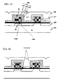
- FIG. 3A illustrates an example of operation voltages at erasing.
- the voltages shown are a case where the semiconductor substrate 101 is a p-type of the semiconductor substrate. If the semiconductor substrate 101 of an n-type is employed, the region 109 is n+, and the positive and negative in the operation voltages are inverted.
- An inversion layer 1000 is formed below the assist gate 107 and immediately below the gate insulating film 106. The inversion layer 1000 is extremely thin, yet is shown as thin as possible in the drawing.
- a depletion region 1002 shown by a dotted line extends from the inversion layer 1000.
- FIG. 3B shows charges stored in the storage film 103. The tunneling effects between bands readily occur in a thinnest portion of the depletion layer 1002.
- a tunneling current between bands is shown as an arrow. Holes are accelerated to flow in the direction of the arrow, and become hot holes to go over the potential barrier of the tunnel oxide film 102. The hot holes are pulled by the bias applied to the word line 108 and injected into the storage film 103. Erasing is performed by neutralizing the stored electrons. Reading and writing operations are same as those described in Patent Document 1, and the description is omitted here.
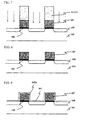
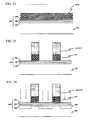
- the p-type semiconductor substrate 101 is prepared.
- the gate insulating film 106 in the assist gate 107 is formed by thermal oxidization.
- an electrode material 107a of the assist gate 107 is formed on the gate insulating film 106.
- phosphor-doped amorphous silicon is deposited by thermal CVD.
- the electrode material 107a is patterned by the lithography and etching to form the assist gate 107.
- the resist that was used in this process is remained.
- the high-concentration impurity region 109 is formed in the semiconductor substrate 101.
- An example of this process is implemented according to the following conditions. Ion-implantation (dopant: B (Boron), preferably, BF2, doze amount: 1e12- 1e17 (atoms/cm2), preferably, 1e13 - 1e16, more preferably, 1e13 - 3e14, acceleration energy: 10keV - 200keV, preferably, 10keV - 100keV, more preferably, 10keV - 70keV.
- the resist is removed in the ashing and cleaning process by using solution of sulfuric acid and hydrogen peroxide.
- a shown in FIG. 9 the tunnel oxide film 102 is formed.
- the periphery of the assist gate 107 is also oxidized to form an oxidized layer 102b.
- a nitride film Si 3 N 4
- the top oxide film 104 is formed by forming the oxide film by the thermal CVD.
- the word line 108 is laminated on the top oxide film 104. This process is performed by depositing undoped polysilicon by the thermal CVD, an impurity such as As or P is injected into polysilicon, and then the polysilicon is etched in the lateral direction by the lithography and etching processes.
- the ONO structure in which the tunnel oxide film, the storage nitride film, and the top oxide film are sequentially laminated.
- This ONO structure is formed after the assist gate is formed, and there is not provided a sidewall on a side wall of the assist gate.
- the surface region of the semiconductor substrate is cut out in U shape between the assist gates.
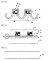
- FIG. 13 is a cross-sectional view illustrating the memory cell of a second embodiment.
- the same components and configurations as those of FIG. 2 have the same reference numerals.
- both the tunnel film 102 and the top film 104 are configured to be the oxide films having the thicknesses equal to or greater than 4 nm, which is equal to the thickness for the FN tunneling region.
- the U-shaped cutout between the assist gates adjacently arranged to each other in the surface region of the semiconductor substrate there is provided the U-shaped cutout between the assist gates adjacently arranged to each other in the surface region of the semiconductor substrate.
- the aforementioned U-shaped cutout namely a substantially U-shaped recess can be processed by the known photolithography technique and dry etching technique, as will be described later.
- This u-shaped recess provided on the surface of the semiconductor substrate 101 makes the channel longer than that of the first embodiment. Therefore, even if the resistance to the short-channel effects becomes high and the memory cell array is to be downsized, there are characteristics the operation margin is allowed as a device.
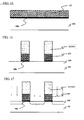
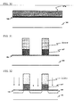
- the p-type semiconductor substrate 101 is prepared. Then, as shown in FIG. 15, the gate insulating film 106 in the assist gate 107 is formed by the thermal oxidization. Then, the electrode material 107a of the assist gate 107 is formed on the gate insulating film 106. For example, phosphor (P)-doped amorphous silicon is deposited by the thermal CVD. Then, as shown in FIG. 16, the electrode material 107a is patterned by the lithography and etching to form the assist gate 107. The resist that was used in this process is remained. Next, as shown in FIG. 17, the high-concentration impurity region 109 is formed in the semiconductor substrate 101. An example of this process is implemented according to the following conditions.
- Ion-implantation preferably, BF2
- doze amount 1e12 - 1e17 (atoms/cm2), preferably, 1e13 - 1e16, more preferably, 1e13 - 3e14
- acceleration energy 10keV - 200keV, preferably, 10keV - 100keV, more preferably, 10keV-70keV.
- a U-shaped recess 121 is formed in the semiconductor substrate 101.
- the resist is removed in the ashing and cleaning process by using solution of sulfuric acid and hydrogen peroxide.
- the tunnel oxide film 102 is laminated on the whole surface of the semiconductor substrate 101 by the thermal oxidization or plasma oxidization.
- the tunnel oxide film 102 has to be formed inside the U-shaped recess 121, and accordingly, it is desirable that the tunnel oxide film 102 should be formed uniformly in a method that is less dependent on the plane orientation in the substrate crystal. It is desirable that the thermal oxidization should be employed for the plane substrate in view of the quality of the film.
- the plasma oxidization is known as an oxidizing method that is in no way inferior to the thermal oxidization in view of the quality of the film and that has little dependency on the plane orientation.
- the plasma oxidization denotes that a gas including an oxygen gas is formed into plasma with the use of microwaves or RF, and the wafer surface is exposed to the plasma to be oxidized directly.
- a noble gas may be added to enhance the plasma density.
- He, Ne, or Ar is often used as the noble gas, and in addition, it is more desirable that Kr or Xe should lower the temperature of electrons.
- the surface wave plasma excited by the microwaves is preferable, because low irradiation energy can be realized in high density equal to or more than 1e12/cm3 and low ion irradiation energy equal to or lower than 7e.
- a radial line slot antenna should be employed in view of the evenness on the wafer surface.
- the nitride film is deposited 10 nm by the thermal CVD to form the storage film 103.
- the ONO structure in which the tunnel oxide film, the storage nitride film, and the top oxide film are sequentially laminated. This ONO structure is formed before the assist gate is formed, and there is not provided a sidewall on a side wall of the assist gate.
- FIG. 22 is a cross-sectional view illustrating the memory cell of a third embodiment.
- the assist gate 107 is formed on the ONO structure 105, which is formed on the surface of the semiconductor substrate 101.
- a reference numeral 111 shown in this figure is an insulating film formed on the top and side walls of the assist gate 107.
- the tunnel oxide film 102 included in the ONO structure 105 also serves as a gate insulating film of the assist gate 107.
- both the tunnel film 102 and the top film 104 are configured to be the oxide films having the thicknesses equal to or greater than 4 nm for the FN tunneling region.
- the tunnel film 102 in the ONO structure 105 also serves as the gate insulating film of the assist gate 107, leading to the characteristics of simplification in the fabrication process.
- the charge can be stored below the assist gate 107 and the window of the threshold value becomes wide, leading to the device operation having a margin.
- the p-type semiconductor substrate 101 is prepared.
- an ONO film 102 - 104 is formed.
- the tunnel oxidization film 102 is formed by the thermal oxidization, and then the nitride film is deposited 10 nm by the thermal CVD to form the storage film 103.
- the silicon oxide film (SiO 2 ) is deposited by the thermal CVD to form the top oxide film 104.
- the tunnel oxide film 102 is formed by the thermal oxidization, and then the nitride film is deposited 15 nm by the thermal CVD to form the storage film 103.
- the top oxide film 104 may be formed by the thermal oxidization (wet oxidization) or plasma oxidization. After the ONO film 102 - 104 is formed in this manner, the electrode material 107a of phosphor-doped amorphous silicon is deposited.
- the electrode material 107a is patterned with the use of the lithography and etching to form the assist gate 107.
- the high-concentration impurity region 109 is formed in the semiconductor substrate 101.
- An example of ion-implantation in this process is shown as follows.
- the insulating film 111 is formed in the periphery of the assist gate 107 by the thermal oxidization.
- the word line 108 is formed on the top oxide film 104.
- an undoped polysilicon is deposited by the thermal CVD, for example, and then the impurity such as As or P is injected into polysilicon, and polysilicon is etched in the lateral direction by the lithography and etching processes.
- the tunnel oxide film and the storage nitride film are deposited after the assist gate is formed. Also, the sidewalls are provided on the side walls of the assist gate.
- FIG. 29 is a cross-sectional view illustrating the memory cell of a fourth embodiment.
- Sidewalls 110 are provided on side walls of the assist gate 107.
- the tunnel oxide film 102 is configured to be equal to or greater than 4 nm for the FN tunneling region.
- the charge storage region of the fourth embodiment is composed of the tunnel oxide film 102 and the storage film 103.
- the sidewalls 110 are provided on side walls of the assist gate 107, and at least the storage film (nitride film) 103 in the ONO structure 105 is not provided between the sidewalls 110.
- the storage film 103 is not provided above the assist gate 107, and accordingly the charge is programmed into the center of the channel. Therefore, there are characteristics that the difficulty of erasing and the increase in CBD (Complementary Bit Disturb) can be suppressed.
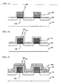
- the gate insulating film 106 is formed on the p-type semiconductor substrate 101 by the thermal oxidization, and the electrode material 107a is deposited thereon by the thermal CVD. Then, as shown in FIG. 31, the assist gate 107 is formed. Next, as shown in FIG. 32, the high-concentration impurity region 109 is formed in the semiconductor substrate 101. An example of the ion-implantation condition has been described above. Then, as shown in FIG. 33, after the resist is stripped in the ashing and cleaning processes by using solution of sulfuric acid and hydrogen peroxide, the tunnel oxide film 102 is formed.
- the gate insulating film 106 provided between the assist gates 107 is removed in the preprocessing (hydrofluoric acid), and subsequently, the semiconductor substrate 101 and the periphery of the assist gates 107 are thermally oxidized. Then, as shown in FIG. 34, the nitride film is deposited 10 nm by the thermal CVD to form the storage film 103.
- a sidewall material 110a such as SiO 2 is deposited by the thermal CVD.
- SiO 2 is etched back and stopped at the storage film 103 to form the sidewall 110.
- the nitride film between the sidewalls is removed by etching. In this case, the nitride film provided above the assist gate 107 is also removed.
- the word line 108 is formed.
- the ONO structure in which the tunnel oxide film, the storage nitride film, and the top oxide film are sequentially laminated. This ONO structure is formed before the assist gate is formed, and there are provided sidewalls on side walls of the assist gate.
- FIG. 39 is a cross-sectional view illustrating the memory cell of a fifth embodiment.
- the same components and configurations as those of FIG. 5 have the same reference numerals.
- both the tunnel oxide film 102 and the top film 104 are configured to be the oxide film equal to or greater than 4 nm for the FN tunneling region.
- the sidewalls 110 are formed on the side walls of the assist gate 107, and at least the storage film (nitride film) 103 in the ONO structure 105 is not provided between the sidewalls 110. Accordingly, the charge is programmed into the center of the channel. Therefore, there are characteristics that the difficulty in erasing and the increase in CBD (Complementary Bit Disturb) can be suppressed. In addition, there are other characteristics that the fabrication process can be simplified as in the third embodiment.
- the structure shown in FIG. 40 is formed.
- The, as shown in FIG. 41, the sidewalls 110 are formed. This process is same as those shown in FIGs. 35 and 37.
- the sidewalls 110 are made of nitride film (Si 3 N 4 ).
- the top film 104 and the storage film 103 are etched with the use of the sidewalls 110 as masks.
- the insulating film (oxide film) provided on the assist gate 107 is removed.
- the insulating film is formed again on the assist gate 107 by the thermal oxidization, for example.
- the word line 108 is formed as shown in FIG. 44.
- the semiconductor device of the present invention includes, for example, a semiconductor memory device, and a semiconductor device including the aforementioned memory as a part thereof such as system LSI.
Landscapes
- Engineering & Computer Science (AREA)
- Microelectronics & Electronic Packaging (AREA)
- Non-Volatile Memory (AREA)
- Semiconductor Memories (AREA)
Abstract
Description
- This invention generally relates to semiconductors, and more particularly, to a non-volatile memory technology of SONOS type, which enables excellent data retention characteristics and easy data erase.
- Conventionally, flash memories with the use of the floating gate technique have been widely used as non-volatile flash memories to be incorporated into the electronics devices. However, there arises limitations in that the flash memory is designed with the floating gate technique, if the memory cell is further downsized to realize high storage density in the flash memory and becomes equal to or smaller than 90 nm in the manufacturing process rule. This is because the area of the high-voltage transistor-forming region, to be provided for programming and erasing data, inevitably becomes relatively wide in a small-sized memory of the floating gate type, resulting in a rise in the manufacturing costs, or it becomes difficult to reduce a cell portion without degrading the reliability due to the possibility of memory error or data loss.
- On the other hand, the non-volatile memory having a thin film storage region stores a memory bit by storing the charge between two insulation films (oxide films) provided below the gate made of polysilicon. The non-volatile memory of the aforementioned thin film storage system includes the non-volatile memory of SONOS (Silicon Oxide Nitride Oxide Silicon) type and the nanocrystal memory, in which the charge is stored in the silicon nitride film (ONO: oxide film/nitride film/oxide film) sandwiched by the silicon oxide films. The above-mentioned thin film storage method is designed so that the trap (or nanocrystal) in the nitride film may retain the charge, and the stored charge is prevented from moving to another storage region. Accordingly, the above-mentioned thin film storage method has characteristics that the charge loss is suppressed and the data retention characteristics are improved, although the charge loss may occur in the floating gate method.
- Now, in the technical field of the non-volatile memory, there is known an NROM (nitride read-only memory) having two bits/cell, as a memory cell structure in which a unit cell is designed to include multiple-bits (for example, refer to Patent Document 1 and the cited documents therein).
- FIG. 1 is a view illustrating the operation principle of the NROM, and schematically shows a cross-sectional view of a unit cell of the NROM. This NROM includes first and
second bit lines LOCOS 13 of a thin film is arranged thereon, and an ONO structure (oxide film/nitride film/oxide film) 14 is arranged on a surface region of the semiconductor substrate provided between theLOCOS 13. A word line (gate line) of polysilicon is formed so that the gate may be formed in the surface region of asemiconductor substrate 11 provided below the ONO structure 14 (below theLOCOS 13 of the thin film region). That is to say, the NROM memory cell transistor substantially has the same fundamental structure as that of a conventional n-channel MOS-FET, yet an electron capture layer of the ONO structure is employed instead of a gate dielectric film. - In programming the cell of the above-mentioned NROM, for example, a given bias Vg is applied to the
gate line 15 and a positive bias Vb2 is applied to thesecond bit line 12b whereas thefirst bit line 12a is grounded. Then, a channel is formed between thefirst bit line 12a and thesecond bit line 12b and electrons flowing to thesecond bit line 12b from thefirst bit line 12a are captured and stored in one end region (a second bit) 16b in theONO structure 14. - Additionally, if the bias conditions that are applied to the
first bit line 12a and thesecond bit line 12b are reversed, the electrons flowing to thefirst bit line 12a from thesecond bit line 12b are captured and stored in the other end region (a first bit) 16a in theONO structure 14. - In contrast, in reading the cell of the above-mentioned NROM, a given bias Vg' is applied to the
gate line 15 and a positive bias Vbl' is applied to thebit line 12a whereas thesecond bit line 12b is grounded. Then, (the second bit) 16b can be read. Also, if the bias conditions that are applied to thefirst bit line 12a and thesecond bit line 12b are reversed, (the first bit) 16a can be read. - In addition, the width of the
first bit 16a and that of thesecond bit 16b of the electron capture regions are designed to be sufficiently thinner than that of the channel formed between the twobit lines bits Japanese Patent Application Publication 2001-156275 - As described above, two pieces of bit information can be stored in the NROM by reversing the bias conditions to be applied to the
first bit line 12a and thesecond bit line 12b. Assuming that the minimum process size is set to F, the miniaturization of 4F2 can be attained in each cell, enabling a highly integrated memory. - Now, the minimum process size F is determined by the minimum process line width of the photolithography, and there are following difficulties in order to realize the cell having the area of 4F2.
- When a virtual ground array structure is produced, the buried line is generally formed by the diffusion layer to be used for the source line or bit line according to the purpose in each case. However, the afore-mentioned diffusion layer is formed by ion-implantation. The implanted ions are bombarded onto the crystal lattice of the silicon substrate or diffused in the silicon crystal by the thermal treatment to be done after the ion-implantation. This makes it difficult to downsize the width of the diffusion layer to the limit of the photolithography technique. Moreover, if the self-align process with the use of the hard mask is employed by providing the sidewall to overcome the aforementioned limit in the photolithography technique, the device fabrication process will be complicated.
- The present invention has been made in view of the above circumstance and has the object of providing the technique for the non-volatile memory of SONOS type that enables excellent data retention characteristics and easy data deletion.
- According to an aspect of the present invention, preferably, there is provided a semiconductor device including a semiconductor substrate of a chosen conductivity type, a charge storage region including a tunnel oxide film and a storage film provided below a word line and provided above the semiconductor substrate, assist gates provided on a gate insulating film on the semiconductor substrate, and a high-concentration impurity region that is provided in the semiconductor substrate and is located between adjacent assist gates, the high-concentration impurity region having the same conductivity type as that of the semiconductor substrate.
- On the above-mentioned semiconductor device, the high-concentration impurity region may extend up to outer edges of the adjacent assist gates. The tunnel oxide film may have a thickness equal to or greater than any of 4 nm, 5 nm, 6 nm, 7 nm, and 10 nm. The charge storage region may include a top oxide film provided on the storage film, and at least one of the tunnel oxide film and the top oxide film has a thickness equal to or greater than any of 4 nm, nm, 6 nm, 7 nm, and 10 nm. Preferably, the tunnel oxide film may have a thickness in which FN tunneling is dominant. The above-mentioned semiconductor device may further include sidewalls provided along sides of the assist gates. Preferably, the sidewalls are parts of the charge storage region provided along the sides of the assist gates. The charge storage region may be located below the assist gates. The tunnel oxide film may include a gate insulating film provided below the assist gates. The charge storage region may be provided so as to cover the assist gates. The above-mentioned semiconductor device may further include a substantially U-shaped recess provided in the semiconductor substrate and located between adjacent assist gates.
- According to another aspect of the present invention, preferably, there is provided a method of fabricating a semiconductor device comprising the steps of forming assist gates on a gate insulating film on a semiconductor substrate of a chosen conductivity type, forming a high-concentration impurity region in the semiconductor substrate and located between adjacent assist gates, the high-concentration impurity region having the same conductivity type as that of the semiconductor substrate, and forming a charge storage region above the semiconductor substrate and composed of at least a tunnel oxide film and a storage film. The above-mentioned semiconductor device may further include a step of forming a substantially U-shaped recess provided in the semiconductor substrate and located between adjacent assist gates. The above-mentioned semiconductor device may further include a step of forming sidewalls along sides of the assist gates.
- According to another aspect of the present invention, preferably, there is provided a semiconductor device including a semiconductor substrate, a charge storage region including a tunnel oxide film and a storage film provided below a word line and provided above the semiconductor substrate, assist gates provided on a gate insulating film on the semiconductor substrate, and a substantially U-shaped recess in the semiconductor substrate and located between adjacent assist gates.
- According to the present invention, firstly, both the thickness of a tunnel film and that of a top film provided thereon are configured to be an FN tunneling region (4 nm or more). It is therefore possible to provide a non-volatile memory technique of SONOS type having high data retention characteristics.
- According to the present invention, secondly, a high-concentration impurity region of a conductivity type same as that of the substrate is provided in a substrate region arranged between assist gates adjacently provided to each other. This makes it possible to provide the non-volatile memory technique of SONOS type that realizes easy data erase.
-
- [FIG. 1] FIG. 1 schematically shows a cross-sectional view of a unit cell of a NROM to illustrate the operation principle thereof;
- [FIG. 2] FIG. 2 is a cross-sectional view of a memory cell in accordance with a first embodiment of the present invention;
- [FIG. 3] FIG. 3 is a view showing the principle of operation of the first embodiment;
- [FIG. 4] FIG. 4 is a view showing a (first) fabrication method of the first embodiment;
- [FIG. 5] FIG. 5 is a view showing a (second) fabrication method of the first embodiment;
- [FIG. 6] FIG. 6 is a view showing a (third) fabrication method of the first embodiment;
- [FIG. 7] FIG. 7 is a view showing a (fourth) fabrication method of the first embodiment;
- [FIG. 8] FIG. 8 is a view showing a (fifth) fabrication method of the first embodiment;
- [FIG. 9] FIG. 9 is a view showing a (sixth) fabrication method of the first embodiment;
- [FIG. 10] FIG. 10 is a view showing a (seventh) fabrication method of the first embodiment;
- [FIG. 11] FIG. 11 is a view showing a (eighth) fabrication method of the first embodiment;
- [FIG. 12] FIG. 12 is a view showing a (ninth) fabrication method of the first embodiment;
- [FIG. 13] FIG. 13 is a cross-sectional view of a memory cell in accordance with a second embodiment of the present invention;
- [FIG. 14] FIG. 14 is a view showing a (first) fabrication method of the second embodiment;
- [FIG. 15] FIG. 15 is a view showing a (second) fabrication method of the second embodiment;
- [FIG. 16] FIG. 16 is a view showing a (third) fabrication method of the second embodiment;
- [FIG. 17] FIG. 17 is a view showing a (fourth) fabrication method of the second embodiment;
- [FIG. 18] FIG. 18 is a view showing a (fifth) fabrication method of the second embodiment;
- [FIG. 19] FIG. 19 is a view showing a (sixth) fabrication method of the second embodiment;
- [FIG. 20] FIG. 20 is a view showing a (seventh) fabrication method of the second embodiment;
- [FIG. 21] FIG. 21 is a view showing a (eighth) fabrication method of the second embodiment;
- [FIG. 22] FIG. 22 is a cross-sectional view of a memory cell in accordance with a third embodiment of the present invention;
- [FIG. 23] FIG. 23 is a view showing a (first) fabrication method of the third embodiment;
- [FIG. 24] FIG. 24 is a view showing a (second) fabrication method of the third embodiment;
- [FIG. 25] FIG. 25 is a view showing a (third) fabrication method of the third embodiment;
- [FIG. 26] FIG. 26 is a view showing a (fourth) fabrication method of the third embodiment;
- [FIG. 27] FIG. 27 is a view showing a (fifth) fabrication method of the third embodiment;
- [FIG. 28] FIG. 28 is a view showing a (sixth) fabrication method of the third embodiment;
- [FIG. 29] FIG. 29 is a view showing the principle of operation of the fourth embodiment;
- [FIG. 30] FIG. 30 is a view showing a (first) fabrication method of the fourth embodiment;
- [FIG. 31] FIG. 31 is a view showing a (second) fabrication method of the fourth embodiment;
- [FIG. 32] FIG. 32 is a view showing a (third) fabrication method of the fourth embodiment;
- [FIG. 33] FIG. 33 is a view showing a (fourth) fabrication method of the fourth embodiment;
- [FIG. 34] FIG. 34 is a view showing a (fifth) fabrication method of the fourth embodiment;
- [FIG. 35] FIG. 35 is a view showing a (sixth) fabrication method of the fourth embodiment;
- [FIG. 36] FIG. 36 is a view showing a (seventh) fabrication method of the fourth embodiment;
- [FIG. 37] FIG. 37 is a view showing a (eighth) fabrication method of the fourth embodiment;
- [FIG. 38] FIG. 38 is a view showing a (ninth) fabrication method of the fourth embodiment;
- [FIG. 39] FIG. 39 is a cross-sectional view of a memory cell in accordance with a fifth embodiment of the present invention;
- [FIG. 40] FIG. 40 is a view showing a (first) fabrication method of the fifth embodiment;
- [FIG. 41] FIG. 41 is a view showing a (second) fabrication method of the fifth embodiment;
- [FIG. 42] FIG. 42 is a view showing a (third) fabrication method of the fifth embodiment;
- [FIG. 43] FIG. 43 is a view showing a (fourth) fabrication method of the fifth embodiment; and
- [FIG. 44] FIG. 44 is a view showing a (fifth) fabrication method of the fifth embodiment.
- A description will now be given, with reference to the accompanying drawings, of embodiments of the present invention.
- On a semiconductor memory device of the present invention, as will be described later in more detail, firstly, the storage film is sandwiched from top and bottom to form the ONO structure (a charge storage region) including a tunnel film and a top film. Both the thickness of the tunnel film and that of the top film are configured to be the FN tunneling region (4 nm or more). The data retention characteristics can be enhanced by configuring both the thickness of the tunnel film and that of the top film to be the FN tunneling region.
- Secondly, assist gates are provided, and a high-concentration impurity region of a conductivity type same as that of the substrate is located between assist gates adjacently arranged to each other, in a region close to the surface of the substrate. The aforementioned high-concentration impurity region extends up to lower regions of outer edges of the assist gates. By providing the high-concentration impurity region as described, a depletion layer, to be formed between an inversion layer and the high-concentration impurity region adjacently provided thereto, is made thin drastically, when the bias is applied to the assist gates. For this reason, the depletion layer can be made thin in an end region of the inversion layer (namely, the lower regions of outer edges of the assist gates), whereas the depletion region is conventionally arranged uniformly in the periphery of the inversion region according to the conventional structure. Therefore, a high electric field is applied to the depletion region and hot holes are generated between bands. The hot holes are injected into the charge storage region in the storage film of the ONO structure and pairs of electron and electron hole stored in this region disappear, leading to easy data erase.
- A description will be given of theoretical consideration that has lead to the present invention, before embodiments of the present invention are described. The diffusion layer is formed by ion-implantation to be used for the buried line (source line or bit line), yet it is difficult to downsize the width of the diffusion layer to the limit of the photolithography, because the implanted ions are bombarded with the crystal lattice or diffused due to the subsequent thermal treatment, as described above. The assist gate is provided on the electrode side to solve the above-mentioned drawback. The inversion layer, which is formed by applying the bias to the assist gate, is used as a wiring layer. This does not have to change the process size of the assist gate and the inversion layer can be used as the "buried line", enabling to downsize the width of the diffusion layer to the limit of photolithography.
- There is another structure example of memory cell "the third embodiment of the memory cell" of Patent Document 1 (hereinafter referred to as related art), which has been proposed on the basis of the conception similar to the above-mentioned consideration. However, this related art has the problem in the configuration of the thickness of the oxide film in view of the data retention, as will be described hereafter.
- On this related art, the MOS inversion layer in the switch transistor is used as the wiring instead of the wiring of the diffusion layer in the memory cell. The hot electron is injected into the source side at the time of writing, and the current of the same direction is detected at the time of reading. This makes it possible to operate in the opposite direction in the memory cell, enabling two-bit operation in one memory cell. The tunnel oxide film formed in the memory transistor is configured to have the thickness of 5 nm (for the FN tunneling region), and the top oxide film provided thereabove is configured to have the thickness of 3 nm (in the direct tunneling region). The electron is extracted to the gate electrode side for erasing.
- Paten document 1 does not explicitly describe, yet the following reasons can be considered why the above-mentioned configuration has been employed. On the related art, the memory cell array is configured without the diffusion layer. If the electron is tried to be extracted to the substrate side, it is necessary to extract the electron to the inversion layer. However, under the bias condition convenient to extract the electron (namely, negative gate electrode), the inversion layer does not extend from the lower portion of the assist gate. That is to say, the inversion layer does not reach the region in which the charge is stored (namely, the channel region). Hence, the electron cannot be extracted to the substrate side. On this account, the electron inevitably has to be extracted to the gate electrode side.
- The top oxide film is needed to be thin approximately 3 nm to extract the electron may in this manner, because of the following reasons. As is well known, the electron conduction mechanism in the oxide film having the thickness of approximately at most 10 nm is categorized into the FN tunneling and direct tunneling. The actual electron conduction can be regarded as the sum of the aforementioned two conduction mechanisms.
- In the two mechanisms, the FN tunneling effect is dominant, when the oxide film has the thickness of at least 4 nm, and is dominant when the thickness is 5 nm, in particular. The current size of the FN tunneling is dependent on the size of the electric field, and is not dependent on the thickness of the oxide film. In contrast, the direct tunneling effect is dominant when the thickness is less than 4 nm, and is dominant when the thickness is 3 nm or less, in particular. The current amount varies depending on the thickness of the oxide film, even if the strengths of the electric fields are the same.
- The data to be erased by extracting the electron has choices whether the electron is extracted to the gate electrode side or to the substrate side. It is necessary to make the oxide film to which the electron is extracted thin enough to be equal to the thickness of the direct tunneling region, to whichever the electron is extracted. This is because the conduction mechanism of the FN tunneling is dependent only on the strength of the electric field applied. Even if there is a difference in the thickness of the oxide film in the thickness range for the FN tunneling region (the thickness range of 4 nm or more), the electrons are flown from the opposite side at the same time as the electrons are extracted. This makes it difficult to erase substantially. On the above-mentioned related art, erasing is performed by extracting the electron to the gate electrode side. The top oxide film is designed to have the thickness of 3 nm, same as that of the direct tunneling region, which is thinner than that of the tunnel film (the FN tunneling region) of 5 nm.
- However, if any of the top film and the tunnel film has the thickness equal to that of the oxide film in the direct tunneling region, there is the problem in that the data retention characteristics are inferior to a case where both the top film and the tunnel film employ the oxide film having the thickness for the FN tunneling region.
- Therefore, according to the present invention, the thickness of the tunnel film and that of the top film are configured to be the FN tunneling region. Specifically, these thicknesses are configured to be equal to or greater than 4 nm. The data retention characteristics can be enhanced by configuring both the tunnel film and the top film to have the thicknesses for the FN tunneling region. It is preferable that these thicknesses should be configured to be equal to or greater than 4 nm, for example, equal to or greater than 5 nm. Preferably, they should be equal to or greater than 7 nm. More preferably, they should be equal to or greater than 10 nm. As the thickness of the film increases, the data retention characteristics can be improved.
- In addition, erasing is difficult by only employing the thickness for the FN tunneling region for the thickness of the tunnel film and that of the top film. Further, if the tunnel film and the top film have the same thickness and even if the thickness is equal to that of the direct tunneling region, there will arise the problem in that erasing is difficult in the same way that the both the tunnel film and the top film have the thicknesses for the FN tunneling region, because the dependency on the electric field is equal in the conductivity of the both films.
- Accordingly, a high-concentration impurity region having the same conductivity type as that of the substrate is provided on the substrate region between the assist gates adjacently provided in accordance with the present invention. If the aforementioned high-concentration impurity region is provided, the depletion layer, to be formed between the inversion layer and the high-concentration impurity region adjacently arranged thereto, extremely becomes thin at the time of applying the bias to the assist gates. This applies a high electric field to the depletion layer and the hot holes are generated between the bands. These hot holes are injected into the charge storage region having the ONO structure and form pairs with the electrons stored in this region, enabling easy data erasing. Here, as a bias at the time of erasing, for example, 0 V is applied to the substrate, 5 V is applied to the inversion layer, 8 V is applied to the assist gate, and -5 V is applied to the word line.
- A description will be given of embodiments of the present invention.
- In the present embodiment, there is provided an ONO structure in which a tunnel oxide film, a storage nitride film, and a top oxide film are sequentially laminated. This ONO structure is formed after the assist gate is formed, and there is not provided a sidewall on a side wall of the assist gate.
- FIG. 2 is a view illustrating a cross-sectional view of the memory cell in accordance with a first embodiment of the present invention. In this figure, a
reference numeral 101 represents a semiconductor substrate, areference numeral 102 represents a tunnel oxide film, areference numeral 103 represents a storage film of silicon nitride film, and areference numeral 104 represents a top oxide film provided on thestorage film 103. A laminated structure of thetunnel oxide film 102, thestorage film 103, and thetop oxide film 104 forms anONO structure 105. As described above, both thetunnel film 102 and thetop film 104 are configured to be the oxide films having the thicknesses at least 4 nm for the FN tunneling region. - The
ONO structure 105 is formed to cover anassist gate 107 and agate insulating film 106, which is formed at given intervals on the surface of thesemiconductor substrate 101. The assistgates 107 are arranged on thegate insulating films 106 at given intervals. Aword line 108 is laminated on the whole surface of theONO structure 105. A high-concentration impurity region 109 is provided between theassist gates 107 in a surface region of thesemiconductor substrate 101. Theimpurity region 109 has a conductivity type same as that of thesemiconductor substrate 101. Thesemiconductor substrate 101 is a p-type silicon substrate, and accordingly, the high-concentration impurity region 109 is p+. - The aforementioned configuration, as compared to that of the related art, there are different points in that the high-
concentration impurity region 109 is provided between theassist gates 107 in the surface region of thesemiconductor substrate 101 and both thetunnel film 102 and thetop film 104 have the thicknesses equal to or greater than 4 nm. - In the first embodiment, the data retention characteristics can be enhanced because of the above-described reasons and the data can be erased easily. In addition, the
gate insulating film 106 provided below theassist gate 107 can be made thinner than theONO structure 105. There are characteristics that the inversion layer serving as the wiring allows the operation margin. - FIG. 3A illustrates an example of operation voltages at erasing. The voltages shown are a case where the
semiconductor substrate 101 is a p-type of the semiconductor substrate. If thesemiconductor substrate 101 of an n-type is employed, theregion 109 is n+, and the positive and negative in the operation voltages are inverted. Aninversion layer 1000 is formed below theassist gate 107 and immediately below thegate insulating film 106. Theinversion layer 1000 is extremely thin, yet is shown as thin as possible in the drawing. Adepletion region 1002 shown by a dotted line extends from theinversion layer 1000. FIG. 3B shows charges stored in thestorage film 103. The tunneling effects between bands readily occur in a thinnest portion of thedepletion layer 1002. A tunneling current between bands is shown as an arrow. Holes are accelerated to flow in the direction of the arrow, and become hot holes to go over the potential barrier of thetunnel oxide film 102. The hot holes are pulled by the bias applied to theword line 108 and injected into thestorage film 103. Erasing is performed by neutralizing the stored electrons. Reading and writing operations are same as those described in Patent Document 1, and the description is omitted here. - Next, a description will be given of a fabrication method of the first embodiment. As shown in FIG. 4, for example, the p-
type semiconductor substrate 101 is prepared. Then, as shown in FIG. 5, thegate insulating film 106 in theassist gate 107 is formed by thermal oxidization. Then, anelectrode material 107a of theassist gate 107 is formed on thegate insulating film 106. For example, phosphor-doped amorphous silicon is deposited by thermal CVD. Then, as shown in FIG. 6, theelectrode material 107a is patterned by the lithography and etching to form theassist gate 107. The resist that was used in this process is remained. Next, as shown in FIG. 7, the high-concentration impurity region 109 is formed in thesemiconductor substrate 101. An example of this process is implemented according to the following conditions. Ion-implantation (dopant: B (Boron), preferably, BF2, doze amount: 1e12- 1e17 (atoms/cm2), preferably, 1e13 - 1e16, more preferably, 1e13 - 3e14, acceleration energy: 10keV - 200keV, preferably, 10keV - 100keV, more preferably, 10keV - 70keV. - Next, as shown in FIG. 8, the resist is removed in the ashing and cleaning process by using solution of sulfuric acid and hydrogen peroxide. Then, a shown in FIG. 9, the
tunnel oxide film 102 is formed. In this case, the periphery of theassist gate 107 is also oxidized to form an oxidizedlayer 102b. Next, as shown in FIG 10, a nitride film (Si3N4) is deposited by the thermal CVD to form thestorage film 103. Then, as shown in FIG. 11, thetop oxide film 104 is formed by forming the oxide film by the thermal CVD. Lastly, as shown in FIG 12 theword line 108 is laminated on thetop oxide film 104. This process is performed by depositing undoped polysilicon by the thermal CVD, an impurity such as As or P is injected into polysilicon, and then the polysilicon is etched in the lateral direction by the lithography and etching processes. - In the present embodiment, there is provided the ONO structure in which the tunnel oxide film, the storage nitride film, and the top oxide film are sequentially laminated. This ONO structure is formed after the assist gate is formed, and there is not provided a sidewall on a side wall of the assist gate. In addition, the surface region of the semiconductor substrate is cut out in U shape between the assist gates.
- FIG. 13 is a cross-sectional view illustrating the memory cell of a second embodiment. In this figure, the same components and configurations as those of FIG. 2 have the same reference numerals. Also in the second embodiment, both the
tunnel film 102 and thetop film 104 are configured to be the oxide films having the thicknesses equal to or greater than 4 nm, which is equal to the thickness for the FN tunneling region. - In the second embodiment, there is provided the U-shaped cutout between the assist gates adjacently arranged to each other in the surface region of the semiconductor substrate. The aforementioned U-shaped cutout, namely a substantially U-shaped recess can be processed by the known photolithography technique and dry etching technique, as will be described later.
- This u-shaped recess provided on the surface of the
semiconductor substrate 101 makes the channel longer than that of the first embodiment. Therefore, even if the resistance to the short-channel effects becomes high and the memory cell array is to be downsized, there are characteristics the operation margin is allowed as a device. - As shown in fig. 14, the p-
type semiconductor substrate 101 is prepared. Then, as shown in FIG. 15, thegate insulating film 106 in theassist gate 107 is formed by the thermal oxidization. Then, theelectrode material 107a of theassist gate 107 is formed on thegate insulating film 106. For example, phosphor (P)-doped amorphous silicon is deposited by the thermal CVD. Then, as shown in FIG. 16, theelectrode material 107a is patterned by the lithography and etching to form theassist gate 107. The resist that was used in this process is remained. Next, as shown in FIG. 17, the high-concentration impurity region 109 is formed in thesemiconductor substrate 101. An example of this process is implemented according to the following conditions. Ion-implantation (dopant: B (Boron), preferably, BF2, doze amount: 1e12 - 1e17 (atoms/cm2), preferably, 1e13 - 1e16, more preferably, 1e13 - 3e14, acceleration energy: 10keV - 200keV, preferably, 10keV - 100keV, more preferably, 10keV-70keV. - Next, as shown in FIG. 18, a U-shaped recess 121 is formed in the
semiconductor substrate 101. Then, as shown in FIG. 19, the resist is removed in the ashing and cleaning process by using solution of sulfuric acid and hydrogen peroxide. Then, as shown in FIG. 20, thetunnel oxide film 102 is laminated on the whole surface of thesemiconductor substrate 101 by the thermal oxidization or plasma oxidization. Thetunnel oxide film 102 has to be formed inside the U-shaped recess 121, and accordingly, it is desirable that thetunnel oxide film 102 should be formed uniformly in a method that is less dependent on the plane orientation in the substrate crystal. It is desirable that the thermal oxidization should be employed for the plane substrate in view of the quality of the film. However, the dependency on the plane orientation is large inside the recess having the above-mentioned curvature, resulting in a problem of uneven film thickness. Therefore, it is desirable that plasma oxidization should be used. The plasma oxidization is known as an oxidizing method that is in no way inferior to the thermal oxidization in view of the quality of the film and that has little dependency on the plane orientation. The plasma oxidization denotes that a gas including an oxygen gas is formed into plasma with the use of microwaves or RF, and the wafer surface is exposed to the plasma to be oxidized directly. In particular, a noble gas may be added to enhance the plasma density. He, Ne, or Ar is often used as the noble gas, and in addition, it is more desirable that Kr or Xe should lower the temperature of electrons. Further, the surface wave plasma excited by the microwaves is preferable, because low irradiation energy can be realized in high density equal to or more than 1e12/cm3 and low ion irradiation energy equal to or lower than 7e. Moreover, it is further preferable that a radial line slot antenna should be employed in view of the evenness on the wafer surface. - Then, as shown in FIG. 21, the nitride film is deposited 10 nm by the thermal CVD to form the
storage film 103. - In the present embodiment, there is provided the ONO structure in which the tunnel oxide film, the storage nitride film, and the top oxide film are sequentially laminated. This ONO structure is formed before the assist gate is formed, and there is not provided a sidewall on a side wall of the assist gate.
- FIG. 22 is a cross-sectional view illustrating the memory cell of a third embodiment. In this figure, the same components and configurations as those of FIG. 2 have the same reference numerals. The
assist gate 107 is formed on theONO structure 105, which is formed on the surface of thesemiconductor substrate 101. Areference numeral 111 shown in this figure is an insulating film formed on the top and side walls of theassist gate 107. - In this configuration, the
tunnel oxide film 102 included in theONO structure 105 also serves as a gate insulating film of theassist gate 107. Here, both thetunnel film 102 and thetop film 104 are configured to be the oxide films having the thicknesses equal to or greater than 4 nm for the FN tunneling region. - In the third embodiment, the
tunnel film 102 in theONO structure 105 also serves as the gate insulating film of theassist gate 107, leading to the characteristics of simplification in the fabrication process. In addition, the charge can be stored below theassist gate 107 and the window of the threshold value becomes wide, leading to the device operation having a margin. - Next, a description will be given of the fabrication process in accordance with the third embodiment. As shown in FIG. 23, firstly, the p-
type semiconductor substrate 101 is prepared. Then as shown in FIG. 24, an ONO film 102 - 104 is formed. For example, thetunnel oxidization film 102 is formed by the thermal oxidization, and then the nitride film is deposited 10 nm by the thermal CVD to form thestorage film 103. Lastly, the silicon oxide film (SiO2) is deposited by the thermal CVD to form thetop oxide film 104. Instead of the aforementioned method, thetunnel oxide film 102 is formed by the thermal oxidization, and then the nitride film is deposited 15 nm by the thermal CVD to form thestorage film 103. Lastly, thetop oxide film 104 may be formed by the thermal oxidization (wet oxidization) or plasma oxidization. After the ONO film 102 - 104 is formed in this manner, theelectrode material 107a of phosphor-doped amorphous silicon is deposited. - Then, as shown in FIG. 25, the
electrode material 107a is patterned with the use of the lithography and etching to form theassist gate 107. Next, as shown in FIG. 26, the high-concentration impurity region 109 is formed in thesemiconductor substrate 101. An example of ion-implantation in this process is shown as follows. Dopant: B (Boron), preferably, BF2, doze amount: 1e12 - 1e17 (atoms/cm2), preferably, 1e13 - 1e16, more preferably, 1e13 - 3e14, acceleration energy: 10keV-200keV, preferably, 10keV - 100keV, more preferably, 10keV - 70keV. Next, as shown in FIG. 27, the insulatingfilm 111 is formed in the periphery of theassist gate 107 by the thermal oxidization. Lastly, theword line 108 is formed on thetop oxide film 104. In this process, an undoped polysilicon is deposited by the thermal CVD, for example, and then the impurity such as As or P is injected into polysilicon, and polysilicon is etched in the lateral direction by the lithography and etching processes. FOURTH EMBODIMENT - In the present embodiment, the tunnel oxide film and the storage nitride film are deposited after the assist gate is formed. Also, the sidewalls are provided on the side walls of the assist gate.
- FIG. 29 is a cross-sectional view illustrating the memory cell of a fourth embodiment. In this figure, the same components and configurations as those of FIG. 2 have the same reference numerals.
Sidewalls 110 are provided on side walls of theassist gate 107. Here, as described, thetunnel oxide film 102 is configured to be equal to or greater than 4 nm for the FN tunneling region. The charge storage region of the fourth embodiment is composed of thetunnel oxide film 102 and thestorage film 103. - In the present embodiment, the
sidewalls 110 are provided on side walls of theassist gate 107, and at least the storage film (nitride film) 103 in theONO structure 105 is not provided between thesidewalls 110. - In the fourth embodiment, the
storage film 103 is not provided above theassist gate 107, and accordingly the charge is programmed into the center of the channel. Therefore, there are characteristics that the difficulty of erasing and the increase in CBD (Complementary Bit Disturb) can be suppressed. - Next, a description will be given of the fabrication method of the fourth embodiment. First, as shown in FIG. 30, the
gate insulating film 106 is formed on the p-type semiconductor substrate 101 by the thermal oxidization, and theelectrode material 107a is deposited thereon by the thermal CVD. Then, as shown in FIG. 31, theassist gate 107 is formed. Next, as shown in FIG. 32, the high-concentration impurity region 109 is formed in thesemiconductor substrate 101. An example of the ion-implantation condition has been described above. Then, as shown in FIG. 33, after the resist is stripped in the ashing and cleaning processes by using solution of sulfuric acid and hydrogen peroxide, thetunnel oxide film 102 is formed. In this case, thegate insulating film 106 provided between theassist gates 107 is removed in the preprocessing (hydrofluoric acid), and subsequently, thesemiconductor substrate 101 and the periphery of theassist gates 107 are thermally oxidized. Then, as shown in FIG. 34, the nitride film is deposited 10 nm by the thermal CVD to form thestorage film 103. - Next, as shown in FIG. 35, a
sidewall material 110a such as SiO2 is deposited by the thermal CVD. As shown in FIG. 36, SiO2 is etched back and stopped at thestorage film 103 to form thesidewall 110. Then, as shown in FIG. 37, the nitride film between the sidewalls is removed by etching. In this case, the nitride film provided above theassist gate 107 is also removed. Lastly, as shown in FIG. 38, theword line 108 is formed. - In the present embodiment, there is provided the ONO structure in which the tunnel oxide film, the storage nitride film, and the top oxide film are sequentially laminated. This ONO structure is formed before the assist gate is formed, and there are provided sidewalls on side walls of the assist gate.
- FIG. 39 is a cross-sectional view illustrating the memory cell of a fifth embodiment. In this figure, the same components and configurations as those of FIG. 5 have the same reference numerals. Here, as described, both the
tunnel oxide film 102 and thetop film 104 are configured to be the oxide film equal to or greater than 4 nm for the FN tunneling region. - In this embodiment, as in the fourth embodiment, the
sidewalls 110 are formed on the side walls of theassist gate 107, and at least the storage film (nitride film) 103 in theONO structure 105 is not provided between thesidewalls 110. Accordingly, the charge is programmed into the center of the channel. Therefore, there are characteristics that the difficulty in erasing and the increase in CBD (Complementary Bit Disturb) can be suppressed. In addition, there are other characteristics that the fabrication process can be simplified as in the third embodiment. - Next, a description will be given of the fabrication method of the fifth embodiment. After passing the steps in FIGs. 23 through 27, the structure shown in FIG. 40 is formed. The, as shown in FIG. 41, the
sidewalls 110 are formed. This process is same as those shown in FIGs. 35 and 37. Thesidewalls 110 are made of nitride film (Si3N4). Then, as shown in FIG. 42, thetop film 104 and thestorage film 103 are etched with the use of thesidewalls 110 as masks. In this case, the insulating film (oxide film) provided on theassist gate 107 is removed. Next, as shown in FIG. 43, the insulating film is formed again on theassist gate 107 by the thermal oxidization, for example. Lastly, theword line 108 is formed as shown in FIG. 44. - As described, according to the present invention, it is possible to provide the memory technique of the SONOS type of non-volatile memory, which enables the high data retention characteristics and simplicity in data erasing. The semiconductor device of the present invention includes, for example, a semiconductor memory device, and a semiconductor device including the aforementioned memory as a part thereof such as system LSI.
- Although a few preferred embodiments of the present invention have been shown and described, it would be appreciated by those skilled in the art that changes may be made in these embodiments without departing from the principles and spirit of the invention, the scope of which is defined in the claims and their equivalents.
Claims (23)
- A semiconductor device comprising:a semiconductor substrate of a chosen conductivity type;a charge storage region including a tunnel oxide film and a storage film provided below a word line and provided above the semiconductor substrate;assist gates provided on a gate insulating film on the semiconductor substrate; anda high-concentration impurity region that is provided in the semiconductor substrate and is located between adjacent assist gates, the high-concentration impurity region having the same conductivity type as that of the semiconductor substrate.
- The semiconductor device as claimed in claim 1, wherein the high-concentration impurity region extends up to outer edges of the adjacent assist gates.
- The semiconductor device as claimed in claim 1 or 2, wherein the tunnel oxide film has a thickness equal to or greater than 4 nm.
- The semiconductor device as claimed in claim 1 or 2, wherein the tunnel oxide film has a thickness equal to or greater than 5 nm.
- The semiconductor device as claimed in claim 1 or 2, wherein the tunnel oxide film has a thickness equal to or greater than 6 nm.
- The semiconductor device as claimed in claim 1 or 2, wherein the tunnel oxide film has a thickness equal to or greater than 7 nm.
- The semiconductor device as claimed in claim 1 or 2, wherein the tunnel oxide film has a thickness equal to or greater than 10 nm.
- The semiconductor device as claimed in claim 1 or 2, wherein the charge storage region includes a top oxide film provided on the storage film, and at least one of the tunnel oxide film and the top oxide film has a thickness equal to or greater than 4 nm.
- The semiconductor device as claimed in claim 1 or 2, wherein the charge storage region includes a top oxide film provided on the storage film, and at least one of the tunnel oxide film and the top oxide film has a thickness equal to or greater than 5 nm.
- The semiconductor device as claimed in claim 1 or 2, wherein the charge storage region includes a top oxide film provided on the storage film, and at least one of the tunnel oxide film and the top oxide film has a thickness equal to or greater than 6 nm.
- The semiconductor device as claimed in claim 1 or 2, wherein the charge storage region includes a top oxide film provided on the storage film, and at least one of the tunnel oxide film and the top oxide film has a thickness equal to or greater than 7 nm.
- The semiconductor device as claimed in claim 1 or 2, wherein the charge storage region includes a top oxide film provided on the storage film, and at least one of the tunnel oxide film and the top oxide film has a thickness equal to or greater than 10 nm.
- The semiconductor device as claimed in claim 1 or 2, wherein the tunnel oxide film has a thickness in which FN tunneling is dominant.
- The semiconductor device as claimed in any of claims 1 to 13, further comprising sidewalls provided along sides of the assist gates.
- The semiconductor device as claimed in claim 14, wherein the sidewalls are parts of the charge storage region provided along the sides of the assist gates.
- The semiconductor device as claimed in any of claims 1 to 15, wherein the charge storage region is located below the assist gates.
- The semiconductor device as claimed in claim 1, wherein the tunnel oxide film includes a gate insulating film provided below the assist gates.
- The semiconductor device as claimed in any of claims 1 to 16, wherein the charge storage region is provided so as to cover the assist gates.
- The semiconductor device as claimed in any of claims 1 to 18, further comprising a substantially U-shaped recess provided in the semiconductor substrate and located between adjacent assist gates.
- A method of fabricating a semiconductor device comprising the steps of:forming assist gates on a gate insulating film on a semiconductor substrate of a chosen conductivity type;forming a high-concentration impurity region in the semiconductor substrate and located between adjacent assist gates, the high-concentration impurity region having the same conductivity type as that of the semiconductor substrate; andforming a charge storage region above the semiconductor substrate and composed of at least a tunnel oxide film and a storage film.
- The method as claimed in claim 20, further comprising a step of forming a substantially U-shaped recess provided in the semiconductor substrate and located between adjacent assist gates.
- The method as claimed in claim 20 or 21, further comprising a step of forming sidewalls along sides of the assist gates.
- A semiconductor device comprising:a semiconductor substrate;a charge storage region including a tunnel oxide film and a storage film provided below a word line and provided above the semiconductor substrate;assist gates provided on a gate insulating film on the semiconductor substrate; anda substantially U-shaped recess in the semiconductor substrate and located between adjacent assist gates.
Applications Claiming Priority (1)
| Application Number | Priority Date | Filing Date | Title |
|---|---|---|---|
| PCT/JP2004/019647 WO2006070475A1 (en) | 2004-12-28 | 2004-12-28 | Semiconductor device |
Publications (2)
| Publication Number | Publication Date |
|---|---|
| EP1840960A1 true EP1840960A1 (en) | 2007-10-03 |
| EP1840960A4 EP1840960A4 (en) | 2008-06-04 |
Family
ID=36614602
Family Applications (1)
| Application Number | Title | Priority Date | Filing Date |
|---|---|---|---|
| EP04808002A Withdrawn EP1840960A4 (en) | 2004-12-28 | 2004-12-28 | SEMICONDUCTOR DEVICE |
Country Status (6)
| Country | Link |
|---|---|
| US (2) | US7675107B2 (en) |
| EP (1) | EP1840960A4 (en) |
| JP (1) | JP4895823B2 (en) |
| KR (1) | KR100955720B1 (en) |
| CN (1) | CN101120443B (en) |
| WO (1) | WO2006070475A1 (en) |
Families Citing this family (6)
| Publication number | Priority date | Publication date | Assignee | Title |
|---|---|---|---|---|
| US7759726B2 (en) * | 2005-07-12 | 2010-07-20 | Macronix International Co., Ltd. | Non-volatile memory device, non-volatile memory cell thereof and method of fabricating the same |
| KR100649874B1 (en) * | 2005-12-29 | 2006-11-27 | 동부일렉트로닉스 주식회사 | Transistor manufacturing method using SOH wafer |
| US8320191B2 (en) | 2007-08-30 | 2012-11-27 | Infineon Technologies Ag | Memory cell arrangement, method for controlling a memory cell, memory array and electronic device |
| KR20090025780A (en) * | 2007-09-07 | 2009-03-11 | 주식회사 하이닉스반도체 | Manufacturing Method of Flash Memory Device |
| JP2013187294A (en) * | 2012-03-07 | 2013-09-19 | Toshiba Corp | Semiconductor memory device |
| US9437470B2 (en) * | 2013-10-08 | 2016-09-06 | Cypress Semiconductor Corporation | Self-aligned trench isolation in integrated circuits |
Family Cites Families (18)
| Publication number | Priority date | Publication date | Assignee | Title |
|---|---|---|---|---|
| JP2829012B2 (en) * | 1988-12-29 | 1998-11-25 | 工業技術院長 | Semiconductor nonvolatile memory device and method of manufacturing the same |
| JPH03177074A (en) * | 1989-12-05 | 1991-08-01 | Kawasaki Steel Corp | Manufacture of semiconductor non-volatile memory device |
| JPH0629550A (en) * | 1992-07-07 | 1994-02-04 | Citizen Watch Co Ltd | Manufacture of semiconductor nonvolatile storage |
| JP4012341B2 (en) * | 1999-07-14 | 2007-11-21 | 株式会社ルネサステクノロジ | Semiconductor integrated circuit device |
| JP4058219B2 (en) * | 1999-09-17 | 2008-03-05 | 株式会社ルネサステクノロジ | Semiconductor integrated circuit |
| JP4058232B2 (en) * | 2000-11-29 | 2008-03-05 | 株式会社ルネサステクノロジ | Semiconductor device and IC card |
| JP3941517B2 (en) * | 2001-02-07 | 2007-07-04 | ソニー株式会社 | Semiconductor device and manufacturing method thereof |
| EP1248298B1 (en) * | 2001-03-26 | 2009-02-25 | Halo Lsi Design and Device Technology Inc. | Stitch and select implementation in twin monos array |
| JP2003031693A (en) * | 2001-07-19 | 2003-01-31 | Toshiba Corp | Semiconductor memory |
| JP2003309192A (en) * | 2002-04-17 | 2003-10-31 | Fujitsu Ltd | Nonvolatile semiconductor memory and method of manufacturing the same |
| DE10226964A1 (en) * | 2002-06-17 | 2004-01-08 | Infineon Technologies Ag | Method for manufacturing an NROM memory cell arrangement |
| JP2004152924A (en) * | 2002-10-30 | 2004-05-27 | Renesas Technology Corp | Semiconductor storage element and semiconductor device |
| JP2004152977A (en) * | 2002-10-30 | 2004-05-27 | Renesas Technology Corp | Semiconductor storage device |
| JP2004179387A (en) * | 2002-11-27 | 2004-06-24 | Renesas Technology Corp | Nonvolatile semiconductor memory device and method of manufacturing the same |
| JP2004221546A (en) * | 2002-12-27 | 2004-08-05 | Sharp Corp | Semiconductor storage device and portable electronic device |
| JP2004342881A (en) * | 2003-05-16 | 2004-12-02 | Sharp Corp | Semiconductor storage device, semiconductor device, IC card, portable electronic device, and method of manufacturing semiconductor storage device |
| TW594939B (en) * | 2003-06-26 | 2004-06-21 | Nanya Technology Corp | Read-only memory cell and a production method thereof |
| US6878988B1 (en) * | 2004-06-02 | 2005-04-12 | United Microelectronics Corp. | Non-volatile memory with induced bit lines |
-
2004
- 2004-12-28 EP EP04808002A patent/EP1840960A4/en not_active Withdrawn
- 2004-12-28 WO PCT/JP2004/019647 patent/WO2006070475A1/en not_active Ceased
- 2004-12-28 JP JP2006550541A patent/JP4895823B2/en not_active Expired - Fee Related
- 2004-12-28 CN CN2004800448953A patent/CN101120443B/en not_active Expired - Fee Related
- 2004-12-28 KR KR1020077014679A patent/KR100955720B1/en not_active Expired - Fee Related
-
2005
- 2005-12-27 US US11/319,999 patent/US7675107B2/en not_active Expired - Lifetime
-
2009
- 2009-10-07 US US12/574,884 patent/US7888209B2/en not_active Expired - Lifetime
Also Published As
| Publication number | Publication date |
|---|---|
| CN101120443B (en) | 2010-04-14 |
| JP4895823B2 (en) | 2012-03-14 |
| US20060231883A1 (en) | 2006-10-19 |
| US20100022081A1 (en) | 2010-01-28 |
| US7675107B2 (en) | 2010-03-09 |
| CN101120443A (en) | 2008-02-06 |
| WO2006070475A1 (en) | 2006-07-06 |
| KR20070088746A (en) | 2007-08-29 |
| US7888209B2 (en) | 2011-02-15 |
| EP1840960A4 (en) | 2008-06-04 |
| KR100955720B1 (en) | 2010-05-03 |
| JPWO2006070475A1 (en) | 2008-08-07 |
Similar Documents
| Publication | Publication Date | Title |
|---|---|---|
| TWI328881B (en) | ||
| JP4417145B2 (en) | Nonvolatile semiconductor memory device having local SONOS structure using notch gate and method of manufacturing the same | |
| US9231115B2 (en) | Semiconductor device and manufacturing method thereof | |
| JP4104133B2 (en) | Nonvolatile semiconductor memory device and manufacturing method thereof | |
| US7259422B1 (en) | Nonvolatile semiconductor memory device and its fabrication method | |
| US20010001295A1 (en) | Nonvolatile semiconductor memory device and method for fabricating the same, and semiconductor integrated circuit device | |
| US7557008B2 (en) | Method of making a non-volatile memory device | |
| US20050259475A1 (en) | Ballistic injection nrom flash memory | |
| US20030141535A1 (en) | Fabrication method for flash memory | |
| JP2007524233A (en) | Embedded channel flash structure to reduce short channel effects | |
| US7709874B2 (en) | Semiconductor device having a split gate structure with a recessed top face electrode | |
| US7888209B2 (en) | Non-volatile sonos-type memory device | |
| US5972753A (en) | Method of self-align cell edge implant to reduce leakage current and improve program speed in split-gate flash | |
| US8445351B2 (en) | Floating-gate nonvolatile semiconductor memory device and method of making | |
| US6329247B1 (en) | Nonvolatile semiconductor memory device and manufacturing method thereof | |
| JP2004111749A (en) | Semiconductor device and its manufacturing method | |
| US8476154B2 (en) | Method of making a charge trapping non-volatile semiconductor memory device | |
| JPH10242310A (en) | Semiconductor device | |
| JP5259644B2 (en) | Semiconductor device manufacturing method and semiconductor device | |
| JPH11238815A (en) | Nonvolatile semiconductor memory device and method of manufacturing the same | |
| JP5564588B2 (en) | Semiconductor device | |
| JP2006179736A (en) | Manufacturing method of semiconductor device | |
| CN118946147A (en) | Super flash memory and manufacturing method thereof | |
| KR20100079159A (en) | Method for manufacturing semiconductor flash memory, flash memory cell | |
| JP2006186030A (en) | Manufacturing method of semiconductor device |
Legal Events
| Date | Code | Title | Description |
|---|---|---|---|
| PUAI | Public reference made under article 153(3) epc to a published international application that has entered the european phase |
Free format text: ORIGINAL CODE: 0009012 |
|
| 17P | Request for examination filed |
Effective date: 20070717 |
|
| AK | Designated contracting states |
Kind code of ref document: A1 Designated state(s): DE FR GB |
|
| DAX | Request for extension of the european patent (deleted) | ||
| RBV | Designated contracting states (corrected) |
Designated state(s): DE FR GB |
|
| A4 | Supplementary search report drawn up and despatched |
Effective date: 20080506 |
|
| 17Q | First examination report despatched |
Effective date: 20081124 |
|
| RAP1 | Party data changed (applicant data changed or rights of an application transferred) |
Owner name: SPANSION JAPAN LIMITED Owner name: CYPRESS SEMICONDUCTOR CORPORATION |
|
| STAA | Information on the status of an ep patent application or granted ep patent |
Free format text: STATUS: EXAMINATION IS IN PROGRESS |
|
| STAA | Information on the status of an ep patent application or granted ep patent |
Free format text: STATUS: THE APPLICATION IS DEEMED TO BE WITHDRAWN |
|
| 18D | Application deemed to be withdrawn |
Effective date: 20170701 |