EP1839156B1 - Managing multiprocessor operations - Google Patents
Managing multiprocessor operations Download PDFInfo
- Publication number
- EP1839156B1 EP1839156B1 EP05808157A EP05808157A EP1839156B1 EP 1839156 B1 EP1839156 B1 EP 1839156B1 EP 05808157 A EP05808157 A EP 05808157A EP 05808157 A EP05808157 A EP 05808157A EP 1839156 B1 EP1839156 B1 EP 1839156B1
- Authority
- EP
- European Patent Office
- Prior art keywords
- processor
- line
- cache
- shared
- shared memory
- Prior art date
- Legal status (The legal status is an assumption and is not a legal conclusion. Google has not performed a legal analysis and makes no representation as to the accuracy of the status listed.)
- Active
Links
Images

Classifications
-
- G—PHYSICS
- G06—COMPUTING OR CALCULATING; COUNTING
- G06F—ELECTRIC DIGITAL DATA PROCESSING
- G06F12/00—Accessing, addressing or allocating within memory systems or architectures
- G06F12/02—Addressing or allocation; Relocation
- G06F12/08—Addressing or allocation; Relocation in hierarchically structured memory systems, e.g. virtual memory systems
- G06F12/0802—Addressing of a memory level in which the access to the desired data or data block requires associative addressing means, e.g. caches
- G06F12/0806—Multiuser, multiprocessor or multiprocessing cache systems
- G06F12/0815—Cache consistency protocols
- G06F12/0831—Cache consistency protocols using a bus scheme, e.g. with bus monitoring or watching means
Definitions
- the present invention relates to managing multiprocessor operations.
- multiple host systems may communicate with a control unit, such as an IBM Enterprise Storage Server (ESS)®, for data in a storage device managed by the ESS receiving the request, providing access to storage devices, such as interconnected hard disk drives through one or more logical paths (IBM and ESS are registered trademarks of IBM).
- the interconnected drives may be configured as a Direct Access Storage Device (DASD), Redundant Array of Independent Disks (RAID), Just a Bunch of Disks (JBOD), etc.
- the control unit may be a multiprocessor type system.
- the control unit may include duplicate and redundant processing complexes, also known as clusters, to allow for failover to a surviving cluster in case one fails.
- processors may each have their own memory and cache.
- the processors may run in parallel and share disks.
- each processor may run a copy of the operating system and the processors may be loosely coupled through a Local Area Network (LAN), for example. Communication between processors may be accomplished through message-passing.
- LAN Local Area Network
- the processors may be more tightly coupled, such as connected through a switch or bridge. Communication between the processors may be accomplished through a shared memory, for example.
- processors In yet another type of multiprocessor system, only one copy of the operating system may run across all of the processors. These types of multiprocessor systems tend to be tightly coupled inside the same chassis with a high-speed bus or a switch. Moreover, the processors may share the same global memory, disks, and Input/Output (I/O) devices.
- I/O Input/Output
- recovery operations may be readily coordinated. For example, if a shared resource such as a bridge may be restored by one of the processors performing recovery operations such as resetting the bridge, those recovery operations may be coordinated amongst the various processors by the common operating system of the processors.
- Each processor in a multiprocessor system may also have a cache in which one or more lines of a shared memory may be cached. Thus, two or more caches may have copies of the same line of shared memory. If one processor changes the data in a line of shared memory cached in the caches of other processors, the various caches may have different, incorrect versions of the line of shared memory. As a result, the cached data may no longer be "coherent" with respect to other caches or the shared memory.
- One cache coherency protocol marks each cache line with one of four states, Modified, Exclusive, Shared, or Invalid (MESI).
- a cache line marked as being in the Modified state indicates that the cache line was modified and therefore the underlying data in the line of shared memory is no longer valid.
- a cache line marked as being in the Exclusive state indicates that the cache line is only stored in that particular cache and has not yet been changed.
- a cache line marked as being in the Shared state indicates that the particular cache line may be stored in other caches of the other processors.
- a cache line marked as being in the Invalid state indicates that the cache line is invalid.
- Snooping logic is typically employed utilizing a particular coherency protocol to provide for cache coherency.
- Snooping logic in the processor may broadcast a message over a common bus line shared by the other processors, informing the other processors each time a processor modifies data in its cache.
- the snooping logic may also snoop on the bus looking for such messages from other processors.
- the snooping logic invalidates that entry in its cache in accordance with various protocols including the MESI protocol.
- the invalid state marking of the cache line can inform the processor that the value in the cache is not valid. As a result, the processor can look for the correct value in the shared memory or in another cache.
- a first processor repetitively reads a cache line wherein the cache line is cached from a line of a shared memory of resources shared by both the first processor and a second processor. Coherency is maintained between the shared memory line and the cache line in accordance with a cache coherency protocol.
- the repetitive cache line reading occupies the first processor and inhibits the first processor from accessing the shared resources.
- the second processor upon completion of operations by the second processor involving the shared resources, the second processor writes data to the shared memory line to signal to the first processor that the shared resources may be accessed by the first processor.
- the first processor changes the state of the cache line in accordance with the cache coherency protocol and reads the data written by the second processor.
- FIG. 1 illustrates one example of a computing environment in which aspects of the description provided herein may be employed.
- One or more hosts 2 communicate Input/Output (I/O) requests directed to a storage system 4 to a control unit 6, where the control unit 6 manages access to the storage system 4.
- the control unit 6 is comprised of two processing complexes 8a, 8b, each including a processor 10a, 10c and a host adapter 22a, 22b.
- Each host adapter 22a, 22b enables the associated processing complex 8a, 8b to communicate with the hosts 2, and includes a processor 10b, 10d.
- each processor 10a, 10b, 10c, 10d has an associated memory 12a, 12b, 12c, 12d, respectively, and separately executes an operating system 18a, 18b, 18c, 18d, respectively, and device drivers 20a, 20b, 20c, 20d, respectively.
- the operating systems 18a, 18b, 18c, 18d may be the same type as each other or may each be an entirely different type of operating system.
- the operating systems 18a, 18c may each be an embedded multithreaded operating system such as LINUX, for example
- the operating systems 18b, 18d may each be an embedded hardware abstraction layer executing real time tasks for a host adapter, for example. It is appreciated that various types and combinations of operating systems may be used, depending upon the particular application.
- Each device driver 20a, 20b, 20c, 20d provides an interface between the associated operating system 18a, 18b, 18c, 18d in the processing complex 8a, 8b in which the device driver 20a, 20b, 20c, 20d executes, and an internal or external device, such as the host adapters 22a, 22b and various device adapters 24a, 24b.
- Device adapters 24a, 24b enable the processing complexes 8a, 8b to communicate with the storage system 4.
- the illustrated embodiment shows the control unit 6 having two of various components, such as the processing complexes 8a, 8b, device adapters 24a, 24b etc., it is appreciated that the control unit 6 may have a greater or lesser number of such components.
- the processing complex 8a may have a shared memory 30a coupled to a bus 31a, and shared by the processor 10a and the processor 10b of that processing complex 8a.
- Each memory 12a, 12b may have a cache 28a, 28b, in which one or more lines of a shared memory 30a may be cached.
- the processing complex 8b may have a shared memory 30b coupled to a bus 31b, and shared by the processor 10c and the processor 10d of that processing complex 8b.
- Each memory 12c, 12d may have a cache 28c, 28d, in which one or more lines of a shared memory 30b may be cached.
- the caches 28a, 28b, 28c, 28d may cache lines of other memories of the control unit 6.
- Each processing complex 8a, 8b may be on separate power boundaries.
- the processing complexes 8a, 8b may be assigned to handle I/O requests directed to specific volumes configured in the storage system 4.
- the processing complexes 8a, 8b communicate with the storage system 4, via the device adapters 24a, 24b, 24c, 24d, over a device network (not shown), which may comprise a local area network (LAN), storage area network (SAN), bus interface, serial interface, etc.
- LAN local area network
- SAN storage area network
- serial interface serial interface
- each processing complex 8a, 8b communicate over a connection 32 which includes a bridge 34, enabling processor inter-communication to manage configuring operations performed with respect to the shared devices, such as the shared adapters 22a, 22b.
- each processing complex 8a, 8b has a bridge 36a, 36b.
- the bridge 36a is a resource shared by the processors 10a, 10b.
- the bridge 36b is a resource shared by the processors 10c, 10d.
- coordination of processor activities may also be achieved using a processor cache 28a, 28b, 28c, 28d and a cache coherency protocol.
- a shared resource such as the bridge 36a may malfunction and may be required to be reset to be restored to proper functioning.
- This recovery operation may be coordinated amongst the processors 10a, 10b using one or more processor caches 28a, 28b and a cache coherency protocol.
- a shared resource such as the bridge 36b may malfunction and may be required to be reset to be restored to proper functioning.
- This recovery operation may be coordinated amongst the processors 10c, 10d using one or more processor caches 28c, 28d and a cache coherency protocol.
- the control unit 6 may comprise any type of server, such as an enterprise storage server, storage controller, etc., or other device used to manage I/O requests to attached storage system (s) 4, where the storage systems may comprise one or more storage devices known in the art, such as interconnected hard disk drives (e.g., configured as a DASD, RAID, JBOD, etc.), magnetic tape, electronic memory, etc.
- the hosts 2 may communicate with the control unit 6, via the adapters 22a, 22b over a network (not shown), such as a Local Area Network (LAN), Storage Area Network (SAN), Wide Area Network (WAN), wireless network, etc.
- LAN Local Area Network
- SAN Storage Area Network
- WAN Wide Area Network
- wireless network etc.
- the hosts 2 may communicate with the control unit 6 over a bus interface, such as a Peripheral Component Interconnect (PCI) bus or serial interface.
- PCI Peripheral Component Interconnect
- a failure at a shared device such as a shared adapter 22a, 22b could generate machine check conditions to the operating systems 18a, 18b, 18c, 18d in the processing complexes 8a, 8b which could cause both processing complexes to crash if the shared hardware has a type of fatal error.
- these recovery operations may be coordinated through a shared device such as the bridge 34.
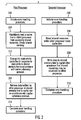
- FIG. 2 illustrates an embodiment in which operations of processors of a multiprocessor system may be coordinated using a processor cache, a shared memory and a cache coherency protocol.
- the bridge 36a of the processing complex 8a may fail.
- one of the caches 28a, 28b may be utilized with the shared memory 30a and a cache coherency protocol.
- the shared resource such as the bridge 36a may issue interrupts to each of the processors 10a, 10b, upon entering an error condition.
- a first processor such as the processor 10a may initiate (block 200) an error handling procedure.
- a second processor such as the processor 10b may initiate (block 202) a second error handling procedure.
- other events may be utilized by the processors 10a, 10b to initiate error handling procedures.
- the processors 10a, 10b may monitor the status of various shared devices and initiate error handling procedures upon detection of an error status.
- the first processor 10a repetitively reads (block 204) a cache line such as a line of the cache 28a.
- the repetitive cache line reading occupies the first processor 10a and inhibits the first processor 10a from accessing the shared resources including the bridge 36a. This repetitive reading may be achieved using a loop process, for example.
- the cache line being repetitively read by the first processor 10a is cached from a line of a shared memory of resources shared by both the first processor 10a and the second processor 10b.
- the cache line may be cached from a line of the shared memory 30a.
- coherency is maintained between the shared memory line and the cache line in accordance with a cache coherency protocol such as the MESI, protocol, for example.
- MESI cache coherency protocol
- the state of the cache line being read becomes Exclusive to the first processor 10a. It is appreciated that other cache coherency protocols may be utilized as well.
- the first processor 10a also snoops (block 204) the shared memory 30a via the shared bus 31a to identify changes to the cached memory line from the shared memory 30a.
- the second processor 10b in executing its error handling procedure, can safely reset (block 206) a shared resource such as the bridge 36a without interference from the first processor 10a. It is appreciated that the error handling procedures which can be undertaken by the second processor 10b while the first processor 10a is inhibited from accessing a shared resource can include other actions such as fencing off a failed resource or taking other action to restore a failed resource.
- the second processor 10b may write (block 208) data to the shared memory line of the shared memory 30a, which shared memory line has been cached by the first processor cache 28a.
- this data write by the second processor 10b may be used to provide a signal to the first processor 10a that it is safe for the first processor to resume accessing the shared resource.
- one appropriate time for the second processor 10b to write data to the shared memory line of the shared memory 30a may be upon completion of the bridge 36a resetting operations by the second processor 10b which resulted in a successful restoration of the shared resource or at least a portion of the shared resource or resources.
- the second processor 10b may complete (block 210) its error handling procedure. It is appreciated that the write to the cached memory line in the shared memory 30aby the second processor 10b may be done to signal other information to the other processor 10a and may be done at other times, depending upon the particular application.
- the first processor 10a snooping the shared memory 30a via the shared bus 31a detects this write to the cached memory line in the shared memory 30a by the second processor 10b.
- the first processor 10a changes (block 212) the state of the cache line in the cache 28a in response to the data write to the shared memory line in the shared memory 30a by the second processor 10b.
- the state of the cache memory line in the first processor cache 28a is changed to the Invalid state.
- the first processor 10a may leave a loop process of repetitively reading the memory line in the cache 28a and retrieve (block 214) the updated data written to the cached memory line in the shared memory 30a. If the failed resource is a bridge to the shared memory 30a, for example, the shared resource will have been restored by the second processor 10b such that the first processor 10a can safely access the restored shared resources.
- the first processor completes (block 216) its error handling procedure. If the second processor 10b has fully restored the system of all error states, the first processor can resume its normal processing. In another example, the restoration operations of the second processor may be incomplete. In this example, the processors 10a and 10b can switch roles and resume the restoration process. Thus the processor 10b may be designed the "first processor" of FIG. 2 and the processor 10a may be designated the "second processor" of FIG. 2 .
- the first processor 10b repetitively reads (block 204) a cache line such as a line of the cache 28b.
- the repetitive cache line reading occupies the first processor 10b and inhibits the first processor 10b from accessing the shared resources including the bridge 36a.
- the second processor 10a in executing its error handling procedure, can safely reset (block 206) a shared resource such as the bridge 36a without interference from the first processor 10b.
- the second processor 10a may write (block 208) data to the shared memory line of the shared memory 30a, which shared memory line has been cached by the first processor cache 28b, to signal the other processor 10b that it may safely access the shared resource, and the second processor 10a may complete (block 210) its error handling procedure.
- the first processor 10b snooping the shared memory 30a via the shared bus 31a detects this write to the cached memory line in the shared memory 30a by the second processor 10a.
- the first processor 10b changes (block 212) the state of the cache line in the cache 2 8b to the invalid state in response to the data write to the shared memory line in the shared memory 30a by the second processor 10a.
- the first processor 10b may leave a loop process of repetitively reading the memory line in the cache 28b and retrieve (block 214) the updated data written to the cached memory line in the shared memory 30a. If the failed resource is a bridge to the shared memory 30a, for example, the shared resource will have been restored by the second processor 10a such that the first processor 10b can safely access the restored shared resources.
- the first processor 10b completes (block 216) its error handling procedure. If the second processor 10a has fully restored the system of all error states, the first processor 10b can resume its normal processing. In another example, the restoration operations of the second processor 10a may still be incomplete. In this example, the processors 10a and 10b can again switch roles to complete the restoration or other process.
- a time limit may be set for each processor to repetitively read a cache line (block 204). For example, if a time limit expires before the cache line state changes from Exclusive state to the Invalid state, the first processor may, in one embodiment, assume the other, second processor is dead. If so the first processor can take over the role of the second processor and execute the second processor recovery procedure including resetting the shared resource (block 206).
- a shared resource such as the bridge 36b of the processing complex 8b may fail.
- one of the caches 28c, 28d may be utilized with the shared memory 30b and a cache coherency protocol.
- the described embodiments may be implemented as a method, apparatus or article of manufacture using standard programming and/or engineering techniques to produce software, firmware, hardware, or any combination thereof.
- article of manufacture refers to code or logic implemented in hardware logic (e.g., an integrated circuit chip, Programmable Gate Array (PGA), Application Specific Integrated Circuit (ASIC), etc.) or a computer readable medium, such as magnetic storage medium (e.g., hard disk drives, floppy disks,, tape, etc.), optical storage (CD-ROMs, optical disks, etc.), volatile and non-volatile memory devices (e.g., EEPROMs, ROMs, PROMs, RAMs, DRAMs, SRAMs, firmware, programmable logic, etc.).
- Code in the computer readable medium is accessed and executed by a processor.
- the code in which preferred embodiments are implemented may further be accessible through a transmission media or from a file server over a network.
- the article of manufacture in which the code is implemented may comprise a transmission media, such as a network transmission line, wireless transmission media, signals propagating through space, radio waves, infrared signals, etc.
- the "article of manufacture” may comprise the medium in which the code is embodied.
- the “article of manufacture” may comprise a combination of hardware and software components in which the code is embodied, processed, and executed.
- Certain embodiments may be directed to a method for deploying computing instruction by a person or automated processing integrating computer-readable code into a computing system, wherein the code in combination with the computing system is enabled to perform the operations of the described embodiments.
- the supervisor manages the execution of different logical partitions.
- the supervisor module may comprise an intermediate device driver and an operating system which may be a different type from the operating system of the other processing complex or may be the same, depending upon the particular application.
- control unit 6 included two processing complexes 8a, 8b. In additional embodiments, there may be more than two systems accessing a shared device. In such embodiments, the device driver 20a receiving the interrupt may communicate with multiple processing complexes to coordinate restoration or other operations.
- FIG. 2 show certain events occurring in a certain order. In alternative embodiments, certain operations may be performed in a different order, modified or removed. Moreover, steps may be added to the above described logic and still conform to the described embodiments. Further, operations described herein may occur sequentially or certain operations may be processed in parallel. Yet further, operations may be performed by a single processing unit or by distributed processing units.
Landscapes
- Engineering & Computer Science (AREA)
- Theoretical Computer Science (AREA)
- Physics & Mathematics (AREA)
- General Engineering & Computer Science (AREA)
- General Physics & Mathematics (AREA)
- Memory System Of A Hierarchy Structure (AREA)
- Saccharide Compounds (AREA)
- Hardware Redundancy (AREA)
Applications Claiming Priority (2)
| Application Number | Priority Date | Filing Date | Title |
|---|---|---|---|
| US11/001,476 US7418557B2 (en) | 2004-11-30 | 2004-11-30 | Managing multiprocessor operations |
| PCT/EP2005/055907 WO2006058826A1 (en) | 2004-11-30 | 2005-11-11 | Managing multiprocessor operations |
Publications (2)
| Publication Number | Publication Date |
|---|---|
| EP1839156A1 EP1839156A1 (en) | 2007-10-03 |
| EP1839156B1 true EP1839156B1 (en) | 2008-07-23 |
Family
ID=35645753
Family Applications (1)
| Application Number | Title | Priority Date | Filing Date |
|---|---|---|---|
| EP05808157A Active EP1839156B1 (en) | 2004-11-30 | 2005-11-11 | Managing multiprocessor operations |
Country Status (9)
Cited By (1)
| Publication number | Priority date | Publication date | Assignee | Title |
|---|---|---|---|---|
| US10915445B2 (en) | 2018-09-18 | 2021-02-09 | Nvidia Corporation | Coherent caching of data for high bandwidth scaling |
Families Citing this family (16)
| Publication number | Priority date | Publication date | Assignee | Title |
|---|---|---|---|---|
| US7536694B2 (en) * | 2004-11-30 | 2009-05-19 | International Business Machines Corporation | Exception handling in a multiprocessor system |
| US7937709B2 (en) | 2004-12-29 | 2011-05-03 | Intel Corporation | Synchronizing multiple threads efficiently |
| JP2006227856A (ja) * | 2005-02-17 | 2006-08-31 | Hitachi Ltd | アクセス制御装置及びそれに搭載されるインターフェース |
| US7818056B2 (en) * | 2005-03-24 | 2010-10-19 | Cardiac Pacemakers, Inc. | Blending cardiac rhythm detection processes |
| JP4831599B2 (ja) * | 2005-06-28 | 2011-12-07 | ルネサスエレクトロニクス株式会社 | 処理装置 |
| US7849362B2 (en) * | 2005-12-09 | 2010-12-07 | International Business Machines Corporation | Method and system of coherent design verification of inter-cluster interactions |
| JP2007219571A (ja) * | 2006-02-14 | 2007-08-30 | Hitachi Ltd | 記憶制御装置及びストレージシステム |
| JP5387776B2 (ja) * | 2010-07-27 | 2014-01-15 | 富士通株式会社 | 割込制御方法、マルチコアプロセッサシステム、および割込制御プログラム |
| JP5745868B2 (ja) * | 2011-01-18 | 2015-07-08 | トヨタ自動車株式会社 | マルチプロセッサシステム |
| JP5614419B2 (ja) * | 2012-02-29 | 2014-10-29 | 富士通株式会社 | 情報処理装置、制御方法および制御プログラム |
| WO2013159288A1 (en) * | 2012-04-25 | 2013-10-31 | Intel Corporation | Method and system for maintaining release consistency in shared memory programming |
| US9135175B2 (en) * | 2012-12-21 | 2015-09-15 | Oracle International Corporation | Distributed cache coherency directory with failure redundancy |
| CN103745315A (zh) * | 2013-12-31 | 2014-04-23 | 太原理工大学 | 重点项目行政执法监察联动管理方法及系统 |
| US10310982B2 (en) * | 2016-12-15 | 2019-06-04 | International Business Machines Corporation | Target cache line arbitration within a processor cluster |
| US10339064B2 (en) * | 2017-03-29 | 2019-07-02 | International Business Machines Corporation | Hot cache line arbitration |
| CN114327920B (zh) * | 2022-03-16 | 2022-06-21 | 长沙金维信息技术有限公司 | 用于多处理器系统的硬件资源共享方法 |
Family Cites Families (9)
| Publication number | Priority date | Publication date | Assignee | Title |
|---|---|---|---|---|
| JPH08202622A (ja) * | 1995-01-31 | 1996-08-09 | Fujitsu Ltd | 分散型メモリ構成のキャッシュ制御方法 |
| US5930821A (en) * | 1997-05-12 | 1999-07-27 | Integrated Device Technology, Inc. | Method and apparatus for shared cache lines in split data/code caches |
| US6314526B1 (en) | 1998-07-10 | 2001-11-06 | International Business Machines Corporation | Resource group quorum scheme for highly scalable and highly available cluster system management |
| US6467050B1 (en) | 1998-09-14 | 2002-10-15 | International Business Machines Corporation | Method and apparatus for managing services within a cluster computer system |
| JP3676934B2 (ja) * | 1998-12-15 | 2005-07-27 | 株式会社日立製作所 | プロセッサおよびマルチプロセッサシステム |
| US6622260B1 (en) | 1999-12-30 | 2003-09-16 | Suresh Marisetty | System abstraction layer, processor abstraction layer, and operating system error handling |
| US6751705B1 (en) | 2000-08-25 | 2004-06-15 | Silicon Graphics, Inc. | Cache line converter |
| US6772298B2 (en) * | 2000-12-20 | 2004-08-03 | Intel Corporation | Method and apparatus for invalidating a cache line without data return in a multi-node architecture |
| US6859866B2 (en) | 2001-10-01 | 2005-02-22 | International Business Machines Corporation | Synchronizing processing of commands invoked against duplexed coupling facility structures |
-
2004
- 2004-11-30 US US11/001,476 patent/US7418557B2/en not_active Expired - Fee Related
-
2005
- 2005-11-11 WO PCT/EP2005/055907 patent/WO2006058826A1/en active IP Right Grant
- 2005-11-11 EP EP05808157A patent/EP1839156B1/en active Active
- 2005-11-11 DE DE602005008477T patent/DE602005008477D1/de active Active
- 2005-11-11 CN CNB2005800406226A patent/CN100568199C/zh not_active Expired - Fee Related
- 2005-11-11 JP JP2007541929A patent/JP4641545B2/ja not_active Expired - Fee Related
- 2005-11-11 AT AT05808157T patent/ATE402444T1/de not_active IP Right Cessation
- 2005-11-11 MX MX2007006350A patent/MX2007006350A/es active IP Right Grant
-
2007
- 2007-05-28 IL IL183470A patent/IL183470A/en not_active IP Right Cessation
-
2008
- 2008-03-20 US US12/052,569 patent/US7650467B2/en not_active Expired - Fee Related
Cited By (1)
| Publication number | Priority date | Publication date | Assignee | Title |
|---|---|---|---|---|
| US10915445B2 (en) | 2018-09-18 | 2021-02-09 | Nvidia Corporation | Coherent caching of data for high bandwidth scaling |
Also Published As
| Publication number | Publication date |
|---|---|
| US20060117147A1 (en) | 2006-06-01 |
| DE602005008477D1 (de) | 2008-09-04 |
| CN101065736A (zh) | 2007-10-31 |
| US7418557B2 (en) | 2008-08-26 |
| US20080168238A1 (en) | 2008-07-10 |
| ATE402444T1 (de) | 2008-08-15 |
| EP1839156A1 (en) | 2007-10-03 |
| MX2007006350A (es) | 2007-06-19 |
| JP2008522264A (ja) | 2008-06-26 |
| US7650467B2 (en) | 2010-01-19 |
| WO2006058826A1 (en) | 2006-06-08 |
| IL183470A0 (en) | 2007-09-20 |
| JP4641545B2 (ja) | 2011-03-02 |
| IL183470A (en) | 2011-03-31 |
| CN100568199C (zh) | 2009-12-09 |
Similar Documents
| Publication | Publication Date | Title |
|---|---|---|
| US7650467B2 (en) | Coordination of multiprocessor operations with shared resources | |
| US5423044A (en) | Shared, distributed lock manager for loosely coupled processing systems | |
| US9575905B2 (en) | Storage controller cache synchronization method and apparatus | |
| US6912621B2 (en) | Method and apparatus for updating data in mass storage subsystem using emulated shared memory | |
| US6449699B2 (en) | Apparatus and method for partitioned memory protection in cache coherent symmetric multiprocessor systems | |
| EP1426863B1 (en) | Method and apparatus for maintaining consistency of data stored in a group of mirroring devices | |
| US7024530B2 (en) | Method, system, and program for establishing and using a point-in-time copy relationship | |
| US20050132249A1 (en) | Apparatus method and system for fault tolerant virtual memory management | |
| US20040267706A1 (en) | Method, system, and program for managing requests to tracks subject to a relationship | |
| JP2003162447A (ja) | エラー回復 | |
| EP2382544B1 (en) | Determining modified data in cache for use during a recovery operation | |
| JP2002229837A (ja) | 共有ディスク・パラレル・データ・ファイル内のデータに対するアクセスを制御する方法 | |
| US7409722B2 (en) | Control status register access to enable domain reconfiguration | |
| US7536694B2 (en) | Exception handling in a multiprocessor system | |
| US10635552B1 (en) | Method for tracking validity of journal copies to allow journal mirroring | |
| US20060106996A1 (en) | Updating data shared among systems | |
| US11016896B2 (en) | Reducing overhead of managing cache areas | |
| US10789168B2 (en) | Maintaining multiple cache areas | |
| US10795814B2 (en) | Placement of local cache areas | |
| JP2716571B2 (ja) | 二重化データ保全装置 | |
| JPH0312773A (ja) | データベース処理における局所異常回復処理方式 | |
| JPH0795311B2 (ja) | 二重化処理装置 | |
| JPH06124242A (ja) | 二重化共有メモリ等価性保証方式 |
Legal Events
| Date | Code | Title | Description |
|---|---|---|---|
| PUAI | Public reference made under article 153(3) epc to a published international application that has entered the european phase |
Free format text: ORIGINAL CODE: 0009012 |
|
| 17P | Request for examination filed |
Effective date: 20070627 |
|
| AK | Designated contracting states |
Kind code of ref document: A1 Designated state(s): AT BE BG CH CY CZ DE DK EE ES FI FR GB GR HU IE IS IT LI LT LU LV MC NL PL PT RO SE SI SK TR |
|
| RIN1 | Information on inventor provided before grant (corrected) |
Inventor name: SONG, CHENG-CHUNG Inventor name: RANKIN, RICKY DEANIBM UNITED KINGDOM LIMITED Inventor name: MIRABEAU, LUCIEN Inventor name: HSU, YU-CHENG Inventor name: BLINICK, STEPHEN LAROUX |
|
| GRAP | Despatch of communication of intention to grant a patent |
Free format text: ORIGINAL CODE: EPIDOSNIGR1 |
|
| DAX | Request for extension of the european patent (deleted) | ||
| GRAS | Grant fee paid |
Free format text: ORIGINAL CODE: EPIDOSNIGR3 |
|
| GRAA | (expected) grant |
Free format text: ORIGINAL CODE: 0009210 |
|
| AK | Designated contracting states |
Kind code of ref document: B1 Designated state(s): AT BE BG CH CY CZ DE DK EE ES FI FR GB GR HU IE IS IT LI LT LU LV MC NL PL PT RO SE SI SK TR |
|
| REG | Reference to a national code |
Ref country code: GB Ref legal event code: FG4D |
|
| REG | Reference to a national code |
Ref country code: CH Ref legal event code: NV Representative=s name: IBM RESEARCH GMBH ZURICH RESEARCH LABORATORY INTEL Ref country code: CH Ref legal event code: EP |
|
| REG | Reference to a national code |
Ref country code: IE Ref legal event code: FG4D |
|
| REF | Corresponds to: |
Ref document number: 602005008477 Country of ref document: DE Date of ref document: 20080904 Kind code of ref document: P |
|
| NLV1 | Nl: lapsed or annulled due to failure to fulfill the requirements of art. 29p and 29m of the patents act | ||
| PG25 | Lapsed in a contracting state [announced via postgrant information from national office to epo] |
Ref country code: NL Free format text: LAPSE BECAUSE OF FAILURE TO SUBMIT A TRANSLATION OF THE DESCRIPTION OR TO PAY THE FEE WITHIN THE PRESCRIBED TIME-LIMIT Effective date: 20080723 Ref country code: LT Free format text: LAPSE BECAUSE OF FAILURE TO SUBMIT A TRANSLATION OF THE DESCRIPTION OR TO PAY THE FEE WITHIN THE PRESCRIBED TIME-LIMIT Effective date: 20080723 Ref country code: IS Free format text: LAPSE BECAUSE OF FAILURE TO SUBMIT A TRANSLATION OF THE DESCRIPTION OR TO PAY THE FEE WITHIN THE PRESCRIBED TIME-LIMIT Effective date: 20081123 |
|
| PG25 | Lapsed in a contracting state [announced via postgrant information from national office to epo] |
Ref country code: SI Free format text: LAPSE BECAUSE OF FAILURE TO SUBMIT A TRANSLATION OF THE DESCRIPTION OR TO PAY THE FEE WITHIN THE PRESCRIBED TIME-LIMIT Effective date: 20080723 Ref country code: PT Free format text: LAPSE BECAUSE OF FAILURE TO SUBMIT A TRANSLATION OF THE DESCRIPTION OR TO PAY THE FEE WITHIN THE PRESCRIBED TIME-LIMIT Effective date: 20081223 Ref country code: LV Free format text: LAPSE BECAUSE OF FAILURE TO SUBMIT A TRANSLATION OF THE DESCRIPTION OR TO PAY THE FEE WITHIN THE PRESCRIBED TIME-LIMIT Effective date: 20080723 Ref country code: FI Free format text: LAPSE BECAUSE OF FAILURE TO SUBMIT A TRANSLATION OF THE DESCRIPTION OR TO PAY THE FEE WITHIN THE PRESCRIBED TIME-LIMIT Effective date: 20080723 Ref country code: ES Free format text: LAPSE BECAUSE OF FAILURE TO SUBMIT A TRANSLATION OF THE DESCRIPTION OR TO PAY THE FEE WITHIN THE PRESCRIBED TIME-LIMIT Effective date: 20081103 Ref country code: BG Free format text: LAPSE BECAUSE OF FAILURE TO SUBMIT A TRANSLATION OF THE DESCRIPTION OR TO PAY THE FEE WITHIN THE PRESCRIBED TIME-LIMIT Effective date: 20081023 Ref country code: AT Free format text: LAPSE BECAUSE OF FAILURE TO SUBMIT A TRANSLATION OF THE DESCRIPTION OR TO PAY THE FEE WITHIN THE PRESCRIBED TIME-LIMIT Effective date: 20080723 |
|
| PG25 | Lapsed in a contracting state [announced via postgrant information from national office to epo] |
Ref country code: BE Free format text: LAPSE BECAUSE OF FAILURE TO SUBMIT A TRANSLATION OF THE DESCRIPTION OR TO PAY THE FEE WITHIN THE PRESCRIBED TIME-LIMIT Effective date: 20080723 |
|
| PG25 | Lapsed in a contracting state [announced via postgrant information from national office to epo] |
Ref country code: EE Free format text: LAPSE BECAUSE OF FAILURE TO SUBMIT A TRANSLATION OF THE DESCRIPTION OR TO PAY THE FEE WITHIN THE PRESCRIBED TIME-LIMIT Effective date: 20080723 Ref country code: DK Free format text: LAPSE BECAUSE OF FAILURE TO SUBMIT A TRANSLATION OF THE DESCRIPTION OR TO PAY THE FEE WITHIN THE PRESCRIBED TIME-LIMIT Effective date: 20080723 |
|
| PG25 | Lapsed in a contracting state [announced via postgrant information from national office to epo] |
Ref country code: SK Free format text: LAPSE BECAUSE OF FAILURE TO SUBMIT A TRANSLATION OF THE DESCRIPTION OR TO PAY THE FEE WITHIN THE PRESCRIBED TIME-LIMIT Effective date: 20080723 Ref country code: RO Free format text: LAPSE BECAUSE OF FAILURE TO SUBMIT A TRANSLATION OF THE DESCRIPTION OR TO PAY THE FEE WITHIN THE PRESCRIBED TIME-LIMIT Effective date: 20080723 Ref country code: CZ Free format text: LAPSE BECAUSE OF FAILURE TO SUBMIT A TRANSLATION OF THE DESCRIPTION OR TO PAY THE FEE WITHIN THE PRESCRIBED TIME-LIMIT Effective date: 20080723 |
|
| PLBE | No opposition filed within time limit |
Free format text: ORIGINAL CODE: 0009261 |
|
| STAA | Information on the status of an ep patent application or granted ep patent |
Free format text: STATUS: NO OPPOSITION FILED WITHIN TIME LIMIT |
|
| PG25 | Lapsed in a contracting state [announced via postgrant information from national office to epo] |
Ref country code: MC Free format text: LAPSE BECAUSE OF NON-PAYMENT OF DUE FEES Effective date: 20081130 |
|
| 26N | No opposition filed |
Effective date: 20090424 |
|
| PG25 | Lapsed in a contracting state [announced via postgrant information from national office to epo] |
Ref country code: IT Free format text: LAPSE BECAUSE OF FAILURE TO SUBMIT A TRANSLATION OF THE DESCRIPTION OR TO PAY THE FEE WITHIN THE PRESCRIBED TIME-LIMIT Effective date: 20080723 |
|
| PG25 | Lapsed in a contracting state [announced via postgrant information from national office to epo] |
Ref country code: IE Free format text: LAPSE BECAUSE OF NON-PAYMENT OF DUE FEES Effective date: 20081111 |
|
| REG | Reference to a national code |
Ref country code: GB Ref legal event code: 746 Effective date: 20091016 |
|
| PG25 | Lapsed in a contracting state [announced via postgrant information from national office to epo] |
Ref country code: SE Free format text: LAPSE BECAUSE OF FAILURE TO SUBMIT A TRANSLATION OF THE DESCRIPTION OR TO PAY THE FEE WITHIN THE PRESCRIBED TIME-LIMIT Effective date: 20081023 |
|
| PG25 | Lapsed in a contracting state [announced via postgrant information from national office to epo] |
Ref country code: PL Free format text: LAPSE BECAUSE OF FAILURE TO SUBMIT A TRANSLATION OF THE DESCRIPTION OR TO PAY THE FEE WITHIN THE PRESCRIBED TIME-LIMIT Effective date: 20080723 |
|
| REG | Reference to a national code |
Ref country code: CH Ref legal event code: PL |
|
| PG25 | Lapsed in a contracting state [announced via postgrant information from national office to epo] |
Ref country code: LU Free format text: LAPSE BECAUSE OF NON-PAYMENT OF DUE FEES Effective date: 20081111 Ref country code: HU Free format text: LAPSE BECAUSE OF FAILURE TO SUBMIT A TRANSLATION OF THE DESCRIPTION OR TO PAY THE FEE WITHIN THE PRESCRIBED TIME-LIMIT Effective date: 20090124 Ref country code: CY Free format text: LAPSE BECAUSE OF FAILURE TO SUBMIT A TRANSLATION OF THE DESCRIPTION OR TO PAY THE FEE WITHIN THE PRESCRIBED TIME-LIMIT Effective date: 20080723 |
|
| PG25 | Lapsed in a contracting state [announced via postgrant information from national office to epo] |
Ref country code: TR Free format text: LAPSE BECAUSE OF FAILURE TO SUBMIT A TRANSLATION OF THE DESCRIPTION OR TO PAY THE FEE WITHIN THE PRESCRIBED TIME-LIMIT Effective date: 20080723 |
|
| PG25 | Lapsed in a contracting state [announced via postgrant information from national office to epo] |
Ref country code: LI Free format text: LAPSE BECAUSE OF NON-PAYMENT OF DUE FEES Effective date: 20091130 Ref country code: GR Free format text: LAPSE BECAUSE OF FAILURE TO SUBMIT A TRANSLATION OF THE DESCRIPTION OR TO PAY THE FEE WITHIN THE PRESCRIBED TIME-LIMIT Effective date: 20081024 Ref country code: CH Free format text: LAPSE BECAUSE OF NON-PAYMENT OF DUE FEES Effective date: 20091130 |
|
| REG | Reference to a national code |
Ref country code: FR Ref legal event code: PLFP Year of fee payment: 11 |
|
| REG | Reference to a national code |
Ref country code: FR Ref legal event code: PLFP Year of fee payment: 12 |
|
| REG | Reference to a national code |
Ref country code: FR Ref legal event code: PLFP Year of fee payment: 13 |
|
| REG | Reference to a national code |
Ref country code: DE Ref legal event code: R082 Ref document number: 602005008477 Country of ref document: DE Representative=s name: KUISMA, SIRPA, FI |
|
| PGFP | Annual fee paid to national office [announced via postgrant information from national office to epo] |
Ref country code: DE Payment date: 20220922 Year of fee payment: 18 |
|
| P01 | Opt-out of the competence of the unified patent court (upc) registered |
Effective date: 20230423 |
|
| REG | Reference to a national code |
Ref country code: DE Ref legal event code: R119 Ref document number: 602005008477 Country of ref document: DE |
|
| PG25 | Lapsed in a contracting state [announced via postgrant information from national office to epo] |
Ref country code: DE Free format text: LAPSE BECAUSE OF NON-PAYMENT OF DUE FEES Effective date: 20240601 |
|
| PG25 | Lapsed in a contracting state [announced via postgrant information from national office to epo] |
Ref country code: DE Free format text: LAPSE BECAUSE OF NON-PAYMENT OF DUE FEES Effective date: 20240601 |
|
| PGFP | Annual fee paid to national office [announced via postgrant information from national office to epo] |
Ref country code: GB Payment date: 20241122 Year of fee payment: 20 |
|
| PGFP | Annual fee paid to national office [announced via postgrant information from national office to epo] |
Ref country code: FR Payment date: 20241108 Year of fee payment: 20 |