EP1835543A1 - Method for manufacturing semiconductor device - Google Patents
Method for manufacturing semiconductor device Download PDFInfo
- Publication number
- EP1835543A1 EP1835543A1 EP06005196A EP06005196A EP1835543A1 EP 1835543 A1 EP1835543 A1 EP 1835543A1 EP 06005196 A EP06005196 A EP 06005196A EP 06005196 A EP06005196 A EP 06005196A EP 1835543 A1 EP1835543 A1 EP 1835543A1
- Authority
- EP
- European Patent Office
- Prior art keywords
- hetero
- region
- semiconductor
- hetero semiconductor
- manufacturing
- Prior art date
- Legal status (The legal status is an assumption and is not a legal conclusion. Google has not performed a legal analysis and makes no representation as to the accuracy of the status listed.)
- Granted
Links
- 239000004065 semiconductor Substances 0.000 title claims abstract description 229
- 238000000034 method Methods 0.000 title claims abstract description 58
- 238000004519 manufacturing process Methods 0.000 title claims abstract description 44
- 125000005842 heteroatom Chemical group 0.000 claims abstract description 159
- 230000008569 process Effects 0.000 claims abstract description 42
- 238000000059 patterning Methods 0.000 claims abstract description 8
- 239000010410 layer Substances 0.000 claims description 58
- 229910021420 polycrystalline silicon Inorganic materials 0.000 claims description 38
- HBMJWWWQQXIZIP-UHFFFAOYSA-N silicon carbide Chemical compound [Si+]#[C-] HBMJWWWQQXIZIP-UHFFFAOYSA-N 0.000 claims description 35
- 229910010271 silicon carbide Inorganic materials 0.000 claims description 34
- 239000000463 material Substances 0.000 claims description 18
- 238000005530 etching Methods 0.000 claims description 17
- 230000003647 oxidation Effects 0.000 claims description 12
- 238000007254 oxidation reaction Methods 0.000 claims description 12
- 229910021419 crystalline silicon Inorganic materials 0.000 claims description 4
- 238000005498 polishing Methods 0.000 claims description 4
- 239000000126 substance Substances 0.000 claims description 4
- 229910021417 amorphous silicon Inorganic materials 0.000 claims description 2
- 239000011229 interlayer Substances 0.000 claims description 2
- 239000003963 antioxidant agent Substances 0.000 description 21
- 230000003078 antioxidant effect Effects 0.000 description 21
- 239000000758 substrate Substances 0.000 description 18
- PXHVJJICTQNCMI-UHFFFAOYSA-N Nickel Chemical compound [Ni] PXHVJJICTQNCMI-UHFFFAOYSA-N 0.000 description 15
- XHXFXVLFKHQFAL-UHFFFAOYSA-N phosphoryl trichloride Chemical compound ClP(Cl)(Cl)=O XHXFXVLFKHQFAL-UHFFFAOYSA-N 0.000 description 14
- 230000004888 barrier function Effects 0.000 description 13
- 239000002772 conduction electron Substances 0.000 description 12
- 239000010936 titanium Substances 0.000 description 12
- 238000010586 diagram Methods 0.000 description 10
- XUIMIQQOPSSXEZ-UHFFFAOYSA-N Silicon Chemical compound [Si] XUIMIQQOPSSXEZ-UHFFFAOYSA-N 0.000 description 9
- 229910052710 silicon Inorganic materials 0.000 description 9
- 239000010703 silicon Substances 0.000 description 9
- 230000005684 electric field Effects 0.000 description 8
- 150000004767 nitrides Chemical class 0.000 description 8
- OAICVXFJPJFONN-UHFFFAOYSA-N Phosphorus Chemical compound [P] OAICVXFJPJFONN-UHFFFAOYSA-N 0.000 description 7
- 229910052698 phosphorus Inorganic materials 0.000 description 7
- 239000011574 phosphorus Substances 0.000 description 7
- KRHYYFGTRYWZRS-UHFFFAOYSA-N Fluorane Chemical compound F KRHYYFGTRYWZRS-UHFFFAOYSA-N 0.000 description 6
- RTAQQCXQSZGOHL-UHFFFAOYSA-N Titanium Chemical compound [Ti] RTAQQCXQSZGOHL-UHFFFAOYSA-N 0.000 description 6
- 238000002513 implantation Methods 0.000 description 6
- 229910052719 titanium Inorganic materials 0.000 description 6
- 238000009792 diffusion process Methods 0.000 description 5
- 238000001312 dry etching Methods 0.000 description 5
- 239000012535 impurity Substances 0.000 description 5
- 238000004518 low pressure chemical vapour deposition Methods 0.000 description 5
- 229910052759 nickel Inorganic materials 0.000 description 5
- 238000000206 photolithography Methods 0.000 description 5
- 239000007790 solid phase Substances 0.000 description 5
- 238000001039 wet etching Methods 0.000 description 4
- DDFHBQSCUXNBSA-UHFFFAOYSA-N 5-(5-carboxythiophen-2-yl)thiophene-2-carboxylic acid Chemical compound S1C(C(=O)O)=CC=C1C1=CC=C(C(O)=O)S1 DDFHBQSCUXNBSA-UHFFFAOYSA-N 0.000 description 3
- 229910052581 Si3N4 Inorganic materials 0.000 description 3
- 238000000151 deposition Methods 0.000 description 3
- 239000011259 mixed solution Substances 0.000 description 3
- HQVNEWCFYHHQES-UHFFFAOYSA-N silicon nitride Chemical compound N12[Si]34N5[Si]62N3[Si]51N64 HQVNEWCFYHHQES-UHFFFAOYSA-N 0.000 description 3
- NBIIXXVUZAFLBC-UHFFFAOYSA-N Phosphoric acid Chemical compound OP(O)(O)=O NBIIXXVUZAFLBC-UHFFFAOYSA-N 0.000 description 2
- VYPSYNLAJGMNEJ-UHFFFAOYSA-N Silicium dioxide Chemical compound O=[Si]=O VYPSYNLAJGMNEJ-UHFFFAOYSA-N 0.000 description 2
- 238000009825 accumulation Methods 0.000 description 2
- 230000004913 activation Effects 0.000 description 2
- 229910052782 aluminium Inorganic materials 0.000 description 2
- -1 aluminum ion Chemical class 0.000 description 2
- 238000001704 evaporation Methods 0.000 description 2
- 238000010438 heat treatment Methods 0.000 description 2
- 238000005224 laser annealing Methods 0.000 description 2
- 230000004048 modification Effects 0.000 description 2
- 238000012986 modification Methods 0.000 description 2
- 238000001451 molecular beam epitaxy Methods 0.000 description 2
- 238000001020 plasma etching Methods 0.000 description 2
- 229910052814 silicon oxide Inorganic materials 0.000 description 2
- 239000000243 solution Substances 0.000 description 2
- 238000004544 sputter deposition Methods 0.000 description 2
- 229910002601 GaN Inorganic materials 0.000 description 1
- JMASRVWKEDWRBT-UHFFFAOYSA-N Gallium nitride Chemical compound [Ga]#N JMASRVWKEDWRBT-UHFFFAOYSA-N 0.000 description 1
- 229910019142 PO4 Inorganic materials 0.000 description 1
- 229910000577 Silicon-germanium Inorganic materials 0.000 description 1
- LEVVHYCKPQWKOP-UHFFFAOYSA-N [Si].[Ge] Chemical compound [Si].[Ge] LEVVHYCKPQWKOP-UHFFFAOYSA-N 0.000 description 1
- XAGFODPZIPBFFR-UHFFFAOYSA-N aluminium Chemical compound [Al] XAGFODPZIPBFFR-UHFFFAOYSA-N 0.000 description 1
- 229910000147 aluminium phosphate Inorganic materials 0.000 description 1
- 229910052796 boron Inorganic materials 0.000 description 1
- 230000008859 change Effects 0.000 description 1
- 230000000994 depressogenic effect Effects 0.000 description 1
- 229910003460 diamond Inorganic materials 0.000 description 1
- 239000010432 diamond Substances 0.000 description 1
- 230000005669 field effect Effects 0.000 description 1
- 239000011521 glass Substances 0.000 description 1
- 230000006872 improvement Effects 0.000 description 1
- 239000007800 oxidant agent Substances 0.000 description 1
- 230000001590 oxidative effect Effects 0.000 description 1
- NBIIXXVUZAFLBC-UHFFFAOYSA-K phosphate Chemical compound [O-]P([O-])([O-])=O NBIIXXVUZAFLBC-UHFFFAOYSA-K 0.000 description 1
- 239000010452 phosphate Substances 0.000 description 1
- 238000011084 recovery Methods 0.000 description 1
- 238000010992 reflux Methods 0.000 description 1
- 239000002210 silicon-based material Substances 0.000 description 1
- 239000002344 surface layer Substances 0.000 description 1
- 230000005641 tunneling Effects 0.000 description 1
Images


Classifications
-
- H—ELECTRICITY
- H01—ELECTRIC ELEMENTS
- H01L—SEMICONDUCTOR DEVICES NOT COVERED BY CLASS H10
- H01L29/00—Semiconductor devices specially adapted for rectifying, amplifying, oscillating or switching and having potential barriers; Capacitors or resistors having potential barriers, e.g. a PN-junction depletion layer or carrier concentration layer; Details of semiconductor bodies or of electrodes thereof ; Multistep manufacturing processes therefor
- H01L29/66—Types of semiconductor device ; Multistep manufacturing processes therefor
- H01L29/68—Types of semiconductor device ; Multistep manufacturing processes therefor controllable by only the electric current supplied, or only the electric potential applied, to an electrode which does not carry the current to be rectified, amplified or switched
- H01L29/76—Unipolar devices, e.g. field effect transistors
- H01L29/772—Field effect transistors
- H01L29/78—Field effect transistors with field effect produced by an insulated gate
- H01L29/7827—Vertical transistors
- H01L29/7828—Vertical transistors without inversion channel, e.g. vertical ACCUFETs, normally-on vertical MISFETs
-
- H—ELECTRICITY
- H01—ELECTRIC ELEMENTS
- H01L—SEMICONDUCTOR DEVICES NOT COVERED BY CLASS H10
- H01L29/00—Semiconductor devices specially adapted for rectifying, amplifying, oscillating or switching and having potential barriers; Capacitors or resistors having potential barriers, e.g. a PN-junction depletion layer or carrier concentration layer; Details of semiconductor bodies or of electrodes thereof ; Multistep manufacturing processes therefor
- H01L29/02—Semiconductor bodies ; Multistep manufacturing processes therefor
- H01L29/12—Semiconductor bodies ; Multistep manufacturing processes therefor characterised by the materials of which they are formed
- H01L29/26—Semiconductor bodies ; Multistep manufacturing processes therefor characterised by the materials of which they are formed including, apart from doping materials or other impurities, elements provided for in two or more of the groups H01L29/16, H01L29/18, H01L29/20, H01L29/22, H01L29/24, e.g. alloys
- H01L29/267—Semiconductor bodies ; Multistep manufacturing processes therefor characterised by the materials of which they are formed including, apart from doping materials or other impurities, elements provided for in two or more of the groups H01L29/16, H01L29/18, H01L29/20, H01L29/22, H01L29/24, e.g. alloys in different semiconductor regions, e.g. heterojunctions
-
- H—ELECTRICITY
- H01—ELECTRIC ELEMENTS
- H01L—SEMICONDUCTOR DEVICES NOT COVERED BY CLASS H10
- H01L29/00—Semiconductor devices specially adapted for rectifying, amplifying, oscillating or switching and having potential barriers; Capacitors or resistors having potential barriers, e.g. a PN-junction depletion layer or carrier concentration layer; Details of semiconductor bodies or of electrodes thereof ; Multistep manufacturing processes therefor
- H01L29/66—Types of semiconductor device ; Multistep manufacturing processes therefor
- H01L29/66007—Multistep manufacturing processes
- H01L29/66053—Multistep manufacturing processes of devices having a semiconductor body comprising crystalline silicon carbide
- H01L29/66068—Multistep manufacturing processes of devices having a semiconductor body comprising crystalline silicon carbide the devices being controllable only by the electric current supplied or the electric potential applied, to an electrode which does not carry the current to be rectified, amplified or switched, e.g. three-terminal devices
-
- H—ELECTRICITY
- H01—ELECTRIC ELEMENTS
- H01L—SEMICONDUCTOR DEVICES NOT COVERED BY CLASS H10
- H01L29/00—Semiconductor devices specially adapted for rectifying, amplifying, oscillating or switching and having potential barriers; Capacitors or resistors having potential barriers, e.g. a PN-junction depletion layer or carrier concentration layer; Details of semiconductor bodies or of electrodes thereof ; Multistep manufacturing processes therefor
- H01L29/02—Semiconductor bodies ; Multistep manufacturing processes therefor
- H01L29/12—Semiconductor bodies ; Multistep manufacturing processes therefor characterised by the materials of which they are formed
- H01L29/16—Semiconductor bodies ; Multistep manufacturing processes therefor characterised by the materials of which they are formed including, apart from doping materials or other impurities, only elements of Group IV of the Periodic Table
- H01L29/1608—Silicon carbide
-
- H—ELECTRICITY
- H01—ELECTRIC ELEMENTS
- H01L—SEMICONDUCTOR DEVICES NOT COVERED BY CLASS H10
- H01L29/00—Semiconductor devices specially adapted for rectifying, amplifying, oscillating or switching and having potential barriers; Capacitors or resistors having potential barriers, e.g. a PN-junction depletion layer or carrier concentration layer; Details of semiconductor bodies or of electrodes thereof ; Multistep manufacturing processes therefor
- H01L29/66—Types of semiconductor device ; Multistep manufacturing processes therefor
- H01L29/68—Types of semiconductor device ; Multistep manufacturing processes therefor controllable by only the electric current supplied, or only the electric potential applied, to an electrode which does not carry the current to be rectified, amplified or switched
- H01L29/76—Unipolar devices, e.g. field effect transistors
- H01L29/772—Field effect transistors
Definitions
- the present invention relates to a method of manufacturing a semiconductor device.
- an N - type polycrystalline silicon region and an N + type polycrystalline silicon region are formed so as to adjoin each other on one main surface of a semiconductor body in which an N- type silicon carbide epitaxial region is formed on an N + type silicon carbide substrate, in addition, the epitaxial region, the N - type polycrystalline silicon region and the N + type polycrystalline silicon region forms a hetero junction. Furthermore, a gate electrode is formed so as to be adjacent to a junction portion between the epitaxial layer, and the N + type polycrystalline silicon region while interposing a gate insulating film therebetween.
- the N - type polycrystalline silicon region is connected to a source electrode, and a drain electrode is formed on a backside surface of the N + type silicon carbide substrate.
- the semiconductor device of the related art having the structure as described above functions as a switching device by controlling an electric potential of the gate electrode in a state where the source electrode is grounded and a predetermined positive electric potential is applied to the drain electrode. That is, in the state where the gate electrode is grounded, reverse bias is applied to the hetero junction formed of the N - type polycrystalline silicon region, the N + type polycrystalline silicon region and the epitaxial region so that no current flows between the drain electrode and the source electrode.
- gate electric filed acts on a hetero junction interface between the N + type polycrystalline silicon region and the epitaxial region, and an energy barrier formed by the hetero junction surface on a gate oxide film interface is made to be thin.
- the device since the hetero junction portion is used as a control channel for cutting-off and flowing of the current, the device functions with a channel length having a thickness equal to that of the hetero barrier. Therefore, a conduction characteristic of low resistance can be obtained.
- driving force is lowered because damages are caused on an etching surface of the silicon carbide epitaxial region when a physical etching such as a dry etching is used at the time of patterning the polycrystalline silicon region formed on the silicon carbide epitaxial region to form a channel interface between the polycrystalline silicon region and the silicon carbide epitaxial region.
- the present invention has been made to solve the above problems of the related art. Accordingly, it is an object of the present invention to provide a method of manufacturing a semiconductor device capable of suppressing decrease of the driving force.
- the method of manufacturing the semiconductor device includes the processes of forming a predetermined trench on the main surface side of the semiconductor body by using a mask layer having a predetermined opening, forming a buried region adjacent to at least a side wall of the trench so as to be extended from the trench, forming a hetero semiconductor layer so as to adjoin the semiconductor body and the buried region, and forming the hetero semiconductor region by patterning the hetero semiconductor layer.
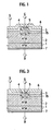
- FIG. 1 shows a first embodiment of a semiconductor device according to the present invention.
- FIG. 1 is a cross sectional diagram of two structural unit cells facing each other.
- the description is given as one example by using a semiconductor device whose substrate material is silicon carbide (SiC).
- a drain region 2 formed of an N - type silicon carbide epitaxial layer is formed on a substrate 1 formed of N + type silicon carbide in which polytype is 4H and a hetero semiconductor region 3 formed of, for example, N type polycrystalline silicon is formed so as to adjoin a main surface of the drain region 2 opposing to a junction surface with the substrate 1. That is, the junction portion between the drain region 2 and the hetero semiconductor region 3 is composed of a hetero junction formed of materials of silicon carbide and polycrystalline silicon which are different in a band gap, and an energy barrier is present on a junction interface thereof.
- a gate insulating film 4 formed of, for example, a silicon oxide film is formed so as to adjoin the junction portion between the hetero semiconductor region 3 and the drain region 2.
- a gate electrode 5 is formed on the gate insulating film 4, and a source electrode 6 is formed on the surface of the hetero semiconductor region 3 opposite to the junction surface between the hetero semiconductor region 3 and the drain region 2, and a drain electrode 7 is formed on the substrate 1 so as to be connected to the substrate 1.
- a trench 15 is formed in the drain region 2 so that a trench type structure in which the gate electrode 5 is buried is obtained.
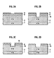
- FIGS. 2A to 2H A method of manufacturing a silicon carbide semiconductor device according to the first embodiment of the present invention shown in FIG. 1 will now be described by referring to FIGS. 2A to 2H.
- a nitride silicon film is deposited on an N type silicon carbide semiconductor body formed by epitaxialy growing the N - type drain region 2 on the N + type silicon carbide substrate 1.
- the silicon nitride film serves as an antioxidant film (mask layer) 8 and is formed by, for example, a Low Pressure-Chemical Vapor Deposition (LP-CVD) method.
- LP-CVD Low Pressure-Chemical Vapor Deposition
- a mask layer 9 having a predetermined opening is formed on the antioxidant film 8 formed of the nitride silicon film by photolithography and etching.
- the antioxidant film 8 and a surface layer portion of the drain region 2 are etched by using, for example, reactive ion etching (dry etching), and the drain region 2 is etched by a predetermined depth so that a trench 15 is formed.
- reactive ion etching dry etching
- other method may be used as long as it is an anisotropic etching.
- sacrificial oxidation is carried out by, for example, dry O 2 oxidation at 1100°C to remove the damages, thus forming a sacrificial oxide film 10.
- the nitride silicon film is formed by the LP-CVD method to be used as the antioxidant film 8
- an oxidation rate thereof is relatively close to that of the drain region 2 formed of silicon carbide. Therefore, the sacrificial oxide film 10 at the same level is formed also on the antioxidant film 8 of the nitride silicon film.
- an upper end portion of the side wall of the drain region 2 and an end portion of the antioxidant film 8 can be kept to be flush.
- the oxidation using the dry O 2 oxidation is given as one example, but any method may be used as long as the region damaged by etching in the drain region 2 can be buried into the oxide film.
- the sacrificial oxide film 10 (FIG. 2C) is removed by wet etching by use of a mixed solution of, for example, ammonium fluoride and hydrofluoric acid.
- a buried region 11 is formed by using a reflowable material such as Spin-On-Glass (SOG).
- SOG Spin-On-Glass
- the buried region 11 is formed so as to be substantially flush with the upper end portion of the trench 15 while including the trench in the antioxidant film 8.
- the trench 15 is formed so as to adjoin at least the junction interface between the drain region 2 and the antioxidant film 8
- a material for the buried region may also be formed on the antioxidant film 8, and then the buried region is formed by etchback.
- polycrystalline silicon is deposited by, for example, the LP-CVD method.
- phosphorus doping is carried out in the atmosphere of, for example, phosphoryl chloride (POCl 3 ) so that a hetero semiconductor layer 30 formed of N type polycrystalline silicon is formed.
- this polycrystalline silicon layer may be formed by laser annealing, or the like to recrystallize it after being deposited by the electronic beam evaporation method or the sputtering method, or may be formed of single crystalline silicon of hetero epitaxial growth by, for example, the molecular beam epitaxy.
- a combination of ionic implantation and activation heat treatment after the ionic implantation may be used for the doping of the polycrystalline silicon layer.
- a mask layer (not shown) having a predetermined opening is formed in a predetermined region of the hetero semiconductor layer 30 of polycrystalline silicon by the photolithography and the etching, and one portion of the hetero semiconductor layer 30 is etched by, for example, reactive ion etching (dry etching) so that a hetero semiconductor region 3 is formed.
- the buried region 11 (FIG. 2F) formed of oxide is subjected to wet etching by a mixed solution of, for example, ammonium fluoride and hydrofluoric acid.
- a gate insulating film 4 is deposited along the inner wall of the hetero semiconductor region 3 and the drain region 2. Further, a polycrystalline silicon layer to be a gate electrode 5 is deposited. After that, phosphorus is doped into the polycrystalline silicon layer to be the gate electrode 5 by solid phase diffusion using POCl 3 .
- the gate electrode 5 is formed by the photolithography, etching, or the like before a drain electrode 7 formed of, for example, titanium (Ti) and nickel (Ni) is formed on the substrate 1 corresponding to a backside surface of the semiconductor device, and a source electrode 6 (insulated from the gate electrode 5 by the insulating film) formed by sequentially depositing titanium (Ti) and nickel (Ni) is formed in the hetero semiconductor region 3 corresponding to a front surface of the semiconductor device.
- a drain electrode 7 formed of, for example, titanium (Ti) and nickel (Ni) is formed on the substrate 1 corresponding to a backside surface of the semiconductor device
- a source electrode 6 insulated from the gate electrode 5 by the insulating film formed by sequentially depositing titanium (Ti) and nickel (Ni) is formed in the hetero semiconductor region 3 corresponding to a front surface of the semiconductor device.
- the gate electrode 5 is buried in the trench is given as one example, but it may be formed so as to extend onto the hetero semiconductor region 3 through the gate insulating film 4.
- the neighboring regions are connected each other in such a manner that the source electrode 6 covers the gate electrode through the insulating film, but they do not have to be connected.
- the present embodiment has a structure where, in a method of manufacturing a semiconductor device including a semiconductor body of a first conductivity type (a substrate 1 and a drain region 2), a hetero semiconductor region 3 adjacent to one main surface of the semiconductor body and having a band gap different from that of the semiconductor body, a gate electrode 5 formed in a junction portion between the hetero semiconductor region 3 and the semiconductor body through a gate insulating film 4, a source electrode 6 connected to the hetero semiconductor region 3, and a drain electrode 7 having an ohmic connection with the semiconductor body, the method of manufacturing the semiconductor device includes at least a first process of forming a predetermined trench 15 on the main surface side of the semiconductor body by using a mask layer 9 having a predetermined opening, a second process of forming a buried region 11 so as to adjoin at least a side wall of the trench 15 and extend from the trench 15, a third process of forming a hetero semiconductor layer 30 so as to adjoin the semiconductor body and the buried region 11, and a fourth process of forming the hetero semiconductor region 3 by pattern
- the semiconductor device according to the present embodiment can be easily obtained with an earlier manufacturing technique.
- a structure in which an upper end portion of the trench 15 of the drain region 2 with etching damage removed comes to be a substantially flush with an end portion of the hetero semiconductor region 3 can be easily formed.
- the gate electrode 5 can be formed through the gate insulating film 4 so as to oppose substantially perpendicular to a junction interface between the drain region 2 and the hetero semiconductor region 3. Therefore, an electric filed effectively expands to the hetero junction interface depending on a voltage applied to the gate electrode 5 and driving force during conduction is improved.
- the upper end portion of the trench 15 in the drain region 2 can be further easily formed to be substantially flush with the end portion of the hetero semiconductor region 3.
- the hetero semiconductor region 3 may be formed by etching back the hetero semiconductor layer 30.
- the source electrode 6 can be formed on a flat surface so that reliability of the semiconductor device is improved.
- the manufacturing processes come to be easy. That is, a material which is easily etched by wet etching and has a relatively large selection ratio to the drain region 2 and the hetero semiconductor region 3 is used for the buried region 11. Therefore, the manufacturing processes come to be easy.
- a process of forming the gate insulating film 4 so as to adjoin the hetero interface between the hetero semiconductor region 3 and the semiconductor body is included. With this, it is possible to provide a hetero junction insulated gate field effect transistor with easy manufacturing processes.
- a process of sacrificial oxidation is included.
- the gate electrode 5 can be formed through the gate insulating film 4 so as to oppose substantially perpendicular to the junction interface between the drain region 2 and the hetero semiconductor region 3. Therefore, an electric field effectively expands to the hetero junction interface depending on a voltage applied to the gate electrode 5 so that driving force during conduction is improved.
- the semiconductor body is formed of silicon carbide. With this, a semiconductor with a high break down voltage can be easily obtained by using a general semiconductor material.
- the hetero semiconductor region 3 is formed of at least one of single crystalline silicon, polycrystalline silicon, and amorphous silicon. With this, a semiconductor device can be easily obtained by using a general semiconductor material.
- the antioxidant film 8 of the mask layer is formed of a material having a similar value to that of a thermal oxidation rate of silicon carbide.
- a sacrificial oxide film 10 at the same level is formed also on the antioxidant film 8 of the nitride silicon film. Therefore, the upper end portion of the side wall of the drain region 2 and the end portion of the antioxidant film 8 can retain to be substantially flush with each other.
- the source electrode 6 is grounded and a positive potential is applied to the drain electrode 7.
- the gate electrode 5 is, for example, grounded or is a negative potential, a shielding state is kept. It is because that energy barrier is formed to conduction electron on both sides of the hetero junction interface between the hetero semiconductor region 3 and the drain region 2.
- the gate electrode 5 can be formed through the gate insulating film 4 so as to oppose substantially perpendicular to the junction interface between the drain region 2 and the hetero semiconductor region 3. Therefore, the electric filed effectively expands to the hetero junction interface depending on a voltage applied to the gate electrode 5 so that high driving force can be obtained.
- the gate electrode 5 is grounded again so as to change the conducting state to the shielding state, the accumulation state of the conduction electron formed in the hetero junction interface between the hetero semiconductor region 3 and the drain region 2 is relieved, and then tunneling in the energy barrier stops. Consequently, the flow of the conduction electron from the hetero semiconductor region 3 to the drain region 2 stops. Further, the conduction electron in the drain region 2 flows to the substrate 1, and when the conduction electron is depleted, a depletion layer expands from the hetero junction portion to the drain region 2 side, resulted in the shielding state.
- reverse direction conduction (reflux operation) is possible in which, for example, the source electrode 6 is grounded and a negative potential is applied to the drain electrode 7.
- the source electrode 6 and the gate electrode 5 are grounded and a predetermined electric potential is applied to the drain electrode 7, the energy barrier for the conduction electron disappears, and the conduction electron flows from the drain region 2 side to the hetero semiconductor region 3, resulted in a reverse conduction state.
- a positive hole is not infused, and conduction is carried out only by the conduction electron. Therefore, loss of the conduction electron due to reverse recovery current is small at the time of changing the reverse conduction state to the shielding state.
- the above described gate electrode 5 is used as a control electrode without being grounded is also possible.
- a structure of FIG. 3 is different when compared with the structure of FIG. 1 in that a hetero semiconductor region 3 is flatly formed, a gate insulating film 4 is formed on a side wall of a trench 15, a gate electrode 5 is buried to be flat in the trench 15, and a source electrode 6 is flatly formed on a surface of an element.
- FIGS. 4A to 4B Next, a method of manufacturing a semiconductor device of silicon carbide having the structure shown in FIG. 3 will be described by referring to FIGS. 4A to 4B.
- FIGS. 2A to 2F showing manufacturing processes of the structure of FIG. 1 have the same structure with that of FIG. 3.
- the hetero semiconductor region 3 is processed to be flat by Chemical Mechanical Polishing (CMP), and as shown in FIG. 4A, a surface including the hetero semiconductor region 3 and a buried region 11 is flatly formed.
- CMP Chemical Mechanical Polishing
- the buried region 11 formed of oxidant is subjected to wet etching by a mixed solution of, for example, ammonium fluoride and hydrofluoric acid so as to be a state shown in FIG. 4B.
- a gate insulating film 4 is deposited along an inner wall of the hetero semiconductor region 3 and a drain region 2. Further, a polycrystal layer to be the gate electrode 5 is deposited. After that, phosphorus is doped into the polycrystalline silicon layer to be the gate electrode 5 by solid phase diffusion using POCl 3 .
- the gate electrode 5 is formed by the photolithography, etching, or the like before a drain electrode 7 formed of, for example, titanium (Ti) and nickel (Ni) is formed on a substrate 1 corresponding to a backside surface of the semiconductor device, and a source electrode 6 (insulated from the gate electrode 5 by the insulating film) formed by sequentially depositing titanium (Ti) and nickel (Ni) is formed in the hetero semiconductor region 3 corresponding to a front surface of the semiconductor device.
- a drain electrode 7 formed of, for example, titanium (Ti) and nickel (Ni) is formed on a substrate 1 corresponding to a backside surface of the semiconductor device
- a source electrode 6 insulated from the gate electrode 5 by the insulating film
- the case where the gate electrode 5 is buried in the trench is given as one example, but it may be formed through the gate insulating film 4 so as to extend onto the hetero semiconductor region 3.
- the neighboring regions are connected each other in such a manner that the source electrode 6 covers the gate electrode through the insulating film, but they do not have to be connected.
- the hetero semiconductor region 3 is formed by carrying out Chemical Mechanical Polishing (CMP) for the hetero semiconductor layer 30.
- CMP Chemical Mechanical Polishing
- FIGS. 5A to 5F another manufacturing method according to the present embodiment will be described below.
- a completed structure is the same with that of FIG. 3.
- FIGS. 2A to 2D showing the method of manufacturing the structure of FIG. 1 have the same structure with that of FIG. 1.
- an insulating film 4 is deposited along an inner wall of an antioxidant film (mask layer) 8 and a drain region 2.
- a polycrystalline silicon layer 50 to be a gate electrode 5 is deposited.
- phosphorus is doped into the polycrystalline silicon layer 50 to be the gate electrode 5 by solid phase diffusion using POCl 3 .
- the polycrystalline silicon layer 50 is etched back to be a state shown in FIG. 5B so that the gate electrode 5 is formed.
- a cap oxide film 16 is formed in an upper portion of the gate electrode 5 by thermal oxidation.
- the antioxidant film 8 formed of silicon nitride is removed by, for example, phosphoric acid solution before polycrystalline silicon is deposited by, for example, the LP-CVD method.
- phosphorus doping is carried out in the atmosphere of, for example, POCl 3 so that a hetero semiconductor layer 30 formed of an N - type polycrystalline silicon is formed.
- this polycrystalline silicon layer may be formed by laser annealing to recrystallize it after being deposited by the electronic beam evaporation method or the sputtering method, or may be formed of single crystalline silicon of the hetero epitaxial growth by, for example, the molecular beam epitaxy.
- a combination of ionic implantation and activation heat treatment after the ionic implantation may be used.
- the hetero semiconductor region 3 is processed to be flat by Chemical Mechanical Polishing, a drain electrode 7 formed of, for example, titanium (Ti) and nickel (Ni) is formed on a substrate 1 corresponding to a backside surface of the semiconductor device, and a source electrode 6 is formed by sequentially depositing titanium (Ti) and aluminum (A1) in the hetero semiconductor region 3 corresponding to a front surface of the semiconductor device.
- a drain electrode 7 formed of, for example, titanium (Ti) and nickel (Ni) is formed on a substrate 1 corresponding to a backside surface of the semiconductor device
- a source electrode 6 is formed by sequentially depositing titanium (Ti) and aluminum (A1) in the hetero semiconductor region 3 corresponding to a front surface of the semiconductor device.
- the present embodiment has a structure where, in a method of manufacturing the semiconductor device including the semiconductor body of a first conductivity type (the substrate 1 and the drain region 2), the hetero semiconductor region 3 adjacent to the one main surface of the semiconductor body and having a band gap different from that of the semiconductor body, the gate electrode 5 formed in the junction portion between the hetero semiconductor region 3 and the semiconductor body through the gate insulating film 4, the source electrode 6 connected to the hetero semiconductor region 3, and the drain electrode 7 having the ohmic connection with the semiconductor body, the method of manufacturing the semiconductor device includes at least a first process of forming the predetermined trench 15 on the main surface side of the semiconductor body by using the mask layer having a predetermined opening, a second process of forming the gate insulating film 4 so as to adjoin at least the side wall of the trench 15 , a third process of forming the gate electrode 5 adjacent to the gate insulating film 4, a fourth process of forming the hetero semiconductor layer 30 on the gate electrode 5 through the cap oxide film 16 which is an interlayer insulating film, and a
- the semiconductor device according to the present embodiment can be easily obtained with a conventional manufacturing technique.
- a structure in which an upper end portion of the trench 15 of the drain region 2 with etching damages removed comes to be substantially flush with an end portion of the hetero semiconductor region 3 can be easily formed.
- the gate electrode 5 can be formed through the gate insulating film 4 so as to oppose substantially perpendicular to the junction interface between the drain region 2 and the hetero semiconductor region 3. Therefore, an electric filed effectively expands to the hetero junction interface depending on a voltage applied to the gate electrode 5 so that driving force during conduction is improved.
- the upper end portion of the trench 15 in the drain region 2 can be further easily formed to be substantially flush with the end portion of the hetero semiconductor region 3.
- the gate insulating film 4 includes at least a thermal oxide film formed by thermal oxidation. With this, a quality gate insulating film can be easily formed so that improvement of driving force during the conducting state can be expected and high reliability can be obtained.
- a structure of FIG. 6 is different from that of FIG. 1 in that a hetero semiconductor region 3 formed of, for example, N - type polycrystalline silicon and a second hetero semiconductor region 12 formed of P - type polycrystalline silicon are formed so as to adjoin a main surface opposing to a junction surface between a drain region 2 and a substrate 1. That is, the junction portion of the drain 2, the hetero semiconductor region 3, and the second hetero semiconductor regions 12 has a hetero junction by materials having different band gap from that of SiC and polycrystal, and energy barriers are formed in the junction interface thereof.
- a gate insulating film 4 formed of, for example, a silicon oxide film is formed so as to adjoin the junction portion between the hetero semiconductor region 3 and the drain region 2.
- a gate electrode 5 is formed to be connected to the gate insulating film 4
- a source electrode 6 is connected on an opposite surface opposing to the junction surface of the drain region 2 with the hetero semiconductor region 3 and the second hetero semiconductor region 12, and a drain electrode 7 is connected on the substrate 1.
- the hetero semiconductor region 3 is formed before P - type impurity of reverse conductivity type that is, for example, a reverse conductivity type of the N - type hetero semiconductor region 3 is introduced into a predetermined portion (second hetero semiconductor regions 12) in the hetero semiconductor region 3.
- P - type impurity of reverse conductivity type that is, for example, a reverse conductivity type of the N - type hetero semiconductor region 3 is introduced into a predetermined portion (second hetero semiconductor regions 12) in the hetero semiconductor region 3.
- a width of a depletion layer extended from the junction interface of the drain region 2 comes to be different. That is, the width of the depletion layer extended from the junction interface with the second hetero semiconductor region 12 is larger than the width of the depletion layer expanded from the junction interface with the hetero semiconductor region 3. Therefore, higher performance of shielding can be obtained, that is, leakage current can be reduced. Further, when, for example, the impurity concentration of the second hetero semiconductor region 12 is provided to be higher than that of the hetero semiconductor region 3, the depletion layer generated by built-in electric field of P-N diode formed of the second hetero semiconductor region 12 and the hetero semiconductor region 3 extends to the hetero semiconductor region 3 side. Therefore, the leakage current in the hetero junction between the hetero semiconductor region 3 and the drain region can be further reduced.
- the shielding performance of the semiconductor device can be further increased when, for example, the gate electrode 5 is provided to be a negative potential, and a revere region is formed in, for example, an entire region of the hetero semiconductor region 3.
- FIG. 7 is such that an N + type conducting region 13 having higher concentration than that of a drain region 2 is formed in a predetermined portion between a gate insulating film 4 and the drain region 2 in the structure of FIG. 1.
- the description of a manufacturing method thereof will be given below as one example.
- the doping of phosphorus is carried out in the atmosphere of, for example, POCl 3 with a higher temperature, the phosphorus is introduced onto the surface of silicon carbide so that an N + type conducting region 13 is formed.
- introduction of impurity with solid phase diffusion, or a method of introducing impurity with, for example, ionic implantation may be used.
- a structure of FIG. 8 is such that, in addition to the structure of FIG. 1, an electric field relaxation region 14 is formed on a surface of a drain region 2 so as to adjoin the hetero semiconductor region 3 and space apart a predetermined distance from a portion in which a gate electrode 5 and a hetero semiconductor region 3 are opposed each other.
- an electric field relaxation region 14 is formed on a surface of a drain region 2 so as to adjoin the hetero semiconductor region 3 and space apart a predetermined distance from a portion in which a gate electrode 5 and a hetero semiconductor region 3 are opposed each other.
- the P type electric field relaxation region 14 is formed by the ionic implantation of aluminum ion or boron ion by using the mask layer having a predetermined opening as a mask. It should be noted that it may be formed by solid phase diffusion. The subsequent processes are the same with that of manufacturing the structure of FIG. 1.
- a depletion layer spreads between the electric filed relaxation region 14 and the drain region 2 depending on a drain potential. That is, the leakage current is further reduced and the shielding performance is improved since a drain potential applied to the hetero junction between the hetero semiconductor region 3 and the drain region 2 is relieved by the electric field relaxation region 14.
- a structure of FIG. 9 is a modified example of the structure of FIG. 1, and a trench 17 is formed in the drain region 2 before the antioxidant film 8 is formed in FIG. 2A. After that, the hetero semiconductor layer 30 is formed. The sequent processes are the same with that of manufacturing the structure of FIG. 1. With this structure, the leakage current in the hetero semiconductor region 3 can be further reduced than the structure of FIG. 1.
- FIGS. 6 to 9 As described above, using the basic processes of the present invention, various structures as shown in FIGS. 6 to 9 can be formed.
- a semiconductor device using silicon carbide as a substrate material is described as one example, the material for the substrate may be other semiconductor materials such as silicon, silicon germanium, gallium nitride, and diamond.
- silicon carbide whose polytype is 4H is used as one example for the description, but it may be other polytype such as 6H and 3C.
- a transistor having so-called a vertical structure in which a drain electrode 7 and a source electrode 6 are disposed to oppose each other with the drain region 2 sandwiched therebetween so that drain current flow occurs vertically is used for the description, but a transistor having so-called a horizontal structure in which, for example, a drain electrode 7 and a source electrode 6 are disposed to be flush with each other so that drain current flow occurs horizontally, may be used.
- the description is given by using polycrystal as a material used for a hetero semiconductor region 3 or a second hetero semiconductor region 12 as one example, but the material can be any material as long as it forms a hetero junction with silicon carbide. Still furthermore, as one example, the description is given by using an N - type silicon carbide as a drain region 2 and an N - type polycrystalline silicon as a hetero semiconductor region 3, but it may be any combination of N - type silicon carbide and P - type polycrystalline silicon, P - type silicon carbide and P - type polycrystalline silicon, and P - type silicon carbide and N - type polycrystalline silicon.
- a mask layer used for forming a predetermined trench on a main surface side of a semiconductor body corresponds to a mask layer 9 and an antioxidant film 8 in the
Landscapes
- Engineering & Computer Science (AREA)
- Microelectronics & Electronic Packaging (AREA)
- Power Engineering (AREA)
- Condensed Matter Physics & Semiconductors (AREA)
- Physics & Mathematics (AREA)
- Ceramic Engineering (AREA)
- General Physics & Mathematics (AREA)
- Computer Hardware Design (AREA)
- Chemical & Material Sciences (AREA)
- Manufacturing & Machinery (AREA)
- Crystallography & Structural Chemistry (AREA)
- Insulated Gate Type Field-Effect Transistor (AREA)
- Electrodes Of Semiconductors (AREA)
Abstract
Description
- The present invention relates to a method of manufacturing a semiconductor device.
- As the related art which is the background of the present invention,
Japanese Patent Application Publication No. 2003-318398 - The semiconductor device of the related art having the structure as described above functions as a switching device by controlling an electric potential of the gate electrode in a state where the source electrode is grounded and a predetermined positive electric potential is applied to the drain electrode. That is, in the state where the gate electrode is grounded, reverse bias is applied to the hetero junction formed of the N- type polycrystalline silicon region, the N+ type polycrystalline silicon region and the epitaxial region so that no current flows between the drain electrode and the source electrode. However, in the state where the predetermined positive voltage is applied to the gate electrode, gate electric filed acts on a hetero junction interface between the N+ type polycrystalline silicon region and the epitaxial region, and an energy barrier formed by the hetero junction surface on a gate oxide film interface is made to be thin. Therefore, current flows between the drain electrode and the source electrode. In this related art, since the hetero junction portion is used as a control channel for cutting-off and flowing of the current, the device functions with a channel length having a thickness equal to that of the hetero barrier. Therefore, a conduction characteristic of low resistance can be obtained.
- However, in the related art, driving force is lowered because damages are caused on an etching surface of the silicon carbide epitaxial region when a physical etching such as a dry etching is used at the time of patterning the polycrystalline silicon region formed on the silicon carbide epitaxial region to form a channel interface between the polycrystalline silicon region and the silicon carbide epitaxial region.
- The present invention has been made to solve the above problems of the related art. Accordingly, it is an object of the present invention to provide a method of manufacturing a semiconductor device capable of suppressing decrease of the driving force.
- To achieve the above objective, in the method of manufacturing a semiconductor device including a hetero semiconductor region adjacent to one main surface of a semiconductor body of a first conductivity type, which has a band gap different from that of the semiconductor body; a gate electrode formed in a junction portion between the hetero semiconductor region and the semiconductor body through a gate insulating film, a source electrode connected to the hetero semiconductor region, and a drain electrode having an ohmic connection with the semiconductor body, the method of manufacturing the semiconductor device includes the processes of forming a predetermined trench on the main surface side of the semiconductor body by using a mask layer having a predetermined opening, forming a buried region adjacent to at least a side wall of the trench so as to be extended from the trench, forming a hetero semiconductor layer so as to adjoin the semiconductor body and the buried region, and forming the hetero semiconductor region by patterning the hetero semiconductor layer.
-
- FIG. 1 is a cross sectional diagram showing a semiconductor device according to a first embodiment of the present invention;
- FIGS. 2A to 2H are cross sectional diagrams showing a method of manufacturing a silicon carbide semiconductor device according to the first embodiment of the present invention shown in FIG. 1;
- FIG. 3 is a cross sectional diagram showing a structure that is different from FIG. 1 in that a
hetero semiconductor region 3 is flatly formed; - FIGS. 4A to 4B are cross sectional diagrams showing a method of manufacturing a semiconductor device shown in FIG. 3;
- FIGS. 5A to 5F are cross sectional diagrams showing another method of manufacturing semiconductor device show in FIG. 3;
- FIG. 6 is a cross sectional diagram showing a structure that is different from FIG. 1 in that a hetero semiconductor region 3 (N-type polycrystalline silicon) and a second hetero semiconductor region 12 (P-type polycrystalline silicon) are formed;
- FIG. 7 is a cross sectional diagram showing a structure that is different from FIG. 1 in that N+
type conducting region 13 having higher concentration than that of adrain region 2 is formed; - FIG. 8 is a cross sectional diagram showing a structure, in addition to the structure of FIG. 1, an electric
field relaxation region 14 is formed on a surface of adrain region 2; and - FIG. 9 is a cross sectional diagram showing a modified example of the structure of FIG. 1.
- Detailed description of preferred embodiments of the present invention will be given below by referring to the accompanying drawings. It should be noted that the same reference numerals are used in the following drawings among the components having same function, and the same description is not repeated.
- FIG. 1 shows a first embodiment of a semiconductor device according to the present invention. FIG. 1 is a cross sectional diagram of two structural unit cells facing each other. In the present embodiment, the description is given as one example by using a semiconductor device whose substrate material is silicon carbide (SiC).
- For example, a
drain region 2 formed of an N- type silicon carbide epitaxial layer is formed on asubstrate 1 formed of N+ type silicon carbide in which polytype is 4H and ahetero semiconductor region 3 formed of, for example, N type polycrystalline silicon is formed so as to adjoin a main surface of thedrain region 2 opposing to a junction surface with thesubstrate 1. That is, the junction portion between thedrain region 2 and thehetero semiconductor region 3 is composed of a hetero junction formed of materials of silicon carbide and polycrystalline silicon which are different in a band gap, and an energy barrier is present on a junction interface thereof. Agate insulating film 4 formed of, for example, a silicon oxide film is formed so as to adjoin the junction portion between thehetero semiconductor region 3 and thedrain region 2. In addition, agate electrode 5 is formed on thegate insulating film 4, and asource electrode 6 is formed on the surface of thehetero semiconductor region 3 opposite to the junction surface between thehetero semiconductor region 3 and thedrain region 2, and adrain electrode 7 is formed on thesubstrate 1 so as to be connected to thesubstrate 1. In the present embodiment, as shown in FIG. 1, atrench 15 is formed in thedrain region 2 so that a trench type structure in which thegate electrode 5 is buried is obtained. - A method of manufacturing a silicon carbide semiconductor device according to the first embodiment of the present invention shown in FIG. 1 will now be described by referring to FIGS. 2A to 2H.
- First, as shown in FIG. 2A, a nitride silicon film is deposited on an N type silicon carbide semiconductor body formed by epitaxialy growing the N-
type drain region 2 on the N+ typesilicon carbide substrate 1. The silicon nitride film serves as an antioxidant film (mask layer) 8 and is formed by, for example, a Low Pressure-Chemical Vapor Deposition (LP-CVD) method. Further, amask layer 9 having a predetermined opening is formed on theantioxidant film 8 formed of the nitride silicon film by photolithography and etching. - As shown in FIG. 2B, by using the
mask layer 9 as a mask, theantioxidant film 8 and a surface layer portion of thedrain region 2 are etched by using, for example, reactive ion etching (dry etching), and thedrain region 2 is etched by a predetermined depth so that atrench 15 is formed. It should be noted that as a method of etching theantioxidant film 8 formed of the nitride silicon film and thedrain region 2, other method may be used as long as it is an anisotropic etching. - As shown in FIG. 2C, since etching damages are caused in the etched
drain region 2 by dry etching, sacrificial oxidation is carried out by, for example, dry O2 oxidation at 1100°C to remove the damages, thus forming asacrificial oxide film 10. At this time, in the present embodiment, since the nitride silicon film is formed by the LP-CVD method to be used as theantioxidant film 8, an oxidation rate thereof is relatively close to that of thedrain region 2 formed of silicon carbide. Therefore, thesacrificial oxide film 10 at the same level is formed also on theantioxidant film 8 of the nitride silicon film. Thus, an upper end portion of the side wall of thedrain region 2 and an end portion of theantioxidant film 8 can be kept to be flush. It should be noted that as a method of forming thesacrificial oxide film 10, the oxidation using the dry O2 oxidation is given as one example, but any method may be used as long as the region damaged by etching in thedrain region 2 can be buried into the oxide film. - As shown in FIG. 2D, the sacrificial oxide film 10 (FIG. 2C) is removed by wet etching by use of a mixed solution of, for example, ammonium fluoride and hydrofluoric acid.
- As shown in FIG. 2E, a buried
region 11 is formed by using a reflowable material such as Spin-On-Glass (SOG). In the present embodiment, there is shown a case where the buriedregion 11 is formed so as to be substantially flush with the upper end portion of thetrench 15 while including the trench in theantioxidant film 8. However, as long as thetrench 15 is formed so as to adjoin at least the junction interface between thedrain region 2 and theantioxidant film 8, there is no problem in that it is not completely buried, or extended from the trench to the outside. In addition, at the time of forming the buriedregion 11, a material for the buried region may also be formed on theantioxidant film 8, and then the buried region is formed by etchback. - As shown in FIG. 2F, after the
antioxidant film 8 formed of nitride silicon is removed by, for example, a phosphate solution, polycrystalline silicon is deposited by, for example, the LP-CVD method. After that, phosphorus doping is carried out in the atmosphere of, for example, phosphoryl chloride (POCl3) so that ahetero semiconductor layer 30 formed of N type polycrystalline silicon is formed. It should be noted that this polycrystalline silicon layer may be formed by laser annealing, or the like to recrystallize it after being deposited by the electronic beam evaporation method or the sputtering method, or may be formed of single crystalline silicon of hetero epitaxial growth by, for example, the molecular beam epitaxy. In addition, for the doping of the polycrystalline silicon layer, a combination of ionic implantation and activation heat treatment after the ionic implantation may be used. - As shown in FIG. 2G, a mask layer (not shown) having a predetermined opening is formed in a predetermined region of the
hetero semiconductor layer 30 of polycrystalline silicon by the photolithography and the etching, and one portion of thehetero semiconductor layer 30 is etched by, for example, reactive ion etching (dry etching) so that ahetero semiconductor region 3 is formed. Then, for example, the buried region 11 (FIG. 2F) formed of oxide is subjected to wet etching by a mixed solution of, for example, ammonium fluoride and hydrofluoric acid. - Lastly, as shown in FIG. 2H, a
gate insulating film 4 is deposited along the inner wall of thehetero semiconductor region 3 and thedrain region 2. Further, a polycrystalline silicon layer to be agate electrode 5 is deposited. After that, phosphorus is doped into the polycrystalline silicon layer to be thegate electrode 5 by solid phase diffusion using POCl3. After that, thegate electrode 5 is formed by the photolithography, etching, or the like before adrain electrode 7 formed of, for example, titanium (Ti) and nickel (Ni) is formed on thesubstrate 1 corresponding to a backside surface of the semiconductor device, and a source electrode 6 (insulated from thegate electrode 5 by the insulating film) formed by sequentially depositing titanium (Ti) and nickel (Ni) is formed in thehetero semiconductor region 3 corresponding to a front surface of the semiconductor device. Thus, the silicon carbide semiconductor device according to the first embodiment of the present invention shown in FIG. 1 is completed. It should be noted that, in the present embodiment, the case where thegate electrode 5 is buried in the trench is given as one example, but it may be formed so as to extend onto thehetero semiconductor region 3 through thegate insulating film 4. In addition, there is given one example that the neighboring regions are connected each other in such a manner that thesource electrode 6 covers the gate electrode through the insulating film, but they do not have to be connected. - As described above, the present embodiment has a structure where, in a method of manufacturing a semiconductor device including a semiconductor body of a first conductivity type (a
substrate 1 and a drain region 2), ahetero semiconductor region 3 adjacent to one main surface of the semiconductor body and having a band gap different from that of the semiconductor body, agate electrode 5 formed in a junction portion between thehetero semiconductor region 3 and the semiconductor body through agate insulating film 4, asource electrode 6 connected to thehetero semiconductor region 3, and adrain electrode 7 having an ohmic connection with the semiconductor body, the method of manufacturing the semiconductor device includes at least a first process of forming apredetermined trench 15 on the main surface side of the semiconductor body by using amask layer 9 having a predetermined opening, a second process of forming a buriedregion 11 so as to adjoin at least a side wall of thetrench 15 and extend from thetrench 15, a third process of forming ahetero semiconductor layer 30 so as to adjoin the semiconductor body and the buriedregion 11, and a fourth process of forming thehetero semiconductor region 3 by patterning thehetero semiconductor layer 30. - With this structure, the semiconductor device according to the present embodiment can be easily obtained with an earlier manufacturing technique. In addition, with this manufacturing method, a structure in which an upper end portion of the
trench 15 of thedrain region 2 with etching damage removed comes to be a substantially flush with an end portion of thehetero semiconductor region 3 can be easily formed. With this, thegate electrode 5 can be formed through thegate insulating film 4 so as to oppose substantially perpendicular to a junction interface between thedrain region 2 and thehetero semiconductor region 3. Therefore, an electric filed effectively expands to the hetero junction interface depending on a voltage applied to thegate electrode 5 and driving force during conduction is improved. In addition, by using a nitride silicon film as anantioxidant film 8, in the present embodiment in which thedrain region 2 is formed of silicon carbide, the upper end portion of thetrench 15 in thedrain region 2 can be further easily formed to be substantially flush with the end portion of thehetero semiconductor region 3. - In addition, in the fourth process, the
hetero semiconductor region 3 may be formed by etching back thehetero semiconductor layer 30. With this, thesource electrode 6 can be formed on a flat surface so that reliability of the semiconductor device is improved. - As the buried
region 11 is formed of a material which is removable after the third process, the manufacturing processes come to be easy. That is, a material which is easily etched by wet etching and has a relatively large selection ratio to thedrain region 2 and thehetero semiconductor region 3 is used for the buriedregion 11. Therefore, the manufacturing processes come to be easy. - After the fourth process, a process of forming the
gate insulating film 4 so as to adjoin the hetero interface between thehetero semiconductor region 3 and the semiconductor body is included. With this, it is possible to provide a hetero junction insulated gate field effect transistor with easy manufacturing processes. - Between the first process and the second process, a process of sacrificial oxidation is included. With this, a structure in which the upper end portion of the
trench 15 in thedrain region 2 comes to be substantially flush with the end portion of thehetero semiconductor region 3 while etching damages are removed can be easily formed. Thus, thegate electrode 5 can be formed through thegate insulating film 4 so as to oppose substantially perpendicular to the junction interface between thedrain region 2 and thehetero semiconductor region 3. Therefore, an electric field effectively expands to the hetero junction interface depending on a voltage applied to thegate electrode 5 so that driving force during conduction is improved. - Meanwhile, the semiconductor body is formed of silicon carbide. With this, a semiconductor with a high break down voltage can be easily obtained by using a general semiconductor material.
- Furthermore, the
hetero semiconductor region 3 is formed of at least one of single crystalline silicon, polycrystalline silicon, and amorphous silicon. With this, a semiconductor device can be easily obtained by using a general semiconductor material. - In addition, the
antioxidant film 8 of the mask layer is formed of a material having a similar value to that of a thermal oxidation rate of silicon carbide. With this, asacrificial oxide film 10 at the same level is formed also on theantioxidant film 8 of the nitride silicon film. Therefore, the upper end portion of the side wall of thedrain region 2 and the end portion of theantioxidant film 8 can retain to be substantially flush with each other. - Next, operations will be described. In the present embodiment, for example, the
source electrode 6 is grounded and a positive potential is applied to thedrain electrode 7. - First, when the
gate electrode 5 is, for example, grounded or is a negative potential, a shielding state is kept. It is because that energy barrier is formed to conduction electron on both sides of the hetero junction interface between thehetero semiconductor region 3 and thedrain region 2. - Next, when a positive potential is applied to the
gate electrode 5 so that the shielding state is changed to a conduction state, a gate electric field reaches the hetero junction interface in which thehetero semiconductor region 3 and thedrain region 2 are adjacent through thegate insulating film 4. Therefore, an accumulation layer of conduction electron is formed in thehetero semiconductor region 3 and thedrain region 2 that are in the vicinity of thegate electrode 5. That is, a potential on the side of thehetero semiconductor region 3 in the junction interface between thehetero semiconductor region 3 and drainregion 2 that are in the vicinity of thegate electrode 5 is depressed, and the energy barrier on thedrain region 2 side comes to be precipitous. Therefore, it is possible that the conduction electron conducts through the energy barriers. In this time, by using this manufacturing method, a structure in which the upper end portion of thetrench 15 in thedrain region 2 with the etching damages removed comes to be substantially flush with the end portion of thehetero semiconductor region 3 can be easily formed. With this, thegate electrode 5 can be formed through thegate insulating film 4 so as to oppose substantially perpendicular to the junction interface between thedrain region 2 and thehetero semiconductor region 3. Therefore, the electric filed effectively expands to the hetero junction interface depending on a voltage applied to thegate electrode 5 so that high driving force can be obtained. - Next, when the
gate electrode 5 is grounded again so as to change the conducting state to the shielding state, the accumulation state of the conduction electron formed in the hetero junction interface between thehetero semiconductor region 3 and thedrain region 2 is relieved, and then tunneling in the energy barrier stops. Consequently, the flow of the conduction electron from thehetero semiconductor region 3 to thedrain region 2 stops. Further, the conduction electron in thedrain region 2 flows to thesubstrate 1, and when the conduction electron is depleted, a depletion layer expands from the hetero junction portion to thedrain region 2 side, resulted in the shielding state. - In addition, in this structure, similar to the structure of earlier technique, reverse direction conduction (reflux operation) is possible in which, for example, the
source electrode 6 is grounded and a negative potential is applied to thedrain electrode 7. - For example, when the
source electrode 6 and thegate electrode 5 are grounded and a predetermined electric potential is applied to thedrain electrode 7, the energy barrier for the conduction electron disappears, and the conduction electron flows from thedrain region 2 side to thehetero semiconductor region 3, resulted in a reverse conduction state. In this time, a positive hole is not infused, and conduction is carried out only by the conduction electron. Therefore, loss of the conduction electron due to reverse recovery current is small at the time of changing the reverse conduction state to the shielding state. It should be noted that a case where the above describedgate electrode 5 is used as a control electrode without being grounded is also possible. - A structure of FIG. 3 is different when compared with the structure of FIG. 1 in that a
hetero semiconductor region 3 is flatly formed, agate insulating film 4 is formed on a side wall of atrench 15, agate electrode 5 is buried to be flat in thetrench 15, and asource electrode 6 is flatly formed on a surface of an element. - Next, a method of manufacturing a semiconductor device of silicon carbide having the structure shown in FIG. 3 will be described by referring to FIGS. 4A to 4B.
- First, FIGS. 2A to 2F showing manufacturing processes of the structure of FIG. 1 have the same structure with that of FIG. 3. In the structure shown in FIG. 2F, the
hetero semiconductor region 3 is processed to be flat by Chemical Mechanical Polishing (CMP), and as shown in FIG. 4A, a surface including thehetero semiconductor region 3 and a buriedregion 11 is flatly formed. - Next, for example, the buried
region 11 formed of oxidant is subjected to wet etching by a mixed solution of, for example, ammonium fluoride and hydrofluoric acid so as to be a state shown in FIG. 4B. - Lastly, as shown in FIG. 3, similar to the structure of FIG. 1, a
gate insulating film 4 is deposited along an inner wall of thehetero semiconductor region 3 and adrain region 2. Further, a polycrystal layer to be thegate electrode 5 is deposited. After that, phosphorus is doped into the polycrystalline silicon layer to be thegate electrode 5 by solid phase diffusion using POCl3. Consequently, thegate electrode 5 is formed by the photolithography, etching, or the like before adrain electrode 7 formed of, for example, titanium (Ti) and nickel (Ni) is formed on asubstrate 1 corresponding to a backside surface of the semiconductor device, and a source electrode 6 (insulated from thegate electrode 5 by the insulating film) formed by sequentially depositing titanium (Ti) and nickel (Ni) is formed in thehetero semiconductor region 3 corresponding to a front surface of the semiconductor device. Thus, the silicon carbide semiconductor device according to the structure of the present invention shown in FIG. 3 is completed. It should be noted that, also in the present embodiment, similar to FIG. 1, the case where thegate electrode 5 is buried in the trench is given as one example, but it may be formed through thegate insulating film 4 so as to extend onto thehetero semiconductor region 3. In addition, there is given one example that the neighboring regions are connected each other in such a manner that thesource electrode 6 covers the gate electrode through the insulating film, but they do not have to be connected. - In this manner, in the fourth process of forming the
hetero semiconductor region 3 by patterning the hetero semiconductor layer 30 (see, FIG. 2F), thehetero semiconductor region 3 is formed by carrying out Chemical Mechanical Polishing (CMP) for thehetero semiconductor layer 30. With this, in the manufacturing processes of the structure of FIG. 1, as shown in FIG. 2G, the processes can be simplified since it is not needed to form a mask layer (not shown) having a predetermined opening in a predetermined region on thehetero semiconductor layer 30 by photolithography and etching. In addition, the surface of the element can be flat, accordingly problems regarding reliability such as disconnection can be suppressed. - Next, referring now to FIGS. 5A to 5F, another manufacturing method according to the present embodiment will be described below. A completed structure is the same with that of FIG. 3.
- First, FIGS. 2A to 2D showing the method of manufacturing the structure of FIG. 1 have the same structure with that of FIG. 1. In the structure shown in FIG. 2D, as shown in FIG. 5A, an insulating
film 4 is deposited along an inner wall of an antioxidant film (mask layer) 8 and adrain region 2. Further, apolycrystalline silicon layer 50 to be agate electrode 5 is deposited. After that, phosphorus is doped into thepolycrystalline silicon layer 50 to be thegate electrode 5 by solid phase diffusion using POCl3. - Next, the
polycrystalline silicon layer 50 is etched back to be a state shown in FIG. 5B so that thegate electrode 5 is formed. - As shown in FIG. 5C, a
cap oxide film 16 is formed in an upper portion of thegate electrode 5 by thermal oxidation. - As shown in FIG. 5D, upper portions of the
gate insulating film 4 and thecap oxide film 16 on theantioxidant film 8 are removed by dry etching. - As shown in FIG. 5E, the
antioxidant film 8 formed of silicon nitride is removed by, for example, phosphoric acid solution before polycrystalline silicon is deposited by, for example, the LP-CVD method. After that, phosphorus doping is carried out in the atmosphere of, for example, POCl3 so that ahetero semiconductor layer 30 formed of an N-type polycrystalline silicon is formed. It should be noted that this polycrystalline silicon layer may be formed by laser annealing to recrystallize it after being deposited by the electronic beam evaporation method or the sputtering method, or may be formed of single crystalline silicon of the hetero epitaxial growth by, for example, the molecular beam epitaxy. In addition, for the doping of the polycrystalline silicon layer, a combination of ionic implantation and activation heat treatment after the ionic implantation may be used. - Lastly, similar to the structure of FIG. 4, as shown in FIG. 5F, the
hetero semiconductor region 3 is processed to be flat by Chemical Mechanical Polishing, adrain electrode 7 formed of, for example, titanium (Ti) and nickel (Ni) is formed on asubstrate 1 corresponding to a backside surface of the semiconductor device, and asource electrode 6 is formed by sequentially depositing titanium (Ti) and aluminum (A1) in thehetero semiconductor region 3 corresponding to a front surface of the semiconductor device. Thus, the silicon carbide semiconductor device according to the structure of the present invention shown in FIG. 3 is completed. - As described above, the present embodiment has a structure where, in a method of manufacturing the semiconductor device including the semiconductor body of a first conductivity type (the
substrate 1 and the drain region 2), thehetero semiconductor region 3 adjacent to the one main surface of the semiconductor body and having a band gap different from that of the semiconductor body, thegate electrode 5 formed in the junction portion between thehetero semiconductor region 3 and the semiconductor body through thegate insulating film 4, thesource electrode 6 connected to thehetero semiconductor region 3, and thedrain electrode 7 having the ohmic connection with the semiconductor body, the method of manufacturing the semiconductor device includes at least a first process of forming thepredetermined trench 15 on the main surface side of the semiconductor body by using the mask layer having a predetermined opening, a second process of forming thegate insulating film 4 so as to adjoin at least the side wall of thetrench 15 , a third process of forming thegate electrode 5 adjacent to thegate insulating film 4, a fourth process of forming thehetero semiconductor layer 30 on thegate electrode 5 through thecap oxide film 16 which is an interlayer insulating film, and a fifth process of forming thehetero semiconductor region 3 by patterning thehetero semiconductor layer 30. - With this structure, the semiconductor device according to the present embodiment can be easily obtained with a conventional manufacturing technique. In addition, with this manufacturing method, a structure in which an upper end portion of the
trench 15 of thedrain region 2 with etching damages removed comes to be substantially flush with an end portion of thehetero semiconductor region 3 can be easily formed. With this, thegate electrode 5 can be formed through thegate insulating film 4 so as to oppose substantially perpendicular to the junction interface between thedrain region 2 and thehetero semiconductor region 3. Therefore, an electric filed effectively expands to the hetero junction interface depending on a voltage applied to thegate electrode 5 so that driving force during conduction is improved. In addition, by using a silicon nitride film as theantioxidant film 8, in the present embodiment in which thedrain region 2 is formed of silicon carbide, the upper end portion of thetrench 15 in thedrain region 2 can be further easily formed to be substantially flush with the end portion of thehetero semiconductor region 3. - In addition, the
gate insulating film 4 includes at least a thermal oxide film formed by thermal oxidation. With this, a quality gate insulating film can be easily formed so that improvement of driving force during the conducting state can be expected and high reliability can be obtained. - It should be noted that the present invention has been described by using the structures shown in FIGS. 1 and 3 as one example, but it can be applied to, for example, the structures shown in FIGS. 6 to 9.
- A structure of FIG. 6 is different from that of FIG. 1 in that a
hetero semiconductor region 3 formed of, for example, N-type polycrystalline silicon and a second hetero semiconductor region 12 formed of P-type polycrystalline silicon are formed so as to adjoin a main surface opposing to a junction surface between adrain region 2 and asubstrate 1. That is, the junction portion of thedrain 2, thehetero semiconductor region 3, and the second hetero semiconductor regions 12 has a hetero junction by materials having different band gap from that of SiC and polycrystal, and energy barriers are formed in the junction interface thereof. Agate insulating film 4 formed of, for example, a silicon oxide film is formed so as to adjoin the junction portion between thehetero semiconductor region 3 and thedrain region 2. In addition, agate electrode 5 is formed to be connected to thegate insulating film 4, asource electrode 6 is connected on an opposite surface opposing to the junction surface of thedrain region 2 with thehetero semiconductor region 3 and the second hetero semiconductor region 12, and adrain electrode 7 is connected on thesubstrate 1. - In a method of manufacturing the structure of FIG. 6, the
hetero semiconductor region 3 is formed before P-type impurity of reverse conductivity type that is, for example, a reverse conductivity type of the N-typehetero semiconductor region 3 is introduced into a predetermined portion (second hetero semiconductor regions 12) in thehetero semiconductor region 3. Thus, a conductivity type and impurity concentration of the hetero semiconductor region can be freely designed. - Next, operations of this structure will be described. In essence, the structure is similar to that of FIG. 1, but with such a structure, shielding performance will be further improved. It is because that an energy barrier for conduction electron is formed in both sides of the junction interface between the
hetero semiconductor region 3 as well as the second hetero semiconductor region 12, and thedrain region 2. In this time, both of thehetero semiconductor region 3 and the second hetero semiconductor region 12 are formed of a silicon material. Therefore, an energy barrier difference Δ Ec of each of them from thedrain region 2 formed of silicon carbide comes to be substantially equal. However, the N-typehetero semiconductor region 3 and the P-type second hetero semiconductor region 12 have a difference in Fermi energy shown by energy from a conduction band to Fermi level. Therefore, a width of a depletion layer extended from the junction interface of thedrain region 2 comes to be different. That is, the width of the depletion layer extended from the junction interface with the second hetero semiconductor region 12 is larger than the width of the depletion layer expanded from the junction interface with thehetero semiconductor region 3. Therefore, higher performance of shielding can be obtained, that is, leakage current can be reduced. Further, when, for example, the impurity concentration of the second hetero semiconductor region 12 is provided to be higher than that of thehetero semiconductor region 3, the depletion layer generated by built-in electric field of P-N diode formed of the second hetero semiconductor region 12 and thehetero semiconductor region 3 extends to thehetero semiconductor region 3 side. Therefore, the leakage current in the hetero junction between thehetero semiconductor region 3 and the drain region can be further reduced. - Further, in this structure, if the
hetero semiconductor region 3 is designed to have a width with which the gate electric field reaches from thegate electrode 5, the shielding performance of the semiconductor device can be further increased when, for example, thegate electrode 5 is provided to be a negative potential, and a revere region is formed in, for example, an entire region of thehetero semiconductor region 3. - FIG. 7 is such that an N+
type conducting region 13 having higher concentration than that of adrain region 2 is formed in a predetermined portion between agate insulating film 4 and thedrain region 2 in the structure of FIG. 1. The description of a manufacturing method thereof will be given below as one example. - For example, in the state shown in FIG. 2D, the doping of phosphorus is carried out in the atmosphere of, for example, POCl3 with a higher temperature, the phosphorus is introduced onto the surface of silicon carbide so that an N+
type conducting region 13 is formed. It should be noted that introduction of impurity with solid phase diffusion, or a method of introducing impurity with, for example, ionic implantation may be used. - With this structure, in a conducting state, an energy barrier of a hetero junction between the
hetero semiconductor region 3 and the conductingregion 13 are relieved, and majority carrier comes to easily flow from thehetero semiconductor region 3 to thedrain region 2 through the conductingregion 13. In addition, a higher conducting characteristic can be obtained and on resistance can be further reduced. - A structure of FIG. 8 is such that, in addition to the structure of FIG. 1, an electric
field relaxation region 14 is formed on a surface of adrain region 2 so as to adjoin thehetero semiconductor region 3 and space apart a predetermined distance from a portion in which agate electrode 5 and ahetero semiconductor region 3 are opposed each other. The description will be given below as one example. - In FIG. 2A having the structure of FIG. 1, for example, before the
hetero semiconductor layer 30 is formed, the P type electricfield relaxation region 14 is formed by the ionic implantation of aluminum ion or boron ion by using the mask layer having a predetermined opening as a mask. It should be noted that it may be formed by solid phase diffusion. The subsequent processes are the same with that of manufacturing the structure of FIG. 1. - With this structure, in a conducting state, the energy barrier of the hetero junction between the
hetero semiconductor region 3 and thedrain region 2 is relieved, and a higher conducting characteristic can be obtained. That is, on resistance further comes to be small, accordingly the conducting performance is improved. - In addition, in a shielding state, a depletion layer spreads between the electric filed
relaxation region 14 and thedrain region 2 depending on a drain potential. That is, the leakage current is further reduced and the shielding performance is improved since a drain potential applied to the hetero junction between thehetero semiconductor region 3 and thedrain region 2 is relieved by the electricfield relaxation region 14. - A structure of FIG. 9 is a modified example of the structure of FIG. 1, and a
trench 17 is formed in thedrain region 2 before theantioxidant film 8 is formed in FIG. 2A. After that, thehetero semiconductor layer 30 is formed. The sequent processes are the same with that of manufacturing the structure of FIG. 1. With this structure, the leakage current in thehetero semiconductor region 3 can be further reduced than the structure of FIG. 1. - As described above, using the basic processes of the present invention, various structures as shown in FIGS. 6 to 9 can be formed.
- As all the structures in the preferred embodiments are described so far taking, a semiconductor device using silicon carbide as a substrate material is described as one example, the material for the substrate may be other semiconductor materials such as silicon, silicon germanium, gallium nitride, and diamond. In addition, in all the structures, silicon carbide whose polytype is 4H is used as one example for the description, but it may be other polytype such as 6H and 3C. Moreover, in all the structures, a transistor having so-called a vertical structure in which a
drain electrode 7 and asource electrode 6 are disposed to oppose each other with thedrain region 2 sandwiched therebetween so that drain current flow occurs vertically, is used for the description, but a transistor having so-called a horizontal structure in which, for example, adrain electrode 7 and asource electrode 6 are disposed to be flush with each other so that drain current flow occurs horizontally, may be used. - Furthermore, the description is given by using polycrystal as a material used for a
hetero semiconductor region 3 or a second hetero semiconductor region 12 as one example, but the material can be any material as long as it forms a hetero junction with silicon carbide. Still furthermore, as one example, the description is given by using an N-type silicon carbide as adrain region 2 and an N-type polycrystalline silicon as ahetero semiconductor region 3, but it may be any combination of N-type silicon carbide and P-type polycrystalline silicon, P-type silicon carbide and P-type polycrystalline silicon, and P-type silicon carbide and N-type polycrystalline silicon. - It is obvious that modifications may be made as long as it does not depart from the major point and the scope of the present invention.
- It should be noted that a mask layer used for forming a predetermined trench on a main surface side of a semiconductor body according to claims of the present invention corresponds to a
mask layer 9 and anantioxidant film 8 in the - Although the invention has been described above by reference to certain embodiments of the invention, the invention is not limited to the embodiments described above. Modifications and variations of the embodiments described above will occur to those skilled in the art, in light of the teachings. The scope of the invention is defined with reference to the following claims.
Claims (11)
- A method of manufacturing a semiconductor device, which includes a semiconductor body(2) of a first conductivity type; a hetero semiconductor region(3) adjacent to one main surface of the semiconductor body(2) and having a band gap different from that of the semiconductor body(2); a gate electrode(5) formed in a junction portion between the hetero semiconductor region(3) and the semiconductor body(2) through a gate insulating film(4); a source electrode(6) connected to the hetero semiconductor region; and a drain electrode(7) ohmic-connected to the semiconductor body(1), the method comprises:a first process of forming a predetermined trench(15) by using a mask layer(8) having a predetermined opening on one main surface side of the semiconductor body(2);a second process of forming a buried region(11) adjacent to at least a side wall of the trench(15) and so as to extend from the trench(15);a third process of forming a hetero semiconductor layer(30) so as to adjoin the semiconductor body(2) and the buried region(11); anda fourth process of forming the hetero semiconductor region(3) by patterning the hetero semiconductor layer(30).
- The method of manufacturing the semiconductor device according to claim 1, wherein the hetero semiconductor region(3) is formed by etching back the hetero semiconductor layer(30) in the fourth process.
- The method of manufacturing the semiconductor device according to claim 1, wherein the hetero semiconductor region(3) is formed by carrying out Chemical Mechanical Polishing for the hetero semiconductor layer(30).
- The method of manufacturing the semiconductor device according to any one of claims 1 to 3, wherein the buried region(11) is formed of a material which is removable after the third process.
- The method of manufacturing the semiconductor device according to any one of claims 1 to 4, wherein a process of forming the gate insulating film (4) so as to adjoin a hetero junction interface between the hetero semiconductor region(3) and the semiconductor body(2) is included after the fourth process.
- A method of manufacturing a semiconductor device, which includes a semiconductor body(2) of a first conductivity type; a hetero semiconductor region(3) adjacent to one main surface of the semiconductor body(2) and having a band gap different from that of the semiconductor body(2); a gate electrode(5) formed in a junction portion between the hetero semiconductor region(3) and the semiconductor body(2) through a gate insulating film(4); a source electrode(6) connected to the hetero semiconductor region(3); and a drain electrode(7) ohmic-connected to the semiconductor body(1), the method comprises:a first process of forming a predetermined trench(15) by using a mask layer(8) having a predetermined opening on one main surface side of the semiconductor body(2);a second process of forming the gate insulating film(4) adjacent to at least a side wall of the trench(15);a third process of forming the gate electrode(5) adjacent to the gate insulating film(4);a fourth process of forming a hetero semiconductor layer(30) on the semiconductor body(2) and the gate electrode(5) through an interlayer insulating film(16); anda fifth process of forming the hetero semiconductor region(3) by patterning the hetero semiconductor layer(30).
- The method of manufacturing the semiconductor device according to claim 6, wherein the gate insulating film(4) includes at least a thermal oxide film formed by thermal oxidation.
- The method of manufacturing the semiconductor device according to any one of claims 1 to 7, wherein a process of sacrificial oxidation is included between the first process and the second process.
- The method of manufacturing the semiconductor device according to any one of claims 1 to 8, wherein the semiconductor body(2) is formed of silicon carbide.
- The method of manufacturing the semiconductor device according to any one of claims 1 to 9, wherein the hetero semiconductor region(3) is formed of at least one of single crystalline silicon, polycrystalline silicon, and amorphous silicon.
- The method of manufacturing the semiconductor device according to claim 9 or 10, wherein the mask layer(8) is formed of a material having an approximate value to a thermal oxidation rate of silicon carbide.
Priority Applications (1)
| Application Number | Priority Date | Filing Date | Title |
|---|---|---|---|
| EP06005196.8A EP1835543B1 (en) | 2006-03-14 | 2006-03-14 | Method for manufacturing a semiconductor device |
Applications Claiming Priority (1)
| Application Number | Priority Date | Filing Date | Title |
|---|---|---|---|
| EP06005196.8A EP1835543B1 (en) | 2006-03-14 | 2006-03-14 | Method for manufacturing a semiconductor device |
Publications (2)
| Publication Number | Publication Date |
|---|---|
| EP1835543A1 true EP1835543A1 (en) | 2007-09-19 |
| EP1835543B1 EP1835543B1 (en) | 2018-05-09 |
Family
ID=36763024
Family Applications (1)
| Application Number | Title | Priority Date | Filing Date |
|---|---|---|---|
| EP06005196.8A Active EP1835543B1 (en) | 2006-03-14 | 2006-03-14 | Method for manufacturing a semiconductor device |
Country Status (1)
| Country | Link |
|---|---|
| EP (1) | EP1835543B1 (en) |
Cited By (2)
| Publication number | Priority date | Publication date | Assignee | Title |
|---|---|---|---|---|
| CN107086243A (en) * | 2017-03-16 | 2017-08-22 | 西安电子科技大学 | The U MOSFET being combined with wide bandgap material and silicon materials |
| CN114512539A (en) * | 2022-01-25 | 2022-05-17 | 电子科技大学 | Novel Si-SiC heterojunction tunneling MOSFET device and integrated device thereof |
Citations (2)
| Publication number | Priority date | Publication date | Assignee | Title |
|---|---|---|---|---|
| US5977564A (en) * | 1996-10-16 | 1999-11-02 | Kabushiki Kaisha Toshiba | Semiconductor device |
| JP2005259796A (en) | 2004-03-09 | 2005-09-22 | Nissan Motor Co Ltd | Semiconductor device and manufacturing method therefor |
-
2006
- 2006-03-14 EP EP06005196.8A patent/EP1835543B1/en active Active
Patent Citations (2)
| Publication number | Priority date | Publication date | Assignee | Title |
|---|---|---|---|---|
| US5977564A (en) * | 1996-10-16 | 1999-11-02 | Kabushiki Kaisha Toshiba | Semiconductor device |
| JP2005259796A (en) | 2004-03-09 | 2005-09-22 | Nissan Motor Co Ltd | Semiconductor device and manufacturing method therefor |
Non-Patent Citations (1)
| Title |
|---|
| PATENT ABSTRACTS OF JAPAN vol. 2003, no. 12 5 December 2003 (2003-12-05) * |
Cited By (3)
| Publication number | Priority date | Publication date | Assignee | Title |
|---|---|---|---|---|
| CN107086243A (en) * | 2017-03-16 | 2017-08-22 | 西安电子科技大学 | The U MOSFET being combined with wide bandgap material and silicon materials |
| CN114512539A (en) * | 2022-01-25 | 2022-05-17 | 电子科技大学 | Novel Si-SiC heterojunction tunneling MOSFET device and integrated device thereof |
| CN114512539B (en) * | 2022-01-25 | 2023-08-04 | 电子科技大学 | Novel Si-SiC heterojunction tunneling MOSFET device and integrated device thereof |
Also Published As
| Publication number | Publication date |
|---|---|
| EP1835543B1 (en) | 2018-05-09 |
Similar Documents
| Publication | Publication Date | Title |
|---|---|---|
| JP5211468B2 (en) | Manufacturing method of semiconductor device | |
| US7173307B2 (en) | Semiconductor device and manufacturing method thereof | |
| KR100893995B1 (en) | Method of manufacturing semiconductor device | |
| EP1845561B1 (en) | Semiconductor device including a heterojunction diode and manufacturing method thereof | |
| EP1641030B1 (en) | Method of manufacturing a semiconductor device | |
| JP5034278B2 (en) | Manufacturing method of semiconductor device | |
| US10468487B2 (en) | Semiconductor device | |
| JP6004109B2 (en) | Semiconductor device and manufacturing method thereof | |
| US7531396B2 (en) | Method of manufacturing semiconductor device | |
| JP4033150B2 (en) | Semiconductor device and manufacturing method thereof | |
| JP4862254B2 (en) | Manufacturing method of semiconductor device | |
| EP1835543B1 (en) | Method for manufacturing a semiconductor device | |
| JP5044885B2 (en) | Semiconductor device and manufacturing method thereof | |
| JP4736386B2 (en) | Manufacturing method of semiconductor device | |
| JP2006100329A (en) | Method of manufacturing semiconductor device and semiconductor device | |
| EP3780071B1 (en) | Semiconductor device and method for manufacturing same | |
| JP5194575B2 (en) | Manufacturing method of semiconductor device | |
| JP2006100365A (en) | Semiconductor device | |
| KR100691598B1 (en) | Method for manufacturing semiconductor device | |
| JP5211472B2 (en) | Semiconductor device and manufacturing method thereof | |
| JP2006086397A (en) | Semiconductor device and its manufacturing method | |
| JP5211479B2 (en) | Semiconductor device and manufacturing method of semiconductor device | |
| CN100524662C (en) | Method for producing semiconductor device |
Legal Events
| Date | Code | Title | Description |
|---|---|---|---|
| PUAI | Public reference made under article 153(3) epc to a published international application that has entered the european phase |
Free format text: ORIGINAL CODE: 0009012 |
|
| 17P | Request for examination filed |
Effective date: 20060314 |
|
| AK | Designated contracting states |
Kind code of ref document: A1 Designated state(s): AT BE BG CH CY CZ DE DK EE ES FI FR GB GR HU IE IS IT LI LT LU LV MC NL PL PT RO SE SI SK TR |
|
| AX | Request for extension of the european patent |
Extension state: AL BA HR MK YU |
|
| AKX | Designation fees paid |
Designated state(s): DE FR GB |
|
| 17Q | First examination report despatched |
Effective date: 20080812 |
|
| GRAP | Despatch of communication of intention to grant a patent |
Free format text: ORIGINAL CODE: EPIDOSNIGR1 |
|
| RIC1 | Information provided on ipc code assigned before grant |
Ipc: H01L 29/16 20060101ALN20171116BHEP Ipc: H01L 29/78 20060101AFI20171116BHEP Ipc: H01L 29/772 20060101ALN20171116BHEP Ipc: H01L 21/336 20060101ALI20171116BHEP Ipc: H01L 29/267 20060101ALI20171116BHEP |
|
| INTG | Intention to grant announced |
Effective date: 20171211 |
|
| GRAS | Grant fee paid |
Free format text: ORIGINAL CODE: EPIDOSNIGR3 |
|
| GRAA | (expected) grant |
Free format text: ORIGINAL CODE: 0009210 |
|
| AK | Designated contracting states |
Kind code of ref document: B1 Designated state(s): DE FR GB |
|
| REG | Reference to a national code |
Ref country code: GB Ref legal event code: FG4D |
|
| REG | Reference to a national code |
Ref country code: DE Ref legal event code: R096 Ref document number: 602006055342 Country of ref document: DE |
|
| REG | Reference to a national code |
Ref country code: DE Ref legal event code: R097 Ref document number: 602006055342 Country of ref document: DE |
|
| PLBE | No opposition filed within time limit |
Free format text: ORIGINAL CODE: 0009261 |
|
| STAA | Information on the status of an ep patent application or granted ep patent |
Free format text: STATUS: NO OPPOSITION FILED WITHIN TIME LIMIT |
|
| 26N | No opposition filed |
Effective date: 20190212 |
|
| PGFP | Annual fee paid to national office [announced via postgrant information from national office to epo] |
Ref country code: FR Payment date: 20230222 Year of fee payment: 18 |
|
| REG | Reference to a national code |
Ref country code: DE Ref legal event code: R084 Ref document number: 602006055342 Country of ref document: DE |
|
| REG | Reference to a national code |
Ref country code: GB Ref legal event code: 746 Effective date: 20230922 |
|
| PGFP | Annual fee paid to national office [announced via postgrant information from national office to epo] |
Ref country code: DE Payment date: 20240220 Year of fee payment: 19 Ref country code: GB Payment date: 20240221 Year of fee payment: 19 |