EP1835481A2 - Ansteuerverfahren für eine Plasmaanzeigevorrichtung - Google Patents
Ansteuerverfahren für eine Plasmaanzeigevorrichtung Download PDFInfo
- Publication number
- EP1835481A2 EP1835481A2 EP07251049A EP07251049A EP1835481A2 EP 1835481 A2 EP1835481 A2 EP 1835481A2 EP 07251049 A EP07251049 A EP 07251049A EP 07251049 A EP07251049 A EP 07251049A EP 1835481 A2 EP1835481 A2 EP 1835481A2
- Authority
- EP
- European Patent Office
- Prior art keywords
- voltage
- period
- during
- electrode
- address
- Prior art date
- Legal status (The legal status is an assumption and is not a legal conclusion. Google has not performed a legal analysis and makes no representation as to the accuracy of the status listed.)
- Withdrawn
Links
Images


Classifications
-
- G—PHYSICS
- G09—EDUCATION; CRYPTOGRAPHY; DISPLAY; ADVERTISING; SEALS
- G09G—ARRANGEMENTS OR CIRCUITS FOR CONTROL OF INDICATING DEVICES USING STATIC MEANS TO PRESENT VARIABLE INFORMATION
- G09G3/00—Control arrangements or circuits, of interest only in connection with visual indicators other than cathode-ray tubes
- G09G3/20—Control arrangements or circuits, of interest only in connection with visual indicators other than cathode-ray tubes for presentation of an assembly of a number of characters, e.g. a page, by composing the assembly by combination of individual elements arranged in a matrix no fixed position being assigned to or needed to be assigned to the individual characters or partial characters
- G09G3/22—Control arrangements or circuits, of interest only in connection with visual indicators other than cathode-ray tubes for presentation of an assembly of a number of characters, e.g. a page, by composing the assembly by combination of individual elements arranged in a matrix no fixed position being assigned to or needed to be assigned to the individual characters or partial characters using controlled light sources
- G09G3/28—Control arrangements or circuits, of interest only in connection with visual indicators other than cathode-ray tubes for presentation of an assembly of a number of characters, e.g. a page, by composing the assembly by combination of individual elements arranged in a matrix no fixed position being assigned to or needed to be assigned to the individual characters or partial characters using controlled light sources using luminous gas-discharge panels, e.g. plasma panels
- G09G3/288—Control arrangements or circuits, of interest only in connection with visual indicators other than cathode-ray tubes for presentation of an assembly of a number of characters, e.g. a page, by composing the assembly by combination of individual elements arranged in a matrix no fixed position being assigned to or needed to be assigned to the individual characters or partial characters using controlled light sources using luminous gas-discharge panels, e.g. plasma panels using AC panels
- G09G3/291—Control arrangements or circuits, of interest only in connection with visual indicators other than cathode-ray tubes for presentation of an assembly of a number of characters, e.g. a page, by composing the assembly by combination of individual elements arranged in a matrix no fixed position being assigned to or needed to be assigned to the individual characters or partial characters using controlled light sources using luminous gas-discharge panels, e.g. plasma panels using AC panels controlling the gas discharge to control a cell condition, e.g. by means of specific pulse shapes
- G09G3/292—Control arrangements or circuits, of interest only in connection with visual indicators other than cathode-ray tubes for presentation of an assembly of a number of characters, e.g. a page, by composing the assembly by combination of individual elements arranged in a matrix no fixed position being assigned to or needed to be assigned to the individual characters or partial characters using controlled light sources using luminous gas-discharge panels, e.g. plasma panels using AC panels controlling the gas discharge to control a cell condition, e.g. by means of specific pulse shapes for reset discharge, priming discharge or erase discharge occurring in a phase other than addressing
- G09G3/2927—Details of initialising
-
- G—PHYSICS
- G09—EDUCATION; CRYPTOGRAPHY; DISPLAY; ADVERTISING; SEALS
- G09G—ARRANGEMENTS OR CIRCUITS FOR CONTROL OF INDICATING DEVICES USING STATIC MEANS TO PRESENT VARIABLE INFORMATION
- G09G3/00—Control arrangements or circuits, of interest only in connection with visual indicators other than cathode-ray tubes
- G09G3/20—Control arrangements or circuits, of interest only in connection with visual indicators other than cathode-ray tubes for presentation of an assembly of a number of characters, e.g. a page, by composing the assembly by combination of individual elements arranged in a matrix no fixed position being assigned to or needed to be assigned to the individual characters or partial characters
- G09G3/22—Control arrangements or circuits, of interest only in connection with visual indicators other than cathode-ray tubes for presentation of an assembly of a number of characters, e.g. a page, by composing the assembly by combination of individual elements arranged in a matrix no fixed position being assigned to or needed to be assigned to the individual characters or partial characters using controlled light sources
- G09G3/28—Control arrangements or circuits, of interest only in connection with visual indicators other than cathode-ray tubes for presentation of an assembly of a number of characters, e.g. a page, by composing the assembly by combination of individual elements arranged in a matrix no fixed position being assigned to or needed to be assigned to the individual characters or partial characters using controlled light sources using luminous gas-discharge panels, e.g. plasma panels
- G09G3/288—Control arrangements or circuits, of interest only in connection with visual indicators other than cathode-ray tubes for presentation of an assembly of a number of characters, e.g. a page, by composing the assembly by combination of individual elements arranged in a matrix no fixed position being assigned to or needed to be assigned to the individual characters or partial characters using controlled light sources using luminous gas-discharge panels, e.g. plasma panels using AC panels
- G09G3/296—Driving circuits for producing the waveforms applied to the driving electrodes
-
- G—PHYSICS
- G09—EDUCATION; CRYPTOGRAPHY; DISPLAY; ADVERTISING; SEALS
- G09G—ARRANGEMENTS OR CIRCUITS FOR CONTROL OF INDICATING DEVICES USING STATIC MEANS TO PRESENT VARIABLE INFORMATION
- G09G2310/00—Command of the display device
- G09G2310/06—Details of flat display driving waveforms
- G09G2310/066—Waveforms comprising a gently increasing or decreasing portion, e.g. ramp
-
- G—PHYSICS
- G09—EDUCATION; CRYPTOGRAPHY; DISPLAY; ADVERTISING; SEALS
- G09G—ARRANGEMENTS OR CIRCUITS FOR CONTROL OF INDICATING DEVICES USING STATIC MEANS TO PRESENT VARIABLE INFORMATION
- G09G2320/00—Control of display operating conditions
- G09G2320/02—Improving the quality of display appearance
- G09G2320/0238—Improving the black level
Definitions
- This invention relates to a display apparatus, and more particularly, to a method of driving a plasma display apparatus.
- a plasma display apparatus comprises a plasma display panel and a driver for driving the plasma display panel.
- the plasma display panel has a structure in which barrier ribs formed between a front panel and a rear panel form a unit discharge cell or discharge cells.
- Each discharge cell is filled with an inert gas containing a main discharge gas such as neon (Ne), helium (He) or a mixture of Ne and He, and a small amount of xenon (Xe).
- a main discharge gas such as neon (Ne), helium (He) or a mixture of Ne and He, and a small amount of xenon (Xe).
- the plurality of discharge cells form one pixel.
- a red (R) discharge cell, a green (G) discharge cell, and a blue (B) discharge cell form one pixel.
- the inert gas When the plasma display panel is discharged by a high frequency voltage, the inert gas generates vacuum ultraviolet rays, which thereby cause phosphors formed between the barrier ribs to emit light, thus displaying an image. Since the plasma display panel can be manufactured to be thin and light, it has attracted attention as a next generation display device.
- a method of driving a plasma display apparatus comprises applying a first pulse with a gradually rising voltage to a scan electrode during a setup period of a reset period, applying a second pulse gradually falling from a first voltage to a second voltage to the scan electrode during a set-down period of a reset period, applying a positive third voltage to an address electrode during the set-down period, and causing a voltage of the address electrode to float during the set-down period after applying the third voltage.
- a time period for which the voltage of the address electrode float may range from 1 ⁇ s to 50 ⁇ s.
- a time period for which the voltage of the address electrode floats may substantially occupy two thirds of a duration of the set-down period from an end of the set-down period.
- the method may further comprise applying a positive fourth voltage to a sustain electrode during the set-down period, and causing a voltage of the sustain electrode to float during the set-down period after applying the fourth voltage.
- a start time point at which the voltage of the sustain electrode floats may be substantially equal to a start time point at which the voltage of the address electrode floats.
- the third voltage may be substantially equal to a data voltage applied to the address electrode during an address period.
- the fourth voltage may be substantially equal to a sustain voltage applied to the sustain electrode during a sustain period.
- the second pulse may gradually fall from the first voltage to the second voltage, and may be then maintained at the second voltage.
- the second voltage may be substantially equal to a scan voltage applied to the scan electrode during an address period.
- a method of driving a plasma display apparatus comprises applying a first pulse with a gradually rising voltage to a scan electrode during a setup period of a reset period, applying a second pulse gradually falling from a first voltage to a second voltage to the scan electrode during a set-down period of a reset period, causing a voltage of an address electrode to float during the setup period, applying a positive third voltage to the address electrode during the set-down period, and causing a voltage of the address electrode to float during the set-down period after applying the third voltage.
- a time period for which the voltage of the address electrode floats during the set-down period may range from 1 ⁇ s to 50 ⁇ s.
- a time period for which the voltage of the address electrode floats during the set-down period may substantially occupy two thirds of a duration of the set-down period from an end of the set-down period.
- the method may further comprise applying a positive fourth voltage to a sustain electrode during the set-down period, and causing a voltage of the sustain electrode to float during the set-down period after applying the fourth voltage.
- a start time point at which the voltage of the sustain electrode floats during the set-down period may be substantially equal to a start time point at which the voltage of the address electrode floats during the set-down period.
- the third voltage may be substantially equal to a data voltage applied to the address electrode during an address period.
- the fourth voltage may be substantially equal to a sustain voltage applied to the sustain electrode during a sustain period.
- the second pulse may gradually fall from the first voltage to the second voltage, and may be then maintained at the second voltage.
- the second voltage may be substantially equal to a scan voltage applied to the scan electrode during an address period.
- FIG. 1 illustrates a plasma display apparatus
- FIG. 2 illustrates one example of the structure of a plasma display panel of the plasma display apparatus
- FIG. 3 illustrates a driving waveform generated by a driving method of a plasma display apparatus according to a first embodiment
- FIG. 4 illustrates a driving waveform generated by a driving method of a plasma display apparatus according to a second embodiment
- FIG. 5 illustrates a driving waveform generated by a driving method of a plasma display apparatus according to a third embodiment
- FIG. 6 illustrates a driving waveform generated by a driving method of a plasma display apparatus according to a fourth embodiment
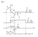
- FIG. 7 illustrates a driving waveform generated by a driving method of a plasma display apparatus according to a fifth embodiment
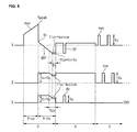
- FIG. 8 illustrates a driving waveform generated by a driving method of a plasma display apparatus according to a sixth embodiment.
- the plasma display apparatus includes a plasma display panel 100 and a driver for applying a predetermined driving voltage to electrodes of the plasma display panel 100.
- the driver includes a data driver 101, a scan driver 102, and a sustain driver 103.
- the scan driver 102 and the sustain driver 103 may correspond to a first driver.
- the data driver 101 may correspond to a second driver.
- the plasma display panel 100 includes a front panel (not illustrated) and a rear panel (not illustrated) which are coalesced at a given distance therebetween, and a plurality of electrodes.
- the plurality of electrodes include scan electrode Y1 to Yn, sustain electrodes Y, and address electrodes X1 to Xn.
- the plasma display panel 100 of the plasma display apparatus includes a front panel 200 and a rear panel 210 which are coupled in parallel opposite to each other at a given distance therebetween.
- the front panel 200 includes a front substrate 201 being a display surface on which an image is displayed.
- the rear panel 210 includes a rear substrate 211 constituting a rear surface.
- a plurality of scan electrodes 202 and a plurality of sustain electrodes 203 are formed on the front substrate 201.
- a plurality of address electrodes 213 are arranged on the rear substrate 211 to intersect the scan electrodes 202 and the sustain electrodes 203.
- the scan electrode 202 and the sustain electrode 203 each include transparent electrodes 202a and 203a made of transparent indium-tin-oxide (ITO) material, and bus electrodes 202b and 203b made of a metal material.
- the scan electrode 202 and the sustain electrode 203 generate a mutual discharge therebetween in one discharge cell, and maintain light-emissions of the discharge cells.
- the scan electrode 202 and the sustain electrode 203 are covered with one or more upper dielectric layers 204 for limiting a discharge current and providing insulation between the scan electrode 202 and the sustain electrode 203.
- a protective layer 205 with a deposit of MgO is formed on an upper surface of the upper dielectric layer 204 to facilitate discharge conditions.
- a plurality of stripe-type (or well-type) barrier ribs 212 are arranged in parallel on the rear substrate 211 of the rear panel 210 to form a plurality of discharge spaces (i.e., a plurality of discharge cells).
- the plurality of address electrodes 213 for performing an address discharge to generate vacuum ultraviolet rays are arranged in parallel to the barrier ribs 212.
- An upper surface of the rear panel 210 is coated with Red (R), green (G) and blue (B) phosphors 214 for emitting visible light for an image display during the generation of the address discharge is performed.
- a lower dielectric layer 215 is formed between the address electrodes 213 and the phosphors 214 to protect the address electrodes 213.
- FIG. 2 has illustrated and described only one example of the plasma display panel applicable to the embodiments, the embodiments are not limited to the structure of the plasma display panel illustrated in FIG. 2.
- FIG. 2 has illustrated the scan electrode 202 and the sustain electrode 203 each including the transparent electrode and the bus electrode.
- at least one of the scan electrode 202 and the sustain electrode 203 may include either the bus electrode or the transparent electrode.
- FIG. 2 has illustrated and described the structure of the plasma display panel, in which the front panel 200 includes the scan electrode 202 and the sustain electrode 203 and the rear panel 210 includes the address electrode 213.
- the front panel 200 may include all of the scan electrode 202, the sustain electrode 203, and the address electrode 213. At least one of the scan electrode 202, the sustain electrode 203, and the address electrode 213 may be formed on the barrier rib 212.
- the plasma display panel applicable to the embodiments has only to include the scan electrode 202, the sustain electrode 203, and the address electrode 210.
- the plasma display panel may have various structures as long as the above-described structural characteristics are satisfied.
- the scan driver 102 supplies a setup pulse and a set-down pulse to the scan electrode Y of the plasma display panel 100 during a reset period. Further, the scan driver 102 supplies a scan pulse to the scan electrode Y during an address period, and supplies a sustain pulse to the scan electrode Y during a sustain period.
- the sustain driver 103 supplies a sustain pulse to the sustain electrode Z during the sustain period.
- the scan driver 102 and the sustain driver 103 alternately operate during the sustain period.
- the data driver 101 supplies a data pulse to the address electrode X during the address period.
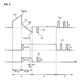
- FIG. 3 illustrates a driving waveform generated by a driving method of a plasma display apparatus according to a first embodiment.
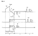
- FIG. 4 illustrates a driving waveform generated by a driving method of a plasma display apparatus according to a second embodiment.
- the driving method of the plasma display apparatus according to the first embodiment is performed with one subfield being divided into a reset period (R) during which the whole screen is initialized, an address period (A) during which scan lines are selected and discharge cells are selected from the selected scan lines, and a sustain period (S) during which a gray level is represented in accordance with the number of discharges.
- R reset period
- A address period
- S sustain period
- the reset period (R) is subdivided into a setup period (R_up) and a set-down period (R_dn).
- a setup pulse sup i.e., a first pulse gradually rising from a positive voltage to a peak voltage Vpeak is applied to the scan electrode Y.
- a weak discharge occurs inside the discharge cells of the whole screen such that wall charges are generated inside the discharge cells.
- a set-down pulse SDP (i.e., a second pulse) gradually falling from a positive first voltage V1, that is lower than the peak voltage Vpeak of the setup pulse SUP, to a negative set-down voltage -Vsd (i.e., a second voltage -V2) is applied to the scan electrode Y.
- a weak erase discharge occurs inside the discharge cells such that wall charges excessively generated prior to the generation of the weak erase discharge are erased. The remaining wall charges inside the discharge cells are uniform.
- a positive third voltage V3 is applied to the address electrode X in the first half of the set-down period (R_dn).
- the third voltage V3 may be substantially equal to a voltage Va (i.e., a data voltage Va) of a data pulse dp applied to the address electrode X during the address period (A) which follows the reset period (R).
- a voltage of the address electrode X floats for a predetermined time period of the set-down period (R_dn).
- the predetermined time period Td1 for which the voltage of the address electrode X floats ranges from 1 ⁇ s to 50 ⁇ s.
- a floating voltage of the address electrode X is output by turning off all of one or more switch elements (not illustrated) used to apply the data voltage Va and a ground level voltage to the address electrode X.
- a scan pulse sp of a negative polarity is applied to the scan electrode Y and, at the same time, the data pulse dp of a positive polarity is applied to the address electrode X.
- a positive fourth voltage V4 is applied to the sustain electrode Z during a set-down period (R_dn) and an address period (A).
- the fourth voltage V4 may be substantially equal to a voltage Vs (i.e., a sustain voltage Vs) of a sustain pulse sus applied to the sustain electrode Z during a sustain period (S).
- a voltage applied to the sustain electrode Z floats for a predetermined time period Td1 of the set-down period (R_dn).
- a floating voltage of the sustain electrode Z is output by turning off all of one or more switch elements (not illustrated) used to apply the sustain voltage Vs and a ground level voltage to the sustain electrode Z.
- a start time point at which the voltage of the sustain electrode Z floats may be substantially equal to a start time point at which the voltage of the address electrode X floats.
- a start time point at which all of the one or more switch elements used to apply the data voltage Va and the ground level voltage to the address electrode X are turned off may be equal to a start time point at which all of the one or more switch elements used to apply the sustain voltage Vs and the ground level voltage to the sustain electrode Z are turned off.
- Sustain pulses sus are alternately applied to the scan electrode Y and the sustain electrode Z during the sustain period (S) such that a sustain discharge occurs. An image is displayed on the plasma display panel through the sustain pulses sus.
- the voltage of the address electrode X floats for the predetermined time period Td1
- the voltage of the sustain electrode Z floats for the predetermined time period Td1. Therefore, a stable discharge occurs between the scan electrode Y and the address electrode X by preventing changes in a state of wall charges distributed in the address electrode X.
- FIG. 5 illustrates a driving waveform generated by a driving method of a plasma display apparatus according to a third embodiment.
- a voltage of the address electrode X floats for a predetermined time period Td2 of a set-down period (R_dn), and a floating voltage of the address electrode X is maintained at a predetermined voltage for a predetermined time period.
- the floating voltage of the address electrode X falls with the slope similar to the slope of the set-down pulse SDP and is then maintained at a predetermined voltage for the predetermined time period Ts.
- a peak portion of the set-down pulse SDP is flatly formed such that the floating voltage of the address electrode X has a flat bottom maintained at the predetermined voltage for the predetermined time period Ts. This results in the stabilization of wall charges formed inside the discharge cells.
- a voltage of the sustain electrode Z floats for the predetermined time period Td2 of the set-down period (R_dn).
- the floating voltage of the sustain electrode Z falls with the slope similar to the slope of the set-down pulse SDP, and is then maintained at a predetermined voltage for the predetermined time period Ts.
- the floating voltage of the sustain electrode Z has a flat bottom maintained at the predetermined voltage for the predetermined time period Ts.
- a set-down discharge i.e., an erase discharge
- a state of the wall charges distributed in the discharge cells is stable due to the set-down discharge such that a performance of an address discharge is improved.
- All of the scan electrode Y, the sustain electrode Z, and the address electrode X have the flat bottom for the predetermined time period Ts and the switch elements connected to the address electrode X are turned off during the set-down period (R_dn), thereby causing the voltage of the address electrode X to float.
- the quantity of light generated during the generation of the erase discharge is reduced by reducing the intensity of the erase discharge.
- FIG. 6 illustrates a driving waveform generated by a driving method of a plasma display apparatus according to a fourth embodiment.
- FIG. 7 illustrates a driving waveform generated by a driving method of a plasma display apparatus according to a fifth embodiment.
- FIG. 8 illustrates a driving waveform generated by a driving method of a plasma display apparatus according to a sixth embodiment. Since the driving waveforms illustrated in FIGs. 6 to 8 are equal to the driving waveforms illustrated in FIGs. 3 to 5 except a driving waveform during a setup period, the driving waveform during the setup period will be described in detail below.
- the driving method of the plasma display apparatus causes a voltage of the address electrode X to float by turning off a switch element connected to the address electrode X during a setup period (R_up).
- the voltage of the address electrode X floats by turning off a switch element used to apply a ground level voltage to the address electrode X.
- the voltage of the address electrode X rises due to a setup pulse sup (i.e., a first pulse) applied to the scan electrode X.
- the voltage of the address electrode X floats depending on a voltage of the scan electrode Y or the sustain electrode Z positioned opposite to the address electrode X.
- the voltage of the address electrode X has a rising waveform during the setup period (R_up).
- a floating voltage of the address electrode X does not rise to a voltage that is higher than the highest voltage (i.e., a data voltage Va) applied to the address electrode X, the floating voltage of the address electrode X rises from the ground level voltage to the data voltage Va corresponding to the setup pulse sup of the scan electrode Y.
- the voltage of the setup pulse sup is higher than the data voltage Va, the voltage of the address electrode X is clamped such that the voltage of the address electrode X no longer rise.
- the driving method of the plasma display apparatus improves the contrast characteristics by reducing the intensity of the discharge generated during the reset period, and improves the performance of the address discharge by stabilizing a state of wall charges distributed inside the discharge cells.
Landscapes
- Engineering & Computer Science (AREA)
- Physics & Mathematics (AREA)
- Power Engineering (AREA)
- Plasma & Fusion (AREA)
- Computer Hardware Design (AREA)
- General Physics & Mathematics (AREA)
- Theoretical Computer Science (AREA)
- Control Of Indicators Other Than Cathode Ray Tubes (AREA)
- Control Of Gas Discharge Display Tubes (AREA)
Applications Claiming Priority (1)
| Application Number | Priority Date | Filing Date | Title |
|---|---|---|---|
| KR1020060023591A KR100748989B1 (ko) | 2006-03-14 | 2006-03-14 | 플라즈마 디스플레이 장치의 구동 방법 |
Publications (2)
| Publication Number | Publication Date |
|---|---|
| EP1835481A2 true EP1835481A2 (de) | 2007-09-19 |
| EP1835481A3 EP1835481A3 (de) | 2007-10-10 |
Family
ID=38180618
Family Applications (1)
| Application Number | Title | Priority Date | Filing Date |
|---|---|---|---|
| EP07251049A Withdrawn EP1835481A3 (de) | 2006-03-14 | 2007-03-14 | Ansteuerverfahren für eine Plasmaanzeigevorrichtung |
Country Status (5)
| Country | Link |
|---|---|
| US (1) | US20070216608A1 (de) |
| EP (1) | EP1835481A3 (de) |
| JP (1) | JP2007249204A (de) |
| KR (1) | KR100748989B1 (de) |
| CN (1) | CN101038723A (de) |
Cited By (2)
| Publication number | Priority date | Publication date | Assignee | Title |
|---|---|---|---|---|
| WO2009040983A1 (ja) * | 2007-09-26 | 2009-04-02 | Panasonic Corporation | 駆動装置、駆動方法およびプラズマディスプレイ装置 |
| EP2246838A4 (de) * | 2008-02-27 | 2011-11-30 | Panasonic Corp | Vorrichtung und verfahren zum betreiben einer plasmaanzeigetafel und plasmaanzeigevorrichtung |
Families Citing this family (4)
| Publication number | Priority date | Publication date | Assignee | Title |
|---|---|---|---|---|
| KR20080092749A (ko) * | 2007-04-13 | 2008-10-16 | 엘지전자 주식회사 | 플라즈마 디스플레이 장치 |
| KR101121651B1 (ko) * | 2007-09-11 | 2012-02-28 | 파나소닉 주식회사 | 구동 장치, 구동 방법 및 플라즈마 디스플레이 장치 |
| JPWO2012102029A1 (ja) * | 2011-01-27 | 2014-06-30 | パナソニック株式会社 | プラズマディスプレイパネルの駆動方法およびプラズマディスプレイ装置 |
| JPWO2012102042A1 (ja) * | 2011-01-28 | 2014-06-30 | パナソニック株式会社 | プラズマディスプレイパネルの駆動方法およびプラズマディスプレイ装置 |
Family Cites Families (11)
| Publication number | Priority date | Publication date | Assignee | Title |
|---|---|---|---|---|
| JP3529737B2 (ja) * | 2001-03-19 | 2004-05-24 | 富士通株式会社 | プラズマディスプレイパネルの駆動方法および表示装置 |
| KR100502355B1 (ko) * | 2003-07-12 | 2005-07-21 | 삼성에스디아이 주식회사 | 어드레스 전극 라인들이 전기적으로 플로팅되는 플라즈마디스플레이 패널의 리셋팅 방법, 및 이 리셋팅 방법을사용한 플라즈마 디스플레이 패널의 구동 방법 |
| KR100515337B1 (ko) * | 2003-08-27 | 2005-09-15 | 삼성에스디아이 주식회사 | 플라즈마 디스플레이 패널의 구동 장치 및 구동 방법 |
| US7365710B2 (en) * | 2003-09-09 | 2008-04-29 | Samsung Sdi Co. Ltd. | Plasma display panel driving method and plasma display device |
| KR100570613B1 (ko) * | 2003-10-16 | 2006-04-12 | 삼성에스디아이 주식회사 | 플라즈마 디스플레이 패널과 그 구동방법 |
| KR100612333B1 (ko) * | 2003-10-31 | 2006-08-16 | 삼성에스디아이 주식회사 | 플라즈마 표시 장치와 플라즈마 표시 패널의 구동 장치 및구동 방법 |
| KR100524309B1 (ko) * | 2003-11-03 | 2005-10-28 | 엘지전자 주식회사 | 플라즈마 디스플레이 패널의 구동방법 |
| US20050225513A1 (en) * | 2004-04-02 | 2005-10-13 | Lg Electronics Inc. | Plasma display device and method of driving the same |
| KR100551013B1 (ko) * | 2004-05-21 | 2006-02-13 | 삼성에스디아이 주식회사 | 플라즈마 디스플레이 패널의 구동 방법 및 플라즈마 표시장치 |
| JP2005338784A (ja) * | 2004-05-28 | 2005-12-08 | Samsung Sdi Co Ltd | プラズマ表示装置とプラズマパネルの駆動方法 |
| KR20050121854A (ko) * | 2004-06-23 | 2005-12-28 | 삼성에스디아이 주식회사 | 2개의 구동부들만을 사용하는 플라즈마 디스플레이 패널의구동 방법 |
-
2006
- 2006-03-14 KR KR1020060023591A patent/KR100748989B1/ko not_active Expired - Fee Related
-
2007
- 2007-03-13 US US11/717,049 patent/US20070216608A1/en not_active Abandoned
- 2007-03-14 CN CNA200710085797XA patent/CN101038723A/zh active Pending
- 2007-03-14 EP EP07251049A patent/EP1835481A3/de not_active Withdrawn
- 2007-03-14 JP JP2007064671A patent/JP2007249204A/ja not_active Withdrawn
Cited By (4)
| Publication number | Priority date | Publication date | Assignee | Title |
|---|---|---|---|---|
| WO2009040983A1 (ja) * | 2007-09-26 | 2009-04-02 | Panasonic Corporation | 駆動装置、駆動方法およびプラズマディスプレイ装置 |
| US8416228B2 (en) | 2007-09-26 | 2013-04-09 | Panasonic Corporation | Driving device, driving method and plasma display apparatus |
| JP5275244B2 (ja) * | 2007-09-26 | 2013-08-28 | パナソニック株式会社 | 駆動装置、駆動方法およびプラズマディスプレイ装置 |
| EP2246838A4 (de) * | 2008-02-27 | 2011-11-30 | Panasonic Corp | Vorrichtung und verfahren zum betreiben einer plasmaanzeigetafel und plasmaanzeigevorrichtung |
Also Published As
| Publication number | Publication date |
|---|---|
| EP1835481A3 (de) | 2007-10-10 |
| CN101038723A (zh) | 2007-09-19 |
| US20070216608A1 (en) | 2007-09-20 |
| JP2007249204A (ja) | 2007-09-27 |
| KR100748989B1 (ko) | 2007-08-13 |
Similar Documents
| Publication | Publication Date | Title |
|---|---|---|
| EP1835481A2 (de) | Ansteuerverfahren für eine Plasmaanzeigevorrichtung | |
| KR100551033B1 (ko) | 플라즈마 디스플레이 패널의 구동 방법, 플라즈마디스플레이 패널의 구동 장치 및 플라즈마 표시 장치 | |
| CN100416631C (zh) | 用于驱动等离子体显示板的设备和方法 | |
| CN100552759C (zh) | 等离子显示设备 | |
| KR100667360B1 (ko) | 플라즈마 디스플레이 장치 및 그의 구동 방법 | |
| KR100508921B1 (ko) | 플라즈마 디스플레이 패널 및 그 구동 방법 | |
| US7812788B2 (en) | Plasma display apparatus and driving method of the same | |
| US20070216603A1 (en) | Method of driving plasma display apparatus | |
| EP1835483A2 (de) | Ansteuerverfahren für eine Plasmaanzeigevorrichtung | |
| US20080191973A1 (en) | Method of driving plasma display apparatus | |
| CN100392699C (zh) | 等离子显示面板的驱动方法 | |
| EP1887545A2 (de) | Aufrechterhaltungstreiber für eine Plasmaanzeigevorrichtung | |
| JP4029079B2 (ja) | プラズマディスプレイパネルの駆動方法とプラズマ表示装置 | |
| KR100482344B1 (ko) | 플라즈마 디스플레이 패널의 구동방법 | |
| KR100508237B1 (ko) | 플라즈마 디스플레이 패널의 구동방법 | |
| KR100606414B1 (ko) | 플라즈마 디스플레이 패널의 구동방법 | |
| EP1775698A1 (de) | Plasmaanzeigevorrichtung und Verfahren zu ihrer Ansteuerung | |
| US20080122817A1 (en) | Plasma display apparatus | |
| KR20040003247A (ko) | 플라즈마 디스플레이 패널의 구동방법 | |
| KR100710284B1 (ko) | 플라즈마 디스플레이 패널의 구동방법 및 구동장치 | |
| KR100649603B1 (ko) | 플라즈마 디스플레이 장치 | |
| US7733303B2 (en) | Plasma display apparatus and method of driving the same | |
| KR100560513B1 (ko) | 플라즈마 디스플레이 패널의 구동 방법 및 플라즈마 표시장치 | |
| KR20040098266A (ko) | 플라즈마 디스플레이 패널의 구동장치 및 구동방법 | |
| EP1833040A2 (de) | Plasmaanzeigevorrichtung und Verfahren zu ihrer Ansteuerung |
Legal Events
| Date | Code | Title | Description |
|---|---|---|---|
| PUAI | Public reference made under article 153(3) epc to a published international application that has entered the european phase |
Free format text: ORIGINAL CODE: 0009012 |
|
| PUAL | Search report despatched |
Free format text: ORIGINAL CODE: 0009013 |
|
| AK | Designated contracting states |
Kind code of ref document: A2 Designated state(s): AT BE BG CH CY CZ DE DK EE ES FI FR GB GR HU IE IS IT LI LT LU LV MC MT NL PL PT RO SE SI SK TR |
|
| AX | Request for extension of the european patent |
Extension state: AL BA HR MK YU |
|
| AK | Designated contracting states |
Kind code of ref document: A3 Designated state(s): AT BE BG CH CY CZ DE DK EE ES FI FR GB GR HU IE IS IT LI LT LU LV MC MT NL PL PT RO SE SI SK TR |
|
| AX | Request for extension of the european patent |
Extension state: AL BA HR MK YU |
|
| 17P | Request for examination filed |
Effective date: 20080408 |
|
| 17Q | First examination report despatched |
Effective date: 20080508 |
|
| AKX | Designation fees paid |
Designated state(s): DE FR NL |
|
| STAA | Information on the status of an ep patent application or granted ep patent |
Free format text: STATUS: THE APPLICATION IS DEEMED TO BE WITHDRAWN |
|
| 18D | Application deemed to be withdrawn |
Effective date: 20100508 |