EP1835448B1 - Ic-marker mit bei trennung variierender funktion - Google Patents
Ic-marker mit bei trennung variierender funktion Download PDFInfo
- Publication number
- EP1835448B1 EP1835448B1 EP05793707.0A EP05793707A EP1835448B1 EP 1835448 B1 EP1835448 B1 EP 1835448B1 EP 05793707 A EP05793707 A EP 05793707A EP 1835448 B1 EP1835448 B1 EP 1835448B1
- Authority
- EP
- European Patent Office
- Prior art keywords
- tag
- separation
- function
- separable portion
- data
- Prior art date
- Legal status (The legal status is an assumption and is not a legal conclusion. Google has not performed a legal analysis and makes no representation as to the accuracy of the status listed.)
- Expired - Lifetime
Links
Images















Classifications
-
- G—PHYSICS
- G06—COMPUTING OR CALCULATING; COUNTING
- G06K—GRAPHICAL DATA READING; PRESENTATION OF DATA; RECORD CARRIERS; HANDLING RECORD CARRIERS
- G06K19/00—Record carriers for use with machines and with at least a part designed to carry digital markings
- G06K19/06—Record carriers for use with machines and with at least a part designed to carry digital markings characterised by the kind of the digital marking, e.g. shape, nature, code
- G06K19/067—Record carriers with conductive marks, printed circuits or semiconductor circuit elements, e.g. credit or identity cards also with resonating or responding marks without active components
- G06K19/07—Record carriers with conductive marks, printed circuits or semiconductor circuit elements, e.g. credit or identity cards also with resonating or responding marks without active components with integrated circuit chips
- G06K19/072—Record carriers with conductive marks, printed circuits or semiconductor circuit elements, e.g. credit or identity cards also with resonating or responding marks without active components with integrated circuit chips the record carrier comprising a plurality of integrated circuit chips
-
- G—PHYSICS
- G06—COMPUTING OR CALCULATING; COUNTING
- G06K—GRAPHICAL DATA READING; PRESENTATION OF DATA; RECORD CARRIERS; HANDLING RECORD CARRIERS
- G06K19/00—Record carriers for use with machines and with at least a part designed to carry digital markings
- G06K19/06—Record carriers for use with machines and with at least a part designed to carry digital markings characterised by the kind of the digital marking, e.g. shape, nature, code
- G06K19/067—Record carriers with conductive marks, printed circuits or semiconductor circuit elements, e.g. credit or identity cards also with resonating or responding marks without active components
- G06K19/07—Record carriers with conductive marks, printed circuits or semiconductor circuit elements, e.g. credit or identity cards also with resonating or responding marks without active components with integrated circuit chips
- G06K19/073—Special arrangements for circuits, e.g. for protecting identification code in memory
-
- G—PHYSICS
- G06—COMPUTING OR CALCULATING; COUNTING
- G06K—GRAPHICAL DATA READING; PRESENTATION OF DATA; RECORD CARRIERS; HANDLING RECORD CARRIERS
- G06K19/00—Record carriers for use with machines and with at least a part designed to carry digital markings
- G06K19/06—Record carriers for use with machines and with at least a part designed to carry digital markings characterised by the kind of the digital marking, e.g. shape, nature, code
- G06K19/067—Record carriers with conductive marks, printed circuits or semiconductor circuit elements, e.g. credit or identity cards also with resonating or responding marks without active components
- G06K19/07—Record carriers with conductive marks, printed circuits or semiconductor circuit elements, e.g. credit or identity cards also with resonating or responding marks without active components with integrated circuit chips
- G06K19/073—Special arrangements for circuits, e.g. for protecting identification code in memory
- G06K19/07309—Means for preventing undesired reading or writing from or onto record carriers
- G06K19/07372—Means for preventing undesired reading or writing from or onto record carriers by detecting tampering with the circuit
- G06K19/07381—Means for preventing undesired reading or writing from or onto record carriers by detecting tampering with the circuit with deactivation or otherwise incapacitation of at least a part of the circuit upon detected tampering
-
- G—PHYSICS
- G06—COMPUTING OR CALCULATING; COUNTING
- G06K—GRAPHICAL DATA READING; PRESENTATION OF DATA; RECORD CARRIERS; HANDLING RECORD CARRIERS
- G06K19/00—Record carriers for use with machines and with at least a part designed to carry digital markings
- G06K19/06—Record carriers for use with machines and with at least a part designed to carry digital markings characterised by the kind of the digital marking, e.g. shape, nature, code
- G06K19/067—Record carriers with conductive marks, printed circuits or semiconductor circuit elements, e.g. credit or identity cards also with resonating or responding marks without active components
- G06K19/07—Record carriers with conductive marks, printed circuits or semiconductor circuit elements, e.g. credit or identity cards also with resonating or responding marks without active components with integrated circuit chips
- G06K19/077—Constructional details, e.g. mounting of circuits in the carrier
- G06K19/0772—Physical layout of the record carrier
- G06K19/07726—Physical layout of the record carrier the record comprising means for indicating first use, e.g. a frangible layer
Definitions
- the present invention relates to an IC tag and more particularly to an IC tag including a separable function change means.
- the IC tag comprises an insulator, such as paper or plastic, on which an antenna and an IC chip are disposed.
- Fig. 8 One example of such system is shown in Fig. 8 .
- the IC tag typically includes a reader/writer unit 250 and an IC tag 200, as in the example of Fig. 8 .
- a contactless IC tag (RFIC tag) is proposed that comprises an IC 20 (210) and an antenna 201, the IC 20 (210) including an RF unit, a modulator/demodulation unit, and a data storage unit, which are not shown (see Patent Document 1, for example), where the reader/writer unit 250 and the IC tag 200 communicate with each other using radio wave.
- Fig. 9 shows a perspective view of a conventional IC tag.
- the IC tag which is an RFIC tag, comprises an insulating substrate 90 of paper or plastic, for example, on which the coil antenna 201 and the IC chip 210 are layered. Since the structure is so simple, such IC tag can be used for various applications as mentioned above.
- IC tags such as the RFIC tag described in the Background Art section are required to be small and lightweight.
- the circuit configuration of the IC mounted on the IC tag is desired to be simple; it has therefore been difficult to equip the IC tag with hardware or software for the prevention of data tampering, which would result in complicating the data circuit or require an increase in its size. Consequently, the data in conventional IC tags can be easily tampered with.
- an IC tag according to claim 1.
- an IC tag according to claim 26.
- the IC tag has separable portions.
- the function of the IC tag is changed, the function relating to limitations concerning the input of data to and the output of data from the IC tag, for example.
- Such limitations in data input and data output of the IC tag and the change in the function of the tag caused by the separation of the separable portions prevent the falsification of data in the IC tag.
- the limitations of data input and data output of the IC tag and the tag function can be easily changed manually without the use of a reader/writer unit, unlike conventional IC tags.
- the IC tag of the invention is provided with the following means:
- an IC tag according to claim 1.
- an IC tag according to claim 28.
- the IC tag has separable portions.
- the function of the IC tag is changed, the function relating to limitations concerning the input of data to and the output of data from the IC tag, for example.
- Such limitations in data input and data output of the IC tag and the change in the function of the tag caused by the separation of the separable portions prevent the falsification of data in the IC tag.
- the limitations of data input and data output of the IC tag and the tag function can be easily changed manually without the use of a reader/writer unit, unlike conventional IC tags.
- the IC tag of the invention is provided with the following means:
- the IC tag of the invention is based on the basic premise that a k-th function is realized by the IC tag as a whole.
- a k-th function is realized by the IC tag as a whole.
- the IC tag of Fig. 1 is composed of three portions; namely, separable portions A1 and A2, and a non-separable portion B (tag main body).
- the portions A1, A2, and B are equipped with IC1, IC2, and IC3, respectively; and, as an interface between the tag and the outside (a reader/writer unit with which the tag exchanges data), antenna 1, antenna 2, and antenna 3, respectively.
- IC1 (10) and IC2 (20) are linked via a signal line L1 for signal transmission between IC1 (10) and IC2 (20); IC2 (20) and IC3 (30) are linked via a signal line L2 for signal transmission between IC2 (20) and IC3 (30).
- the IC tag is wired in such a layout that when A1 is separated from the tag main body along a separating line 1 (5), the signal line L1 is also severed; similarly, when A2 is separated from the tag main body along a separating line 2 (6), the signal line L2 is also severed.
- Lines SL12, SL21, SL23, and SL32 connecting IC1, IC2, and IC3 to common GND are wired in such a layout as to straddle the separating boundary lines between A1 and A2 or between A2 and B so that SL12 and SL21 are severed upon separation of A1 from the tag main body, while SL23 and SL32 are severed upon separation of A2 from the tag main body.
- the lines SL12, SL21, SL23, and SL32 are used for the determination of separation of A1 or A2 portion based on the detection of a change in the impedance of any of the lines caused by severing.
- Fig. 2 is a perspective view illustrating the three-dimensional structure of the IC tag of Fig. 1 .
- the IC tag according to the present embodiment is disposed on an insulator substrate 90 of paper or plastic, for example.
- common GND 91 is provided, which grounds lines SL12, SL21, SL23, and SL32 as well as ICs 1, 2, and 3.
- Fig. 3 is a block diagram of an example of IC1 (10).
- IC1 (10) includes the following: a power supply circuit 11 for converting part of a received signal from the antenna 1 into electric power; a transmission/receiving circuit 12 for the reception and transmission of signals to and from the antenna 1, which is an external interface of the tag; a modulating circuit 13 for modulating encoded data; a demodulating circuit 14 for demodulating a received signal; an encoding/decoding circuit 15 for the encoding of transmission data and the decoding of reception data; a data processing circuit 1 (16) and a storage unit 1 (18) for processing data sent from the encoding/decoding circuit 15 or via signal line L1; a control circuit 1 (17) for controlling the operation of the data processing circuit 1 (16) and the storage unit 1 (18) depending on the state of the tag; and an A1 separation decision circuit 2 (19) for the portion A1 itself to determine whether or not it is separated from the portion A2.
- the power supply circuit 11 is connected to a common power supply line
- Fig. 4 shows an example of IC2 (20).
- IC2 (20) includes the following: a power supply circuit 11 for converting part of a received signal into an electric power; a transmission/receiving circuit 12 for the transmission and reception of a signal to and from the antenna 2, which is an external interface of the tag; a modulating circuit 13 for modulating encoded data; a demodulating circuit 14 for demodulating a received signal; an encoding/decoding circuit 15 for encoding and decoding of data; a data processing circuit 2 (21) for processing data; a storage unit 2 (23); a control circuit 2 (22) for controlling the operation of the data processing circuit 2 (21) and the storage unit 2 (23) depending on the state of the tag; an A1 separation decision circuit 1 (24) for the portion A2 to determine whether or not the portion A1 is separated from the portion A2; and an A2 separation decision circuit 2 (25) for the portion A2 to determine whether or not the portion A2 is separated from the portion B.
- a power supply circuit 11 for converting part
- Fig. 5 shows a functional block diagram of an example of IC3 (30).
- IC3 (30) includes the following: a power supply circuit 3 (11) for converting part of a received signal into electric power; a transmission/receiving circuit 12 for the transmission and reception of a signal to and from the antenna 3, which is an external interface of the tag; a modulating encoded data modulating circuit 13; a demodulating circuit 14 for demodulating a received signal; a encoding/decoding circuit 15 for encoding and decoding of data; a data processing circuit 3 (31) for processing data; a storage unit 3 (33); a control circuit 3 (32) for controlling the operation of the data processing circuit 3 (31) and the storage unit 3 (33) depending on the state of the tag; and an A2 separation decision circuit 1 34 for the portion B to determine whether or not the portion A2 has been separated from the portion B.
- a power supply circuit 3 (11) for converting part of a received signal into electric power
- a transmission/receiving circuit 12 for the transmission
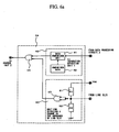
- Fig. 6a shows a functional block diagram of an example of the A1 separation decision circuit 1 (24) in the IC2 (40).
- the A1 separation decision circuit 1 (24) is composed of a separation decision circuit 1 (40) for the signal line L1 and an impedance change detection circuit 1 (50) for detecting a change in the impedance of the line SL21.
- Tables 1a to 1d are separation decision tables.
- the separation decision circuit 1 (40) for signal line L1 compares identification data sent from IC1 (10) via the signal line L1 against comparison data 42. If the identification data sent from IC1 via the signal line L1 agrees with the comparison data 42, as shown in Table 1a, the separation decision circuit outputs "0" ; if the identification data does not agree with the comparison data 42, it outputs "1".
- the impedance change detection circuit 1 (50) for detecting a change in the impedance of line SL21 determines whether or not the line SL21 is connected to the common GND. It outputs "0" if, as shown in Table 1a, the line SL21 is connected to common GND; it outputs "1” if the line SL21 is severed and in an open state.
- a method may be employed whereby data stored in IC1 (10) and IC2 (20) in advance are compared, the former as identification data and the latter as comparison data.
- a method may be employed whereby arbitrary comparison data is transmitted to IC1 (10) from IC2 (20) via the signal line L1; the arbitrary comparison data received by IC1 (10) is returned as identification data which is compared in the separation decision circuit 1 (40) for signal line L1.
- the output of the separation decision circuit 1 (40) signal line L1 and the output of the impedance change detection circuit 1 (50) are fed to the AND circuit 54 which calculates their logical AND, and that when logical AND is "1," it is determined that A1 is separated from the tag.
- the method of such decision is not limited to this. For example, a method may be adopted whereby it is determined that the portion A1 is separated from the tag main body when the logical OR of the output of the separation decision circuit 1 (40) for signal line L1 and the output of the impedance change detection circuit 1 (50) is "1"; namely, when either signal line L1 or line SL21 is severed.
- an OR circuit is used instead of the AND circuit 54.
- the following is a description of such operation with reference to the impedance change detection unit 50 for line SL21 shown in Fig. 6a as an example.
- the AND circuit 53 two inputs are made common. Until A1 is separated along the separating line 1, the line SL21 is not severed and so the two inputs to the AND circuit 53 are at GND potential.
- the two inputs to the AND circuit 53 are at "Low” and its output is "0.”
- the line SL21 is also severed, so that the potential of the two inputs to the AND circuit 53 is at "Hi” or R2 ⁇ Vcc/(R1+R2), and its output is "1.”
- the impedance change detection unit 50 can detect a change in the impedance of SL21 caused by the separation of A 1 along the separating line 1.
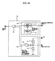
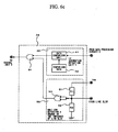
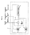
- the configuration of the remaining three separation decision circuits other than the A1 separation decision circuit 1 (24) are shown in Figs. 6b , 6c , and 6d , and their separation decision tables are shown in Tables 1b, 1c, and 1d.
- the configuration and operating principle of the above three separation decision circuits are basically the same as those of the above-described A1 separation decision circuit 1; therefore, their individual descriptions are omitted.
- Figs. 7a , 7b , and 7c show functional block diagrams of examples of the storage unit 1 (18), storage unit 2 (23), and storage unit 3 (33).
- the storage unit 1 (18) includes a write control circuit 61, a read control circuit 62, and a read-dedicating circuit 63 for a storage region 1 (64) from and to the data processing circuit 1 (16).
- the write control circuit 61 based on write request control data from control unit 1, records write data from the data processing circuit 1 (16), which is based on the first function of the IC tag, in the storage region 1 (64).
- the read-dedicating circuit 62 based on control data from the control circuit 1 (17) demanding read dedication, can prevent the writing of data in the storage region 1 (64). In this way, writing of data can be prevented and the storage region 1 (64) can be rendered dedicated to read-only purposes.
- the read control circuit 62 based on control data from the control unit 1 (17) demanding a readout, delivers the data stored in the recording region 1 (64) to a data processing unit 3 (31).
- Fig. 7b shows the configuration of the storage unit 2 in IC2.
- the storage unit 2 (23) is configured similarly to the storage unit 1 (18), and it carries out the writing process, reading process, and read-dedicating process with regard to the storage region 2 (65) on the basis of the second function.
- Fig. 7c shows an example of the storage unit 3 (33) of IC3.
- the storage unit 3 (33) carries out the write process, read process, and read-dedicating process similarly to the storage unit 1 (18).
- the storage unit 3 (33) is composed of a storage region 1 (64) and a storage region 2 (65) for recording the operation of the first function and the second function controlled by IC1 and IC2, in addition to the storage region 3 (66) 3 for recording the data based on the operation of the third function.
- IC tag processes are performed along the distribution process, as follows: 1) With the portion A1, portion A2, and portion B all ready, the tag is fed with data (which is stored in the storage unit), such as the product identification code, manufacturing number, date of manufacture, shipping date, and the like, and the tag is then affixed to a product; 2) Upon shipping from the factory, the portion A1 is separated from the tag, and the product is shipped to a distribution outlet. The thus separated portion A1 is left as a shipping source stub; 3) At the distribution outlet, data such as date of selling, name of distribution outlet, and the like is entered. This is followed by separating of the portion A2, and the product with the tag having only the portion B is handed to the purchaser.
- data which is stored in the storage unit
- the thus separated portion A2 is kept as a distribution outlet stub; 4)
- the tag with the sole portion B which is handed to the purchaser together with the product becomes a purchaser stub.
- Table 2 shows an example of the corresponding relationship between changes in the state of the tag and the resultant function changes in the tag in a case where the tag of the present embodiment is utilized for merchandise distribution management.
- IC1 upon shipping from the factory, IC1 (10) has the functions including: control of communication with the outside of the tag; communication with IC2 (20) and IC3 (30); designation of an address in the storage region 1 of the storage units 1 to 3; output of an instruction to write data 1 in the storage region 1 of the storage units 1 to 3; and write and read of data 1 in and out of the storage region 1 of the storage unit 1.
- IC1 carries out the first function for the input/output of data (data 1), including product identification code, manufacturing number, date of manufacture, and shipping date and the like.
- IC2 (20) has the functions for communication with IC1 and IC3; output of an instruction to prohibit writing in regions other than the storage region 1, to the storage unit 3 in IC3 (30); and writing of data 1 in the storage region 1 of the storage unit 2.
- IC3 (30) has the functions for communication with IC1 (10) and IC2 (20), and writing of data 1 in the storage region 1 of the storage unit 3.
- IC2 (20) has the functions for: communication with the outside of the tag; communication with IC3 (30); designation of an address in the storage region 2 of the storage units 2 and 3; writing and reading of data 2 in and out of the storage region 2 of the storage unit 2; and dedicating of the storage region I of the storage unit 2 for readout (read-only) purposes.
- IC2 (20) carries out the second function including the output of data 1 and the input/output of data (data 2) including date of selling and name of distribution outlet and the like.
- IC3 (30) carries out the functions for communication with IC2 (20); dedicating of the storage region 1 of the storage unit 3 for readout purpose; and writing of data 2 in the storage region 2 of the storage unit 3.
- IC(30) At the purchaser (after purchase), where the portions A1 and A2 are separated, IC(30), with A2 already separated, has the functions for: controlling communication with the outside of the tag; dedicating of the storage regions 1 and 2 of the storage unit 3 for readout (read-only) purposes; and writing/reading of data 3 in and out of the storage region 3 of the storage unit 3.
- IC3 (30) carries out the third function including the output of data 1 and data 2, and the input/output of arbitrary data (data 3), such as a memo by the purchaser.
- the read dedication process is carried out because it is preferable to disable some of the functions of the individual IC tags (such as the function of writing of information in a storage region dedicated for the particular tag) after a particular region has been separated.
- Table 3 Table 2 of the correspondence between changes in the function of the tag and the function of individual ICs Distribution step Factory (before shipping) Distribution outlet (shipping to sale) Purchaser (after purchase) State of tag No separation (A1, A2, and B are all there) A1 is separated (A2 and B remain) A2 is separated following A1 (only B remains)
- Function of tag Input/output of data data 1) including product ID code, manufacturing No., date of manufacture, and shipping date/time (first function) Output of data 1, and input/output of data (data 2) including date/time of sale, name of distribution store (second function) Output of data 1 and data 2, and input/output of arbitrary data (data 3) including memo by purchaser (third function)
- Function of IC1 Controls communication with the outside of tag; Communication with IC2
- control functions for realizing the first function may be shared by IC1 (10) and IC2 (20) and some of the control functions for realizing the second function may be shared by IC2 (20) and IC3 (30), as shown in Table 3. Further, the writing of data in the storage region 3 of the storage unit 3, which is the third function, may be blocked by IC2.
- IC1 (10) controls communication with, the outside of the tag; communicates with IC2 and IC3; outputs an instruction to write data 1 in the storage region 1 of the storage unit 1 to 3; and writes and reads data 1 in and out of the storage region 1 of the storage unit 1, while IC2 (20): communicates with IC1 and IC3; designates an address in the storage region 1 of the storage units 1 to 3; outputs to the storage unit 3 of IC3 an instruction prohibiting the writing of data in regions other than the storage region 1; and writes data 1 in the storage region 1 of the storage unit 2.
- some of the functions (first function) of IC1 (10) are carried out by IC2 (20).
- the tag When the functions for realizing any one of the functions are distributed among a plurality of ICs, as shown in Table 3, the tag would not operate normally if the order in which the tag including the ICs should be separated is disregarded, thus disabling the proper use of the tag and preventing unauthorized use.
- Table 4 shows the correspondence between changes in the state of the tag of the invention and resultant changes in the function of the tag when the IC tag of Fig. 1 is applied to the aforementioned distribution management, and the relationship between the information stored in each storage region of the storage units 1 to 3 and the state of each storage region.
- Table 4 with regard to the stored data in the storage region 1, for example, at the factory (before shipping), it is allowed to write and read data such as product identification code, manufacturing number, date of manufacture, and shipping date/time. In contrast, at the distribution outlet (after shipping and prior to sale), it is only allowed to read data such as product identification code, manufacturing number, date of manufacture, and shipping date.
- Table 5 shows the function of A1 and A2 as an IC tag after they are separated from the tag main body when the IC tag of Fig. 1 is applied to distribution management.
- the portions A1 and A2 are each independently equipped with an external interface and a power supply circuit, so that the portions A1 and A2 each include the function as an IC tag, as shown in Table 5, thus facilitating data management.
- the tag (A1) after separation is capable of controlling communication with the outside, dedicating the storage region 1 of the storage unit 1 for readout purpose, and reading the data 1 from the storage region 1 of the storage unit 1.
- the tag (A2) after separation is capable of controlling communication with the outside of the tag (A2), dedicating the storage regions 1 and 2 of the storage unit 2 for readout purpose, and reading the data 1 and 2 from the storage regions 1 and 2 of the storage unit 2.
- the tag (B) after separation is capable of controlling communication with the outside of the tag (B), dedicating the storage region 1 and 2 of the storage unit 3 for readout purpose, and writing/reading of the data 3 in and out of the storage region 3 of the storage unit 3.
- the foregoing embodiment has been described with reference to a contactless tag which exchanges information with the outside wirelessly, such as by using radio wave.
- the medium for such exchange of information is not limited to radio wave, however; for example, magnetism may be used.
- the type of the tag is not limited to the contactless type; for example, the tag may be of contact type.
- the configuration of the signal line Lk is not limited to such that the signal line straddles the separating line of the tag.
- a configuration may be adopted such that an electric signal connection is established between ICk and ICk+1 via inductive or capacitive coupling between line patterns disposed opposite each other with the separating line between them, where the coupling becomes weaker or is eliminated upon separation of the tag.
- a configuration may be adopted such that, instead of the severing of the line by the separation of the tag, the portion A and portion B of the tag are partially overlapped upon each other, where the electric connection is eliminated by separating such overlap.
- the overlapping portions may be affixed with adhesive taping or the like which can be peeled as needed.
- Fig. 10(a) shows a structure of the IC tag in which the insulating substrate 90 is provided with cutouts 93 (through-holes and/or cutouts at the edges) along the separating line 1 (5) and separating line 2 (6). In this way, separation of the separable portions A1 and A2 from the tag main body is made easier.
- Fig. 10(b) shows an IC tag in which the separation of A1 and A2 from the tag main body is made easier by forming the portions of the insulating substrate near the separating line 1 (5) between A1 and A2 and the separating line 2 (6) between A2 and B with a material 902 that is different from a substrate material 901 of the other portions of the insulating substrate.
- Possible combinations of the substrate materials 901 and 902 include: 1) 901: coated paper, and 902: non-coated paper; and 2) 901: vinyl material, and 902: paper material. This is, however, merely an example, and any combination may be used as long as the strength of the material 902 (tensile strength) is smaller than that of the material 901.
- Fig. 10(c) shows a layered IC tag composed of A1, A2, and B stacked vertically, as opposed to the horizontal connection of A1, A2, and B shown in Figs. 10(a) and 10(b) .
- the wires connecting A1, A2, and B are connected vertically with respect to the substrate in a connecting portion 105.
- the separation of A1 or A2 takes place in a peeling manner rather than in a separating manner.
- the separation of the tag is detected upon electric severing of the wires straddling between A1 and A2 and between A2 and B. Consequently, when the IC tag according to the present embodiment is actually affixed to a product, a part of the separating portion (i.e., the separating line portion of the tag) of the tag is subject to a potential separation unintended by the user.
- an IC tag of the invention provided with features to prevent such malfunction caused by a partial separation at the separating (line) portion of the IC tag is described.
- Fig. 12 shows an IC tag in which the width of line 101 connecting IC1 and IC2, which is used for the detection of separation of A1, is made substantially the same as the width of the tag near the perforated line for the separation of the tag along the separating line 1 (5), in view of the fact that an unintended severing tends to occur near the separating line 1 (5).
- Fig. 13 shows an IC tag in which the line 101 connecting IC1 and IC2 that is used for the detection of separation of A1 near the separating line 1 (5) is divided into a plurality of branches 101 b.
- the branch lines 101b intersect the separating line 1 (5) at a plurality of different locations.
- the IC tag of Fig. 13 is capable of maintaining the electrical connection of the line 101 even if the separating line 1 (5) is partly and unintentionally severed (at a location closer to the edge of the tag, for example), because such severing would involve only some of the branch lines 101b.
- the common power supply line and the like that are inherent are omitted in order to clarify the wiring layout of the line 103 used for the detection of A1 separation, which is one of the key points of the present invention.
- IC1 (10) and IC2 (20) of Fig. 14 are connected by lines 103, which are used for the detection of separation of A 1.
- the lines 103 have a connecting surface 104 on the side of A 1 facing B and a connecting surface 105 on the side of B facing A1, as shown in Figs. 15(a) and 15(b) , so that the lines 103 can have an increased area of connection.
- the common power supply line and the like that are inherent are omitted so as to clarify the wiring layout of line 106 and line 107, which are used for the detection of separation of A1 and constitute one of the key points of the invention.
- the layered IC tag of Fig. 16 is fabricated by layering the A1 layer shown in Fig. 17a on the B layer shown in Fig. 17b .
- the lines 106 and the lines 107 are each divided into three branch lines 106a, 106b, and 106c; and 107a, 107b, and 107c, respectively.
- the thus divided branch lines with the same numbers on the A1 and the B are connected to each other, respectively, by line connecting means, such as through-holes, provided in the insulator substrate of A1 in the connecting portion 150 thereof.
- Fig. 16 has the connecting portion 150 located at the left end
- the position of the connecting portion 150 is not particularly limited.
- the entire overlapping portions of the tag may be used as connecting surfaces.
- the wiring patterns according to present embodiment are all regularly and evenly arranged, they may be irregularly and/or unevenly arranged.
- Fig. 18 shows an IC tag different from the foregoing IC tag described with reference to Figs. 12 to 17 in which the technique to prevent malfunction in the tag separation determination caused by the partial separation at the separating portion (separating line portion of the tag) of the IC tag unintended by the user was applied.
- a line used for the separation determination is intentionally adapted to be severable readily.
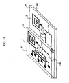
- lines 1010, 1020, and 1030 which are used for the determination of separation of A1 are arranged in a zigzag manner with respect to the separating line 1 (5) so as to increase the number and area of intersections between the separating line 1 (5) disposed on a substrate 90 and the lines 1010, 1020, and 1030.
- openings 1050 are intermittently provided along the separating line 1 (5).
- the openings 1050 make it possible to sever the lines (1010, 1020, and 1030), which are used for the determination of separation of A1, even when a small tear occurs along the separating line 1 (5) between A1 and B in response to the external application of force to the tag, thereby increasing the probability of electric severing between IC1 (10) and IC2 (20).
- Fig. 19 shows an IC tag adapted such that the line used for separation determination is intentionally adapted to be readily severed, wherein, as shown in Fig. 10(b) , the substrate material 902 of the tag near the separating line 1 (5) is different from the material 901 of the substrate at portions thereof other than the vicinity of the separating line 1.
- this IC tag is composed of A1 and B, which are connected via a separating portion 310 whose substrate material is 902. All of the lines connecting the tag A1 and the tag B pass the separating portion 310.
- a material is selected whose mechanical strength deteriorates more easily due to chemical reaction or the like than that of the substrate material 901.
- the mechanical strength of the substrate material 902 deteriorates, thereby enabling intentionally the line used for separation determination to be readily severed.
- Fig. 20 shows an application of the intended IC tag as a seal on a bottle where, as shown in Figs. 18 and 19 , the line used for separation determination is adapted to be readily severed.
- the IC tags 310, 313, and 315 are affixed such that they straddle both a bottle 305 and a cap 303.
- the IC tags are affixed such that, so as to ensure the detection of application of force to the cap 303 or the opening thereof, the separating line (310a, 313a, 315a) of the IC tag is aligned with the boundary between the bottle 305 and the cap 303.
- the substrate material 902 of the separating portion 310 may advantageously employ a material that dissolves upon reaction with the content of the container to which the IC tag is affixed, for the purpose of detecting the leakage of the content from the container, for example.
- Such IC tag where the line used for separation determination as shown in Fig. 20 is severed when opened, may be affixed to bottles, for example, whereby the data returned to a reader/writer device can be modified (i.e., the function of the IC tag is changed).
- bottles When such bottles are put in a packaging box 308, it becomes possible to determine the presence or absence of damage or leakage from the bottles by monitoring a change in the function of the IC tag used as a seal on the bottles without opening the packaging box 308.
- the IC in which the line used for separation determination is intentionally adapted to be severed readily has been described with reference to examples in which the wiring layout and the substrate material of the IC tag have been ingeniously designed.
- the IC tag in which the line used for separation determination is intentionally adapted to be severed readily may be realized in other ways.
- the line used for separation determination may be formed of conductive ink with little mechanical strength, or other material such as zinc or aluminum whose mechanical strength deteriorates or whose electric resistance increases due to chemical reaction such as corrosion.
- the information such as the access code for the confirmation of input/output of data, and a setting code for changing data input/output limitation, for example
- information 1 which comprises a one-dimensional barcode
- information 2 which comprises alphabets and numerals
- information 3 which comprises a two-dimensional barcode
- information 1 (401) is located on A1
- information 2 (402) is located on a top side of A2 (facing A1)
- information 3 (403) is located on a top side of B (facing A2).
- the following arrangements are also possible:
- the arrangement of information 2 and information 3 is not particularly limited as long as they both can be acquired only after at least the separable portions (A1, A2) of the tag are separated, depending on the configuration of the IC tag (in terms of the shape, size, and location of A1, A2, and B). Thus, the arrangement is not limited to as shown in Figs. 22, 23, and 24 , where information 2 (402) and information 3 (403) are both hidden by the separable portions of the tag.
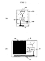
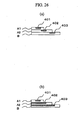
- information 2 (402) and information 3 (403) may be located such that they are partly visible even when. A1 and A2 are not separated, as shown in Fig. 26(a), (b) . Any of the individual items of information may be entirely visible.
- Information 1 is represented by a one-dimensional barcode, information 2 (402) by numerals and alphabets, and information 3 (403) by a two-dimensional barcode.
- information 1, information 2, information 3 may be represented in any way, such as in the form of machine-readable data, or numbers, characters, or symbols that can be read by humans. The information may be partly exposed on an upper layer.
- Fig. 28 shows an example of the content of the information 1 (401), information 2 (402), and information 3 (403) where the relationships of Table 4 are established between the state of the IC tag and its function by employing a reader/writer device that carries out a data read/write operation on the IC tag by means of the data read request signal and data write request signal having the data structure shown in Fig. 27 , and the IC tag of the invention of Fig. 21 .
- Fig. 28 shows the structure of information 1 (401), information 2 (402), and information 3 (403) in a case where data write access code (1305) and data read access code (1303) are all varied depending on the merchandise distribution management step (the separation state of the IC tag).
- the information 1 (401), information 2 (402), and information 3 (403) may be configured as shown in Fig. 29 when the tag ID (1301) and the data read access code (1303) are shared.
- the tag ID (1301) depending on the merchandise management step (the separation state of the IC tag), and where A1, A2 and B separated from the tag main body are operated as independent tags. Unless the A1 and A2 separated from the tag main body are used as independent IC tags, the tag ID (1301) of information 1, the tag ID (1303) of information 2, and the tag ID (1305) of information 3 may all be the same.
- the tag ID (1301), data write access code (1305), and data read access code (1303) in accordance with the merchandise management step (the separation state of the IC tag) are written in the individual ICs in the IC tag upon fabrication of the IC tag as described below.
- information 1, information 2, and information 3 may be first affixed to A1, A2, and B, and then A1, A2, B may be layered, followed by the connecting of all the lines and the writing of information 1, information 2, and information 3 in the individual ICs of A1, A2, and B.
- the confirmation of the state of the IC tag in step 213 is based on the result of determination made by a B-separation decision circuit 2 in IC2 and the result of determination made by an A1-separation decision circuit 1 in IC2.
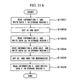
- Fig. 31b shows a flowchart of a process during the course of merchandise distribution using the IC tag according to the present embodiment.
- IC tag according to the present embodiment has been made with reference to examples where the form or structure of data stored or exchanged with the external reader/writer is fixed in one particular kind.
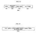
- data formats for IC tags such as the Auto-ID data format shown in Fig. 32 (96-bit EPC code system) and the ubiquitous ID (128-bit ucode) shown in Fig. 33 , for example. Therefore, there has been a need for an IC tag whose data format can be modified in a simple manner depending on purposes or the kind of information.
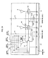
- the configuration of the IC tag of Fig. 34 is the same as that of the IC tag described with reference to Fig. 1 with the exception of the separable portion A1 which is provided with the initial setting means.
- the initial setting means provided with in the separable portion A1 shown in Fig. 34 comprises lines S1, S2, S3, and S4 running from the IC1 (10), each connected to a common power supply line 4, and cutout lines C1 to C4 that intersect the lines S1, S2, S3, and S4.
- These cutout lines C1 to C4 define cutouts that can be easily cut away by humans.
- the cutout lines C 1 to C4 are designed such that:
- Fig. 35 shows a perspective view of the structure of the IC tag of Fig. 34 which is formed on an insulator, such as paper or plastic.
- the cutout lines C1 to C4 have through-holes formed intermittently between the top surface and the bottom surface of the insulating substrate 90. Thus, any of the cutout lines C1 to C4 can be severed as desired by the user.
- Fig. 36 shows a functional block diagram of an example of the IC1 (10) of Fig. 34 .
- the data processing circuit 1 in IC 1 (10) has inputs associated with the individual lines S1 to S4, and is configured such that the input potential to the data processing circuit 1 via S 1 to S4 is changed depending on the presence or absence of severing of the lines S 1 to S4 by the cutout lines C1 to C4.
- the input potential of at least one of the inputs S1 to S4 to the data processing circuit 1 of Fig. 36 changes from "H" to "L", thereby entering an IC-tag type setting mode.
- the type of data format used by the IC tag is determined by the input potential of the inputs S1 to S2 to the data processing circuit 1.
- the IC1 then notifies of the data format the other ICs (IC2, IC3) in the tag.
- data formats and processing programs that are stored in the storage circuit 1 (18) in advance may be selected depending on the combination of the input potentials of S1 to S4 to the data processing circuit 1.
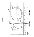
- This IC tag includes a non-separating portion B located at the center, around which separable portions A1 to An are arranged, where ICk of the separable portions and ICn+1 of the non-separable portion B are electrically connected.
- the number n of the separable portions from the tag main body (B) is 2.
- the IC tag of Fig. 37 differs from the IC tag of Fig. 1 in the following respects:
- the lines SL13, SL31, SL23, and SL32 connecting IC1 (10), IC2 (20), and IC3 (30) to the common GND are wired in such a layout that the lines straddle a separation boundary line between portion A1 and portion B or a separation boundary line between portion A2 and portion B, so that the lines SL13 and SL31 are severed when the A1 portion is separated and the lines SL23 and SL32 are severed when the A2 portion is separated.
- the lines SL13, SL31, SL23, and SL32 are used for detecting a change in the impedance of the lines caused by the severing of the lines so as to determine whether or not the A1 portion or the A2 portion is separated.
- Fig. 39 shows a perspective view of an IC tag corresponding to the structure of Fig. 37 .
- Fig. 40 shows a functional block diagram of IC1.
- IC1 (10) includes: a power supply circuit 11 for converting part of a received signal into electric power; a receiving circuit 12 for the transmission and reception of a signal to and from an antenna I, which is an external interface of the tag; a modulating circuit 13 for modulating encoded data; a demodulating circuit 14 for demodulating a received signal; an encoding/decoding circuit 15 for the encoding of transmission data and decoding of received data; a data processing circuit 1 (16) for processing data sent from the encoding/decoding circuit 15 or via the signal line L1; a storage unit 1 (18); a control circuit 1 (17) for controlling the operation of the data processing circuit 1 (16) and the storage unit 1 (18) depending on the state of the tag; and an A1 separation decision circuit 1 (19) for the portion A1 to determine whether or not the portion A1 has been separated from the portion B.
- Fig. 41 shows a functional block diagram of an example of the configuration of IC2 (20).
- IC2 (20) includes: a power supply circuit 11 for converting part of a received signal into electric power; a transmission/receiving circuit 12 for the transmission and reception of a signal to and from an antenna 2, which is an external interface of the tag; a modulating circuit 13 for modulating encoded data; a demodulating circuit 14 for demodulating a received signal; an encoding/decoding circuit 15 for encoding and decoding of data; a data processing circuit 2 (21) for processing data; a storage unit 2 (23); a control circuit 2 (22) for controlling the operation of the data processing circuit 2 (21) and the storage unit 2 (23) depending on the state of the tag; and an A2 separation decision circuit 1 (24) for the portion A2 itself to determine whether or not the portion A2 has been separated from the portion B.
- a power supply circuit 11 for converting part of a received signal into electric power
- a transmission/receiving circuit 12 for the transmission
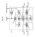
- Fig. 42 shows a functional block diagram of an example of the configuration of IC3 (30).
- IC3 (30) constitutes a central core of the IC tag according to the present embodiment, and it centrally controls the IC1 (10) and IC2 (20) in the two separable portions.
- IC3 (30) includes: a power supply circuit 11 for converting part of a received signal into electric power; a transmission/receiving circuit 12 for the transmission and reception of a signal to and from an antenna 3, which is an external interface of the tag; a modulating circuit 13 for modulating encoded data; a demodulating circuit 14 for demodulating a received signal; an encoding/decoding circuit 15 for encoding and decoding of data; a data processing circuit 3 (31) for processing data; a storage unit 3 (33); a control circuit 3 (32) for controlling the operation of the data processing circuit 3 (31) and the storage unit 3 (33) depending on the state of the tag; an A1 separation decision circuit 2 (34) for the portion B to determine whether or not the portion A1 has been separated from the portion B; and an A2 separation decision circuit 2 (35) for the portion B to determine whether or not the portion A2 has been separated from the portion B.
- the number of the separation decision circuits is increased.
- the configuration of the storage unit 1 (18), storage unit 2 (23), and storage unit 3 (23) of IC1 (10), IC2 (20), and IC3 (30) may be the same as shown in Figs. 7a , 7b , and 7c when the order of separation of the separable portions is predetermined as in A1, A2.
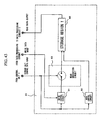
- the storage unit 2 of IC2 (20) may be configured as shown in Fig. 43 .
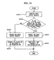
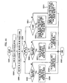
- Fig. 44 shows a flowchart of the flow of a process regarding an IC tag of the present embodiment in which the order of separation of the separable portions is not predetermined.
- the IC tag receives in step S2002 a request from the reader/writer.
- the ID code contained in the request signal data is confirmed.
- step S2004 a decision is made as to whether the ID code is associated with A1, A2, or B. If the decision points to A1, the process proceeds to step S2005, where it is determined whether or not B and A1 are connected.
- step S2006 data read and write requests with respect to the storage region 1 are followed, and then the process ends (step S2007). If the result of the determination in step S2005 is NO, the process proceeds to step S2008, where a data read request is followed but a write request is rejected with respect to the storage region 1; the process then proceeds to step S2007.
- step S2004 it is determined in step S2009 whether or not B and A2 are connected. If they are (YES), the process proceeds to step S2010, where data read and write requests with respect to the storage region 2 are followed, and then the process proceeds to step S2007. If NO, the process proceeds to step S2011, where a data read request with respect to the storage region 2 is followed but a write request is rejected; and then the process proceeds to step S2007.
- step S2004 the process proceeds to step S2012 where it is determined if there is only B. If there is only B (YES), the process proceeds to step S2013, where a data read request with respect to the storage regions 1 and 2 are followed but a write request is rejected, and where a data read/write request with respect to the storage region 3 is followed, and then the process proceeds to step S2007. If NO, the process proceeds to step S2014, where a data read request is followed but a write request is rejected with respect to the storage regions 1 and 2 and where data read and write requests are rejected with respect to the storage region 3; the process then proceeds to step S2007. As shown in Fig.
- the IC tag can be used regardless of the order of separation of Ak, by designating the utilized function of the IC tag and its corresponding tag using the ID code (information for selecting/designating the function of the IC tag).
- the non-separable portion B centrally manages (controls) the ICs (IC1 to ICn) of the separable portions A1 to An.
- Fig. 45 shows an example of the configuration of coupon tickets in which the IC tags of the present embodiment are utilized.
- the figure shows a top view so that the shape can be easily recognized.
- the IC tag main body lies in a portion B, which, using the portion B as a hub, centrally manages the other separable portions A1 to A5.
- the coupon tickets utilizing the IC tags which are often used in amusement parks and the like, are arranged in a plane such that they form a separable set of tickets from which one ticket is separated each time an attraction is purchased.
- the portions A1 to A5 each carry, as coupon IC tags, a coupon code in their storage regions that can be identified by individual coupon tickets.
- the user's profile information is set in the storage regions of the portions A1 to A5 and the tag main body B in an initializing process.
- the user's profile information herein refers to the kind of information that permits the analysis of the coupon user's tendencies, such as sex, age, and occupation.
- the portion A1 remains at the store, it becomes possible for the shop to monitor and analyze the tendencies of the customers based on the user profile information recorded in the recording unit in the portion A1, by putting the collected IC tags through a tag reader.
- the shop can utilize such information for marketing strategy planning purposes, for example.
- the tag main body B can detect and store the order of separation of the partial tags, such as A1, B, A5, A2, and A4.
- the order in which the coupon tickets were used can also be known by placing the tag main body B over the reader/writer.
- the configuration is simplified as compared with the case where tags are connected in series and a terminal tag of them functions as the tag main body. Further, since the tag main body B functions as a hub and manages the other coupon tickets A1 to A5, the tags A1 to A5 can be separated in any order.
- the invention has been described with reference to coupon tickets, the invention can be applied to any other purposes as long as they involve similar functions.
- the invention can be applied to tourist tickets that are used by tourists visiting many locations, or various other tickets for amusement parks and the like.
- the shape of the IC tag that has been described with reference to Fig. 9 is merely an example and any other shape may be adopted as long as Ak is connected via B.
- the IC tag of the invention can be used for various purposes regardless of the order of separation of Ak.
- the IC tag of the invention has excellent security against data tampering.
- the IC tag makes it possible to easily monitor the distribution history of each item of merchandise.
- a change in the function of the IC tag associated with the separation of the separable portions can be used for the confirmation of the presence or absence of damage to the item.
- the IC tag of the invention can be used for a wide variety of applications, such as a merchandise distribution management system, an inventory management system, a quality control system, an anti-theft system, and electronic tickets.
Landscapes
- Engineering & Computer Science (AREA)
- Computer Hardware Design (AREA)
- Microelectronics & Electronic Packaging (AREA)
- Physics & Mathematics (AREA)
- General Physics & Mathematics (AREA)
- Theoretical Computer Science (AREA)
- Computer Security & Cryptography (AREA)
- General Engineering & Computer Science (AREA)
- Credit Cards Or The Like (AREA)
- Burglar Alarm Systems (AREA)
Claims (39)
- IC-Tag mit einer Anzahl von n abtrennbaren Anteilen A1 bis An, wobei n eine natürliche Zahl ist, so dass n ≥ 1, und einem von den abtrennbaren Antcilen A1 bis An verschiedenen Anteil B,
wobei der abtrennbare Anteil Ak ein ICk (10) enthält und der Anteil B ein ICn+1 (30) enthält, wobei k eine natürliche Zahl ist, so dass 1 ≤ k ≤ n,
wobei das IC-Tag dadurch gekennzeichnet ist, dass es ferner eine Signalleitung Lk enthält, die das ICk (10) und das ICk+1 (20) elektrisch verbindet, wobei die Signalleitung Lk, die eine elektrische Signalverbindung zwischen dem ICk (10) und dem ICk+1 (20) bildet, nach der Abtrennung des abtrennbaren Anteils Ak unterbrochen ist, wobei jedes IC (10, 20, 30) eine Kommunikationseinheit, die ausgelegt ist, eine externe Kommunikationsfunktion für die Kommunikation nach außen bereitzustellen, und eine Steuereinheit zum Steuern der Kommunikationseinheit enthält,
wobei jedes Mal, wenn der abtrennbare Anteil Ak nacheinander von A1 bis An getrennt wird, die Abtrennung des abtrennbaren Anteils Ak detektiert wird, und die Funktion des Tags nacheinander von einer ersten Funktion zu der n+1-sten Funktion geändert wird und der abgetrennte abtrennbare Anteil Ak als ein unabhängiges IC-Tag arbeitet, indem er seine externe Kommunikationsfunktion beibehält. - IC-Tag nach Anspruch 1, wobei das ICk (10) einzeln die k-te Funktion hat und das ICn+1 (30) die n+1-te Funktion hat.
- IC-Tag nach Anspruch 1, wobei das ICk (10) und mindestens eines der ICk+1 (20) bis ICn+1 (30) eine Funktion zum Realisieren der k-ten Funktion gemeinsam nutzen.
- IC-Tag nach Anspruch 1, wobei das ICk (10) eine unabhängige Funktion hat und das ICk (10) und mindestens eines der ICk+1 (20) bis ICn+1 (30) eine Funktion zum Realisieren der k-ten Funktion gemeinsam nutzen.
- IC-Tag nach einem der Ansprüche 1 bis 4, wobei ein beliebiges der ICI bis ICk (10), die mindestens ICk (10) enthalten, die Funktion des Beschränkens des Ausdrucks der k+1-ten Funktion des Tags als Ganzes besitzt.
- IC-Tag nach einem der Ansprüche 1 bis 5, wobei der abtrennbare Anteil Ak eine Speichereinheit Mk (18) enthält und der Anteil B eine Speichereinheit Mn+1 (33) enthält, wobei die Speichereinheit Mk (18) einen Speicherbereich (64) zum Speichern von mindestens einem durch das Tag anhand der ersten Fünktion bis zu der k-ten Funktion erhaltenen Datenelement besitzt,
wobei die Speichereinheit Mn+1 (33) einen Speicherbereich (64; 65; 66) zum Speichern von mindestens einem durch das Tag anhand der ersten bis zu der n+1-ten Funktion erhaltenen Datenelement besitet. - IC-Tag nach Anspruch 6, wobei die ICk (10) bis ICn+1 (30) eine lesebestimmende Schaltung (63) enthalten, um nach der Abtrennung des abtrennbaren Anteils Ak die Bereiche der Speichereinheit Mk (18) bis Mn+1 (33) zum Speichern der anhand der k-ten Funktion erhaltenen Daten zum Lesen zu bestimmen.
- IC-Tag nach einem der Ansprüche 1 bis 7, wobei der abtrennbare Anteil Ak enthält:eine Lk-Durchtrennungsdetektionseinheit (40) zum Detektieren einer Durchtrennung in der Leitung Lk; undeine Ak-Durchtrennungsbestimmungseinheit (19), die das Ergebnis der Detektion des Vorhandenseins oder des Nichtvorhandenseins einer Durchtrennung in der Signalleitung Lk für eine Bestimmung der Durchtrennung des abtrennbaren Anteils Ak verwendet.
- IC-Tag nach Anspruch 8, wobei die Ak-Durchtrennungsbestimmungseinheit (19) eine Einheit enthält, um nach dem Bestimmen, dass der abtrennbare Anteil Ak abgetrennt worden ist, einen Datenspeicherbereich der Speichereinheit Mk (18), der den Daten, die durch mindestens die erste bis k-te Funktion erhalten werden, zugewiesen ist, zum Lesen zu bestimmen.
- IC-Tag nach Anspruch 9, wobei die Lk-Durchtrennungsdetektionseinheit (40) des abtrennbaren Anteils Ak die Durchtrennung der Signalleitung Lk anhand des Vorhandenseins oder des Nichtvorhandenseins eines Signals von ICk+1 (20) detektiert.
- IC-Tag nach Anspruch 10, mit:einer Impedanzänderungsdetektionseinheit (50) zum Detektieren einer Änderung in der Impedanz einer Leitung, die die zwei Bereiche, die den abtrennbaren Anteil Ak und den abtrennbaren Anteil Ak+1 enthalten, überspannt und die nach der Abtrennung des abtrennbaren Anteils Ak von dem Tag durchtrennt wird; undeine Ak-Abtrennungsdetektionseinheit (19) zum Bestimmen der Abtrennung des abtrennbaren Anteils Ak anhand des Ergebnisses der durch die Lk-Durchtrennungsdetektionseinheit (40) und die Impedanzänderungsdetektionseinheit (50) gemachten Bestimmungen.
- IC-Tag nach Anspruch 1, wobei der abtrennbare Anteil Ak+1 enthalt:eine Lk-Durchtrennungsdetektionseinheit (40) zum Detektieren der Durchtrennung der Signalleitung Lk, undeine Ak-Durchtrennungsbestimmungseinheit (24), die das Ergebnis des Detektierens des Vorhandenseins oder des Nichtvorhandenseins einer Durchtrennung der Signalleitung Lk für die Bestimmung einer Abtrennung des abtrennbaren Anteils Ak verwendet,wobei die Lk-Durchtrennungsdetektionseinheit (40) des abtrennbaren Anteils Ak+1 die Abtrennung der Signalleitung Lk anhand des Vorhandenseins oder des Nichtvorhandenseins eines Signals von ICk (10) bestimmt.
- IC-Tag nach Anspruch 12, wobei der abtrennbare Anteil Ak+1 enthält:eine Impedanzänderungsdetektionseinheit (50) zum Detektieren einer Änderung in der Impedanz einer Leitung, die die zwei Bereiche, die den abtrennbaren Anteil Ak und den abtrennbaren Abschnitt Ak+1 enthalten, überspannt und die durchtrennt wird, wenn der abtrennbare Anteil Ak von dem Tag abgetrennt wird,wobei die Ak-Durchtrennungsbestimmungseiheit (24) die Abtrennung des abtrennbaren Anteils Ak anhand des Ergebnisses der durch die Lk-Durchtrennungsdetektionseinheit (40) und die Impedanzänderungsdetektionseinheit (50) durchgeführten Detektion bestimmt.
- IC-Tag nach Anspruch 1, wobei die Informationen Ck+1 (402) nach der Abtrennung des abtrennbaren Anteils Ak erhältlich werden.
- IC-Tag nach Anspruch 14, wobei die Information Ck+1 (402) Informationen sind, die zum Aktivieren von mindestens einer der k+1-ten Funktion bis zu der n+1-ten Funktion des Tags notwendig sind.
- TC-Tag nach Anspruch 14 oder 15, wobei die Informationen Ck+1 (402) in einem elektrisch oder mechanisch lesbaren Codeformat oder in einem Format, das durch Menschen gelesen werden kann, das Zahlen, Buchstaben und/oder Symbole enthält, angegeben sind.
- IC-Tag nach Anspruch 16, wobei die Informationen Ck+1 (402) an einer Position angegeben sind, so dass sie nur erlangt werden können, nachdem der abtrennbare Abschnitt Ak abgetrennt wurde.
- IC-Tag nach Anspruch 17, das eine Struktur aufweist, so dass mindestens ein Teil des abtrennbaren Anteils Ak auf einem abtrennbaren Anteil Am oder dem Anteil B geschichtet ist, wobei m eine natürliche Zahl ist, so dass k < m ≤ n; und
wobei die Informationen Ck+1 (402) auf dem abtrennbaren Anteil Ak oder an einem Anteil der Anteils B, der durch den abtrennbaren Anteil Ak verdeckt ist, angegeben sind. - IC-Tag nach Anspruch 1, das eine Leitung (101) enthält, die für die Bestimmung der Abtrennung des abtrennbaren Anteils Ak, der von dem Tag nach der Abtrennung von dem Tag elektrisch getrennt wird, verwendet wird,
wobei die für die Abtrennungsbestimmung verwendete Leitung (101) ein erstes Verdrahtungsmuster besitzt, so dass keine elektrische Abtrennung in der für die Abtrennungsbestimmung verwendeten Leitung (101) auftritt, nur weil ein Teil des abtrennbaren Abschnittes Ak von dem Tag entlang der Trennlinie durchtrennt ist. - IC-Tag nach Anspruch 19, das das erste Verdrahtungsmuster enthält, das derart angeordnet ist, dass die für die Abtrennungsbestimmung verwendeten Zweigleitungen (101b) und die für die Abtrennungsbestimmung verwendeten Leitungen (101) die Trennlinie des abtrennbaren Anteils Ak an mehreren Stellen kreuzen.
- IC-Tag nach Anspruch 19, wobei die Breite der für die Ak-Abtrennungsbestimmung verwendeten Leitung im Wesentlichen gleich der Länge der Trennlinie an der und in der Nähe der Trennlinie ist.
- IC-Tag nach Anspruch 1 mit:einen Trennlinie zum Abtrennen des abtrennbaren Anteils Ak von dem Tag und einer Linie, die für die Bestimmung der Abtrennung des abtrennbaren Anteils Ak, der von dem Tag nach der Abtrennung von dem Tag elektrisch abgetrennt wird, verwendet wird,wobei das IC-Tag ein zweites Verdrahtungsmuster enthält, in dem sich die elektrische Abtrennung in der für die Ak-Abtrennungsbestimmung verwendeten Leitung einfach nach der Abtrennung eines Teils des abtrennbaren Anteils Ak von dem Tag entlang der Trennlinie entwickelt.
- IC-Tag nach Anspruch 22, wobei das zweite Verdrahtungsmuster derart angeordnet ist, dass die Trennlinie (5) und die für die Abtrennungsbestimumg des abtrennbaren Anteils Ak verwendete Linie (1000) einander wiederholt kreuzen.
- IC-Tag nach Anspruch 1, wobei der abtrennbare Anteil A1 oder der Anteil B enthält:eine Anfangseinstellungssicherheitsleitung (C1, C2, C3, C4) für die Anfangseinstellung des IC-Tags; undMittel (S1, S2, S3, S4) zum Detektieren des Vorhandenseins oder des Nichtvorhandenseins einer Durchtrennung in der Sicherheitsleitung,
- IC-Tag nach Anspruch 24, das mehrere der Anfangseinstellungssicherheitsleitungen (S1, S2, S3, S4) enthält, wobei eine unterschiedliche Amfangseinstellung abhängig davon, in welche der Sicherheitsleitungen (S1, S2, S3, S4) geschnitten wurde, gemacht wird.
- IC-Tag, das eine Anzahl von n abtrennbaren Anteilen A1 bis An, wobei n eine natürliche Zahl ist, so dass n ≥ 1, und einen von den abtrennbaren Anteilen A1 bis An verschiedenen nicht abtrennbaren Anteil B enthält, wobei jeder abtrennbare Anteil Ak ein ICk (10; 20) enthält und der nicht abtrennbare Anteil B ein ICn+1 (30) enthält, wobei k eine natürliche Zahl ist, so dass 1 ≤ k ≤ n,
wobei das IC-Tag dadurch gekennzeichnet ist,
dass der abtrennbare Anteil Ak eine Speichereinheit Mk (18; 23) enthält, wobei die Speichereinheit Mk (23) einen Bereich (65) zum Speichern von durch mindestens die k-te Funktion erhaltenen Daten enthält, wobei das IC-Tag ferner gekennzeichnet ist durch
eine Signalleitung Lk, die das ICk (10; 20) und das ICn+1 (30) elektrisch verbindet, wobei die Signalleitung Lk, die eine elektrische Signalverbindung wischen dem ICk (10; 20) und dem ICn+1 (30) bildet, nach der Abtrennung des abtrennbaren Anteils Ak durchtrennt ist, wobei der Anteil B eine Ak-Abtrennungsdetektionseinheit (34; 35) enthält, und die Funktion des Tags abhängig davon, ob der abtrennbare Anteil Ak von dem Tag abgetrennt wurde, geändert wird,
und wobei der abtrennbare Abschnitt Ak eine Funktion zum Kommunizieren nach außen enthält, wobei die Kommunikationsfunktion selbst dann beibehalten wird, wenn der abtrennbare Anteil Ak abgetrennt wurde, so dass das IC-Tag arbeiten kann. - IC-Tag nach Anspruch 26, wobei jedes Mal, wenn der abtrennbare Anteil Ak nacheinander in der Reihenfolge von A1 bis An abgetrennt wird, die Abtrennung des abtrennbaren Anteils Ak detektiert wird und die Funktion des Tags sich nacheinander von der ersten Funktion zu der n+1-ten Funktion ändert.
- IC-Tag nach Anspruch 27, wobei das ICk (10; 20) die k-te Funktion einzeln beaufsichtigt und das ICn+1 (30) die n+1-te Funktion beaufsichtigt.
- IC-Tag nach Anspruch 27, wobei mindestens einen der ICn+1 (30) bis ICk+1 (20) und das ICk (10) die Funktion zum Realisierten der k-ten Funktion teilen.
- IC-Tag nach Anspruch 27, wobei mindestens eines der IC1 (10) bis ICk-1 eine Funktion zum Beschränken des Ausdrucks der k-ten Funktion besitzt.
- IC-Tag nach einem der Ansprüche 27 bis 30, wobei der Anteil B eine Speichereinheit Mn+1 (33) enthält, wobei die Speichereinheit Mn+1 (33) einen Bereich zum Speichern von mindestens einen anhand der ersten bis n+1-ten Funktion erhaltenen Datenelement enthält.
- IC-Tag nach Anspruch 27, das einen Mechanismus enthält, um nach der Abtrennung des abtrennbaren Anteils Ak, den Speicherbereich der Speichereinheit Mj für die durch die k-te Funktion erhaltenen Daten zum Lesen zu bestimmen, wobei j eine natürliche Zahl ist, so dass k ≤ j ≤ n+1.
- IC-Tag nach Anspruch 27, wobei der abtrennbare Anteil Ak eine Ik-Durchtrennungsdetektionseinheit zum Detektierten der Durchtrennung der Leitung Lk enthält und eine Ak-Durchtrennungsdetektionseinteit, die das Ergebnis der Detektion des Vorhandenseins oder Nichtvorhandenseins einer Durchtrennung der Signalleitung Lk für die Abtrennungzbestimmung des abtrennbaren Anteils Ak verwendet.
- IC-Tag nach Anspruch 33, wobei die Ak-Durchtrennungsdetektionseinheit die Durchtrennung der Signalleitung Lk anhand des Vorhandenseins oder Nichtvorhandenseins eines Signals von dem ICn+1 (30) detektiert.
- IC-Tag nach Anspruch 33, wobei die Abtrennungsdetektionseinheit eine Impedanzänderungsdetektionseinheit zum Detektieren einer Änderung in der Impedanz einer Leitung, die die zwei Bereiche, die den abtrennbaren Anteil Ak und den Anteil B enthalten, überspannt und die nach Abtrennung des abtrennbaren Anteils Ak von dem Tag durchtrennt wird, wobei die Bestimmung der Abtrennung des abtrennbaren Anteils Ak anhang des Ergebnisses der Detektion durch die Lk-Durchtrennungsdetektionseinheit und der Impedanzänderungsdetektionseinheit erfolgt.
Applications Claiming Priority (6)
| Application Number | Priority Date | Filing Date | Title |
|---|---|---|---|
| JP2004303430A JP4664035B2 (ja) | 2004-10-18 | 2004-10-18 | 機能性icタグ |
| JP2004304706A JP4664036B2 (ja) | 2004-10-19 | 2004-10-19 | 切り離しによる機能変更手段を備えた機能性タグ |
| JP2004305108 | 2004-10-20 | ||
| JP2004306509A JP4664037B2 (ja) | 2004-10-21 | 2004-10-21 | 切り離しによる機能変更及び種別変更手段を備えた機能性タグ |
| JP2004306999A JP4664038B2 (ja) | 2004-10-21 | 2004-10-21 | 切り離しによる機能変更手段を備えたicタグ |
| PCT/JP2005/018673 WO2006043441A1 (ja) | 2004-10-18 | 2005-10-11 | 切り離しにより機能が変化するicタグ |
Publications (4)
| Publication Number | Publication Date |
|---|---|
| EP1835448A1 EP1835448A1 (de) | 2007-09-19 |
| EP1835448A4 EP1835448A4 (de) | 2008-11-26 |
| EP1835448B1 true EP1835448B1 (de) | 2013-04-10 |
| EP1835448B8 EP1835448B8 (de) | 2013-06-19 |
Family
ID=36202858
Family Applications (1)
| Application Number | Title | Priority Date | Filing Date |
|---|---|---|---|
| EP05793707.0A Expired - Lifetime EP1835448B8 (de) | 2004-10-18 | 2005-10-11 | Ic-marker mit bei trennung variierender funktion |
Country Status (3)
| Country | Link |
|---|---|
| US (1) | US7843315B2 (de) |
| EP (1) | EP1835448B8 (de) |
| WO (1) | WO2006043441A1 (de) |
Cited By (1)
| Publication number | Priority date | Publication date | Assignee | Title |
|---|---|---|---|---|
| EP4055527B1 (de) * | 2019-11-04 | 2024-12-18 | Avery Dennison Retail Information Services LLC | Konfigurierbares manipulationssicheres system und verfahren |
Families Citing this family (12)
| Publication number | Priority date | Publication date | Assignee | Title |
|---|---|---|---|---|
| US7948380B2 (en) * | 2006-09-06 | 2011-05-24 | 3M Innovative Properties Company | Spatially distributed remote sensor |
| US8228175B1 (en) * | 2008-04-07 | 2012-07-24 | Impinj, Inc. | RFID tag chips and tags with alternative behaviors and methods |
| JP5202230B2 (ja) * | 2008-10-29 | 2013-06-05 | 三菱電機株式会社 | データ操作装置及びデータ操作システム及びコンピュータプログラム及びデータ操作方法 |
| BR112012006245A2 (pt) * | 2009-09-21 | 2016-05-31 | Avery Dennison Corp | etiqueta de identificação de resíduo farmacêutico e sistema de eliminação e método relacionado de usar |
| DE102011011910A1 (de) | 2011-02-21 | 2012-08-23 | Giesecke & Devrient Gmbh | Inbetriebnahme eines portablen Datenträgers |
| US9697711B2 (en) * | 2015-03-19 | 2017-07-04 | The Boeing Company | System and method for tamper detection using RFID devices |
| FR3038102B1 (fr) * | 2015-06-29 | 2017-08-11 | Inside Secure | Etiquette anti-contrefacon a securite renforcee |
| JP6862243B2 (ja) * | 2017-03-30 | 2021-04-21 | キヤノン株式会社 | 媒体 |
| US10818152B2 (en) * | 2018-01-15 | 2020-10-27 | Universal City Studios Llc | Interactive systems and methods with feedback devices |
| JP6737430B1 (ja) * | 2018-12-25 | 2020-08-12 | 株式会社村田製作所 | 無線通信デバイス |
| US20240338545A1 (en) * | 2021-09-27 | 2024-10-10 | Avery Dennison Retail Information Services Llc | A method of detection of unauthorized intervention in an identification structure which is designed to aid such detection |
| CN114675810B (zh) * | 2022-05-27 | 2022-08-23 | 万通智控科技股份有限公司 | 基于胎压感测的编程方法及装置 |
Family Cites Families (23)
| Publication number | Priority date | Publication date | Assignee | Title |
|---|---|---|---|---|
| CA2125786C (fr) * | 1991-12-19 | 2007-07-31 | Ake Gustafson | Dispositif de scellement de securite |
| JPH0962934A (ja) | 1995-08-28 | 1997-03-07 | Nippon Syst House Kk | 万引き防止機能付き在庫管理タグ及び万引き防止機能付き在庫管理システム |
| US5884425A (en) * | 1997-05-23 | 1999-03-23 | Avery Dennison Corporation | Anti-tamper tag with theft protection |
| DE19834515C1 (de) | 1998-07-31 | 2000-03-16 | Deutsche Telekom Ag | Elektronische Erkennungsmarke |
| JP4017294B2 (ja) | 1999-07-30 | 2007-12-05 | トッパン・フォームズ株式会社 | Icモジュール付きの配送伝票および該配送伝票を用いた配送方法 |
| US6888509B2 (en) * | 2000-03-21 | 2005-05-03 | Mikoh Corporation | Tamper indicating radio frequency identification label |
| JP2001315920A (ja) | 2000-05-10 | 2001-11-13 | Sato Corp | 管理タグ、管理システム及び管理方法 |
| JP4447134B2 (ja) * | 2000-08-09 | 2010-04-07 | 日本信号株式会社 | 物品輸送用伝票 |
| JP2002202722A (ja) * | 2000-12-28 | 2002-07-19 | Sato Corp | 棚卸管理札 |
| JP3807719B2 (ja) * | 2001-01-30 | 2006-08-09 | ボーダフォン株式会社 | Icカード |
| JP2002230499A (ja) | 2001-02-01 | 2002-08-16 | Dainippon Printing Co Ltd | 非接触icタグ |
| JP2002236893A (ja) * | 2001-02-08 | 2002-08-23 | Dainippon Printing Co Ltd | ホルダー付き電子情報記録媒体とホルダー付きicカード |
| JP2002366916A (ja) | 2001-06-06 | 2002-12-20 | Lintec Corp | 複合タグ及びその製造方法 |
| US7102522B2 (en) * | 2002-12-24 | 2006-09-05 | 3M Innovative Properties Company | Tamper-indicating radio frequency identification antenna and sticker, a radio frequency identification antenna, and methods of using the same |
| US6995674B2 (en) * | 2003-02-28 | 2006-02-07 | Saxon, Inc. | Package assembly |
| CN100442311C (zh) | 2003-04-25 | 2008-12-10 | 夏普株式会社 | 标签、及使用标签的方法和系统 |
| US6922734B2 (en) * | 2003-05-25 | 2005-07-26 | M-Systems Flash Disk Pioneers Ltd. | Non-volatile storage device with contactless interface |
| US7446646B2 (en) * | 2003-06-30 | 2008-11-04 | Nokia Corporation | System and method for supporting multiple reader-tag configurations using multi-mode radio frequency tag |
| ATE530998T1 (de) * | 2003-07-07 | 2011-11-15 | Avery Dennison Corp | Rfid-einrichtung mit änderbaren charakteristika |
| US7034689B2 (en) * | 2004-01-28 | 2006-04-25 | Bertrand Teplitxky | Secure product packaging system |
| US7948381B2 (en) * | 2004-04-30 | 2011-05-24 | Binforma Group Limited Liability Company | Reversibly deactivating a radio frequency identification data tag |
| JP2006031110A (ja) | 2004-07-12 | 2006-02-02 | Sharp Corp | タグ及び管理システム |
| JP2007122466A (ja) * | 2005-10-28 | 2007-05-17 | Fujitsu Ltd | Rfidタグ |
-
2005
- 2005-10-11 WO PCT/JP2005/018673 patent/WO2006043441A1/ja not_active Ceased
- 2005-10-11 EP EP05793707.0A patent/EP1835448B8/de not_active Expired - Lifetime
- 2005-10-11 US US11/665,564 patent/US7843315B2/en not_active Expired - Fee Related
Cited By (1)
| Publication number | Priority date | Publication date | Assignee | Title |
|---|---|---|---|---|
| EP4055527B1 (de) * | 2019-11-04 | 2024-12-18 | Avery Dennison Retail Information Services LLC | Konfigurierbares manipulationssicheres system und verfahren |
Also Published As
| Publication number | Publication date |
|---|---|
| EP1835448B8 (de) | 2013-06-19 |
| US7843315B2 (en) | 2010-11-30 |
| WO2006043441A1 (ja) | 2006-04-27 |
| US20090121876A1 (en) | 2009-05-14 |
| EP1835448A4 (de) | 2008-11-26 |
| EP1835448A1 (de) | 2007-09-19 |
Similar Documents
| Publication | Publication Date | Title |
|---|---|---|
| EP1756759B1 (de) | Artikel zum tragen mindestens zweier datenspeicherelemente | |
| EP1857374B1 (de) | Flaschenverschluss und flasche | |
| EP0131574B1 (de) | Güterkontroll- und informationssystem | |
| US5609253A (en) | Data card security display packaging | |
| US5635917A (en) | Bag including an encodable device responsive to remote interrogation and an associated fabrication method | |
| US6109439A (en) | Data card security display packaging | |
| EP1835448A1 (de) | Ic-marker mit bei trennung variierender funktion | |
| US10565486B2 (en) | Tamper evident secure pack with anchored card carrier | |
| US11537836B2 (en) | Merchandise attachment with RFID transponder | |
| EP4055527B1 (de) | Konfigurierbares manipulationssicheres system und verfahren | |
| EP3009967A1 (de) | Nfc-/rfid-mechanismus mit mehreren gültigen zuständen zur erkennung eines offenen behälters | |
| US20030075608A1 (en) | Tamper indicating radio frequency identification label | |
| WO2001071848A1 (en) | A tamper indicating radio frequency identification label | |
| WO1999042300A1 (en) | Key locator | |
| CN211392268U (zh) | 商品防伪用包装装置 | |
| US7598876B2 (en) | Method for manufacturing a RFID electronic tag | |
| EP4738191A2 (de) | Verfahren zur erkennung eines unbefugten eingriffs in eine identifikationsstruktur zur unterstützung einer solchen erkennung | |
| CN100578535C (zh) | 分离时其功能可改变的ic标签 | |
| WO2004032044A1 (en) | Electronic card with at least one adhesive surface | |
| JPH07272140A (ja) | 標 識 | |
| JP4664038B2 (ja) | 切り離しによる機能変更手段を備えたicタグ | |
| EP1249055B1 (de) | Funk-identifikationsetikett mit anzeige einer unerlaubten manipulation | |
| WO2000005694A1 (en) | Security packaging | |
| HK1104516A1 (en) | Seal with ic tag and method of attaching the same | |
| HK1104516B (en) | Seal with ic tag and method of attaching the same |
Legal Events
| Date | Code | Title | Description |
|---|---|---|---|
| PUAI | Public reference made under article 153(3) epc to a published international application that has entered the european phase |
Free format text: ORIGINAL CODE: 0009012 |
|
| 17P | Request for examination filed |
Effective date: 20070515 |
|
| AK | Designated contracting states |
Kind code of ref document: A1 Designated state(s): DE ES FR GB IT NL |
|
| DAX | Request for extension of the european patent (deleted) | ||
| RBV | Designated contracting states (corrected) |
Designated state(s): DE ES FR GB IT NL |
|
| A4 | Supplementary search report drawn up and despatched |
Effective date: 20081024 |
|
| 17Q | First examination report despatched |
Effective date: 20100830 |
|
| REG | Reference to a national code |
Ref country code: DE Ref legal event code: R079 Ref document number: 602005039059 Country of ref document: DE Free format text: PREVIOUS MAIN CLASS: G06K0019077000 Ipc: G06K0019073000 |
|
| RIC1 | Information provided on ipc code assigned before grant |
Ipc: G06K 19/07 20060101ALI20120313BHEP Ipc: G06K 19/073 20060101AFI20120313BHEP Ipc: G09F 3/00 20060101ALI20120313BHEP Ipc: G06K 19/077 20060101ALI20120313BHEP Ipc: B42D 15/10 20060101ALI20120313BHEP |
|
| GRAP | Despatch of communication of intention to grant a patent |
Free format text: ORIGINAL CODE: EPIDOSNIGR1 |
|
| RIN1 | Information on inventor provided before grant (corrected) |
Inventor name: SUGAYAMA, TOURU Inventor name: SATOH, KEN Inventor name: HINODE, HARUO Inventor name: HIRAIDE, JUNJI Inventor name: KUMAI, HISAO |
|
| GRAS | Grant fee paid |
Free format text: ORIGINAL CODE: EPIDOSNIGR3 |
|
| GRAS | Grant fee paid |
Free format text: ORIGINAL CODE: EPIDOSNIGR3 |
|
| GRAP | Despatch of communication of intention to grant a patent |
Free format text: ORIGINAL CODE: EPIDOSNIGR1 |
|
| GRAA | (expected) grant |
Free format text: ORIGINAL CODE: 0009210 |
|
| AK | Designated contracting states |
Kind code of ref document: B1 Designated state(s): DE ES FR GB IT NL |
|
| REG | Reference to a national code |
Ref country code: GB Ref legal event code: FG4D |
|
| RIN2 | Information on inventor provided after grant (corrected) |
Inventor name: SATOH, KEN Inventor name: HINODE, HARUO Inventor name: KUMAI, HISAO Inventor name: SUGAYAMA, TOURU Inventor name: HIRAIDE, JUNJI |
|
| REG | Reference to a national code |
Ref country code: DE Ref legal event code: R096 Ref document number: 602005039059 Country of ref document: DE Effective date: 20130606 |
|
| REG | Reference to a national code |
Ref country code: DE Ref legal event code: R083 Ref document number: 602005039059 Country of ref document: DE |
|
| REG | Reference to a national code |
Ref country code: NL Ref legal event code: VDEP Effective date: 20130410 |
|
| PG25 | Lapsed in a contracting state [announced via postgrant information from national office to epo] |
Ref country code: NL Free format text: LAPSE BECAUSE OF FAILURE TO SUBMIT A TRANSLATION OF THE DESCRIPTION OR TO PAY THE FEE WITHIN THE PRESCRIBED TIME-LIMIT Effective date: 20130410 Ref country code: ES Free format text: LAPSE BECAUSE OF FAILURE TO SUBMIT A TRANSLATION OF THE DESCRIPTION OR TO PAY THE FEE WITHIN THE PRESCRIBED TIME-LIMIT Effective date: 20130721 |
|
| PLBE | No opposition filed within time limit |
Free format text: ORIGINAL CODE: 0009261 |
|
| STAA | Information on the status of an ep patent application or granted ep patent |
Free format text: STATUS: NO OPPOSITION FILED WITHIN TIME LIMIT |
|
| PG25 | Lapsed in a contracting state [announced via postgrant information from national office to epo] |
Ref country code: IT Free format text: LAPSE BECAUSE OF FAILURE TO SUBMIT A TRANSLATION OF THE DESCRIPTION OR TO PAY THE FEE WITHIN THE PRESCRIBED TIME-LIMIT Effective date: 20130410 |
|
| 26N | No opposition filed |
Effective date: 20140113 |
|
| REG | Reference to a national code |
Ref country code: DE Ref legal event code: R097 Ref document number: 602005039059 Country of ref document: DE Effective date: 20140113 |
|
| GBPC | Gb: european patent ceased through non-payment of renewal fee |
Effective date: 20131011 |
|
| PG25 | Lapsed in a contracting state [announced via postgrant information from national office to epo] |
Ref country code: GB Free format text: LAPSE BECAUSE OF NON-PAYMENT OF DUE FEES Effective date: 20131011 |
|
| REG | Reference to a national code |
Ref country code: FR Ref legal event code: PLFP Year of fee payment: 11 |
|
| PGFP | Annual fee paid to national office [announced via postgrant information from national office to epo] |
Ref country code: DE Payment date: 20151022 Year of fee payment: 11 |
|
| PGFP | Annual fee paid to national office [announced via postgrant information from national office to epo] |
Ref country code: FR Payment date: 20151023 Year of fee payment: 11 |
|
| REG | Reference to a national code |
Ref country code: DE Ref legal event code: R119 Ref document number: 602005039059 Country of ref document: DE |
|
| REG | Reference to a national code |
Ref country code: FR Ref legal event code: ST Effective date: 20170630 |
|
| PG25 | Lapsed in a contracting state [announced via postgrant information from national office to epo] |
Ref country code: DE Free format text: LAPSE BECAUSE OF NON-PAYMENT OF DUE FEES Effective date: 20170503 Ref country code: FR Free format text: LAPSE BECAUSE OF NON-PAYMENT OF DUE FEES Effective date: 20161102 |