EP1830611A1 - Printed wiring board and production method of printed wiring borad - Google Patents
Printed wiring board and production method of printed wiring borad Download PDFInfo
- Publication number
- EP1830611A1 EP1830611A1 EP05807092A EP05807092A EP1830611A1 EP 1830611 A1 EP1830611 A1 EP 1830611A1 EP 05807092 A EP05807092 A EP 05807092A EP 05807092 A EP05807092 A EP 05807092A EP 1830611 A1 EP1830611 A1 EP 1830611A1
- Authority
- EP
- European Patent Office
- Prior art keywords
- circuit
- layer
- copper
- metal
- different kind
- Prior art date
- Legal status (The legal status is an assumption and is not a legal conclusion. Google has not performed a legal analysis and makes no representation as to the accuracy of the status listed.)
- Withdrawn
Links
Images













Classifications
-
- H—ELECTRICITY
- H05—ELECTRIC TECHNIQUES NOT OTHERWISE PROVIDED FOR
- H05K—PRINTED CIRCUITS; CASINGS OR CONSTRUCTIONAL DETAILS OF ELECTRIC APPARATUS; MANUFACTURE OF ASSEMBLAGES OF ELECTRICAL COMPONENTS
- H05K3/00—Apparatus or processes for manufacturing printed circuits
- H05K3/40—Forming printed elements for providing electric connections to or between printed circuits
- H05K3/42—Plated through-holes or plated via connections
- H05K3/425—Plated through-holes or plated via connections characterised by the sequence of steps for plating the through-holes or via connections in relation to the conductive pattern
- H05K3/427—Plated through-holes or plated via connections characterised by the sequence of steps for plating the through-holes or via connections in relation to the conductive pattern initial plating of through-holes in metal-clad substrates
-
- H—ELECTRICITY
- H05—ELECTRIC TECHNIQUES NOT OTHERWISE PROVIDED FOR
- H05K—PRINTED CIRCUITS; CASINGS OR CONSTRUCTIONAL DETAILS OF ELECTRIC APPARATUS; MANUFACTURE OF ASSEMBLAGES OF ELECTRICAL COMPONENTS
- H05K1/00—Printed circuits
- H05K1/02—Details
- H05K1/0213—Electrical arrangements not otherwise provided for
- H05K1/0263—High current adaptations, e.g. printed high current conductors or using auxiliary non-printed means; Fine and coarse circuit patterns on one circuit board
- H05K1/0265—High current adaptations, e.g. printed high current conductors or using auxiliary non-printed means; Fine and coarse circuit patterns on one circuit board characterized by the lay-out of or details of the printed conductors, e.g. reinforced conductors, redundant conductors, conductors having different cross-sections
-
- H—ELECTRICITY
- H05—ELECTRIC TECHNIQUES NOT OTHERWISE PROVIDED FOR
- H05K—PRINTED CIRCUITS; CASINGS OR CONSTRUCTIONAL DETAILS OF ELECTRIC APPARATUS; MANUFACTURE OF ASSEMBLAGES OF ELECTRICAL COMPONENTS
- H05K1/00—Printed circuits
- H05K1/02—Details
- H05K1/11—Printed elements for providing electric connections to or between printed circuits
- H05K1/115—Via connections; Lands around holes or via connections
- H05K1/116—Lands, clearance holes or other lay-out details concerning the surrounding of a via
-
- H—ELECTRICITY
- H05—ELECTRIC TECHNIQUES NOT OTHERWISE PROVIDED FOR
- H05K—PRINTED CIRCUITS; CASINGS OR CONSTRUCTIONAL DETAILS OF ELECTRIC APPARATUS; MANUFACTURE OF ASSEMBLAGES OF ELECTRICAL COMPONENTS
- H05K3/00—Apparatus or processes for manufacturing printed circuits
- H05K3/02—Apparatus or processes for manufacturing printed circuits in which the conductive material is applied to the surface of the insulating support and is thereafter removed from such areas of the surface which are not intended for current conducting or shielding
- H05K3/06—Apparatus or processes for manufacturing printed circuits in which the conductive material is applied to the surface of the insulating support and is thereafter removed from such areas of the surface which are not intended for current conducting or shielding the conductive material being removed chemically or electrolytically, e.g. by photo-etch process
- H05K3/061—Etching masks
- H05K3/062—Etching masks consisting of metals or alloys or metallic inorganic compounds
-
- H—ELECTRICITY
- H05—ELECTRIC TECHNIQUES NOT OTHERWISE PROVIDED FOR
- H05K—PRINTED CIRCUITS; CASINGS OR CONSTRUCTIONAL DETAILS OF ELECTRIC APPARATUS; MANUFACTURE OF ASSEMBLAGES OF ELECTRICAL COMPONENTS
- H05K3/00—Apparatus or processes for manufacturing printed circuits
- H05K3/10—Apparatus or processes for manufacturing printed circuits in which conductive material is applied to the insulating support in such a manner as to form the desired conductive pattern
- H05K3/20—Apparatus or processes for manufacturing printed circuits in which conductive material is applied to the insulating support in such a manner as to form the desired conductive pattern by affixing prefabricated conductor pattern
-
- H—ELECTRICITY
- H05—ELECTRIC TECHNIQUES NOT OTHERWISE PROVIDED FOR
- H05K—PRINTED CIRCUITS; CASINGS OR CONSTRUCTIONAL DETAILS OF ELECTRIC APPARATUS; MANUFACTURE OF ASSEMBLAGES OF ELECTRICAL COMPONENTS
- H05K3/00—Apparatus or processes for manufacturing printed circuits
- H05K3/46—Manufacturing multilayer circuits
- H05K3/4644—Manufacturing multilayer circuits by building the multilayer layer by layer, i.e. build-up multilayer circuits
- H05K3/4652—Adding a circuit layer by laminating a metal foil or a preformed metal foil pattern
- H05K3/4658—Adding a circuit layer by laminating a metal foil or a preformed metal foil pattern characterized by laminating a prefabricated metal foil pattern, e.g. by transfer
-
- H—ELECTRICITY
- H05—ELECTRIC TECHNIQUES NOT OTHERWISE PROVIDED FOR
- H05K—PRINTED CIRCUITS; CASINGS OR CONSTRUCTIONAL DETAILS OF ELECTRIC APPARATUS; MANUFACTURE OF ASSEMBLAGES OF ELECTRICAL COMPONENTS
- H05K2201/00—Indexing scheme relating to printed circuits covered by H05K1/00
- H05K2201/03—Conductive materials
- H05K2201/0332—Structure of the conductor
- H05K2201/0335—Layered conductors or foils
- H05K2201/0352—Differences between the conductors of different layers of a multilayer
-
- H—ELECTRICITY
- H05—ELECTRIC TECHNIQUES NOT OTHERWISE PROVIDED FOR
- H05K—PRINTED CIRCUITS; CASINGS OR CONSTRUCTIONAL DETAILS OF ELECTRIC APPARATUS; MANUFACTURE OF ASSEMBLAGES OF ELECTRICAL COMPONENTS
- H05K2201/00—Indexing scheme relating to printed circuits covered by H05K1/00
- H05K2201/03—Conductive materials
- H05K2201/0332—Structure of the conductor
- H05K2201/0335—Layered conductors or foils
- H05K2201/0355—Metal foils
-
- H—ELECTRICITY
- H05—ELECTRIC TECHNIQUES NOT OTHERWISE PROVIDED FOR
- H05K—PRINTED CIRCUITS; CASINGS OR CONSTRUCTIONAL DETAILS OF ELECTRIC APPARATUS; MANUFACTURE OF ASSEMBLAGES OF ELECTRICAL COMPONENTS
- H05K2201/00—Indexing scheme relating to printed circuits covered by H05K1/00
- H05K2201/03—Conductive materials
- H05K2201/0332—Structure of the conductor
- H05K2201/0335—Layered conductors or foils
- H05K2201/0361—Etched tri-metal structure, i.e. metal layers or metal patterns on both sides of a different central metal layer which is later at least partly etched
-
- H—ELECTRICITY
- H05—ELECTRIC TECHNIQUES NOT OTHERWISE PROVIDED FOR
- H05K—PRINTED CIRCUITS; CASINGS OR CONSTRUCTIONAL DETAILS OF ELECTRIC APPARATUS; MANUFACTURE OF ASSEMBLAGES OF ELECTRICAL COMPONENTS
- H05K2201/00—Indexing scheme relating to printed circuits covered by H05K1/00
- H05K2201/03—Conductive materials
- H05K2201/0332—Structure of the conductor
- H05K2201/0364—Conductor shape
- H05K2201/0376—Flush conductors, i.e. flush with the surface of the printed circuit
-
- H—ELECTRICITY
- H05—ELECTRIC TECHNIQUES NOT OTHERWISE PROVIDED FOR
- H05K—PRINTED CIRCUITS; CASINGS OR CONSTRUCTIONAL DETAILS OF ELECTRIC APPARATUS; MANUFACTURE OF ASSEMBLAGES OF ELECTRICAL COMPONENTS
- H05K2201/00—Indexing scheme relating to printed circuits covered by H05K1/00
- H05K2201/09—Shape and layout
- H05K2201/09209—Shape and layout details of conductors
- H05K2201/095—Conductive through-holes or vias
- H05K2201/09509—Blind vias, i.e. vias having one side closed
-
- H—ELECTRICITY
- H05—ELECTRIC TECHNIQUES NOT OTHERWISE PROVIDED FOR
- H05K—PRINTED CIRCUITS; CASINGS OR CONSTRUCTIONAL DETAILS OF ELECTRIC APPARATUS; MANUFACTURE OF ASSEMBLAGES OF ELECTRICAL COMPONENTS
- H05K2201/00—Indexing scheme relating to printed circuits covered by H05K1/00
- H05K2201/09—Shape and layout
- H05K2201/09209—Shape and layout details of conductors
- H05K2201/09654—Shape and layout details of conductors covering at least two types of conductors provided for in H05K2201/09218 - H05K2201/095
- H05K2201/09736—Varying thickness of a single conductor; Conductors in the same plane having different thicknesses
-
- H—ELECTRICITY
- H05—ELECTRIC TECHNIQUES NOT OTHERWISE PROVIDED FOR
- H05K—PRINTED CIRCUITS; CASINGS OR CONSTRUCTIONAL DETAILS OF ELECTRIC APPARATUS; MANUFACTURE OF ASSEMBLAGES OF ELECTRICAL COMPONENTS
- H05K2203/00—Indexing scheme relating to apparatus or processes for manufacturing printed circuits covered by H05K3/00
- H05K2203/03—Metal processing
- H05K2203/0361—Stripping a part of an upper metal layer to expose a lower metal layer, e.g. by etching or using a laser
-
- H—ELECTRICITY
- H05—ELECTRIC TECHNIQUES NOT OTHERWISE PROVIDED FOR
- H05K—PRINTED CIRCUITS; CASINGS OR CONSTRUCTIONAL DETAILS OF ELECTRIC APPARATUS; MANUFACTURE OF ASSEMBLAGES OF ELECTRICAL COMPONENTS
- H05K2203/00—Indexing scheme relating to apparatus or processes for manufacturing printed circuits covered by H05K3/00
- H05K2203/03—Metal processing
- H05K2203/0384—Etch stop layer, i.e. a buried barrier layer for preventing etching of layers under the etch stop layer
-
- H—ELECTRICITY
- H05—ELECTRIC TECHNIQUES NOT OTHERWISE PROVIDED FOR
- H05K—PRINTED CIRCUITS; CASINGS OR CONSTRUCTIONAL DETAILS OF ELECTRIC APPARATUS; MANUFACTURE OF ASSEMBLAGES OF ELECTRICAL COMPONENTS
- H05K2203/00—Indexing scheme relating to apparatus or processes for manufacturing printed circuits covered by H05K3/00
- H05K2203/14—Related to the order of processing steps
- H05K2203/1476—Same or similar kind of process performed in phases, e.g. coarse patterning followed by fine patterning
-
- Y—GENERAL TAGGING OF NEW TECHNOLOGICAL DEVELOPMENTS; GENERAL TAGGING OF CROSS-SECTIONAL TECHNOLOGIES SPANNING OVER SEVERAL SECTIONS OF THE IPC; TECHNICAL SUBJECTS COVERED BY FORMER USPC CROSS-REFERENCE ART COLLECTIONS [XRACs] AND DIGESTS
- Y10—TECHNICAL SUBJECTS COVERED BY FORMER USPC
- Y10T—TECHNICAL SUBJECTS COVERED BY FORMER US CLASSIFICATION
- Y10T156/00—Adhesive bonding and miscellaneous chemical manufacture
- Y10T156/10—Methods of surface bonding and/or assembly therefor
Definitions
- the present invention relates to a printed wiring board and a method for manufacturing the printed wiring board.
- the present invention relates to a printed wiring board and a method for manufacturing the printed wiring board in which a first circuit and a second circuit having different thicknesses coexist in a same reference plane.
- printed wiring boards have been used in consumer use electronic products such as home use electronic products, or industrial use electronic equipments such as computer or the like, by providing a conductor layer on a surface of an insulating base material, followed by forming the conductor layer into a circuit shape by etching or the like, and mounting devices such as IC chips or capacitors on the circuit.
- a copper foil is bonded as disclosed in Patent Document 1 ( Japanese Patent Laid-Open No. 07-007272 ) or a copper layer is formed by additive method as disclosed in Patent Document 2 ( Japanese Patent Laid-Open No. 07-111386 ) or by employing sputtering deposition as disclosed in Patent Document 3 ( Japanese Patent Laid-Open No. 2000-286530 ).
- an etching resist layer is provided on the formed copper layer, then an etching pattern is exposed and developed, and then copper etching is performed to form the circuit shape.
- the circuits can be broadly categorized as a signal transmission circuit having narrow width for controlling drive systems and a circuit for obtaining power supply or GND (hereinafter simply referred to as a "power supply circuit or the like", meaning that power supply circuit and GND circuit are included).
- the signal transmission circuit is a circuit for transmitting signal current for controlling ON/OFF operation, calculating speed, or the like, in which large current does not flow in general.
- the power supply circuit or the like serves to supply current for power supply to chip devices, capacitors, or the like mounted on the printed wiring board, or serves as GND. Therefore, the power supply circuit or the like is a circuit in which substantially large current flows, in comparison to the above described signal current.
- the design concept for the signal transmission circuit and for the power supply circuit or the like can not be changed.
- the signal transmission circuit and the power supply circuit or the like are together formed in a same reference plane, it is inevitable to form the power supply circuit or the like having larger width than that of the signal transmission circuit, which also inhibits miniaturization of the printed wiring board.
- the power supply circuit or the like is formed by etching a layer formed from thick copper, while the signal transmission circuit is formed with copper thickness which matches circuit characteristics. Therefore, it is required to separately construct the layers, which also inhibits miniaturization of the printed wiring board.
- a printed wiring board and a method for manufacturing the printed wiring board are required in which circuit widths of the signal transmission circuit and the power supply circuit or the like, which conventionally require to have greatly different circuit widths, are close to each other as much as possible and substantial miniaturization can be achieved.
- the present inventors arrived at an idea that height of a circuit is increased, instead of increasing circuit widths, in order to assure cross-sectional area of a circuit used as a power supply circuit or the like of the printed wiring board.
- the "printed wiring board” and the “method for manufacturing the printed wiring board” according to the present invention will be separately described.
- a basic configuration of a printed wiring board according to the present invention can be represented as "a printed wiring board obtained by etching a metal-clad laminate including a conductive layer and an insulating layer, which is characterized in that a first circuit and a second circuit having different thicknesses formed in a same reference plane coexist".
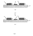
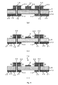
- Figure 1 exemplarily shows a part of the printed wiring board as a cross-sectional schematic view.
- first circuit and the “second circuit” will be described.
- the terms “first circuit” and “second circuit” referred to in this specification are used for the sake of convenience, in order to represent that thicknesses (cross-sectional areas) of the circuits are different.
- the first circuit with larger cross-sectional area than the cross-sectional area of the second circuit can be used as the power supply circuit or the like, while the second circuit having smaller cross-sectional area can be used as the signal transmission circuit.
- the first circuit and the second circuit which are distinguished in the present invention, simply mean a thicker circuit (circuit having large cross-sectional area) and a thinner circuit (circuit having small cross-sectional area) in respect of circuit thicknesses, and they do not mean extent of circuit widths. Also, they do not mean that all of the first circuits have the same circuit width and all of the second circuits have the same circuit width.
- the "same reference plane” means a planar surface or interface of an insulating layer which is formed by a base material such as glass-epoxy pre-preg or glass-polyimide pre-preg used in manufacturing the printed wiring board.
- the first circuit and the second circuit formed in the same reference plane means that the first and second circuits are placed to contact to the same reference plane when observing the printed wiring board from its cross section.
- both of the first circuit and the second circuit are disposed on one side of the same reference plane and (II) the first circuit is disposed on one side of the same reference plane and the second circuit is disposed on the oposite side.
- one of the first circuit and the second circuit is disposed to project from the printed wiring board surface, and the other circuit is buried in the printed wiring board surface.
- the projecting circuit is made to be thick as in Figure 1(1c) to use as the power supply circuit or the like, so that the circuit has a structure similar to a heat sink and thus heat sprezding effect is enhanced.
- the signal transmission circuit which is easily damaged by external force because the circuit is thin, is buried in the insulating layer, so that unexpected open circuit or the like can be prevented.
- the thickness of a thicker circuit of the first circuit and the second circuit is T 1 ⁇ m
- thickness T 2 of the other circuit is T 1 /100 to T 1 ( ⁇ m).
- the thinner circuit has thickness in a range of 5 ⁇ m to 500 ⁇ m.
- the thicknesses of the first circuit and the second circuit are appropriately optimally designed depending on supply current amount and there is no particular limitation on them. Therefore, the thickness of one of the circuits has a certain range in this description. In the present invention, as long as thicknesses of the first circuit and the second circuit are different, it is not particularly significant how much difference the thicknesses have.
- the printed wiring board is which is characterized in that the thicker circuit of the first circuit or the second circuit has a clad-like configuration in which three layers of a first copper layer/a different kind of metal layer/a second copper layer are sequentially stacked and nickel, tin, aluminum, titanium, or their alloy is used for the different kind of metal layer.
- the printed wiring board according to the present invention is a clad composite material in which three layers of a first copper layer/a different kind of metal layer/a second copper layer are sequentially stacked and nickel, tin, aluminum, titanium, or their alloy is used for the different kind of metal layer, so that efficient production can be achieved.
- a metal component used for the different kind of metal layer can be selectively etched against to copper.
- an etching solution used in this process is referred to as a "different kind of metal selective etching solution”.
- an etching solution in this process is referred to as a "copper selective etching solution”.
- a clad composite material in which three layers of a first copper layer/a different kind of metal layer/a second copper layer are sequentially stacked and aluminum or aluminum alloy (hereinafter simply referred to as a "aluminum base component") having the thickness of 50% to 80% of the total thickness of the clad composite material is used for the different kind of metal layer.
- aluminum base component aluminum or aluminum alloy
- the printed wiring board in order to achieve substantial weight reduction of the printed wiring board, it is required to replace at least 50% or more of the total thickness of the clad composite material by the aluminum base component.
- the thickness of the copper layer becomes insufficient due to the thickness in which the aluminum base component occupies, so that increase in resistance is extreme when the power supply circuit or the like is manufactured.
- the meaning of the product in which the power supply circuit or the like and the signal transmission circuit coexist in the same reference plane is lost.
- Method (1) for manufacturing single-sided or double-sided printed wiring board a method for manufacturing a so-called single-sided printed wiring board and a method for manufacturing a so-called double-sided printed wiring board have no difference in the basic processes, only having a difference whether a metal-clad laminate having a two-layer structure of a metal layer/an insulating layer is used or a metal-clad laminate having a three-layer structure of a first metal layer/an insulating layer/a second metal layer is used (here, it is assumed that the same material is used for the first metal layer and the second metal layer. However, it is not necessary that thicknesses of the first metal layer and the second metal layer are same).
- a method employed in this specification is a method for manufacturing a single-sided or a double-sided printed wiring board in which a first circuit and a second circuit having different thicknesses coexist in a same reference plane, characterized by comprising the following step 1-a to step 1-e.
- the forming step of a pass for interlayer connection is provided between the step 1-a and the step 1-b.
- the clad composite material in which an bonding surface to the base material is subjected to bond enhansing treatment for improving adhesion to the base material is used.
- Method (2) for manufacturing single-sided or double-sided printed wiring board may be a method for manufacturing a single-sided or double-sided printed wiring board in which a first circuit and a second circuit having different thicknesses coexist in a same reference plane and one circuit is buried in an insulating layer, characterized by comprising the following step 2-a to step 2-d.
- the forming step of a pass for interlayer connection is provided between the step 2-b and the step 2-c.
- the clad composite material with circuit pattern in which the different kind of metal layer exposed on the etched circuit pattern surface is removed.
- the clad composite material with circuit pattern in which the etched circuit pattern surface is subjected to bond enhansing treatment for improving adhesion to the base material.
- Method (3) for manufacturing single-sided or double-sided printed wiring board further, a method for manufacturing a single-sided or double-sided printed wiring board in which a first circuit or a second circuit having different thicknesses coexist in a same reference plane and one circuit is buried in an insulating layer, characterized by comprising the following step 3-a to step 3-c.
- this is a manufacturing method which can be performed only when a clad composite material with circuit pattern is used in which a different kind of metal layer exposed on an etched circuit pattern surface is removed.
- the forming step of a pass for interlayer connection is provided between the step 3-b and the step 3-c.
- the clad composite material with circuit pattern in which the etched circuit pattern surface is subjected to bond enhansing treatment for improving adhesion to the base material.
- Method (1) for manufacturing double-sided printed wiring board a method for manufacturing a double-sided printed wiring board referred to here is a method for manufacturing a double-sided printed wiring board in which a first circuit and a second circuit having different thicknesses coexist in a same reference plane on one surface side, characterized by comprising the following step 4-a to step 4-e.
- the forming step of a pass for interlayer connection is provided between the step 4-a and the step 4-b.
- an bonding surface of the clad composite material used here to the base material is subjected to bond enhansing treatment for improving adhesion to the base material.
- Method (2) for manufacturing double-sided printed wiring board a method for manufacturing a double-sided printed wiring board referred to here is also a method for manufacturing a double-sided printed wiring board in which a first circuit and a second circuit having different thicknesses coexist in a same reference plane on one surface side, characterized by comprising the following step 5-a to step 5-d.
- the forming step of a pass for interlayer connection is provided between the step 5-b and the step 5-c.
- the clad composite material with circuit pattern in which the different kind of metal layer exposed on the etched circuit pattern surface is removed.
- the clad composite material with circuit pattern in which the etched circuit pattern surface is subjected to bond enhansing treatment for improving adhesion to the base material.
- Method (1) for manufacturing multilayer printed wiring board in a method for manufacturing a so-called multilayer printed wiring board, an inner layer core material is included in an insulating layer in the case of manufacturing a double-sided printed wiring board. Therefore, this method is a method for manufacturing a printed wiring board comprising a circuit layer in which a first circuit and a second circuit having different thicknesses coexist in a same reference plane of an insulating layer located on a surface of an inner layer core material comprising an inner layer circuit, characterized by comprising the following step 6-a to step 6-e.
- the forming step of a pass for interlayer connection is provided between the step 6-a and the step 6-b in which through holes, via holes, or the like are formed for assuring electrical connection between the clad composite material and the inner layer circuit located on both surfaces of the insulating layer of the metal-clad laminate.
- an bonding surface of the clad composite material used here to the base material is subjected to bond enhansing treatment for improving adhesion to the base material.
- Method (2) for manufacturing a multilayer printed wiring board another method for manufacturing a multilayer printed wiring board is a method for manufacturing a printed wiring board comprising a circuit layer in which a first circuit and a second circuit having different thicknesses coexist in a same reference plane of an insulating layer located on a surface of an inner layer core material comprising an inner layer circuit, characterized by comprising the following step 7-a to step 7-d.
- the forming step of a pass for interlayer connection is provided between the step 7-b and the step 7-c in which through holes, via holes, or the like are formed for assuring electrical connection between the clad composite material with circuit pattern and the inner layer circuit located on both surfaces of the insulating layer of the metal-clad laminate.
- the clad composite material with circuit pattern in which the different kind of metal layer exposed on the etched circuit pattern surface is removed.
- the clad composite material with circuit pattern in which the etched circuit pattern surface is subjected to bond enhansing treatment for improving adhesion to the base material.
- the clad composite material having a configuration of the first copper layer/the different kind of metal layer/the second copper layer in which total thickness is 10 ⁇ m to 2000 ⁇ m and the thickness of the different kind of metal layer is 0.01 ⁇ m to 5 ⁇ m.
- the clad composite material having a configuration of the first copper layer/the different kind of metal layer/the second copper layer in which the total thickness of the three layers is 10 ⁇ m to 2000 ⁇ m, sum of the thickness of the first copper layer and the second copper layer is 1 ⁇ m to 1600 ⁇ m, and the different kind of metal layer has the thickness of 50% to 80% of the total thickness of the clad composite material and is constituted from a metal material which can be selectively etched against to copper. Further, by using aluminum base component lighter than copper for the different kind of metal layer, a lightweight printed wiring board can be manufactured.
- aluminum base component having the thickness of 50% to 80% of the total thickness of the clad composite material.
- the total thickness of the clad composite material is 10 ⁇ m to 2000 ⁇ m, it is more preferable that sum of the thickness of the first copper layer and the second copper layer is 5 ⁇ m to 1600 ⁇ m.
- a printed wiring board in the parts where sufficient circuit cross-sectional area must be assured, the thickness of the conductor can be increased for this purpose, so that substantial reduction in area of the substrate can be achieved.
- a printed wiring board is obtained in which the circuits having different electrical characteristics and usages are formed on a same reference plane.
- the projecting circuit parts of the printed wiring board can perform function in the same manner as heat sinks, so as to utilize them as circuits for heat spreader or heat spreading plates.
- a clad composite material which comprises a different kind of metal layer which can be selectively etched against to copper between two copper layers is used, so that efficient production of the printed wiring board according to the present invention can be achieved by using conventional lamination techniques of printed wiring boards, etching methods and apparatuses.
- a clad composite material is a start material and a so-called single-sided printed wiring board or so-called double-sided printed wiring board is manufactured.
- a method employed in this specification is a method for manufacturing a single-sided or double-sided printed wiring board comprising a circuit layer in which a first circuit and a second circuit having different thicknesses coexist in a same reference plane, characterized by comprising the following step 1-a to step 1-e.
- step 1-a to step 1-e Each step will be separately described below.
- Figure 2 to Figure 4 are referred to for the single-sided printed wiring board and Figure 5 to Figure 7 are referred to for the double-sided printed wiring board.
- Step 1-a in this step, a clad composite material in which three layers of a first copper layer/a different kind of metal layer/a second copper layer are sequentially stacked is used.
- the different kind of metal layer is constituted from a metal component which can be selectively etched against to copper.
- This step is a laminating step in which, as shown in Figure 2(a), the clad composite material 2 (the first copper layer 3, the different kind of metal layer 4, the second copper layer 5) is bonded to a base material 6 constituting an insulating layer (such as a pre-preg formed by impregnating and drying epoxy resin or the like in a skeletal material such as glass fabric or aramid fabric, or a polyimide resin film) to form a metal-clad laminate 7 in Figure 2(b).
- an insulating layer such as a pre-preg formed by impregnating and drying epoxy resin or the like in a skeletal material such as glass fabric or aramid fabric, or a polyimide resin film
- an bonding surface of the clad composite material 2 to the base material 6 is previously subjected to bond enhansing treatment in order to improve adhesion to the base material, so that generation of faults such as delamination and measling due to heat shock after forming the printed wiring board can be efficiently prevented.
- the bond enhansing treatment referred to here is typified by so-called black oxide treatment (including reduction black oxide treatment which is made in consideration of pink-ring resistivity).
- black oxide treatment a method of roughening the copper surface with a sulfuric acid-hydrogen peroxide base microetching agent (for example, MEC Etch Bond manufactured by MEC Co., Ltd.) or depositing fine copper particles by burning plating of copper can be employed, for example.
- the "bond enhansing treatment” means these treatments.
- the clad composite materials 2 are bonded to both surfaces of the base material 6 constituting the insulating layer to form a double-sided metal-clad laminate 7' in Figure 5(b). Also in the case of manufacturing the double-sided printed wiring board, the contact surface of the clad composite material 2 to the base material 6 can be previously subjected to the bond enhansing treatment.
- the clad composite material it is preferable to use, as the clad composite material, (i) a material made by sequentially laminated to unite a copper foil, a different kind of metal foil, and a copper foil or (ii) a material made by providing a different kind of metal layer on one surface of one sheet of copper layer, laying another copper foil over the different kind of metal layer, and then unite them by rolling.
- Such a clad composite material can be also manufactured by electrolysis, it is impossible to directly electrodeposit copper to a surface of aluminum or aluminum alloy if aluminum or aluminum alloy is used as the different kind of metal layer. Therefore, by using rolling, the layers can be united more easily and thickness control of the different kind of metal layer is also easier, if rolling is used. Further, while deposition defect or the like may be generated if the different kind of metal layer is formed on the copper layer by electrolysis, defect extinction and uniformity of film thickness in the different kind of metal layer are dramatically enhanced by once rolling.
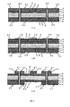
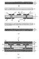
- interlayer connection pass forming In the case of the double-sided metal-clad laminate 7' shown in Figure 5(b), in order to assure electrical connection between the clad composite materials which are conductor layers on both surfaces, through holes or via holes 22 are formed and plating treatment is performed in the holes to assure electrical connection between the layers, as shown in Figure 6(c). In this specification, this is referred to as interlayer connection pass forming. If plating is employed here, plating layers 23 are formed by catalyzing, electroless copper plating, and electroplating. Thus, generally, the plating layers 23 are formed also on the surfaces of the first copper layers on the outer layers. However, this interlayer connection pass forming is not an indispensable step and may be unnecessary depending on board designs. The same applies in the following description.
- etching resists 10 are provided on surfaces of the plating layers 23 in the strict sense, the expression "etching resists 10 are provided on the first copper layers 3" or the like may be used for convenience of explanation, as long as those skilled in the art can understand.
- Step 1-b in this first copper etching step, as shown in Figure 2(c), the etching resist layer 10 is formed on the first copper layer 3 located on the outer layer of the metal-clad laminate, and a circuit pattern for etching is exposed and developed to etch the first copper layer 3 located on the outer layer into a desired circuit pattern (temporary circuits 21) with a copper selective etching solution, and then etching resist releasing is performed to remove unnecessary first copper layer, form the temporary circuits 21, and expose the different kind of metal layer 4, as in Figure 3(d).
- a desired circuit pattern temporary circuits 21
- etching resist releasing is performed to remove unnecessary first copper layer, form the temporary circuits 21, and expose the different kind of metal layer 4, as in Figure 3(d).
- the copper selective etching solution referred to here is a solution which is used to dissolve only copper without dissolving the different kind of metal, and it is most convenient and preferable to use ammonia base alkaline etching solution. The same applies in the following description, for the copper selective etching solution.
- all intermediate circuit shapes before the final circuit shape are referred to as the "temporary circuits 21" for explanation.
- the etching resist layers 10 are formed on the first copper layers 3 after the interlayer connection pass forming, and circuit patterns for etching are exposed and developed to etch the first copper layers 3 located on the outer layers into desired circuit patterns with the copper selective etching solution, and then etching resist releasing is performed to remove unnecessary first copper layers, form the temporary circuits 21, and expose the different kind of metal layers 4, as in Figure 6(e).
- Step 1-c in this first different kind of metal etching step, after the first copper etching step is finished, the different kind of metal layer exposed between the temporary circuits 21 formed on the outer layer is etched away with a different kind of metal selective etching solution, as shown in Figure 3(e).
- This step is the same also in the case of manufacturing the double-sided printed wiring board.
- the different kind of metal layers exposed between the circuits temporarily formed on the outer layers as shown in Figure 6(e) are etched away with the different kind of metal selective etching solution, as shown in Figure 7(f).
- etching solutions which are appropriately prepared depending on the type of the different kind of metal.
- a chlorine base or sulfuric acid base acid etching solution is used for the different kind of metal of nickel base metal component
- an acid etching solution is used for the different kind of metal of tin base metal component
- an alkaline base etching solution is used for the different kind of metal of aluminum base metal component.
- Step 1-d in this second copper etching step, after the first different kind of metal etching step is finished, as shown in Figure 3(f), the etching resist layer 10 is again formed only on area which is to be the first circuit, and etching is performed with the copper selective etching solution to etch away area of the first copper layer where no etching resist layer 10 is present, so that the shapes of the first circuits 8 are finished and the second circuit 9 still having the different kind of metal layer is formed, and then etching resist releasing is performed to expose the different kind of metal layer 4 of the second circuit 9.
- This step is the same also in the case of the double-sided printed wiring board.
- the etching resist layers 10 are again formed only on area which is to be the first circuit, and etching is performed with the copper selective etching solution to etch away area of the first copper layers where no etching resist layer 10 is present, so that the shape of the first circuit 8 is finished and the second circuit 9 still having the different kind of metal layer 4 is formed, and then etching resist releasing is performed to expose the different kind of metal layer 4 of the second circuit 9.
- Step 1-e further, in the second different kind of metal etching step, only the different kind of metal layer on the surface of the second circuit is removed with the different kind of metal selective etching solution to form the final shape of the second circuit 9, so that a printed wiring board 1a as shown in Figure 4(h) is obtained.
- This step is the same also in the case of manufacturing the double-sided printed wiring board. Only the different kind of metal layer on the surface of the second circuit is removed with the different kind of metal selective etching solution to form the final shape of the second circuit 9, so that a printed wiring board 1b as shown in Figure 7(h) is obtained.
- a clad composite material is a start material and single-sided printed wiring board or a so-called double-sided printed wiring board is manufactured.
- a method employed in this specification is a method for manufacturing a single-sided or double-sided printed wiring board comprising a circuit layer in which a first circuit and a second circuit having different thicknesses coexist in a same reference plane, and one circuit is buried in an insulating layer, the method characterized by comprising the following step 1-a to step 1-d.
- step 1-a to step 1-d Each step will be separately described below.
- Figure 8 to Figure 10 are referred to for the single-sided printed wiring board and Figure 13 to Figure 15 are referred to for the double-sided printed wiring board.
- Step 2-a in this manufacturing process step, at first, in a clad composite material etching step, a clad composite material in which three layers of a first copper layer/a different kind of metal layer/a second copper layer are sequentially stacked has the different kind of metal layer constituted from a metal component which can be selectively etched against to copper.
- this clad composite material 2 only the second copper layer is etched with a copper selective etching solution to form a circuit pattern for etching on one surface, so that a first clad composite material with circuit pattern 11 shown in Figure 8(c) is obtained.
- the first clad composite material with circuit pattern 11 is obtained by forming etching resist layers 10 on both surfaces of the clad composite material 2, exposing and developing a circuit pattern for etching for forming temporary circuits 21 only on the etching resist layer of the second copper layer as shown Figure 8(b), etching the second copper layer 5 located on the outer layer into a desired circuit pattern with the copper selective etching solution, and then performing etching resist releasing.
- the etched circuit pattern surfaces of the clad composite material with a first circuit pattern 11 and the clad composite material with a second circuit pattern 11' are previously subjected to bond enhansing treatment in order to improve adhesion to the base material, so as to efficiently prevent generation of faults such as delamination and measling due to heat shock after forming the printed wiring board.
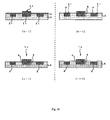
- Step 2-b a laminating step will be described. If the clad composite material with a first circuit pattern 11 is used, as shown in Figure 9(e-I), the etched circuit pattern surface of the clad composite material with a first circuit pattern 11 obtained in the clad composite material etching step, on which the temporary circuits 21 are formed, is placed onto a surface of the base material 6 and bonded to the base material surface to form a metal-clad laminate 7 in which the etched pattern is buried in the insulating layer, as shown in Figure 9 (f-I) .
- the etched circuit pattern surface of the clad composite material with a second circuit pattern 11' obtained in the clad composite material etching step, on which the temporary circuits 21 are formed is placed onto a surface of the base material 6 and bonded to the base material surface to form a metal-clad laminate 7 in which the etched pattern is buried in the insulating layer, as shown in Figure 9(f-II).
- a difference from the case of using the clad composite material with a first circuit pattern 11 is that the different kind of metal layer 4 between the temporary circuits 21 and the first copper layer is also buried in the base material 6.
- the clad composite material 2 shown in Figure 13(a) is a start material, and two first clad composite material with circuit patterns 11 shown in Figure 13(b) are used and their etched circuit pattern surfaces on which the temporary circuits 21 are formed are bonded to both surfaces of the base material 6 constituting the insulating layer as shown in Figure 13(c), to form a double-sided metal-clad laminate 7' in which temporary circuits 21 are buried in the insulating layer 6 as in Figure 14(d).
- the manufacturing process of the double-sided printed wiring board will be exemplarily described for the case where the clad composite material with a first circuit pattern 11 is used.
- the clad composite material with a first circuit pattern 11 instead of the clad composite material with a first circuit pattern 11, the clad composite material with a second circuit pattern 11' may be used, and the etched circuit pattern surfaces of the clad composite material with a first circuit pattern 11 and the clad composite material with a second circuit pattern 11' can be previously subjected to the bond enhansing treatment, as required.
- the clad composite material referred to here is the same as described above.
- a through holes or via hole 22 is formed and plating treatment is performed in the hole to assure electrical connection between the layers, as shown in Figure 14(e).
- the description of this interlayer connection pass forming will be omitted because it is the same as described above, in order to avoid repetition.
- Step 2-c in this first copper etching step, as shown in Figure 9(g-I) for the case of using the clad composite material with a first circuit pattern 11, and as shown in Figure 9(g-II) for the case of using the clad composite material with a second circuit pattern 11', the etching resist layer 10 is formed on the first copper layer 3 on the outer layer surface of the metal-clad laminate 7, and a circuit pattern for etching is exposed and developed to etch the first copper layer 3 located on the outer layer into a desired circuit pattern with a copper selective etching solution, and then etching resist releasing is performed.
- the etching resist layers 10 are formed on the first copper layers 3 on the outer layer surfaces of the metal-clad laminate 7, and circuit pattern for etching is exposed and developed to etch the first copper layers 3 located on the outer layers into desired circuit patterns with the copper selective etching solution, and then etching resist releasing is performed to remove unnecessary first copper layers 3, form the temporary circuits 21, and expose parts of the different kind of metal layers 4, as in Figure 15(g).
- Step 2-d in this different kind of metal etching step, after the first copper etching step is finished, the different kind of metal layer is etched away with a different kind of metal selective etching solution to form the first circuit and the second circuit. Therefore, in the case of using the clad composite material with a first circuit pattern 11, a printed wiring board 1c as shown in Figure 10 (i-I) is obtained. On the other hand, in the case of using the clad composite material with a second circuit pattern 11', a printed wiring board 1c as shown in Figure 10(i-II) is obtained.
- the different kind of metal layers are etched away with the different kind of metal selective etching solution to form the first circuits and the second circuits, so that a printed wiring board 1d as shown in Figure 15(h) is obtained.
- a clad composite material is a start material and a so-called single-sided printed wiring board or a so-called double-sided printed wiring board is manufactured.
- a method employed in this specification is a method for manufacturing a single-sided or double-sided printed wiring board comprising a circuit layer in which a first circuit and a second circuit having different thicknesses coexist in a same reference plane, and one circuit is buried in the insulating layer, the method characterized by comprising the following step 3-a to step 3-c.
- step 3-a to step 3-c Each step will be separately described below.
- Figure 11 to Figure 12 are referred to for the single-sided printed wiring board, and illustration of the double-sided printed wiring board will be omitted.
- Step 3-a in this manufacturing process step, at first, in a clad composite material etching step, a clad composite material in which three layers of a first copper layer/a different kind of metal layer/a second copper layer are sequentially stacked has the different kind of metal layer constituted from a metal component which can be selectively etched against to copper.
- this clad composite material 2 only the second copper layer is etched with a copper selective etching solution to form a circuit pattern for etching on one surface, so that the clad composite material with a first circuit pattern 11 shown in Figure 8(c) is obtained.
- the etched circuit pattern surface of the clad composite material with a second circuit pattern 11' is previously subjected to bond enhansing treatment in order to improve adhesion to the base material, so as to efficiently prevent generation of faults such as delamination and measling due to heat shock after forming the printed wiring board.
- Step 3-b a laminating step will be described.
- the clad composite material with a second circuit pattern 11' shown in Figure 11(a) is used and the etched circuit pattern surface of the clad composite material with a second circuit pattern 11' obtained in the clad composite material etching step, on which the temporary circuits 21 are formed, is placed onto a surface of the base material 6 and bonded to the base material surface as shown in Figure 11 (b), to form a metal-clad laminate 7 in which the etched pattern is buried in the insulating layer, as shown in Figure 11(c).
- double-sided printed wiring board is manufactured, in this laminating step, two second clad composite material with circuit pattern 11' shown in Figure 11(a) are used and their etched circuit pattern surfaces on which the temporary circuits 21 are formed are bonded to both surfaces of the base material 6 constituting the insulating layer as shown in Figure 11(b), to form a double-sided metal-clad laminate. Illustration of the manufacturing process of the double-sided printed wiring board will be omitted.
- interlayer connection pass for assuring electrical connection between the layers can be formed, such as through holes or via holes. The description for them will be omitted because it is the same as described above, in order to avoid repetition.
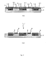
- Step 3-c in this first copper etching step, as shown in Figure 12(d), the etching resist layer 10 is formed on the first copper layer 3 on the outer layer surface of the metal-clad laminate 7, and a circuit pattern for etching is exposed and developed to etch the first copper layer 3 located on the outer layer into a desired circuit pattern with a copper selective etching solution, and then etching resist releasing is performed.
- a circuit pattern for etching is exposed and developed to etch the first copper layer 3 located on the outer layer into a desired circuit pattern with a copper selective etching solution, and then etching resist releasing is performed.
- the clad composite material with a second circuit pattern 11' remaining parts of the second copper layer which have been previously etched form the first circuit 8, and area having only the first copper layer is etched to form the thin second circuit 9, so that a printed wiring board 1c' is obtained.
- the subsequent different kind of metal etching of the different kind of metal layer is eliminated.
- a clad composite material is a start material and a so-called double-sided printed wiring board is manufactured.
- a first circuit and a second circuit having different thicknesses coexist only in a same reference plane on one surface side of the double-sided printed wiring board, and the process step is characterized by comprising the following step 4-a to step 4-e.
- Figure 16 to Figure 18 are referred to in the following description.
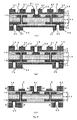
- Step 4-a in this laminating step, as shown in Figure 16(a), the above described clad composite material 2 and a conventional copper foil 12 are laminated and bonded to respective one surface side of a base material constituting an insulating layer to form a double-sided metal-clad laminate 7' shown in Figure 16 (b) .
- through holes or via holes 22 are formed for assuring electrical connection between the clad composite material 2 and the copper foil 12 located on both surfaces of the insulating layer of the double-sided metal-clad laminate 7'. This forming method is the same as described above and the description is not repeated here.
- the bonding surface of the clad composite material 2 to the base material 6 is previously subjected to bond enhansing treatment in order to improve adhesion to the base material, so that generation of faults such as delamination and measling due to heat shock after forming the printed wiring board can be efficiently prevented.
- the bond enhansing treatment referred to here is the same as described above.
- Step 4-b in this first copper etching step, as shown in Figure 17(d), etching resist layers 10 are formed on the first copper layer 3 of the clad composite material 2 located on one surface side of the insulating layer and on the copper foil layer 12 on the other surface side, and circuit pattern for etching is exposed and developed to etch the first copper layer 3 and the copper foil 12 located on the outer layers into desired circuit patterns with a copper selective etching solution, and then etching resist releasing is performed to remove unnecessary first copper layer 3, form the temporary circuits 21, and expose the different kind of metal layer 4 between the temporary circuits 21, and form the copper foil 12 into a desired circuit pattern, as shown in Figure 17(e).
- Step 4-c in this first different kind of metal etching step, after the first copper etching step is finished, the different kind of metal layer 4 exposed between the temporary circuits 21 formed on the outer layer is etched away with a different kind of metal selective etching solution, as shown in Figure 17 (f).
- Step 4-d in this second copper etching step, after the first different kind of metal etching step is finished, as shown in Figure 18(g), the etching resist layers 10 are again formed only on area which is to be the first circuit and on the circuit formed by etching the copper foil layer, and etching is performed with the copper selective etching solution to etch away area of the first copper layer where no etching resist layer is present, and then etching resist releasing is performed to form the first circuit and the second circuit still having the different kind of metal layer, as shown in Figure 18(h).
- Step 4-e in this second different kind of metal etching step, only the different kind of metal layer on the surface of the second circuit is removed with the different kind of metal selective etching solution to form the second circuit shape, so that a printed wiring board 1e is obtained as shown in Figure 18 (i) .
- a clad composite material is a start material and a so-called double-sided printed wiring board is manufactured.
- a first circuit and a second circuit having different thicknesses coexist only in a same reference plane on one surface side of the double-sided printed wiring board, and one of the first circuit and the second circuit is buried in an insulating layer, and the process step is characterized by comprising the following step 5-a to step 5-d.
- Figure 19 to Figure 21 are referred to in the following description.
- Step 5-a this clad composite material etching step is the same as described above, in which the clad composite material 2 shown in Figure 19(a) is a start material and the clad composite material with a first circuit pattern 11 shown in Figure 19(b) is manufactured by the process shown in Figure 8. Also in this manufacturing process step, the clad composite material with a second circuit pattern 11' shown in Figure 8(d) may be used.
- the difference for the following steps between the case of using the clad composite material with a first circuit pattern 11 and the case of using the clad composite material with a second circuit pattern 11' is the difference shown in Figure 9 and Figure 10 in a comparative manner, which can be easily understood by those skilled in the art.
- the following steps will be described only with the clad composite material with a first circuit pattern 11. Therefore, the clad composite material is simply referred to as a "clad composite material with circuit pattern 11".
- the bonding surface of the clad composite material with circuit pattern 11, 11' to the base material 6 is previously subjected to bond enhansing treatment in order to improve adhesion to the base material, so that generation of faults such as delamination and measling due to heat shock after forming the printed wiring board can be efficiently prevented.
- the bond enhansing treatment referred to here is the same as described above.
- Step 5-b in this laminating step, the clad composite material with circuit pattern 11 and the copper foil 12 are used and laminated as shown in Figure 19(c) and bonded to respective surfaces of the base material constituting the insulating layer to form a double-sided metal-clad laminate 7' as shown in Figure 20(d).
- a through hole or via hole 22 is formed for assuring electrical connection between the clad composite material with circuit pattern 11 and the copper foil 12 located on both surfaces of the insulating layer 6 of the double-sided metal-clad laminate 7'.
- This forming method is the same as described above and the description is not repeated here.
- Step 5-c in the first copper etching step, etching resist layers 10 are formed on the first copper layer of the clad composite material located on one surface side of the insulating layer and on the copper foil layer on the other surface side, and circuit pattern for etching is exposed and developed as shown in Figure 20(f) to etch the first copper layer and the copper foil located on the outer layers into desired circuit patterns with a copper selective etching solution, and then etching resist releasing is performed to expose the different kind of metal layer 4 as shown in Figure 21 (g).
- Step 5-d in this first different kind of metal etching step, after the first copper etching step is finished, the different kind of metal layer 4 exposed between the circuits temporarily formed on the outer layer is etched away with a different kind of metal selective etching solution to form the first circuit 8, the second circuit 9, and a copper foil circuit 13, so that a printed wiring board 1f is obtained as shown in Figure 21(h).
- the manufacturing flow of the multilayer printed wiring board is basically the same as the manufacturing flow of the double-sided printed wiring board and therefore it is considered that explicit description is less necessary. This is because it is only required to replace the base material 6 used in manufacturing the double-sided metal-clad laminate described above by an "inner layer core material" and "base materials disposed on both surfaces of the inner layer core material".
- the manufacturing process steps of the multilayer printed wiring board will be described below.
- a manufacturing process step of a multilayer printed wiring board which comprises a circuit layer in which a first circuit and a second circuit having different thicknesses coexist in a same reference plane of an insulating layer located on a surface of an inner layer core material comprising an inner layer circuit.
- the method for manufacturing the multilayer printed wiring board referred to here is characterized by comprising the following step 6-a to step 6-e.
- Figure 22 to Figure 25 are referred to in the following description.
- Step 6-a in this laminating step, the clad composite material is laminated on one surface or both surfaces of the inner layer core material via an insulating layer constituting material such as a pre-preg to form a multilayer metal-clad laminate.
- Figure 22(a) shows a laminating image in the case where clad composite materials 2 are bonded to an inner layer core material 14 on both surfaces via base materials constituting insulating layers 6. Then, hot pressing is performed to form a multilayer metal-clad laminate 7" shown in Figure 22(b).
- the inner layer core material 14 comprises inner layer circuits 15 and has via holes in this illustration, there is no particular limitation on the type of the inner layer core material and a various materials can be used such as a so-called rigid substrate or flexible substrate.
- Step 6-b in this first copper etching step, as shown in Figure 23(d), the etching resist layers 10 are formed on the first copper layers 3 located on the outer layers of the multilayer metal-clad laminate 7", and circuit pattern for etching is exposed and developed to etch the first copper layers located on the outer layers into desired circuit patterns with a copper selective etching solution, and then etching resist releasing is performed to form the temporary circuits 21 and expose the different kind of metal layers 4, in area where unnecessary first copper layers is removed, as shown in Figure 23(e).
- Step 6-c in this first different kind of metal etching step, after the first copper etching step is finished, the different kind of metal layers 4 exposed between the temporary circuits 21 formed on the outer layers are etched away with a different kind of metal selective etching solution, as shown in Figure 23(f).
- Step 6-d in this second copper etching step, after the first different kind of metal etching step is finished, as shown in Figure 24(g), the etching resist layers 10 are again formed only on area which is to be the first circuit, and etching is performed with the copper selective etching solution to etch away area of the first copper layer where no etching resist layer 10 is present, and then etching resist releasing is performed to form the first circuits 8 and the second circuit still having the different kind of metal layer 4, as shown in Figure 24(h).
- Step 6-e in this second different kind of metal etching step, only the different kind of metal layer 4 on the surface of the second circuit is removed with the different kind of metal selective etching solution to form the shape of the second circuit 9, so that a multilayer printed wiring board 1g is obtained as shown in Figure 25 (i) .
- a manufacturing process step of a multilayer printed wiring board in which a first circuit and a second circuit having different thicknesses coexist in a same reference plane of an insulating layer located on a surface of an inner layer core material comprising an inner layer circuit and one of the circuits is buried in the insulating layer.
- the method for manufacturing the multilayer printed wiring board referred to here is characterized by comprising the following step 7-a to step 7-d.
- Figure 26 to Figure 28 are referred to in the following description.
- Step 7-a this clad composite material etching step is the same as described above and it is a step of manufacturing a clad composite material with circuit pattern 11 in which clad composite materials 2 shown in Figure 26(a) comprise the temporary circuits 21 by the process shown in Figure 8. Therefore, the description will be omitted here.
- the clad composite material with a second circuit pattern 11' shown in Figure 8(d) may be used.
- the difference for the following steps between the case of using the clad composite material with a first circuit pattern 11 and the case of using the clad composite material with a second circuit pattern 11' is the difference shown in Figure 9 and Figure 10 in a comparative manner, which can be easily understood by those skilled in the art.
- the following steps will be described only with the clad composite material with a first circuit pattern 11. Therefore, the clad composite material is simply referred to as a "clad composite material with circuit pattern 11".
- the bonding surface of the clad composite material with circuit pattern 11, 11' to the base material 6 is previously subjected to bond enhansing treatment in order to improve adhesion to the base material, so that generation of faults such as delamination and measling due to heat shock after forming the printed wiring board can be efficiently prevented.
- the bond enhansing treatment referred to here is the same as described above.
- Step 7-b in this laminating step, the etched circuit pattern surface of the clad composite material with circuit pattern 11 is placed onto a base material surface and laminated on one surface or both surfaces of the inner layer core material via an insulating layer constituting material such as pre-preg, to form a multilayer metal-clad laminate.
- Figure 26(a) shows a laminating image in the case where the clad composite material with circuit patterns 11 are bonded to an inner layer core material 14 on both surfaces via base materials constituting insulating layers 6. Then, hot pressing is performed to form a multilayer metal-clad laminate 7" in which the temporary circuits 21 on the etched circuit pattern surfaces of the clad composite material with circuit patterns 11 are buried in the insulating layers 6, as shown in Figure 26(b).
- the inner layer core material 14 referred to here also comprises inner layer circuits 15 and has via holes in this illustration, there is no particular limitation on the type of the inner layer core material and a various materials can be used such as a so-called rigid substrate or flexible substrate
- Step 7-c in this first copper etching step, as shown in Figure 27(d), the etching resist layers 10 are formed on the first copper layers 3 located on the outer layers of the multilayer metal-clad laminate 7", and circuit pattern for etching is exposed and developed to etch the first copper layers located on the outer layers into desired circuit patterns with a copper selective etching solution, and then etching resist releasing is performed to form the temporary circuits 21 and expose the different kind of metal layers 4, in area where unnecessary first copper layers is removed, as shown in Figure 28(e).
- Step 7-d in this first different kind of metal etching step, after the first copper etching step is finished, the different kind of metal layers 4 exposed between the temporary circuits 21 formed on the outer layers are etched away with a different kind of metal selective etching solution to simultaneously finish the first circuits 8 and the second circuits 9, so that a multilayer printed wiring board 1h is obtained as shown in Figure 28 (f).
- the printed wiring board according to the present invention in order to manufacture the printed wiring board according to the present invention, it is preferable to use one of nickel, tin, aluminum, titanium, and their alloy which can be selectively etched against to copper, for the different kind of metal layer. This has been already described above.
- the clad composite material it is preferable to use a configuration of a first copper layer/a different kind of metal layer/a second copper layer in which total thickness is 10 ⁇ m to 2000 ⁇ m and the thickness of the different kind of metal layer is 0.01 ⁇ m to 5 ⁇ m. If the thickness of the different kind of metal layer in this case is below 0.01 ⁇ m, the layer can not perform function as a barrier against a copper etching solution. On the other hand, if the thickness of the different kind of metal layer is above 5 ⁇ m, the layer can not be easily removed by etching.
- the clad composite material it is also preferable to use a configuration of a first copper layer/a different kind of metal layer/a second copper layer in which the total thickness of the three layers is 10 ⁇ m to 2000 ⁇ m, sum of the thickness of the first copper layer and the second copper layer is 1 ⁇ m to 1600 ⁇ m, and the different kind of metal layer has the thickness of 50% to 80% of the total thickness of the clad composite material and is constituted from a metal material which can be selectively etched against to copper.
- aluminum base component having the thickness of 50% to 80% of the total thickness of the clad composite material.
- the total thickness of the clad composite material is 10 ⁇ m to 2000 ⁇ m, it is more preferable that sum of the thickness of the first copper layer and the second copper layer is 5 ⁇ m to 1600 ⁇ m. In this way, a large amount of the component which is lighter than copper is used as the metal component constituting the conductor layer, so that total weight of the printed wiring board is reduced.
- the different kind of metal layer it is conceivable to employ aluminum or aluminum base alloy such as duralumin.
- molybdenum base alloy is also preferable as the alloy which is lighter than copper.
- the lower limit value of the thickness of the different kind of metal layer in this case is 50% of the total thickness of the clad composite material.
- this thickness is the minimal thickness for achieving weight reduction effect which can be clearly recognized, because the weight of the base material is present in the case of the printed wiring board.
- the thickness of the different kind of metal layer is above 80% of the total thickness of the clad composite material, the thickness of the conductor through which current flows actually is reduced, which can cause unexpected resistive heat generation.
- Step 1-a in this laminating step, a clad composite material 2 was used in which three layers of a first copper layer (80 ⁇ m)/a different kind of metal layer (1 ⁇ m nickel layer)/a second copper layer (80 ⁇ m) were sequentially stacked.
- the bonding surface of this clad composite material 2 to a base material was subjected to black oxide treatment as bond enhansing treatment, by means of a known approach.
- this clad composite material 2 (the first copper layer 3, the different kind of metal layer 4, the second copper layer 5) was bonded to a base material 6 (a FR-4 grade glass-epoxy pre-preg having the thickness of 210 ⁇ m) constituting an insulating layer by hot pressing with the order of 180°C 60 minutes, to form a metal-clad laminate 7 in Figure 2(b).
- the clad composite material used here was made by forming a nickel layer on one surface of one sheet of copper foil by plating, laying another copper foil over the nickel layer, and cladded them by rolling.
- Step 1-b in this first copper etching step, as shown in Figure 2(c), an etching resist layer 10 was formed with a dry film on the first copper layer 3 located on the outer layer of the metal-clad laminate 7, and a circuit pattern for etching was exposed and developed to etch the first copper layer 3 located on the outer layer into a desired circuit pattern (temporary circuits 21) with a copper selective etching solution (ammonia base alkaline copper etching solution: A-Process manufactured by Meltex Inc. The same applies in the following description). Thereafter, etching resist releasing by swelling with an alkaline solution was performed after removing unnecessary first copper layer, form the temporary circuits 21, and expose the different kind of metal layer 4, as in Figure 3(d).
- a copper selective etching solution ammonia base alkaline copper etching solution: A-Process manufactured by Meltex Inc. The same applies in the following description.
- Step 1-c in this first different kind of metal etching step, after the first copper etching step was finished, the different kind of metal layer 4 exposed between the temporary circuits 21 formed on the outer layer was etched away with a different kind of metal selective etching solution (nickel remover manufactured by MEC Co., Ltd.), as shown in Figure 3 (e).
- a different kind of metal selective etching solution nickel remover manufactured by MEC Co., Ltd.
- Step 1-d in this second copper etching step, after the first different kind of metal etching step was finished, as shown in Figure 3(f), the etching resist layer 10 was again formed with a liquid resist only on area which is to be the first circuit, and etching was performed with the copper selective etching solution (ammonia base alkaline copper etching solution) to etch away area where no etching resist layer 10 is present, so that the shape of the first circuit 8 was finished and a second circuit 9 still having the different kind of metal layer was formed, and then etching resist releasing was performed to expose the different kind of metal layer 4 of the second circuit 9.
- the copper selective etching solution ammonia base alkaline copper etching solution
- Step 1-e further, in the second different kind of metal etching step, only the different kind of metal layer 4 on the surface of the second circuit was removed with the different kind of metal selective etching solution (nickel remover manufactured by MEC Co., Ltd.) to form the final shape of the second circuit 9, so that the printed wiring board 1a shown in Figure 4(h) was obtained.
- Both the first circuit 8 and the second circuit 9 in this case project from the insulating layer surface, and the thickness of the first circuit is 161 ⁇ m and the thickness of the second circuit is 80 ⁇ m.
- the first circuit can be used as a power supply circuit or the like, so that heat accumulation in the insulating layer of the substrate can be prevented and heat can be efficiently spreaded to the surrounding atmosphere, even if heat generation is great.
- Step 1-a in this laminating step, a clad composite material 2 was used in which three layers of a first copper layer (80 ⁇ m)/a different kind of metal layer (1 ⁇ m nickel layer)/a second copper layer (80 ⁇ m) were sequentially stacked.
- the bonding surface of this clad composite material 2 to a base material was subjected to black oxide treatment as bond enhansing treatment, by means of a known approach.
- the clad composite materials 2 (the first copper layers 3, the different kind of metal layers 4, the second copper layers 5) were bonded to both surfaces of a base material 6 (a FR-4 grade glass-epoxy pre-preg having the thickness of 210 ⁇ m) constituting an insulating layer by hot pressing with the order of 180° C' 60 minutes, to form a metal-clad laminate 7' in Figure 5(b).
- the clad composite material used here was also made by providing a nickel layer on one surface of one sheet of copper foil by plating, laying another copper foil over the nickel layer, and cladded them by rolling, as in example 1.
- Step 1-b in this first copper etching step, as shown in Figure 6(d), etching resist layers 10 were formed with dry films on the first copper layers 3 after the interlayer connection pass forming, and circuit pattern for etching was exposed and developed to etch the first copper layers 3 located on the outer layers into desired circuit patterns with a copper selective etching solution (ammonia base alkaline etching solution). Thereafter, etching resist releasing by swelling with an alkaline solution was performed after removing unnecessary first copper layers, form the temporary circuits 21, and expose the different kind of metal layers 4, as in Figure 6(e).
- the copper selective etching solution described here was also used in the following steps.
- Step 1-c in this first different kind of metal etching step, after the first copper etching step was finished, the different kind of metal layers 4 exposed between the temporary circuits 21 formed on the outer layers were etched away with a different kind of metal selective etching solution (nickel remover manufactured by MEC Co., Ltd.), as shown in Figure 7(f).
- the nickel base different kind of metal selective etching solution described here was also used in the following steps.
- Step 1-d in the second copper etching step, after the first different kind of metal etching step was finished, as shown in Figure 7(g), the etching resist layers 10 were again formed with a liquid resist only on area which is to be the first circuit, and etching was performed with the copper selective etching solution to etch away area of first copper layers where no etching resist layer 10 is present, so that the shapes of the first circuits 8 were finished and the second circuit 9 still having the different kind of metal layer 4 was formed, and then etching resist releasing was performed to expose the different kind of metal layer 4 of the second circuit 9.
- Step 1-e further, in the second different kind of metal etching step, only different kind of metal layer 4 on the surface of the second circuit was removed with the different kind of metal selective etching solution to form the final shape of the second circuit 9, so that the double-sided printed wiring board 1b as shown in Figure 7(h) was obtained.
- Both the first circuits 8 and the second circuit 9 project from the insulating layer surface, and the thickness of the first circuit is 161 ⁇ m and the thickness of the second circuit is 80 ⁇ m.
- the first circuits can be used as circuits for power supply or the like, so that heat accumulation in the insulating layer of the substrate can be prevented and heat can be efficiently spreaded to the surrounding atmosphere, even if heat generation is great.
- a single-sided printed wiring board 1c shown in Figure 10(i-I) was manufactured.
- the single-sided printed wiring board comprises a circuit layer in which a first circuit and a second circuit having different thicknesses coexist in a same reference plane, and one circuit is buried in an insulating layer.
- Each step will be separately described below and Figure 8 to Figure 10 are referred to in the description.
- Step 2-a in this clad composite material etching step, a clad composite material 2 shown in Figure 8(a) was used in which three layers of a first copper layer (300 ⁇ m)/a different kind of metal layer (1 ⁇ m nickel layer)/a second copper layer (80 ⁇ m) were sequentially stacked.
- etching resist layers 10 were formed on both surfaces of the clad composite material 2 by laminating dry films, and a circuit pattern for etching for forming temporary circuits 21 was exposed and developed only on the etching resist layer of the second copper layer as shown in Figure 8(b) to etch the second copper layer 5 located on the outer layer into a desired circuit pattern with a copper selective etching solution (ammonia base alkaline copper etching solution), and then etching resist releasing was performed to obtain a first clad composite material with circuit pattern 11 shown in Figure 8(c).
- the bonding surface of the clad composite material with a first circuit pattern 11 to a base material was subjected to black oxide treatment as bond enhansing treatment, by means of a known approach.
- Step 2-b in this laminating step, as shown in Figure 9(e-I), the etched circuit pattern surface of the clad composite material with circuit pattern 11 obtained in the clad composite material etching step, on which the temporary circuits 21 were formed, was placed onto a surface of a base material 6 (a FR-4 grade glass-epoxy pre-preg having the thickness of 210 ⁇ m) and bonded to one surface of the base material by hot pressing with the order of 180° C' 60 minutes, to form a metal-clad laminate 7 in which the etched pattern of the temporary circuits 21 was buried in the insulating layer 6, as shown in the Figure 9(f-I).
- a base material 6 a FR-4 grade glass-epoxy pre-preg having the thickness of 210 ⁇ m
- Step 2-c in this first copper etching step, as shown in Figure 9(g-I), an etching resist layer 10 was formed with a dry film on the first copper layer 3 on the outer layer surface of the metal-clad laminate 7, and a circuit pattern for etching was exposed and developed to etch the first copper layer 3 located on the outer layer into a desired circuit pattern (temporary circuits 21) with a copper selective etching solution (ammonia base alkaline copper etching solution), and then etching resist releasing by swelling with an alkaline solution was performed after removing unnecessary first copper layer 3 , form the temporary circuits 21, and expose a part of the different kind of metal layer 4, as shown in Figure 10(h-I).
- a copper selective etching solution ammonia base alkaline copper etching solution
- Step 2-d in this different kind of metal etching step, after the first copper etching step was finished, the different kind of metal layer was etched away with a different kind of metal selective etching solution (nickel remover manufactured by MEC Co., Ltd.) to form the first circuit 8 and the second circuit 9, so that the printed wiring board 1c as shown in Figure 10(i-I) was obtained.
- the second circuit 9 is buried in the insulating layer and a part of the first circuit 8 projects from the insulating layer surface, and the thickness of the first circuit is 381 ⁇ m and the thickness of the second circuit is 80 ⁇ m.
- the first circuit can be used as a power supply circuit or the like, so that heat accumulation in the insulating layer of the substrate can be prevented and heat can be efficiently spreaded to the surrounding atmosphere, even if heat generation is great.
- a single-sided printed wiring board 1c shown in Figure 10(i-II) was manufactured.
- This single-sided printed wiring board comprises a circuit layer in which a first circuit and a second circuit having different thicknesses coexist in a same reference plane, and one circuit is buried in an insulating layer.
- Each step will be separately described below and Figure 8 to Figure 10 are referred to in the description.
- Step 2-a in this clad composite material etching step, a clad composite material 2 shown in Figure 8(a) was used in which three layers of a first copper layer (300 ⁇ m)/a different kind of metal layer (1 ⁇ m nickel layer)/a second copper layer (80 ⁇ m) were sequentially stacked.
- etching resist layers 11 were formed on both surfaces of the clad composite material 2 by laminating dry films, and a circuit pattern for etching for forming temporary circuits 21 was exposed and developed only on the etching resist layer of the second copper layer as shown in Figure 8(b) to etch the second copper layer 5 located on the outer layer into a desired circuit pattern with a copper selective etching solution, and then etching resist releasing was performed to obtain a first clad composite material with circuit pattern 11 shown in Figure 8(c). Further, the different kind of metal layer exposed between the temporary circuits 21 was removed with a different kind of metal selective etching solution to obtain a second clad composite material with circuit pattern 11' shown in Figure 8(d). The bonding surface of this second clad composite material with circuit pattern 11' to a base material was subjected to black oxide treatment as bond enhansing treatment, by means of a known approach.
- Step 2-b in this laminating step, as shown in Figure 9(e-II), the etched circuit pattern surface of the clad composite material with a second circuit pattern 11' obtained in the clad composite material etching step, on which the temporary circuits 21 were formed, was placed onto a surface of a base material 6 (a FR-4 grade glass-epoxy pre-preg having the thickness of 210 ⁇ m) and bonded to one surface of the base material by hot pressing with the order of 180°C' 60 minutes, to form a metal-clad laminate 7 in which the etched pattern of the temporary circuits 21 was buried in the insulating layer 6, as shown in Figure 9(f-II).
- a base material 6 a FR-4 grade glass-epoxy pre-preg having the thickness of 210 ⁇ m
- Step 2-c in this first copper etching step, as shown in Figure 9(g-II), an etching resist layer 10 was formed with a dry film on the first copper layer 3 on the outer layer surface of the metal-clad laminate 7, and a circuit pattern for etching was exposed and developed to etch the first copper layer 3 located on the outer layer with a copper selective etching solution (ammonia base alkaline copper etching solution), and then etching resist releasing by swelling with an alkaline solution was performed after removing unnecessary first copper layer 3, form the first circuit 8, and expose the different kind of metal layer 4 on the second circuit, as in Figure 10(h-II).
- a copper selective etching solution ammonia base alkaline copper etching solution
- Step 2-d in this different kind of metal etching step, after the first copper etching step was finished, the different kind of metal layer was etched away with a different kind of metal selective etching solution (nickel remover manufactured by MEC Co., Ltd.) to form the first circuit 8 and the second circuit 9, so that the printed wiring board 1c as shown in Figure 10 (i-II) was obtained.
- the second circuit 9 is buried in the insulating layer and a part of the first circuit 8 projects form the insulating layer surface, and the thickness of the first circuit is 381 ⁇ m and the thickness of the second circuit is 80 ⁇ m.
- the first circuit can be used as a power supply circuit or the like, so that heat accumulation in the insulating layer of the substrate can be prevented and heat can be efficiently spreaded to the surrounding atmosphere, even if heat generation is great.
- a double-sided printed wiring board 1d shown in Figure 15(h) was manufactured.
- This double-sided printed wiring board comprises a circuit layer in which a first circuit and a second circuit having different thicknesses coexist in a same reference plane, and one circuit is buried in an insulating layer.
- Each step will be separately described below and Figure 13 to Figure 15 are referred to in the description.
- Step 2-a in this clad composite material etching step, the clad composite material with circuit pattern 11 shown in Figure 13(b) was obtained as is in step 2-a of example 3.
- Step 2-b in this laminating step, two clad composite material with circuit patterns 11 shown in Figure 13(b) obtained from the clad composite materials 2 shown in Figure 13(a) were used, and the etched circuit pattern surfaces of the clad composite material with circuit patterns 11, on which the temporary circuits 21 were formed, were placed onto both surfaces of a base material 6 (a FR-4 grade glass-epoxy pre-preg having the thickness of 210 ⁇ m) and bonded to both surfaces of the base material by hot pressing with the order of 180° C' 60 minutes as shown in Figure 13(c), to form a double-sided metal-clad laminate 7' in which the temporary circuits 21 were buried in the insulating layer 6 as in Figure 14(d).
- a base material 6 a FR-4 grade glass-epoxy pre-preg having the thickness of 210 ⁇ m
- Step 2-c in this first copper etching step, as shown in Figure 14(f), etching resist layers 10 were formed with dry films on the first copper layers 3 on outer layer surfaces of the metal-clad laminate 7, and circuit pattern for etching was exposed and developed to etch the first copper layers 3 located on the outer layers into desired circuit patterns (temporary circuits 21) with a copper selective etching solution, and then etching resist releasing by swelling with an alkaline solution was performed after removing unnecessary first copper layers 3, form the temporary circuits 21, and expose parts of the different kind of metal layers 4, as in Figure 15 (g).
- Step 2-d in this different kind of metal etching step, after the first copper etching step was finished, the different kind of metal layers were etched away with a different kind of metal selective etching solution to form the first circuits 8 and the second circuits 9, so that the printed wiring board 1d as shown in Figure 15(h) was obtained.
- the second circuits 9 are buried in the insulating layer and parts of the first circuits 8 project from the insulating layer surface, and the thickness of the first circuit is 381 ⁇ m and the thickness of the second circuit is 80 ⁇ m.
- the first circuits can be used as circuits for power supply or the like, so that heat accumulation in the insulating layer of the substrate can be prevented and heat can be efficiently spreaded to the surrounding atmosphere, even if heat generation is great.
- a single-sided printed wiring board 1c' shown in Figure 12(e) was manufactured.
- This single-sided printed wiring board comprises a circuit layer in which a first circuit and a second circuit having different thicknesses coexist in a same reference plane and a part of one circuit is buried in an insulating layer.
- Each step will be separately described below and Figure 11 and Figure 12 are referred to in the description.
- Step 3-a in this clad composite material etching step, a clad composite material 2 shown in Figure 8(a) was used in which three layers of a first copper layer (300 ⁇ m)/a different kind of metal layer (1 ⁇ m nickel layer) /a second copper layer (80 ⁇ m) were sequentially stacked.
- Step 3-b in this laminating step, as shown in Figure 11(b), the etched circuit pattern surface of the clad composite material with a second circuit pattern 11' obtained in the clad composite material etching step, on which the temporary circuits 21 were formed, was placed onto a surface of a base material 6 (a FR-4 grade glass-epoxy pre-preg having the thickness of 210 ⁇ m) and bonded to one surface of the base material by hot pressing with the order of 180° C' 60 minutes, to form a metal-clad laminate 7 in which the etched pattern of the temporary circuits 21 was buried in the insulating layer 6, as shown in Figure 11(c).
- a base material 6 a FR-4 grade glass-epoxy pre-preg having the thickness of 210 ⁇ m
- Step 3-c in this first copper etching step, as shown in Figure 12(d), an etching resist layer 10 was formed with a dry film on the first copper layer 3 on the outer layer surface of the metal-clad laminate 7, and a circuit pattern for etching was exposed and developed to etch the first copper layer 3 located on the outer layer with a copper selective etching solution (ammonia base alkaline copper etching solution), and then etching resist releasing by swelling with an alkaline solution was performed to simultaneously form the first circuit 8 and the second circuit 9, so that the printed wiring board 1c' as shown in Figure 12(e) was obtained.
- a copper selective etching solution ammonia base alkaline copper etching solution
- the second circuit 9 projects from the insulating layer and a part of the first circuit 8 is buried in the insulating layer, and the thickness of the first circuit is 381 ⁇ m and the thickness of the second circuit is 300 ⁇ m.
- the first circuit can be used as a power supply circuit or the like, so that heat accumulation in the insulating layer of the substrate can be prevented and heat can be efficiently spreaded to the surrounding atmosphere, even if heat generation is great.
- This double-sided printed wiring board comprises a circuit layer in which a first circuit and a second circuit having different thicknesses coexist in a same reference plane, and one circuit is buried in an insulating layer.
- a clad composite material 2 having a thick different kind of metal layer 4 is used, and therefore layer thickness of the different kind of metal layer is different from that in schematic cross-sectional views in Figure 13 to Figure 15 and the resultant printed wiring board is that as shown in Figure 1 (1d).
- Step 2-a in this clad composite material etching step, instead of the clad composite material used in example 3, a clad composite material 2 was used in which three layers of a first copper layer (80 ⁇ m)/a different kind of metal layer (500 ⁇ m aluminum layer)/a second copper layer (80 ⁇ m) were sequentially stacked, and a clad composite material with circuit pattern 11 was obtained by the manufacturing flow shown in Figure 8.
- Step 2-b in this laminating step, as in example 4, two clad composite material with circuit patterns 11 shown in Figure 13(b) obtained from the clad composite materials 2 shown in Figure 13(a) were used, and the etched circuit pattern surfaces of the clad composite material with circuit patterns 11, on which the temporary circuits 21 were formed, were placed onto both surfaces of a base material 6 (a FR-4 grade glass-epoxy pre-preg having the thickness of 210 ⁇ m) as shown in Figure 13(c) and bonded to both surfaces of the base material by hot pressing with the order of 180° C' 60 minutes, to form a double-sided metal-clad laminate 7' in which the temporary circuits 21 were buried in the insulating layer 6 as in Figure 14(d).
- a base material 6 a FR-4 grade glass-epoxy pre-preg having the thickness of 210 ⁇ m
- Step 2-c in this first copper etching step, as shown in Figure 14(f), etching resist layers 10 were formed with dry films on the first copper layers 3 on the outer layer surfaces of the metal-clad laminate 7, and circuit pattern for etching was exposed and developed to etch the first copper layers 3 located on the outer layers into desired circuit patterns (temporary circuits 21) with a copper selective etching solution (acid base copper etching solution), and then etching resist releasing by swelling with an alkaline solution was performed after removing unnecessary first copper layers 3, form the temporary circuits 21, expose parts of the different kind of metal layers 4, as in Figure 15 (g) .
- a copper selective etching solution acid base copper etching solution
- Step 2-d in this different kind of metal etching step, after the first copper etching step was finished, the different kind of metal layers were etched away with a different kind of metal selective etching solution (sodium hydroxide base alkaline etching solution) to form the first circuits 8 and the second circuits 9, so that the printed wiring board 1d as shown in Figure 15(h) was obtained.
- the second circuits 9 are buried in the insulating layer and parts of the first circuits 8 project from the insulating layer surface, and the thickness of the first circuit is 660 ⁇ m and the thickness of the second circuit is 80 ⁇ m.
- the first circuits can be used as circuits for power supply or the like, so that heat accumulation in the insulating layer of the substrate can be prevented and heat can be efficiently spreaded to the surrounding atmosphere, even if heat generation is great. Further, in the printed wiring board obtained in this example, weight reduction on the order of 30% was achieved in comparison to the case where the conductor layer is mostly constituted from copper.
- a clad composite material 2 is a start material and a double-sided printed wiring board 1e shown in Figure 18(i) is manufactured.
- a first circuit and a second circuit having different thicknesses coexist only in a same reference plane on one surface side of the printed wiring board.
- Step 4-a in this laminating step, as shown in Figure 16(a), a clad composite material 2 (a first copper layer (300 ⁇ m)/a different kind of metal layer (1 ⁇ m nickel layer)/a second copper layer (80 ⁇ m)) and a conventional copper foil 12 were placed onto both surfaces of a base material 6 (a FR-4 grade glass-epoxy pre-preg having the thickness of 210 ⁇ m) constituting an insulating layer and bonded to respective one surface side by hot pressing with the order of 180° C' 60 minutes, to form a double-sided metal-clad laminate 7' shown in Figure 16(b).
- a base material 6 a FR-4 grade glass-epoxy pre-preg having the thickness of 210 ⁇ m
- Step 4-b in this first copper etching step, as shown in Figure 17(d), etching resist layers 10 were formed with dry films on the first copper layer 3 of the clad composite material 2 located on one surface side of the insulating layer and on the copper foil layer 12 on the other surface side, and circuit pattern for etching was exposed and developed to etch the first copper layer 3 and the copper foil 12 located on the outer layers into desired circuit patterns (temporary circuits 21) with a copper selective etching solution (ammonia base alkaline copper etching solution), and then etching resist releasing was performed after removing unnecessary first copper layer 3, form the temporary circuits 21, and expose the different kind of metal layer 4 between the temporary circuits 21, and form the copper foil 12 into a desired circuit pattern, as shown in Figure 17(e).
- a copper selective etching solution ammonia base alkaline copper etching solution
- Step 4-c in this first different kind of metal etching step, after the first copper etching step was finished, the different kind of metal layer 4 exposed between the temporary circuits 21 formed on the outer layer was etched away with a different kind of metal selective etching solution, as in Figure 17 (f) .
- Step 4-d in this second copper etching step, after the first different kind of metal etching step was finished, as shown in Figure 18(g), the etching resist layers 10 were again formed only on area which is to be the first circuit and on the circuit formed by etching the copper foil layer, and etching is performed with a copper selective etching solution (ammonia base alkaline copper etching solution) to etch away area of the first copper layer where no etching resist layer is present, and then etching resist releasing is performed to form the first circuit 8 and the second circuit 9 still having the different kind of metal layer 4, as shown in Figure 18(h).
- a copper selective etching solution ammonia base alkaline copper etching solution
- Step 4-e in this second different kind of metal etching step, only the different kind of metal layer 4 on the surface of the second circuit 9 was removed with a different kind of metal selective etching solution (nickel remover manufactured by MEC Co., Ltd.) to form the shape of the second circuit 9, so that the printed wiring board 1e was obtained as shown in Figure 18(i).
- a different kind of metal selective etching solution nickel remover manufactured by MEC Co., Ltd.
- the first circuit 8 can be used as a power supply circuit or the like, so that heat accumulation in the insulating layer of the substrate can be prevented and heat can be efficiently spreaded to the surrounding atmosphere, even if heat generation is great.
- a clad composite material 2 is a start material and a double-sided printed wiring board 1f shown in Figure 21(h) is manufactured.
- a first circuit and a second circuit having different thicknesses coexist only in a same reference plane on one surface side of the printed wiring board, and one of the first circuit and the second circuit is buried in an insulating layer.
- Step 5-a this clad composite material etching step is a step of manufacturing a clad composite material with circuit pattern 11 shown in Figure 19(b) by the process shown in Figure 8, in which a clad composite material 2 (a first copper layer (300 ⁇ m)/a different kind of metal layer (1 ⁇ m nickel layer)/a second copper layer (80 ⁇ m)) shown in Figure 19(a) is a start material. Therefore, this step is the same as step 2-a in example 3.
- Step 5-b in this laminating step, the clad composite material with circuit pattern 11 and a copper foil 12 were used and laminated to both surfaces of a base material 6 as shown in Figure 19 (c). Then, they were placed onto both surfaces of the base material 6 (a FR-4 grade glass-epoxy pre-preg having the thickness of 210 ⁇ m) constituting an insulating layer and bonded to respective one surface side by hot pressing with the order of 180° C' 60 minutes, to form a double-sided metal-clad laminate 7' shown in Figure 20(d).
- a base material 6 a FR-4 grade glass-epoxy pre-preg having the thickness of 210 ⁇ m
- Step 5-c further, in the first copper etching step, etching resist layers 10 are formed with dry films on the first copper layer of the clad composite material located on one surface side of the insulating layer and on the copper foil layer on the other surface side, and circuit pattern for etching was exposed and developed as shown in Figure 20(f) to etch the first copper layer and copper foil located on the outer layers into desired circuit patterns with a copper selective etching solution (ferric chloride copper etching solution), and then etching resist releasing was performed to expose the different kind of metal layer as shown in Figure 21(g).
- a copper selective etching solution ferrric chloride copper etching solution
- Step 5-d in this first different kind of metal etching step, after the first copper etching step was finished, the different kind of metal layer 4 exposed between the temporary circuits 21 formed on the outer layer was etched away with a different kind of metal selective etching solution (nickel remover manufactured by MEC Co., Ltd.) to form the first circuit 8, the second circuit 9, and the copper foil circuit 13 as shown in Figure 21(h), so that the printed wiring board 1f is obtained.
- the second circuit 9 is buried in the insulating layer and a part of the first circuit 8 projects from the insulating layer surface, and the thickness of the first circuit is 381 ⁇ m and the thickness of the second circuit is 80 ⁇ m.
- the first circuit can be used as a power supply circuit or the like, so that heat accumulation in the insulating layer of the substrate can be prevented and heat can be efficiently spreaded to the surrounding atmosphere, even if heat generation is great.
- a multilayer printed wiring board which comprises a circuit layer in which a first circuit and a second circuit having different thicknesses coexist in a same reference plane of an insulating layer located on a surface of an inner layer core material comprising an inner layer circuit.
- Figure 22 to Figure 25 are referred to in the description.
- Step 6-a in this laminating step, as shown in Figure 22(a), clad composite materials 2 (a first copper layer (300 ⁇ m)/a different kind of metal layer (1 ⁇ m nickel layer) /a second copper layer (80 ⁇ m)) were laminated on surfaces of an inner layer core material 14 via a base material 6 (a FR-4 grade glass-epoxy pre-preg having the thickness of 210 ⁇ m) constituting an insulating layer, and hot pressing was performed to form a multilayer metal-clad laminate 7" shown in Figure 22(b).
- the inner layer core material 14 used here was a FR-4 grade rigid substrate having the thickness of 150 ⁇ m which comprises inner layer circuits 15 and has via holes having diameter of 100 ⁇ m.
- Step 6-b in this first copper etching step, as shown in Figure 23(d), etching resist layers 10 was formed with dry films on the first copper layers 3 located on the outer layers of the multilayer metal-clad laminate 7", and circuit pattern for etching was exposed and developed to etch the first copper layers located on the outer layers into desired circuit patterns (temporary circuits 21) with a copper selective etching solution (ammonia base alkaline copper etching solution), and then etching resist releasing was performed to form the temporary circuits 21 and expose the different kind of metal layers 4 in area where unnecessary first copper layer is removed, as shown in Figure 23(e).
- a copper selective etching solution ammonia base alkaline copper etching solution
- Step 6-c in this first different kind of metal etching step, after the first copper etching step was finished, the different kind of metal layers 4 exposed between the temporary circuits 21 formed on the outer layers were etched away with a different kind of metal selective etching solution (nickel remover manufactured by MEC Co., Ltd.), as in Figure 24 (f) .
- a different kind of metal selective etching solution nickel remover manufactured by MEC Co., Ltd.
- Step 6-d in this second copper etching step, after the first different kind of metal etching step was finished, as shown in Figure 24(g), the etching resist layers 10 were again formed with liquid resists only on area which is to be the first circuit, and etching was performed with a copper selective etching solution to etch away area of the first copper layers where no etching resist layer 10 is present, and then etching resist releasing was performed to form the first circuits 8 and the second circuit still having the different kind of metal layer 4, as shown in Figure 24(h).
- Step 6-e in this second different kind of metal etching step, only the different kind of metal layer 4 on the surface of the second circuit was removed with a different kind of metal selective etching solution (nickel remover manufactured by MEC Co., Ltd.) to form the pattern of the second circuit 9, so that the multilayer printed wiring board 1g was obtained as shown in Figure 25(i).
- a different kind of metal selective etching solution nickel remover manufactured by MEC Co., Ltd.
- the first circuits 8 can be used as circuits for power supply or the like, so that heat accumulation in the insulating layer of the substrate can be prevented and heat can be efficiently spreaded to the surrounding atmosphere, even if heat generation is great.
- a multilayer printed wiring board was manufactured in which a first circuit and a second circuit having different thicknesses coexist in a same reference plane of an insulating layer located on a surface of an inner layer core material comprising an inner layer circuit, and one circuit is buried in the insulating layer.
- a first circuit and a second circuit having different thicknesses coexist in a same reference plane of an insulating layer located on a surface of an inner layer core material comprising an inner layer circuit, and one circuit is buried in the insulating layer.
- Step 7-a this clad composite material etching step is a step of manufacturing a clad composite material with circuit pattern 11 shown in Figure 8(c) by the process shown in Figure 8, in which a clad composite material 2 (a first copper layer (300 ⁇ m)/a different kind of metal layer (1 ⁇ m nickel layer)/a second copper layer (80 ⁇ m)) shown in Figure 8(a) is a start material. Therefore, this step is the same as step 2-a in example 3.
- Step 7-b in this laminating step, as shown in Figure 26(a), the etched circuit pattern surfaces of the clad composite material with circuit patterns 11 were placed onto base material surfaces and laminated on surfaces of the inner layer core material 14 via base materials (FR-4 grade glass-epoxy pre-pregs having the thickness of 210 ⁇ m) constituting insulating layers 6 , as in Figure 26(a). Then, hot pressing was performed to form a multilayer metal-clad laminate 7" in which temporary circuits 21 on the etched circuit pattern surfaces of the clad composite material with circuit patterns 11 were buried in the insulating layers 6, as shown in Figure 26(b).
- the inner layer core material 14 used here was a FR-4 grade rigid substrate having the thickness of 150 ⁇ m which comprises inner layer circuits 15 and has via holes having diameter of 100 ⁇ m.
- Step 7-c in this first copper etching step, as shown in Figure 27(d), etching resist layers 10 were formed with dry films on the first copper layers 3 located on the outer layers of the multilayer metal-clad laminate 7", and circuit pattern for etching was exposed and developed to etch the first copper layers located on the outer layers into desired circuit patterns with a copper selective etching solution, and then etching resist releasing was performed to expose the temporary circuits 21 and the different kind of metal layer 4 in parts where unnecessary first copper layers are removed, as shown in Figure 28 (e).
- Step 7-d in this first different kind of metal etching step, after the first copper etching step was finished, the different kind of metal layers 4 exposed between the temporary circuits 21 formed on the outer layers were etched away with a different kind of metal selective etching solution (nickel remover manufactured by MEC Co., Ltd.) to simultaneously finish the first circuits 8 and the second circuits 9, so that the multilayer printed wiring board 1h as in Figure 28(f) was obtained.
- the second circuits 9 are buried in the insulating layer and parts of the first circuits 8 project from the insulating layer surfaces, and the thickness of the first circuit is 381 ⁇ m and the thickness of the second circuit is 80 ⁇ m.
- the first circuits can be used as circuits for power supply or the like, so that heat accumulation in the insulating layer of the substrate can be prevented and heat can be efficiently spreaded to the surrounding atmosphere, even if heat generation is great.
- a printed wiring board In a printed wiring board according to the present invention, height of some circuits among circuits in a same reference plane can be adjusted and circuit cross-sectional area can be extremely large. Therefore, when the circuit is used as a power supply circuit or the like, the thickness of the conductor for the circuit can be increased for this purpose, instead of increasing circuit width, so that substantial reduction in board area can be achieved. Further, by forming circuits having different circuit thicknesses in the same reference plane, a printed wiring board is obtained in which circuits having different electrical characteristics and applications are formed on the same reference plane. Further, the projecting circuit parts of the printed wiring board can be perform function in the same manner as heat sinks, so as to utilize them as circuits for heat spreader or heat sinks.
- the printed wiring board according to the present invention is small size and superior in heat resistance, and it may assist miniaturizing of the printed wiring board constituting a device equipment. Further, for the purpose of weight reduction, lightweight metal such as aluminum can be used for the above described different kind of metal layer to achieve weight reduction of the printed wiring board, which may assist weight reduction of a device equipment constituted with printed wiring board.
- a method for manufacturing the printed wiring board according to the present invention uses a clad composite material including a different kind of metal layer which can be selectively etched against to copper as a different kind of metal layer between two copper layers, so that conventional lamination techniques of the printed wiring board and etching methods and apparatuses can be used and no additional investment on the facility is required.
- the manufacturing method is convenient, has high productivity, and allows stable supply of the printed wiring board according to the present invention to the market.
Landscapes
- Engineering & Computer Science (AREA)
- Microelectronics & Electronic Packaging (AREA)
- Manufacturing & Machinery (AREA)
- Metallurgy (AREA)
- Manufacturing Of Printed Circuit Boards (AREA)
- Production Of Multi-Layered Print Wiring Board (AREA)
- Parts Printed On Printed Circuit Boards (AREA)
- Structure Of Printed Boards (AREA)
- Manufacturing Of Printed Wiring (AREA)
Abstract
To provide a printed wiring board and a method for manufacturing the printed wiring board in which circuit widths of a signal transmission circuit and a power supply circuit or the like, which conventionally require to have greatly different circuit widths, are close to each other as much as possible and substantial miniaturization can be achieved. In order to achieve this object, a printed wiring board obtained by etching a metal-clad laminate including a conductive layer and an insulating layer is employed, in which a first circuit and a second circuit having different thicknesses formed in a same reference plane coexist. In addition, it is characterized in that a thicker circuit of the first circuit or the second circuit has a clad-like configuration in which three layers of a first copper layer/a different kind of metal layer/a second copper layer are sequentially stacked. Further, a manufacture of the printed wiring board is characterized in that a clad composite material in which three layers of a first copper layer/a different kind of metal layer/a second copper layer are sequentially stacked is a start material, and selective etching characteristic between the different kind of metal layer and the copper layer is effectively utilized.
Description
- The present invention relates to a printed wiring board and a method for manufacturing the printed wiring board. In particular, the present invention relates to a printed wiring board and a method for manufacturing the printed wiring board in which a first circuit and a second circuit having different thicknesses coexist in a same reference plane.
- Conventionally, printed wiring boards have been used in consumer use electronic products such as home use electronic products, or industrial use electronic equipments such as computer or the like, by providing a conductor layer on a surface of an insulating base material, followed by forming the conductor layer into a circuit shape by etching or the like, and mounting devices such as IC chips or capacitors on the circuit.
- In the printed wiring board, on a surface of an insulating base material, a copper foil is bonded as disclosed in Patent Document 1 (
Japanese Patent Laid-Open No. 07-007272 Japanese Patent Laid-Open No. 07-111386 Japanese Patent Laid-Open No. 2000-286530 - For the circuits manufactured in these ways, fine pitch has been developed in accordance with requirement of miniaturization for the circuits. However, based on the purpose of using the circuits, the circuits can be broadly categorized as a signal transmission circuit having narrow width for controlling drive systems and a circuit for obtaining power supply or GND (hereinafter simply referred to as a "power supply circuit or the like", meaning that power supply circuit and GND circuit are included). The signal transmission circuit is a circuit for transmitting signal current for controlling ON/OFF operation, calculating speed, or the like, in which large current does not flow in general. On the other hand, the power supply circuit or the like serves to supply current for power supply to chip devices, capacitors, or the like mounted on the printed wiring board, or serves as GND. Therefore, the power supply circuit or the like is a circuit in which substantially large current flows, in comparison to the above described signal current.
- In addition, electrical resistance R(Ω) of the circuit is calculated by a calculation formula of R (Ω) = ρ x L/S where p is specific resistance of the material (Ω × cm), L is length (cm), and S is cross-sectional area (cm2). Further, power consumption amount W (watt) is calculated by a calculation formula of w(watt) = I2R where I (A) is current. As can be seen from these formulas, as the area reduces, resistance value of the circuit increases. Further, as resistance value increases, power consumption amount increases and consequently heat generation amount in operation increases. Therefore, a design is employed in which circuit width of the power supply circuit or the like is increased in comparison to circuit width of the signal transmission circuit, in order to reduce heat generation amount from the printed wiring board in operation.
- On the other hand, in recent years, reduction of weight, size and thickness has been continuously required on the devices such as electronic equipments incorporating the printed wiring board. Accordingly, of course, reduction of size and the thickness of the printed wiring board has been also required, corresponding to the limited accommodating space of the devices.
-
- [patent Document 1]
Japanese Patent Laid-Open No. H07-007272 - [patent Document 2]
Japanese Patent Laid-Open No. H07-111386 - [patent Document 3]
Japanese Patent Laid-Open No. 2000-286530 - However, in the conventional method for manufacturing the printed wiring board, the design concept for the signal transmission circuit and for the power supply circuit or the like can not be changed. Thus, if it is attempted that the signal transmission circuit and the power supply circuit or the like are together formed in a same reference plane, it is inevitable to form the power supply circuit or the like having larger width than that of the signal transmission circuit, which also inhibits miniaturization of the printed wiring board.
- Further, for example, in the case of a substrate formed under assumption that large current flows therein, the power supply circuit or the like is formed by etching a layer formed from thick copper, while the signal transmission circuit is formed with copper thickness which matches circuit characteristics. Therefore, it is required to separately construct the layers, which also inhibits miniaturization of the printed wiring board.
- Indeed, it is considerable to reduce supply voltage or use a material having superior electrical conductivity than copper which forms the circuit, when it is attempted that width of the power supply circuit or the like is reduced without increasing heat generation amount from the printed wiring board. However, these approaches are not practical.
- In view of the above described problems, a printed wiring board and a method for manufacturing the printed wiring board are required in which circuit widths of the signal transmission circuit and the power supply circuit or the like, which conventionally require to have greatly different circuit widths, are close to each other as much as possible and substantial miniaturization can be achieved.
- Thus, as a result of close study, the present inventors arrived at an idea that height of a circuit is increased, instead of increasing circuit widths, in order to assure cross-sectional area of a circuit used as a power supply circuit or the like of the printed wiring board. In the following description, the "printed wiring board" and the "method for manufacturing the printed wiring board" according to the present invention will be separately described.
- A basic configuration of a printed wiring board according to the present invention can be represented as "a printed wiring board obtained by etching a metal-clad laminate including a conductive layer and an insulating layer, which is characterized in that a first circuit and a second circuit having different thicknesses formed in a same reference plane coexist". Figure 1 exemplarily shows a part of the printed wiring board as a cross-sectional schematic view. By employing such a structure, circuit widths of the power supply circuit or the like and the signal transmission circuit are close to each other by adjusting height of the circuits, without increasing width of the power supply circuit or the like. As a result, miniaturization of the printed wiring board can be achieved.
- Now, the "first circuit" and the "second circuit" will be described. The terms "first circuit" and "second circuit" referred to in this specification are used for the sake of convenience, in order to represent that thicknesses (cross-sectional areas) of the circuits are different. For example, the first circuit with larger cross-sectional area than the cross-sectional area of the second circuit can be used as the power supply circuit or the like, while the second circuit having smaller cross-sectional area can be used as the signal transmission circuit. The first circuit and the second circuit, which are distinguished in the present invention, simply mean a thicker circuit (circuit having large cross-sectional area) and a thinner circuit (circuit having small cross-sectional area) in respect of circuit thicknesses, and they do not mean extent of circuit widths. Also, they do not mean that all of the first circuits have the same circuit width and all of the second circuits have the same circuit width.
- Further, the "same reference plane" means a planar surface or interface of an insulating layer which is formed by a base material such as glass-epoxy pre-preg or glass-polyimide pre-preg used in manufacturing the printed wiring board. Furthermore, "the first circuit and the second circuit formed in the same reference plane ..." means that the first and second circuits are placed to contact to the same reference plane when observing the printed wiring board from its cross section.
- Therefore, there are two cases: (I) both of the first circuit and the second circuit are disposed on one side of the same reference plane and (II) the first circuit is disposed on one side of the same reference plane and the second circuit is disposed on the oposite side. In the printed wiring board according to the present invention, in the latter case (II), one of the first circuit and the second circuit is disposed to project from the printed wiring board surface, and the other circuit is buried in the printed wiring board surface. If one circuit is disposed to project from the printed wiring board surface and the other circuit is buried in the insulating layer of the printed wiring board surface in this way, the projecting circuit is made to be thick as in Figure 1(1c) to use as the power supply circuit or the like, so that the circuit has a structure similar to a heat sink and thus heat sprezding effect is enhanced. In addition, the signal transmission circuit, which is easily damaged by external force because the circuit is thin, is buried in the insulating layer, so that unexpected open circuit or the like can be prevented.
- Further, it is preferable that assuming that the thickness of a thicker circuit of the first circuit and the second circuit is T1 µm, thickness T2 of the other circuit is T1/100 to T1 (µm). Specifically, if thickness of the thicker circuit is 500 µm, the thinner circuit has thickness in a range of 5 µm to 500 µm. The thicknesses of the first circuit and the second circuit are appropriately optimally designed depending on supply current amount and there is no particular limitation on them. Therefore, the thickness of one of the circuits has a certain range in this description. In the present invention, as long as thicknesses of the first circuit and the second circuit are different, it is not particularly significant how much difference the thicknesses have. However, as can be understood from the manufacturing method according to the present invention described below, in manufacturing the printed wiring board according to the present invention, it is planed to use a clad composite material having a three-layer structure of a first copper layer/a different kind of metal layer/a second copper layer. Therefore, difference of circuit thicknesses as described above is set in the consideration that the clad composite material can be industrially produced.
- Further, the printed wiring board is which is characterized in that the thicker circuit of the first circuit or the second circuit has a clad-like configuration in which three layers of a first copper layer/a different kind of metal layer/a second copper layer are sequentially stacked and nickel, tin, aluminum, titanium, or their alloy is used for the different kind of metal layer. As apparent from the manufacturing method described below, the printed wiring board according to the present invention is a clad composite material in which three layers of a first copper layer/a different kind of metal layer/a second copper layer are sequentially stacked and nickel, tin, aluminum, titanium, or their alloy is used for the different kind of metal layer, so that efficient production can be achieved. Therefore, as long as the manufacturing method described below is employed, it can be said that one of the circuit cross sections is inevitably clad-like, and this can be a large characteristic of the printed wiring board according to the present invention. A metal component used for the different kind of metal layer can be selectively etched against to copper. In other words, without dissolving copper, only the different kind of metal (nickel, tin, aluminum, titanium, and their alloy) can be selectively dissolved away, and an etching solution used in this process is referred to as a "different kind of metal selective etching solution". In contrast, it is possible to dissolve only copper without dissolving the different kind of metal, and an etching solution in this process is referred to as a "copper selective etching solution". They will be described in examples described below.
- Further, for the thicker circuit of the first circuit and the second circuit, it is preferable to use a clad composite material in which three layers of a first copper layer/a different kind of metal layer/a second copper layer are sequentially stacked and aluminum or aluminum alloy (hereinafter simply referred to as a "aluminum base component") having the thickness of 50% to 80% of the total thickness of the clad composite material is used for the different kind of metal layer. In this way, by increasing the thickness of the aluminum base component which is a metal lighter than copper as in Figure 1(1d), weight reduction of the printed wiring board can be achieved. Therefore, weight reduction may be accomplished only by replacing a part of the copper layer by the aluminum base component. However, in order to achieve substantial weight reduction of the printed wiring board, it is required to replace at least 50% or more of the total thickness of the clad composite material by the aluminum base component. On the other hand, if it is considered to replace at least 80% or more of the total thickness of the clad composite material by the aluminum base component, the thickness of the copper layer becomes insufficient due to the thickness in which the aluminum base component occupies, so that increase in resistance is extreme when the power supply circuit or the like is manufactured. As a result, the meaning of the product in which the power supply circuit or the like and the signal transmission circuit coexist in the same reference plane is lost.
- In methods for manufacturing a printed wiring board according to the present invention described below, when circuits having different thicknesses are formed in a same reference plane, conventional lamination technique of printed wiring boards, etching methods and apparatuses can be used and no special facility investment is required. Thus, efficient production of the printed wiring board according to the present invention can be achieved. Further, manufacturing methods which can be employed in the present invention can be devided into several methods, depending on which of so-called single-sided printed wiring board, double-sided printed wiring board, and multilayer printed wiring board having three layers or more is manufactured.
- Method (1) for manufacturing single-sided or double-sided printed wiring board: a method for manufacturing a so-called single-sided printed wiring board and a method for manufacturing a so-called double-sided printed wiring board have no difference in the basic processes, only having a difference whether a metal-clad laminate having a two-layer structure of a metal layer/an insulating layer is used or a metal-clad laminate having a three-layer structure of a first metal layer/an insulating layer/a second metal layer is used (here, it is assumed that the same material is used for the first metal layer and the second metal layer. However, it is not necessary that thicknesses of the first metal layer and the second metal layer are same).
- Therefore, a method employed in this specification is a method for manufacturing a single-sided or a double-sided printed wiring board in which a first circuit and a second circuit having different thicknesses coexist in a same reference plane, characterized by comprising the following step 1-a to step 1-e.
-
- Step 1-a: a laminating step wherein a clad composite material in which three layers of a first copper layer/a different kind of metal layer/a second copper layer are sequentially stacked has the different kind of metal layer constituted from a metal component which can be selectively etched against to copper, and the clad composite material is bonded to a base material constituting an insulating layer to form a metal-clad laminate;
- Step 1-b: a first copper etching step wherein an etching resist layer is formed on the first copper layer located on an outer layer of the metal-clad laminate, and a circuit pattern for etching is exposed and developed to etch the first copper layer located on the outer layer into a desired circuit pattern with a copper selective etching solution, and then etching resist releasing is performed to expose the different kind of metal layer in parts where unnecessary first copper layer is removed;
- Step 1-c: a first different kind of metal etching step wherein after the first copper etching step is finished, the different kind of metal layer exposed between circuits temporarily formed on the outer layer is etched away with a different kind of metal selective etching solution to form a first circuit shape;
- step 1-d: a second copper etching step wherein after the first different kind of metal etching step is finished, the etching resist layer is again formed only on area which is to be the first circuit, and etching is performed with the copper selective etching solution to etch away area of the first copper layer where no etching resist layer is present, so that shape of the first circuit is finished and the second circuit still having the different kind of metal layer is formed, and then etching resist releasing is performed to expose the different kind of metal layer of the second circuit; and further,
- step 1-e: a second different kind of metal layer etching step wherein only the different kind of metal layer located on a surface of the second circuit is removed with a different kind of metal selective etching solution to form final second circuit shape, so that the printed wiring board is obtained.
- If it is intended to obtain a double-sided printed wiring board by adhering the clad composite materials to both surfaces of the insulating layer, it is possible that the forming step of a pass for interlayer connection is provided between the step 1-a and the step 1-b.
- Further, it is also preferable that the clad composite material in which an bonding surface to the base material is subjected to bond enhansing treatment for improving adhesion to the base material is used.
- Method (2) for manufacturing single-sided or double-sided printed wiring board: further, a method for manufacturing a single-sided or double-sided printed wiring board may be a method for manufacturing a single-sided or double-sided printed wiring board in which a first circuit and a second circuit having different thicknesses coexist in a same reference plane and one circuit is buried in an insulating layer, characterized by comprising the following step 2-a to step 2-d.
-
- Step 2-a: a clad composite material etching step wherein a clad composite material in which three layers of a first copper layer/a different kind of metal layer/a second copper layer are sequentially stacked has the different kind of metal layer constituted from a metal component which can be selectively etched against to copper, and using the clad composite material, only the second copper layer is etched with a copper selective etching solution to form a circuit pattern for etching on one surface, so that a clad composite material with circuit pattern is obtained;
- Step 2-b: a laminating step wherein an etched circuit pattern surface of the clad composite material with circuit pattern obtained in the clad composite material etching step is placed onto a base material surface and bonded to the base material surface to form a metal-clad laminate in which the etched pattern is buried in the insulating layer;
- Step 2-c: a first copper etching step wherein an etching resist layer is formed on the first copper layer on an outer layer surface of the metal-clad laminate, and a circuit pattern for etching is exposed and developed to etch the first copper layer located on the outer layer into a desired circuit pattern with a copper selective etching solution, and then etching resist releasing is performed to remove unnecessary first copper layer and expose the different kind of metal layer; and
- Step 2-d: a different kind of metal etching step wherein after the first copper etching step is finished, the different kind of metal layer is etched away with a different kind of metal selective etching solution to form the first circuit and the second circuit, so that the printed wiring board is obtained.
- If it is intended to obtain a double-sided printed wiring board by bonding the clad composite materials to both surfaces of the insulating layer, it is possible that the forming step of a pass for interlayer connection is provided between the step 2-b and the step 2-c.
- Further, it is also possible to use the clad composite material with circuit pattern in which the different kind of metal layer exposed on the etched circuit pattern surface is removed.
- Further, it is also preferable to use the clad composite material with circuit pattern in which the etched circuit pattern surface is subjected to bond enhansing treatment for improving adhesion to the base material.
- Method (3) for manufacturing single-sided or double-sided printed wiring board: further, a method for manufacturing a single-sided or double-sided printed wiring board in which a first circuit or a second circuit having different thicknesses coexist in a same reference plane and one circuit is buried in an insulating layer, characterized by comprising the following step 3-a to step 3-c. In terms of the manufacturing steps, this is a manufacturing method which can be performed only when a clad composite material with circuit pattern is used in which a different kind of metal layer exposed on an etched circuit pattern surface is removed.
-
- Step 3-a: a clad composite material etching step wherein a clad composite material in which three layers of a first copper layer/a different kind of metal layer/a second copper layer are sequentially stacked has the different kind of metal layer constituted from a metal component which can be selectively etched against to copper, and using the clad composite material, only the second copper layer is etched with a copper selective etching solution to form a circuit pattern for etching on one surface, so that a clad composite material with circuit pattern is obtained in which the different kind of metal layer exposed on the etched circuit pattern surface is removed;
- Step 3-b: a laminating step wherein the etched circuit pattern surface of clad composite material with circuit pattern obtained in the clad composite material etching step is placed onto a base material surface and bonded to the base material surface to form a metal-clad laminate in which the etched pattern is buried in the insulating layer; and
- Step 3-c: a first copper etching step wherein an etching resist layer is formed on the first copper layer located on an outer layer surface of the metal-clad laminate, and a circuit pattern for etching is exposed and developed to etch the first copper layer located on the outer layer into a desired circuit pattern with a copper selective etching solution, and then etching resist releasing is performed to simultaneously form the first circuit and the second circuit, so that the printed wiring board is obtained.
- If it is intended to obtain a double-sided printed wiring board by adhering the clad composite materials to both surfaces of the insulating layer, it is possible that the forming step of a pass for interlayer connection is provided between the step 3-b and the step 3-c.
- Further, it is also preferable to use the clad composite material with circuit pattern in which the etched circuit pattern surface is subjected to bond enhansing treatment for improving adhesion to the base material.
- Method (1) for manufacturing double-sided printed wiring board: a method for manufacturing a double-sided printed wiring board referred to here is a method for manufacturing a double-sided printed wiring board in which a first circuit and a second circuit having different thicknesses coexist in a same reference plane on one surface side, characterized by comprising the following step 4-a to step 4-e.
-
- Step 4-a: a laminating step wherein a clad composite material in which three layers of a first copper layer/a different kind of metal layer/a second copper layer are sequentially stacked has the different kind of metal layer constituted from a metal component which can be selectively etched against to copper, and the clad composite material and a copper foil are used and bonded to respective one surface side of a base material constituting an insulating layer to form a metal-clad laminate;
- Step 4-b: a first copper etching step wherein etching resist layers are formed on the first copper layer of the clad composite material located on one surface side of the insulating layer and on the copper foil layer on the other surface side, and circuit pattern for etching is exposed and developed to etch the first copper layer and the copper foil located on the outer layers into desired circuit patterns with a copper selective etching solution, and then etching resist releasing is performed to remove unnecessary first copper layer and expose the different kind of metal layer in the clad composite material, and form the copper foil into a desired circuit pattern;
- Step 4-c: a first different kind of metal etching step wherein after the first copper etching step is finished, the different kind of metal layer exposed between circuits temporarily formed on the outer layer is etched away with a different kind of metal selective etching solution to form a first circuit shape;
- Step 4-d: a second copper etching step wherein after the first different kind of metal etching step is finished, the etching resist layer is again formed only on area which is to be the first circuit, and etching is performed with the copper selective etching solution to etch away area of the first copper layer where no etching resist layer is present, so that the second circuit still having the different kind of metal layer is formed, and then etching resist releasing is performed to expose the different kind of metal layer of the second circuit; and further,
- Step 4-e: a different kind of metal layer removing step wherein only the different kind of metal layer on a surface of the second circuit is removed with the different kind of metal selective etching solution to form final second circuit shape, so that the printed wiring board is obtained.
- If it is intended to obtain the double-sided printed wiring board, it is possible that the forming step of a pass for interlayer connection is provided between the step 4-a and the step 4-b.
- Further, it is also preferable that an bonding surface of the clad composite material used here to the base material is subjected to bond enhansing treatment for improving adhesion to the base material.
- Method (2) for manufacturing double-sided printed wiring board: a method for manufacturing a double-sided printed wiring board referred to here is also a method for manufacturing a double-sided printed wiring board in which a first circuit and a second circuit having different thicknesses coexist in a same reference plane on one surface side, characterized by comprising the following step 5-a to step 5-d.
-
- Step 5-a: a clad composite material etching step wherein a clad composite material in which three layers of a first copper layer/a different kind of metal layer/a second copper layer are sequentially stacked has the different kind of metal layer constituted from a metal component which can be selectively etched against to copper, and using the clad composite material, only the second copper layer is etched to form a circuit pattern for etching on one surface, so that a clad composite material with circuit pattern is obtained;
- step 5-b: a laminating step wherein the clad composite material with circuit pattern and a copper foil are used to bond onto respective one surface side of a base material constituting an insulating layer to form a metal-clad laminate;
- Step 5-c: a first copper etching step wherein etching resist layers are formed on the first copper layer of the clad composite material located on one surface side of the insulating layer and on the copper foil layer on the other surface side, and circuit pattern for etching is exposed and developed to etch the first copper layer and the copper foil located on the outer layers into desired circuit patterns with a copper selective etching solution, and then etching resist releasing is performed to remove unnecessary first copper layer and expose the different kind of metal layer in the clad composite material, and form the copper foil into a desired circuit pattern; and
- Step 5-d: a first different kind of metal etching step wherein after the first copper etching step is finished, the different kind of metal layer exposed between circuits temporarily formed on the outer layer is etched away with a different kind of metal selective etching solution to form the first circuit, the second circuit, and a copper foil circuit, so that the printed wiring board is obtained.
- If it is intended to obtain the double-sided printed wiring board, it is possible that the forming step of a pass for interlayer connection is provided between the step 5-b and the step 5-c.
- Further, it is also possible to use the clad composite material with circuit pattern in which the different kind of metal layer exposed on the etched circuit pattern surface is removed.
- Further, it is also preferable to use the clad composite material with circuit pattern in which the etched circuit pattern surface is subjected to bond enhansing treatment for improving adhesion to the base material.
- Method (1) for manufacturing multilayer printed wiring board: in a method for manufacturing a so-called multilayer printed wiring board, an inner layer core material is included in an insulating layer in the case of manufacturing a double-sided printed wiring board. Therefore, this method is a method for manufacturing a printed wiring board comprising a circuit layer in which a first circuit and a second circuit having different thicknesses coexist in a same reference plane of an insulating layer located on a surface of an inner layer core material comprising an inner layer circuit, characterized by comprising the following step 6-a to step 6-e.
-
- step 6-a: laminating step wherein a clad composite material in which three layers of a first copper layer/a different kind of metal layer/a second copper layer are sequentially stacked has the different kind of metal layer constituted from a metal component which can be selectively etched against to copper, and the clad composite material is bonded to a surface of the inner layer core material via the insulating layer to form a multilayer metal-clad laminate;
- Step 6-b: a first copper etching step wherein etching resist layers are formed on the first copper layers located on outer layers of the multilayer metal-clad laminate, and circuit pattern for etching is exposed and developed to etch the first copper layers located on the outer layers into desired circuit patterns with a copper selective etching solution, and then etching resist releasing is performed to expose the different kind of metal layer in parts where unnecessary first copper layers are removed;
- Step 6-c: a first different kind of metal etching step wherein after the first copper etching step is finished, the different kind of metal layers exposed between circuits temporarily formed on the outer layers are etched away with a different kind of metal selective etching solution to form a first circuit shape;
- Step 6-d: a second copper etching step wherein after the first different kind of metal etching step is finished, the etching resist layers are again formed only on area which is to be the first circuit, and etching is performed with the copper selective etching solution to etch away area of the first copper layers where no etching resist layer is present, so that the second circuit still having the different kind of metal layer is formed, and then the etching resist releasing is performed to expose the different kind of metal layer of the second circuit; and further,
- Step 6-e: a different kind of metal layer removing step wherein only the different kind of metal layer on a surface of the second circuit is removed with the different kind of metal selective etching solution to form final second circuit shape, so that the printed wiring board is obtained.
- In addition, it is possible that the forming step of a pass for interlayer connection is provided between the step 6-a and the step 6-b in which through holes, via holes, or the like are formed for assuring electrical connection between the clad composite material and the inner layer circuit located on both surfaces of the insulating layer of the metal-clad laminate.
- Further, it is also preferable that an bonding surface of the clad composite material used here to the base material is subjected to bond enhansing treatment for improving adhesion to the base material.
- Method (2) for manufacturing a multilayer printed wiring board: another method for manufacturing a multilayer printed wiring board is a method for manufacturing a printed wiring board comprising a circuit layer in which a first circuit and a second circuit having different thicknesses coexist in a same reference plane of an insulating layer located on a surface of an inner layer core material comprising an inner layer circuit, characterized by comprising the following step 7-a to step 7-d.
-
- Step 7-a: a clad composite material etching step wherein a clad composite material in which three layers of a first copper layer/a different kind of metal layer/a second copper layer are sequentially stacked has the different kind of metal layer constituted from a metal component which can be selectively etched against to copper, and using the clad composite material, only the second copper layer is etched with a copper selective etching solution to form a circuit pattern for etching on one surface, so that a clad composite material with circuit pattern is obtained;
- Step 7-b: a laminating step wherein insulating layers are provided on both surfaces of the inner layer core material, and the etched circuit pattern surfaces of the clad composite material with circuit patterns obtained in the clad composite material etching step are placed onto and bonded to the base material surfaces on the both surfaces of the insulating layers, to form a multilayer metal-clad laminate in which the etched patterns are buried in the insulating layer;
- Step 7-c: a first copper etching step wherein etching resist layers are formed on the first copper layers on the outer layer surfaces of the multilayer metal-clad laminate, and circuit pattern for etching is exposed and developed to etch the first copper layers located on the outer layers into desired circuit patterns with a copper selective etching solution, and then etching resist releasing is performed to remove unnecessary first copper layers; and
- Step 7-d: a first different kind of metal etching step wherein after first copper etching step is finished, the different kind of metal layers exposed between circuits temporarily formed on the outer layers are etched away with a different kind of metal selective etching solution to simultaneously finish the
first circuit 8 and thesecond circuit 9, so that the multilayer printed wiring board is obtained. - In addition, it is possible that the forming step of a pass for interlayer connection is provided between the step 7-b and the step 7-c in which through holes, via holes, or the like are formed for assuring electrical connection between the clad composite material with circuit pattern and the inner layer circuit located on both surfaces of the insulating layer of the metal-clad laminate.
- Further, it is also possible to use the clad composite material with circuit pattern in which the different kind of metal layer exposed on the etched circuit pattern surface is removed.
- Further, it is also preferable to use the clad composite material with circuit pattern in which the etched circuit pattern surface is subjected to bond enhansing treatment for improving adhesion to the base material.
- Further, it is preferable to use any one of nickel, tin, aluminum, titanium, and their alloy which can be selectively etched against to copper, for the different kind of metal layer in the clad composite material used in the manufacturing method.
- Further, it is preferable to use the clad composite material having a configuration of the first copper layer/the different kind of metal layer/the second copper layer in which total thickness is 10 µm to 2000 µm and the thickness of the different kind of metal layer is 0.01 µm to 5 µm.
- Further, it is also preferable to use the clad composite material having a configuration of the first copper layer/the different kind of metal layer/the second copper layer in which the total thickness of the three layers is 10 µm to 2000 µm, sum of the thickness of the first copper layer and the second copper layer is 1 µm to 1600 µm, and the different kind of metal layer has the thickness of 50% to 80% of the total thickness of the clad composite material and is constituted from a metal material which can be selectively etched against to copper. Further, by using aluminum base component lighter than copper for the different kind of metal layer, a lightweight printed wiring board can be manufactured. In particular, in the case of manufacturing a lightweight printed wiring board, it is preferable to use aluminum base component having the thickness of 50% to 80% of the total thickness of the clad composite material. Thus, if the total thickness of the clad composite material is 10 µm to 2000 µm, it is more preferable that sum of the thickness of the first copper layer and the second copper layer is 5 µm to 1600 µm.
- In a printed wiring board according to the present invention, in the parts where sufficient circuit cross-sectional area must be assured, the thickness of the conductor can be increased for this purpose, so that substantial reduction in area of the substrate can be achieved. In addition, by forming circuits having different circuit thicknesses in a same reference plane, a printed wiring board is obtained in which the circuits having different electrical characteristics and usages are formed on a same reference plane. Further, the projecting circuit parts of the printed wiring board can perform function in the same manner as heat sinks, so as to utilize them as circuits for heat spreader or heat spreading plates.
- Further, in a method for manufacturing a printed wiring board according to the present invention, a clad composite material which comprises a different kind of metal layer which can be selectively etched against to copper between two copper layers is used, so that efficient production of the printed wiring board according to the present invention can be achieved by using conventional lamination techniques of printed wiring boards, etching methods and apparatuses.
-
- Figure 1 is a schematic cross-sectional view showing a typical variation of a cross-sectional layer configuration of a printed wiring board according to the present invention;
- Figure 2 is a flow diagram showing process steps for manufacturing the printed wiring board according to the present invention;
- Figure 3 is a flow diagram showing process steps for manufacturing the printed wiring board according to the present invention;
- Figure 4 is a flow diagram showing process steps for manufacturing the printed wiring board according to the present invention;
- Figure 5 is a flow diagram showing process steps for manufacturing the printed wiring board according to the present invention;
- Figure 6 is a flow diagram showing process steps for manufacturing the printed wiring board according to the present invention;
- Figure 7 is a flow diagram showing process steps for manufacturing the printed wiring board according to the present invention;
- Figure 8 is a flow diagram showing process steps for manufacturing the printed wiring board according to the present invention;
- Figure 9 is a flow diagram showing process steps for manufacturing the printed wiring board according to the present invention;
- Figure 10 is a flow diagram showing process steps for manufacturing the printed wiring board according to the present invention;
- Figure 11 is a flow diagram showing process steps for manufacturing the printed wiring board according to the present invention;
- Figure 12 is a flow diagram showing process steps for manufacturing the printed wiring board according to the present invention;
- Figure 13 is a flow diagram showing process steps for manufacturing the printed wiring board according to the present invention;
- Figure 14 is a flow diagram showing process steps for manufacturing the printed wiring board according to the present invention;
- Figure 15 is a flow diagram showing process steps for manufacturing the printed wiring board according to the present invention;
- Figure 16 is a flow diagram showing process steps for manufacturing the printed wiring board according to the present invention;
- Figure 17 is a flow diagram showing process steps for manufacturing the printed wiring board according to the present invention;
- Figure 18 is a flow diagram showing process steps for manufacturing the printed wiring board according to the present invention;
- Figure 19 is a flow diagram showing process steps for manufacturing the printed wiring board according to the present invention;
- Figure 20 is a flow diagram showing process steps for manufacturing the printed wiring board according to the present invention;
- Figure 21 is a flow diagram showing process steps for manufacturing the printed wiring board according to the present invention;
- Figure 22 is a flow diagram showing process steps for manufacturing the printed wiring board according to the present invention;
- Figure 23 is a flow diagram showing process steps for manufacturing the printed wiring board according to the present invention;
- Figure 24 is a flow diagram showing process steps for manufacturing the printed wiring board according to the present invention;
- Figure 25 is a flow diagram showing process steps for manufacturing the printed wiring board according to the present invention;
- Figure 26 is a flow diagram showing process steps for manufacturing the printed wiring board according to the present invention;
- Figure 27 is a flow diagram showing process steps for manufacturing the printed wiring board according to the present invention; and
- Figure 28 is a flow diagram showing process steps for manufacturing the printed wiring board according to the present invention.
-
- 1a to 1h
- printed wiring board
- 2
- clad composite material
- 3
- first copper layer
- 4
- different kind of metal layer
- 5
- second copper layer
- 6
- insulating layer (base material)
- 7
- metal-clad laminate
- 7'
- double-sided metal-clad laminate
- 7"
- multilayer metal-clad laminate
- 8
- first circuit
- 9
- second circuit
- 10
- etching resist (layer)
- 11
- clad composite material with circuit pattern
- 12
- copper foil
- 13
- copper foil circuit
- 14
- inner layer core material
- 15
- inner layer circuit
- 21
- temporary circuit
- 22
- through hole (or via hole)
- 23
- plating layer
- Now, manufacturing process steps of a printed wiring board according to the present invention will be described. In these manufacturings, it is common that a clad composite material having a layer configuration of a first copper layer/a different kind of metal layer/a second copper layer is used.
- In this manufacturing process step, a clad composite material is a start material and a so-called single-sided printed wiring board or so-called double-sided printed wiring board is manufactured. A method employed in this specification is a method for manufacturing a single-sided or double-sided printed wiring board comprising a circuit layer in which a first circuit and a second circuit having different thicknesses coexist in a same reference plane, characterized by comprising the following step 1-a to step 1-e. Each step will be separately described below. In the following description, Figure 2 to Figure 4 are referred to for the single-sided printed wiring board and Figure 5 to Figure 7 are referred to for the double-sided printed wiring board.
- Step 1-a: in this step, a clad composite material in which three layers of a first copper layer/a different kind of metal layer/a second copper layer are sequentially stacked is used. The different kind of metal layer is constituted from a metal component which can be selectively etched against to copper. This step is a laminating step in which, as shown in Figure 2(a), the clad composite material 2 (the
first copper layer 3, the different kind ofmetal layer 4, the second copper layer 5) is bonded to abase material 6 constituting an insulating layer (such as a pre-preg formed by impregnating and drying epoxy resin or the like in a skeletal material such as glass fabric or aramid fabric, or a polyimide resin film) to form a metal-cladlaminate 7 in Figure 2(b). In the laminate condition in this case, hot pressing is employed and it is sufficient if the pressing condition is appropriately varied depending on the type of the base material to be used. In order to avoid misunderstanding, it is here explicitly stated that the first copper layer and the second copper layer are distinguished for convenience of explanation, but there is no limitation on which copper layer is a thicker copper layer. The same applies in the following description. - Further, an bonding surface of the clad
composite material 2 to thebase material 6 is previously subjected to bond enhansing treatment in order to improve adhesion to the base material, so that generation of faults such as delamination and measling due to heat shock after forming the printed wiring board can be efficiently prevented. The bond enhansing treatment referred to here is typified by so-called black oxide treatment (including reduction black oxide treatment which is made in consideration of pink-ring resistivity). However, instead of the black oxide treatment, a method of roughening the copper surface with a sulfuric acid-hydrogen peroxide base microetching agent (for example, MEC Etch Bond manufactured by MEC Co., Ltd.) or depositing fine copper particles by burning plating of copper can be employed, for example. In the above and following description, the "bond enhansing treatment" means these treatments. - If the double-sided printed wiring board is manufactured, in this laminating step, as shown in Figure 5(a), the clad composite materials 2 (the
first copper layers 3, the different kind ofmetal layers 4, the second copper layers 5) are bonded to both surfaces of thebase material 6 constituting the insulating layer to form a double-sided metal-clad laminate 7' in Figure 5(b). Also in the case of manufacturing the double-sided printed wiring board, the contact surface of the cladcomposite material 2 to thebase material 6 can be previously subjected to the bond enhansing treatment. - It is preferable to use, as the clad composite material, (i) a material made by sequentially laminated to unite a copper foil, a different kind of metal foil, and a copper foil or (ii) a material made by providing a different kind of metal layer on one surface of one sheet of copper layer, laying another copper foil over the different kind of metal layer, and then unite them by rolling. However, it is most preferable to use a clad composite material made by activating bond surfaces of both layers to be clad and bonding them by rolling with a low reducing rate, in a vacuum atmosphere, in order to keep good interlayer adhesion in cladding. Although such a clad composite material can be also manufactured by electrolysis, it is impossible to directly electrodeposit copper to a surface of aluminum or aluminum alloy if aluminum or aluminum alloy is used as the different kind of metal layer. Therefore, by using rolling, the layers can be united more easily and thickness control of the different kind of metal layer is also easier, if rolling is used. Further, while deposition defect or the like may be generated if the different kind of metal layer is formed on the copper layer by electrolysis, defect extinction and uniformity of film thickness in the different kind of metal layer are dramatically enhanced by once rolling.
- In the case of the double-sided metal-clad laminate 7' shown in Figure 5(b), in order to assure electrical connection between the clad composite materials which are conductor layers on both surfaces, through holes or via
holes 22 are formed and plating treatment is performed in the holes to assure electrical connection between the layers, as shown in Figure 6(c). In this specification, this is referred to as interlayer connection pass forming. If plating is employed here, platinglayers 23 are formed by catalyzing, electroless copper plating, and electroplating. Thus, generally, the plating layers 23 are formed also on the surfaces of the first copper layers on the outer layers. However, this interlayer connection pass forming is not an indispensable step and may be unnecessary depending on board designs. The same applies in the following description. Further, for example, even if etching resists 10 are provided on surfaces of the plating layers 23 in the strict sense, the expression "etching resists 10 are provided on thefirst copper layers 3" or the like may be used for convenience of explanation, as long as those skilled in the art can understand. - Step 1-b: in this first copper etching step, as shown in Figure 2(c), the etching resist
layer 10 is formed on thefirst copper layer 3 located on the outer layer of the metal-clad laminate, and a circuit pattern for etching is exposed and developed to etch thefirst copper layer 3 located on the outer layer into a desired circuit pattern (temporary circuits 21) with a copper selective etching solution, and then etching resist releasing is performed to remove unnecessary first copper layer, form thetemporary circuits 21, and expose the different kind ofmetal layer 4, as in Figure 3(d). Additionally, for example, if the circuit design is changed and only circuits having the same thickness are formed, copper is selectively etched without remaining the etching resist layer in the center of Figure 2(c), so that thetemporary circuit 21 shown in the center of Figure 3(d) desappear and also the printed wiring board can be efficiently manufactured. The copper selective etching solution referred to here is a solution which is used to dissolve only copper without dissolving the different kind of metal, and it is most convenient and preferable to use ammonia base alkaline etching solution. The same applies in the following description, for the copper selective etching solution. In this specification, all intermediate circuit shapes before the final circuit shape are referred to as the "temporary circuits 21" for explanation. - In the case of manufacturing the double-sided printed wiring board, as shown in Figure 6(d), the etching resist
layers 10 are formed on thefirst copper layers 3 after the interlayer connection pass forming, and circuit patterns for etching are exposed and developed to etch thefirst copper layers 3 located on the outer layers into desired circuit patterns with the copper selective etching solution, and then etching resist releasing is performed to remove unnecessary first copper layers, form thetemporary circuits 21, and expose the different kind ofmetal layers 4, as in Figure 6(e). Also in the case of the double-sided printed wiring board, for example, if the circuit design is changed and only circuits having the same thickness are formed, copper is selectively etched without remaining the etching resist layer in the center of Figure 6(d), so that thetemporary circuit 21 shown in the center of Figure 6(e) desappear and also the printed wiring board can be efficiently manufactured. - Step 1-c: in this first different kind of metal etching step, after the first copper etching step is finished, the different kind of metal layer exposed between the
temporary circuits 21 formed on the outer layer is etched away with a different kind of metal selective etching solution, as shown in Figure 3(e). This step is the same also in the case of manufacturing the double-sided printed wiring board. The different kind of metal layers exposed between the circuits temporarily formed on the outer layers as shown in Figure 6(e) are etched away with the different kind of metal selective etching solution, as shown in Figure 7(f). - There is no particular limitation on the different kind of metal selective etching solution used here, as long as it is a solution which is used to dissolve only the different kind of metal without dissolving copper. However, it is preferable to use etching solutions which are appropriately prepared depending on the type of the different kind of metal. For example, a chlorine base or sulfuric acid base acid etching solution is used for the different kind of metal of nickel base metal component, an acid etching solution is used for the different kind of metal of tin base metal component, and an alkaline base etching solution is used for the different kind of metal of aluminum base metal component. The same applies in the following description, for the different kind of metal selective etching solution.
- Step 1-d: in this second copper etching step, after the first different kind of metal etching step is finished, as shown in Figure 3(f), the etching resist
layer 10 is again formed only on area which is to be the first circuit, and etching is performed with the copper selective etching solution to etch away area of the first copper layer where no etching resistlayer 10 is present, so that the shapes of thefirst circuits 8 are finished and thesecond circuit 9 still having the different kind of metal layer is formed, and then etching resist releasing is performed to expose the different kind ofmetal layer 4 of thesecond circuit 9. This step is the same also in the case of the double-sided printed wiring board. After the first different kind of metal etching step is finished, as shown in Figure 7(g), the etching resistlayers 10 are again formed only on area which is to be the first circuit, and etching is performed with the copper selective etching solution to etch away area of the first copper layers where no etching resistlayer 10 is present, so that the shape of thefirst circuit 8 is finished and thesecond circuit 9 still having the different kind ofmetal layer 4 is formed, and then etching resist releasing is performed to expose the different kind ofmetal layer 4 of thesecond circuit 9. - Step 1-e: further, in the second different kind of metal etching step, only the different kind of metal layer on the surface of the second circuit is removed with the different kind of metal selective etching solution to form the final shape of the
second circuit 9, so that a printed wiring board 1a as shown in Figure 4(h) is obtained. This step is the same also in the case of manufacturing the double-sided printed wiring board. Only the different kind of metal layer on the surface of the second circuit is removed with the different kind of metal selective etching solution to form the final shape of thesecond circuit 9, so that a printed wiring board 1b as shown in Figure 7(h) is obtained. - In this manufacturing process step, a clad composite material is a start material and single-sided printed wiring board or a so-called double-sided printed wiring board is manufactured. A method employed in this specification is a method for manufacturing a single-sided or double-sided printed wiring board comprising a circuit layer in which a first circuit and a second circuit having different thicknesses coexist in a same reference plane, and one circuit is buried in an insulating layer, the method characterized by comprising the following step 1-a to step 1-d. Each step will be separately described below. In the following description, Figure 8 to Figure 10 are referred to for the single-sided printed wiring board and Figure 13 to Figure 15 are referred to for the double-sided printed wiring board.
- Step 2-a: in this manufacturing process step, at first, in a clad composite material etching step, a clad composite material in which three layers of a first copper layer/a different kind of metal layer/a second copper layer are sequentially stacked has the different kind of metal layer constituted from a metal component which can be selectively etched against to copper. Using this clad
composite material 2, only the second copper layer is etched with a copper selective etching solution to form a circuit pattern for etching on one surface, so that a first clad composite material withcircuit pattern 11 shown in Figure 8(c) is obtained. The first clad composite material withcircuit pattern 11 is obtained by forming etching resistlayers 10 on both surfaces of the cladcomposite material 2, exposing and developing a circuit pattern for etching for formingtemporary circuits 21 only on the etching resist layer of the second copper layer as shown Figure 8(b), etching thesecond copper layer 5 located on the outer layer into a desired circuit pattern with the copper selective etching solution, and then performing etching resist releasing. - Further, it is also possible that the different kind of metal layer exposed between the
temporary circuits 21 of the clad composite material with afirst circuit pattern 11 shown in Figure 8(c) is removed with a different kind of metal selective etching solution to use as the clad composite material with a second circuit pattern 11' shown in Figure 8(d). - Further, it is preferable that the etched circuit pattern surfaces of the clad composite material with a
first circuit pattern 11 and the clad composite material with a second circuit pattern 11' are previously subjected to bond enhansing treatment in order to improve adhesion to the base material, so as to efficiently prevent generation of faults such as delamination and measling due to heat shock after forming the printed wiring board. - Therefore, in the following description of the steps, the case where the clad composite material with a
first circuit pattern 11 shown in Figure 8(c) is used and the case where the clad composite material with a second circuit pattern 11' shown in Figure 8(d) is used are separately described only when it is necessary to describe them separately. - Step 2-b: a laminating step will be described. If the clad composite material with a
first circuit pattern 11 is used, as shown in Figure 9(e-I), the etched circuit pattern surface of the clad composite material with afirst circuit pattern 11 obtained in the clad composite material etching step, on which thetemporary circuits 21 are formed, is placed onto a surface of thebase material 6 and bonded to the base material surface to form a metal-cladlaminate 7 in which the etched pattern is buried in the insulating layer, as shown in Figure 9 (f-I) . - If the clad composite material with a second circuit pattern 11' is used, as shown in Figure 9(e-II), the etched circuit pattern surface of the clad composite material with a second circuit pattern 11' obtained in the clad composite material etching step, on which the
temporary circuits 21 are formed, is placed onto a surface of thebase material 6 and bonded to the base material surface to form a metal-cladlaminate 7 in which the etched pattern is buried in the insulating layer, as shown in Figure 9(f-II). A difference from the case of using the clad composite material with afirst circuit pattern 11 is that the different kind ofmetal layer 4 between thetemporary circuits 21 and the first copper layer is also buried in thebase material 6. - If the double-sided printed wiring board is manufactured, in this laminating step, the clad
composite material 2 shown in Figure 13(a) is a start material, and two first clad composite material withcircuit patterns 11 shown in Figure 13(b) are used and their etched circuit pattern surfaces on which thetemporary circuits 21 are formed are bonded to both surfaces of thebase material 6 constituting the insulating layer as shown in Figure 13(c), to form a double-sided metal-clad laminate 7' in whichtemporary circuits 21 are buried in the insulatinglayer 6 as in Figure 14(d). The manufacturing process of the double-sided printed wiring board will be exemplarily described for the case where the clad composite material with afirst circuit pattern 11 is used. Also in the case of manufacturing the double-sided printed wiring board, instead of the clad composite material with afirst circuit pattern 11, the clad composite material with a second circuit pattern 11' may be used, and the etched circuit pattern surfaces of the clad composite material with afirst circuit pattern 11 and the clad composite material with a second circuit pattern 11' can be previously subjected to the bond enhansing treatment, as required. - The clad composite material referred to here is the same as described above. In the case of the double-sided metal-clad laminate 7' shown in Figure 14(d), in order to assure electrical connection between the clad composite material with
circuit patterns 11, 11' which are conductor layers on both surfaces, a through holes or viahole 22 is formed and plating treatment is performed in the hole to assure electrical connection between the layers, as shown in Figure 14(e). The description of this interlayer connection pass forming will be omitted because it is the same as described above, in order to avoid repetition. - Step 2-c: in this first copper etching step, as shown in Figure 9(g-I) for the case of using the clad composite material with a
first circuit pattern 11, and as shown in Figure 9(g-II) for the case of using the clad composite material with a second circuit pattern 11', the etching resistlayer 10 is formed on thefirst copper layer 3 on the outer layer surface of the metal-cladlaminate 7, and a circuit pattern for etching is exposed and developed to etch thefirst copper layer 3 located on the outer layer into a desired circuit pattern with a copper selective etching solution, and then etching resist releasing is performed. As a result, in the case of using the clad composite material with afirst circuit pattern 11, unnecessaryfirst copper layer 3 is removed, thetemporary circuits 21 are formed, and a part of the different kind ofmetal layer 4 is exposed, as shown in Figure 10(h-I). On the other hand, in the case of using the clad composite material with a second circuit pattern 11', thefirst circuit 8 is finished and the different kind ofmetal layer 4 remains on the surface of the second circuit, as shown in Figure 10(h-II). - Also in the case of manufacturing the double-sided printed wiring board, as shown in Figure 14(f), the etching resist
layers 10 are formed on thefirst copper layers 3 on the outer layer surfaces of the metal-cladlaminate 7, and circuit pattern for etching is exposed and developed to etch thefirst copper layers 3 located on the outer layers into desired circuit patterns with the copper selective etching solution, and then etching resist releasing is performed to remove unnecessaryfirst copper layers 3, form thetemporary circuits 21, and expose parts of the different kind ofmetal layers 4, as in Figure 15(g). - Step 2-d: in this different kind of metal etching step, after the first copper etching step is finished, the different kind of metal layer is etched away with a different kind of metal selective etching solution to form the first circuit and the second circuit. Therefore, in the case of using the clad composite material with a
first circuit pattern 11, a printed wiring board 1c as shown in Figure 10 (i-I) is obtained. On the other hand, in the case of using the clad composite material with a second circuit pattern 11', a printed wiring board 1c as shown in Figure 10(i-II) is obtained. - Also in the case of manufacturing the double-sided printed wiring board, after the first copper etching step is finished, the different kind of metal layers are etched away with the different kind of metal selective etching solution to form the first circuits and the second circuits, so that a printed wiring board 1d as shown in Figure 15(h) is obtained.
- In this manufacturing process step, a clad composite material is a start material and a so-called single-sided printed wiring board or a so-called double-sided printed wiring board is manufactured. A method employed in this specification is a method for manufacturing a single-sided or double-sided printed wiring board comprising a circuit layer in which a first circuit and a second circuit having different thicknesses coexist in a same reference plane, and one circuit is buried in the insulating layer, the method characterized by comprising the following step 3-a to step 3-c. Each step will be separately described below. In the following description, Figure 11 to Figure 12 are referred to for the single-sided printed wiring board, and illustration of the double-sided printed wiring board will be omitted.
- Step 3-a: in this manufacturing process step, at first, in a clad composite material etching step, a clad composite material in which three layers of a first copper layer/a different kind of metal layer/a second copper layer are sequentially stacked has the different kind of metal layer constituted from a metal component which can be selectively etched against to copper. Using this clad
composite material 2, only the second copper layer is etched with a copper selective etching solution to form a circuit pattern for etching on one surface, so that the clad composite material with afirst circuit pattern 11 shown in Figure 8(c) is obtained. Further, it is assumed that the different kind of metal layer exposed between thetemporary circuits 21 of the clad composite material with afirst circuit pattern 11 shown in Figure 8(c) is removed with a different kind of metal selective etching solution to use the clad composite material with a second circuit pattern 11' shown in Figure 8 (d) (= Figure 11(a)). The etching of the second copper layer in this step is mainly performed as an etching which matches to the circuit forming pattern for the thicker circuit (corresponding to the first circuit in the description). - Further, it is preferable that the etched circuit pattern surface of the clad composite material with a second circuit pattern 11' is previously subjected to bond enhansing treatment in order to improve adhesion to the base material, so as to efficiently prevent generation of faults such as delamination and measling due to heat shock after forming the printed wiring board.
- Step 3-b: a laminating step will be described. the clad composite material with a second circuit pattern 11' shown in Figure 11(a) is used and the etched circuit pattern surface of the clad composite material with a second circuit pattern 11' obtained in the clad composite material etching step, on which the
temporary circuits 21 are formed, is placed onto a surface of thebase material 6 and bonded to the base material surface as shown in Figure 11 (b), to form a metal-cladlaminate 7 in which the etched pattern is buried in the insulating layer, as shown in Figure 11(c). - If the double-sided printed wiring board is manufactured, in this laminating step, two second clad composite material with circuit pattern 11' shown in Figure 11(a) are used and their etched circuit pattern surfaces on which the
temporary circuits 21 are formed are bonded to both surfaces of thebase material 6 constituting the insulating layer as shown in Figure 11(b), to form a double-sided metal-clad laminate. Illustration of the manufacturing process of the double-sided printed wiring board will be omitted. In the case of the double-sided metal-clad laminate, in order to assure electrical connection between the clad composite material with circuit patterns 11' on both surfaces in this stage, interlayer connection pass for assuring electrical connection between the layers can be formed, such as through holes or via holes. The description for them will be omitted because it is the same as described above, in order to avoid repetition. - Step 3-c: in this first copper etching step, as shown in Figure 12(d), the etching resist
layer 10 is formed on thefirst copper layer 3 on the outer layer surface of the metal-cladlaminate 7, and a circuit pattern for etching is exposed and developed to etch thefirst copper layer 3 located on the outer layer into a desired circuit pattern with a copper selective etching solution, and then etching resist releasing is performed. As a result, as shown in Figure 12(e), in the clad composite material with a second circuit pattern 11', remaining parts of the second copper layer which have been previously etched form thefirst circuit 8, and area having only the first copper layer is etched to form the thinsecond circuit 9, so that a printed wiring board 1c' is obtained. The subsequent different kind of metal etching of the different kind of metal layer is eliminated. - In this manufacturing process step, a case will be described in which a clad composite material is a start material and a so-called double-sided printed wiring board is manufactured. In particular, a first circuit and a second circuit having different thicknesses coexist only in a same reference plane on one surface side of the double-sided printed wiring board, and the process step is characterized by comprising the following step 4-a to step 4-e. Figure 16 to Figure 18 are referred to in the following description.
- Step 4-a: in this laminating step, as shown in Figure 16(a), the above described clad
composite material 2 and aconventional copper foil 12 are laminated and bonded to respective one surface side of a base material constituting an insulating layer to form a double-sided metal-clad laminate 7' shown in Figure 16 (b) . - If the forming step of a pass for interlayer connection is provided, through holes or via
holes 22 are formed for assuring electrical connection between the cladcomposite material 2 and thecopper foil 12 located on both surfaces of the insulating layer of the double-sided metal-clad laminate 7'. This forming method is the same as described above and the description is not repeated here. - The bonding surface of the clad
composite material 2 to thebase material 6 is previously subjected to bond enhansing treatment in order to improve adhesion to the base material, so that generation of faults such as delamination and measling due to heat shock after forming the printed wiring board can be efficiently prevented. The bond enhansing treatment referred to here is the same as described above. - Step 4-b: in this first copper etching step, as shown in Figure 17(d), etching resist
layers 10 are formed on thefirst copper layer 3 of the cladcomposite material 2 located on one surface side of the insulating layer and on thecopper foil layer 12 on the other surface side, and circuit pattern for etching is exposed and developed to etch thefirst copper layer 3 and thecopper foil 12 located on the outer layers into desired circuit patterns with a copper selective etching solution, and then etching resist releasing is performed to remove unnecessaryfirst copper layer 3, form thetemporary circuits 21, and expose the different kind ofmetal layer 4 between thetemporary circuits 21, and form thecopper foil 12 into a desired circuit pattern, as shown in Figure 17(e). - Step 4-c: in this first different kind of metal etching step, after the first copper etching step is finished, the different kind of
metal layer 4 exposed between thetemporary circuits 21 formed on the outer layer is etched away with a different kind of metal selective etching solution, as shown in Figure 17 (f). - Step 4-d: in this second copper etching step, after the first different kind of metal etching step is finished, as shown in Figure 18(g), the etching resist
layers 10 are again formed only on area which is to be the first circuit and on the circuit formed by etching the copper foil layer, and etching is performed with the copper selective etching solution to etch away area of the first copper layer where no etching resist layer is present, and then etching resist releasing is performed to form the first circuit and the second circuit still having the different kind of metal layer, as shown in Figure 18(h). - Step 4-e: in this second different kind of metal etching step, only the different kind of metal layer on the surface of the second circuit is removed with the different kind of metal selective etching solution to form the second circuit shape, so that a printed wiring board 1e is obtained as shown in Figure 18 (i) .
- In this manufacturing process step, a case will be described in which a clad composite material is a start material and a so-called double-sided printed wiring board is manufactured. In particular, a first circuit and a second circuit having different thicknesses coexist only in a same reference plane on one surface side of the double-sided printed wiring board, and one of the first circuit and the second circuit is buried in an insulating layer, and the process step is characterized by comprising the following step 5-a to step 5-d. Figure 19 to Figure 21 are referred to in the following description.
- Step 5-a: this clad composite material etching step is the same as described above, in which the clad
composite material 2 shown in Figure 19(a) is a start material and the clad composite material with afirst circuit pattern 11 shown in Figure 19(b) is manufactured by the process shown in Figure 8. Also in this manufacturing process step, the clad composite material with a second circuit pattern 11' shown in Figure 8(d) may be used. However, the difference for the following steps between the case of using the clad composite material with afirst circuit pattern 11 and the case of using the clad composite material with a second circuit pattern 11' is the difference shown in Figure 9 and Figure 10 in a comparative manner, which can be easily understood by those skilled in the art. Thus, the following steps will be described only with the clad composite material with afirst circuit pattern 11. Therefore, the clad composite material is simply referred to as a "clad composite material withcircuit pattern 11". - The bonding surface of the clad composite material with
circuit pattern 11, 11' to thebase material 6 is previously subjected to bond enhansing treatment in order to improve adhesion to the base material, so that generation of faults such as delamination and measling due to heat shock after forming the printed wiring board can be efficiently prevented. The bond enhansing treatment referred to here is the same as described above. - Step 5-b: in this laminating step, the clad composite material with
circuit pattern 11 and thecopper foil 12 are used and laminated as shown in Figure 19(c) and bonded to respective surfaces of the base material constituting the insulating layer to form a double-sided metal-clad laminate 7' as shown in Figure 20(d). - If the forming step of a pass for interlayer connection is provided, as shown in Figure 20(e), a through hole or via
hole 22 is formed for assuring electrical connection between the clad composite material withcircuit pattern 11 and thecopper foil 12 located on both surfaces of the insulatinglayer 6 of the double-sided metal-clad laminate 7'. This forming method is the same as described above and the description is not repeated here. - Step 5-c: in the first copper etching step, etching resist
layers 10 are formed on the first copper layer of the clad composite material located on one surface side of the insulating layer and on the copper foil layer on the other surface side, and circuit pattern for etching is exposed and developed as shown in Figure 20(f) to etch the first copper layer and the copper foil located on the outer layers into desired circuit patterns with a copper selective etching solution, and then etching resist releasing is performed to expose the different kind ofmetal layer 4 as shown in Figure 21 (g). - Step 5-d: in this first different kind of metal etching step, after the first copper etching step is finished, the different kind of
metal layer 4 exposed between the circuits temporarily formed on the outer layer is etched away with a different kind of metal selective etching solution to form thefirst circuit 8, thesecond circuit 9, and acopper foil circuit 13, so that a printed wiring board 1f is obtained as shown in Figure 21(h). - Now, manufacturing process steps of a multilayer printed wiring board will be described. The manufacturing flow of the multilayer printed wiring board is basically the same as the manufacturing flow of the double-sided printed wiring board and therefore it is considered that explicit description is less necessary. This is because it is only required to replace the
base material 6 used in manufacturing the double-sided metal-clad laminate described above by an "inner layer core material" and "base materials disposed on both surfaces of the inner layer core material". However, in order to make it clear that the multilayer printed wiring board is included in the scope of the present invention, the manufacturing process steps of the multilayer printed wiring board will be described below. - In this manufacturing process step, a manufacturing process step of a multilayer printed wiring board will be described which comprises a circuit layer in which a first circuit and a second circuit having different thicknesses coexist in a same reference plane of an insulating layer located on a surface of an inner layer core material comprising an inner layer circuit. The method for manufacturing the multilayer printed wiring board referred to here is characterized by comprising the following step 6-a to step 6-e. Figure 22 to Figure 25 are referred to in the following description.
- Step 6-a: in this laminating step, the clad composite material is laminated on one surface or both surfaces of the inner layer core material via an insulating layer constituting material such as a pre-preg to form a multilayer metal-clad laminate. Figure 22(a) shows a laminating image in the case where clad
composite materials 2 are bonded to an innerlayer core material 14 on both surfaces via base materials constituting insulatinglayers 6. Then, hot pressing is performed to form a multilayer metal-cladlaminate 7" shown in Figure 22(b). Although the innerlayer core material 14 comprisesinner layer circuits 15 and has via holes in this illustration, there is no particular limitation on the type of the inner layer core material and a various materials can be used such as a so-called rigid substrate or flexible substrate. - Then, in order to assure electrical connection between the clad
composite materials 2 and theinner layer circuits 15 which are conductor layers on both surfaces of the multilayer metal-clad laminate, through holes or viaholes 22 are formed and plating treatment is performed in the holes to assure electrical connection between the layers, as shown in Figure 23(c). In this interlayer connection pass forming, plating is employed as described above and platinglayers 23 are formed by catalyzing, electroless copper plating, and electroplating. Thus, generally, the plating layers 23 are formed also on the surfaces of the first copper layers on the outer layers. However, this interlayer connection pass forming is not an indispensable step and may be unnecessary depending on board designs. - Step 6-b: in this first copper etching step, as shown in Figure 23(d), the etching resist
layers 10 are formed on thefirst copper layers 3 located on the outer layers of the multilayer metal-cladlaminate 7", and circuit pattern for etching is exposed and developed to etch the first copper layers located on the outer layers into desired circuit patterns with a copper selective etching solution, and then etching resist releasing is performed to form thetemporary circuits 21 and expose the different kind ofmetal layers 4, in area where unnecessary first copper layers is removed, as shown in Figure 23(e). - Step 6-c: in this first different kind of metal etching step, after the first copper etching step is finished, the different kind of
metal layers 4 exposed between thetemporary circuits 21 formed on the outer layers are etched away with a different kind of metal selective etching solution, as shown in Figure 23(f). - Step 6-d: in this second copper etching step, after the first different kind of metal etching step is finished, as shown in Figure 24(g), the etching resist
layers 10 are again formed only on area which is to be the first circuit, and etching is performed with the copper selective etching solution to etch away area of the first copper layer where no etching resistlayer 10 is present, and then etching resist releasing is performed to form thefirst circuits 8 and the second circuit still having the different kind ofmetal layer 4, as shown in Figure 24(h). - Step 6-e: in this second different kind of metal etching step, only the different kind of
metal layer 4 on the surface of the second circuit is removed with the different kind of metal selective etching solution to form the shape of thesecond circuit 9, so that a multilayer printed wiring board 1g is obtained as shown in Figure 25 (i) . - In this manufacturing process step, a manufacturing process step of a multilayer printed wiring board will be described in which a first circuit and a second circuit having different thicknesses coexist in a same reference plane of an insulating layer located on a surface of an inner layer core material comprising an inner layer circuit and one of the circuits is buried in the insulating layer. The method for manufacturing the multilayer printed wiring board referred to here is characterized by comprising the following step 7-a to step 7-d. Figure 26 to Figure 28 are referred to in the following description.
- Step 7-a: this clad composite material etching step is the same as described above and it is a step of manufacturing a clad composite material with
circuit pattern 11 in which cladcomposite materials 2 shown in Figure 26(a) comprise thetemporary circuits 21 by the process shown in Figure 8. Therefore, the description will be omitted here. - Also in this manufacturing process step, the clad composite material with a second circuit pattern 11' shown in Figure 8(d) may be used. However, the difference for the following steps between the case of using the clad composite material with a
first circuit pattern 11 and the case of using the clad composite material with a second circuit pattern 11' is the difference shown in Figure 9 and Figure 10 in a comparative manner, which can be easily understood by those skilled in the art. Thus, the following steps will be described only with the clad composite material with afirst circuit pattern 11. Therefore, the clad composite material is simply referred to as a "clad composite material withcircuit pattern 11". - The bonding surface of the clad composite material with
circuit pattern 11, 11' to thebase material 6 is previously subjected to bond enhansing treatment in order to improve adhesion to the base material, so that generation of faults such as delamination and measling due to heat shock after forming the printed wiring board can be efficiently prevented. The bond enhansing treatment referred to here is the same as described above. - Step 7-b: in this laminating step, the etched circuit pattern surface of the clad composite material with
circuit pattern 11 is placed onto a base material surface and laminated on one surface or both surfaces of the inner layer core material via an insulating layer constituting material such as pre-preg, to form a multilayer metal-clad laminate. Figure 26(a) shows a laminating image in the case where the clad composite material withcircuit patterns 11 are bonded to an innerlayer core material 14 on both surfaces via base materials constituting insulatinglayers 6. Then, hot pressing is performed to form a multilayer metal-cladlaminate 7" in which thetemporary circuits 21 on the etched circuit pattern surfaces of the clad composite material withcircuit patterns 11 are buried in the insulatinglayers 6, as shown in Figure 26(b). Although the innerlayer core material 14 referred to here also comprisesinner layer circuits 15 and has via holes in this illustration, there is no particular limitation on the type of the inner layer core material and a various materials can be used such as a so-called rigid substrate or flexible substrate. - As can seen from Figure 26(b), in order to assure electrical connection between the clad
composite materials 2 and theinner layer circuits 15 which are conductor layers on both surfaces, through holes or viaholes 22 are formed and plating treatment is performed in the holes to assure electrical connection between the layers as shown in Figure 27(c). In this interlayer connection pass forming, plating is employed as described above and platinglayers 23 are formed by catalyzing, electroless copper plating, and electroplating. Thus, generally, the plating layers 23 are formed also on the surfaces of the first copper layers on the outer layers. However, this interlayer connection pass forming is not an indispensable step and may be unnecessary depending on board designs. - Step 7-c: in this first copper etching step, as shown in Figure 27(d), the etching resist
layers 10 are formed on thefirst copper layers 3 located on the outer layers of the multilayer metal-cladlaminate 7", and circuit pattern for etching is exposed and developed to etch the first copper layers located on the outer layers into desired circuit patterns with a copper selective etching solution, and then etching resist releasing is performed to form thetemporary circuits 21 and expose the different kind ofmetal layers 4, in area where unnecessary first copper layers is removed, as shown in Figure 28(e). - Step 7-d: in this first different kind of metal etching step, after the first copper etching step is finished, the different kind of
metal layers 4 exposed between thetemporary circuits 21 formed on the outer layers are etched away with a different kind of metal selective etching solution to simultaneously finish thefirst circuits 8 and thesecond circuits 9, so that a multilayer printed wiring board 1h is obtained as shown in Figure 28 (f). - In the clad composite material used in the above described manufacturing method, in order to manufacture the printed wiring board according to the present invention, it is preferable to use one of nickel, tin, aluminum, titanium, and their alloy which can be selectively etched against to copper, for the different kind of metal layer. This has been already described above.
- Further, for the clad composite material, it is preferable to use a configuration of a first copper layer/a different kind of metal layer/a second copper layer in which total thickness is 10 µm to 2000 µm and the thickness of the different kind of metal layer is 0.01 µm to 5 µm. If the thickness of the different kind of metal layer in this case is below 0.01 µm, the layer can not perform function as a barrier against a copper etching solution. On the other hand, if the thickness of the different kind of metal layer is above 5 µm, the layer can not be easily removed by etching.
- Further, for the clad composite material, it is also preferable to use a configuration of a first copper layer/a different kind of metal layer/a second copper layer in which the total thickness of the three layers is 10 µm to 2000 µm, sum of the thickness of the first copper layer and the second copper layer is 1 µm to 1600 µm, and the different kind of metal layer has the thickness of 50% to 80% of the total thickness of the clad composite material and is constituted from a metal material which can be selectively etched against to copper. In particular, in the case of manufacturing a lightweight printed wiring board, it is preferable to use aluminum base component having the thickness of 50% to 80% of the total thickness of the clad composite material. Thus, if the total thickness of the clad composite material is 10 µm to 2000 µm, it is more preferable that sum of the thickness of the first copper layer and the second copper layer is 5 µm to 1600 µm. In this way, a large amount of the component which is lighter than copper is used as the metal component constituting the conductor layer, so that total weight of the printed wiring board is reduced. For the different kind of metal layer in this case, it is conceivable to employ aluminum or aluminum base alloy such as duralumin. However, molybdenum base alloy is also preferable as the alloy which is lighter than copper. Further, the lower limit value of the thickness of the different kind of metal layer in this case is 50% of the total thickness of the clad composite material. This is determined considering that this thickness is the minimal thickness for achieving weight reduction effect which can be clearly recognized, because the weight of the base material is present in the case of the printed wiring board. On the other hand, if the thickness of the different kind of metal layer is above 80% of the total thickness of the clad composite material, the thickness of the conductor through which current flows actually is reduced, which can cause unexpected resistive heat generation.
- In this example, a single-sided printed wiring board 1a shown in Figure 4(h) was manufactured. Each step will be separately described below and Figure 2 to Figure 4 are referred to in the description.
- Step 1-a: in this laminating step, a clad
composite material 2 was used in which three layers of a first copper layer (80 µm)/a different kind of metal layer (1 µm nickel layer)/a second copper layer (80 µm) were sequentially stacked. The bonding surface of this cladcomposite material 2 to a base material was subjected to black oxide treatment as bond enhansing treatment, by means of a known approach. As shown in Figure 2(a), this clad composite material 2 (thefirst copper layer 3, the different kind ofmetal layer 4, the second copper layer 5) was bonded to a base material 6 (a FR-4 grade glass-epoxy pre-preg having the thickness of 210 µm) constituting an insulating layer by hot pressing with the order of 180°C 60 minutes, to form a metal-cladlaminate 7 in Figure 2(b). The clad composite material used here was made by forming a nickel layer on one surface of one sheet of copper foil by plating, laying another copper foil over the nickel layer, and cladded them by rolling. - Step 1-b: in this first copper etching step, as shown in Figure 2(c), an etching resist
layer 10 was formed with a dry film on thefirst copper layer 3 located on the outer layer of the metal-cladlaminate 7, and a circuit pattern for etching was exposed and developed to etch thefirst copper layer 3 located on the outer layer into a desired circuit pattern (temporary circuits 21) with a copper selective etching solution (ammonia base alkaline copper etching solution: A-Process manufactured by Meltex Inc. The same applies in the following description). Thereafter, etching resist releasing by swelling with an alkaline solution was performed after removing unnecessary first copper layer, form thetemporary circuits 21, and expose the different kind ofmetal layer 4, as in Figure 3(d). - Step 1-c: in this first different kind of metal etching step, after the first copper etching step was finished, the different kind of
metal layer 4 exposed between thetemporary circuits 21 formed on the outer layer was etched away with a different kind of metal selective etching solution (nickel remover manufactured by MEC Co., Ltd.), as shown in Figure 3 (e). - Step 1-d: in this second copper etching step, after the first different kind of metal etching step was finished, as shown in Figure 3(f), the etching resist
layer 10 was again formed with a liquid resist only on area which is to be the first circuit, and etching was performed with the copper selective etching solution (ammonia base alkaline copper etching solution) to etch away area where no etching resistlayer 10 is present, so that the shape of thefirst circuit 8 was finished and asecond circuit 9 still having the different kind of metal layer was formed, and then etching resist releasing was performed to expose the different kind ofmetal layer 4 of thesecond circuit 9. - Step 1-e: further, in the second different kind of metal etching step, only the different kind of
metal layer 4 on the surface of the second circuit was removed with the different kind of metal selective etching solution (nickel remover manufactured by MEC Co., Ltd.) to form the final shape of thesecond circuit 9, so that the printed wiring board 1a shown in Figure 4(h) was obtained. Both thefirst circuit 8 and thesecond circuit 9 in this case project from the insulating layer surface, and the thickness of the first circuit is 161 µm and the thickness of the second circuit is 80 µm. In the printed wiring board in which the circuits project with these thicknesses from the substrate surface, the first circuit can be used as a power supply circuit or the like, so that heat accumulation in the insulating layer of the substrate can be prevented and heat can be efficiently spreaded to the surrounding atmosphere, even if heat generation is great. - In this example, a double-sided printed wiring board 1b shown in Figure 7(h) was manufactured. Each step will be separately described below and Figure 5 to Figure 7 are referred to in the description.
- Step 1-a: in this laminating step, a clad
composite material 2 was used in which three layers of a first copper layer (80 µm)/a different kind of metal layer (1 µm nickel layer)/a second copper layer (80 µm) were sequentially stacked. The bonding surface of this cladcomposite material 2 to a base material was subjected to black oxide treatment as bond enhansing treatment, by means of a known approach. As shown in Figure 5(a), the clad composite materials 2 (thefirst copper layers 3, the different kind ofmetal layers 4, the second copper layers 5) were bonded to both surfaces of a base material 6 (a FR-4 grade glass-epoxy pre-preg having the thickness of 210 µm) constituting an insulating layer by hot pressing with the order of 180° C' 60 minutes, to form a metal-clad laminate 7' in Figure 5(b). The clad composite material used here was also made by providing a nickel layer on one surface of one sheet of copper foil by plating, laying another copper foil over the nickel layer, and cladded them by rolling, as in example 1. - In the case of the double-sided metal-clad laminate 7' shown in Figure 5(b), in order to assure electrical connection between the clad
composite materials 2 which are conductor layers on both surfaces, a pierced holes having diameter of 200 µm were formed, and then desmear treatment, catalyzing with palladium catalyst, electroless copper plating, and electro-copper plating were sequentially performed to form plating layers 23 so that throughholes 22 were formed to assure electrical connection between the layers as shown in Figure 6(c) . - Step 1-b: in this first copper etching step, as shown in Figure 6(d), etching resist
layers 10 were formed with dry films on thefirst copper layers 3 after the interlayer connection pass forming, and circuit pattern for etching was exposed and developed to etch thefirst copper layers 3 located on the outer layers into desired circuit patterns with a copper selective etching solution (ammonia base alkaline etching solution). Thereafter, etching resist releasing by swelling with an alkaline solution was performed after removing unnecessary first copper layers, form thetemporary circuits 21, and expose the different kind ofmetal layers 4, as in Figure 6(e). The copper selective etching solution described here was also used in the following steps. - Step 1-c: in this first different kind of metal etching step, after the first copper etching step was finished, the different kind of
metal layers 4 exposed between thetemporary circuits 21 formed on the outer layers were etched away with a different kind of metal selective etching solution (nickel remover manufactured by MEC Co., Ltd.), as shown in Figure 7(f). The nickel base different kind of metal selective etching solution described here was also used in the following steps. - Step 1-d: in the second copper etching step, after the first different kind of metal etching step was finished, as shown in Figure 7(g), the etching resist
layers 10 were again formed with a liquid resist only on area which is to be the first circuit, and etching was performed with the copper selective etching solution to etch away area of first copper layers where no etching resistlayer 10 is present, so that the shapes of thefirst circuits 8 were finished and thesecond circuit 9 still having the different kind ofmetal layer 4 was formed, and then etching resist releasing was performed to expose the different kind ofmetal layer 4 of thesecond circuit 9. - Step 1-e: further, in the second different kind of metal etching step, only different kind of
metal layer 4 on the surface of the second circuit was removed with the different kind of metal selective etching solution to form the final shape of thesecond circuit 9, so that the double-sided printed wiring board 1b as shown in Figure 7(h) was obtained. Both thefirst circuits 8 and thesecond circuit 9 project from the insulating layer surface, and the thickness of the first circuit is 161 µm and the thickness of the second circuit is 80 µm. In the printed wiring board in which the circuits project with these thicknesses from the substrate surface, the first circuits can be used as circuits for power supply or the like, so that heat accumulation in the insulating layer of the substrate can be prevented and heat can be efficiently spreaded to the surrounding atmosphere, even if heat generation is great. - In this example, a single-sided printed wiring board 1c shown in Figure 10(i-I) was manufactured. The single-sided printed wiring board comprises a circuit layer in which a first circuit and a second circuit having different thicknesses coexist in a same reference plane, and one circuit is buried in an insulating layer. Each step will be separately described below and Figure 8 to Figure 10 are referred to in the description.
- Step 2-a: in this clad composite material etching step, a clad
composite material 2 shown in Figure 8(a) was used in which three layers of a first copper layer (300 µm)/a different kind of metal layer (1 µm nickel layer)/a second copper layer (80 µm) were sequentially stacked. In this case, etching resistlayers 10 were formed on both surfaces of the cladcomposite material 2 by laminating dry films, and a circuit pattern for etching for formingtemporary circuits 21 was exposed and developed only on the etching resist layer of the second copper layer as shown in Figure 8(b) to etch thesecond copper layer 5 located on the outer layer into a desired circuit pattern with a copper selective etching solution (ammonia base alkaline copper etching solution), and then etching resist releasing was performed to obtain a first clad composite material withcircuit pattern 11 shown in Figure 8(c). The bonding surface of the clad composite material with afirst circuit pattern 11 to a base material was subjected to black oxide treatment as bond enhansing treatment, by means of a known approach. - Step 2-b: in this laminating step, as shown in Figure 9(e-I), the etched circuit pattern surface of the clad composite material with
circuit pattern 11 obtained in the clad composite material etching step, on which thetemporary circuits 21 were formed, was placed onto a surface of a base material 6 (a FR-4 grade glass-epoxy pre-preg having the thickness of 210 µm) and bonded to one surface of the base material by hot pressing with the order of 180° C' 60 minutes, to form a metal-cladlaminate 7 in which the etched pattern of thetemporary circuits 21 was buried in the insulatinglayer 6, as shown in the Figure 9(f-I). - Step 2-c: in this first copper etching step, as shown in Figure 9(g-I), an etching resist
layer 10 was formed with a dry film on thefirst copper layer 3 on the outer layer surface of the metal-cladlaminate 7, and a circuit pattern for etching was exposed and developed to etch thefirst copper layer 3 located on the outer layer into a desired circuit pattern (temporary circuits 21) with a copper selective etching solution (ammonia base alkaline copper etching solution), and then etching resist releasing by swelling with an alkaline solution was performed after removing unnecessaryfirst copper layer 3, form thetemporary circuits 21, and expose a part of the different kind ofmetal layer 4, as shown in Figure 10(h-I). - Step 2-d: in this different kind of metal etching step, after the first copper etching step was finished, the different kind of metal layer was etched away with a different kind of metal selective etching solution (nickel remover manufactured by MEC Co., Ltd.) to form the
first circuit 8 and thesecond circuit 9, so that the printed wiring board 1c as shown in Figure 10(i-I) was obtained. In this case, thesecond circuit 9 is buried in the insulating layer and a part of thefirst circuit 8 projects from the insulating layer surface, and the thickness of the first circuit is 381 µm and the thickness of the second circuit is 80 µm. In the printed wiring board in which the circuits project with these thicknesses from the substrate surface, the first circuit can be used as a power supply circuit or the like, so that heat accumulation in the insulating layer of the substrate can be prevented and heat can be efficiently spreaded to the surrounding atmosphere, even if heat generation is great. - In this example, a single-sided printed wiring board 1c shown in Figure 10(i-II) was manufactured. This single-sided printed wiring board comprises a circuit layer in which a first circuit and a second circuit having different thicknesses coexist in a same reference plane, and one circuit is buried in an insulating layer. Each step will be separately described below and Figure 8 to Figure 10 are referred to in the description.
- Step 2-a: in this clad composite material etching step, a clad
composite material 2 shown in Figure 8(a) was used in which three layers of a first copper layer (300 µm)/a different kind of metal layer (1 µm nickel layer)/a second copper layer (80 µm) were sequentially stacked. In this case, etching resistlayers 11 were formed on both surfaces of the cladcomposite material 2 by laminating dry films, and a circuit pattern for etching for formingtemporary circuits 21 was exposed and developed only on the etching resist layer of the second copper layer as shown in Figure 8(b) to etch thesecond copper layer 5 located on the outer layer into a desired circuit pattern with a copper selective etching solution, and then etching resist releasing was performed to obtain a first clad composite material withcircuit pattern 11 shown in Figure 8(c). Further, the different kind of metal layer exposed between thetemporary circuits 21 was removed with a different kind of metal selective etching solution to obtain a second clad composite material with circuit pattern 11' shown in Figure 8(d). The bonding surface of this second clad composite material with circuit pattern 11' to a base material was subjected to black oxide treatment as bond enhansing treatment, by means of a known approach. - Step 2-b: in this laminating step, as shown in Figure 9(e-II), the etched circuit pattern surface of the clad composite material with a second circuit pattern 11' obtained in the clad composite material etching step, on which the
temporary circuits 21 were formed, was placed onto a surface of a base material 6 (a FR-4 grade glass-epoxy pre-preg having the thickness of 210 µm) and bonded to one surface of the base material by hot pressing with the order of 180°C' 60 minutes, to form a metal-cladlaminate 7 in which the etched pattern of thetemporary circuits 21 was buried in the insulatinglayer 6, as shown in Figure 9(f-II). - Step 2-c: in this first copper etching step, as shown in Figure 9(g-II), an etching resist
layer 10 was formed with a dry film on thefirst copper layer 3 on the outer layer surface of the metal-cladlaminate 7, and a circuit pattern for etching was exposed and developed to etch thefirst copper layer 3 located on the outer layer with a copper selective etching solution (ammonia base alkaline copper etching solution), and then etching resist releasing by swelling with an alkaline solution was performed after removing unnecessaryfirst copper layer 3, form thefirst circuit 8, and expose the different kind ofmetal layer 4 on the second circuit, as in Figure 10(h-II). - Step 2-d: in this different kind of metal etching step, after the first copper etching step was finished, the different kind of metal layer was etched away with a different kind of metal selective etching solution (nickel remover manufactured by MEC Co., Ltd.) to form the
first circuit 8 and thesecond circuit 9, so that the printed wiring board 1c as shown in Figure 10 (i-II) was obtained. In this case, thesecond circuit 9 is buried in the insulating layer and a part of thefirst circuit 8 projects form the insulating layer surface, and the thickness of the first circuit is 381 µm and the thickness of the second circuit is 80 µm. In the printed wiring board in which the circuits project with these thicknesses from the substrate surface, the first circuit can be used as a power supply circuit or the like, so that heat accumulation in the insulating layer of the substrate can be prevented and heat can be efficiently spreaded to the surrounding atmosphere, even if heat generation is great. - In this example, a double-sided printed wiring board 1d shown in Figure 15(h) was manufactured. This double-sided printed wiring board comprises a circuit layer in which a first circuit and a second circuit having different thicknesses coexist in a same reference plane, and one circuit is buried in an insulating layer. Each step will be separately described below and Figure 13 to Figure 15 are referred to in the description.
- Step 2-a: in this clad composite material etching step, the clad composite material with
circuit pattern 11 shown in Figure 13(b) was obtained as is in step 2-a of example 3. - Step 2-b: in this laminating step, two clad composite material with
circuit patterns 11 shown in Figure 13(b) obtained from the cladcomposite materials 2 shown in Figure 13(a) were used, and the etched circuit pattern surfaces of the clad composite material withcircuit patterns 11, on which thetemporary circuits 21 were formed, were placed onto both surfaces of a base material 6 (a FR-4 grade glass-epoxy pre-preg having the thickness of 210 µm) and bonded to both surfaces of the base material by hot pressing with the order of 180° C' 60 minutes as shown in Figure 13(c), to form a double-sided metal-clad laminate 7' in which thetemporary circuits 21 were buried in the insulatinglayer 6 as in Figure 14(d). - Then, in the case of the double-sided metal-clad laminate 7' shown in Figure 14(d), in order to assure electrical connection between the clad composite material with circuit patterns which are conductor layers on both surfaces, a pierced hole having diameter of 200 µm was formed, and then desmear treatment, catalyzing with palladium catalyst, electroless copper plating, and electro-copper plating were sequentially performed to form plating layers 23, so that a through
hole 22 was formed to assure electrical connection between the layers as shown in Figure 14(e). - Step 2-c: in this first copper etching step, as shown in Figure 14(f), etching resist
layers 10 were formed with dry films on thefirst copper layers 3 on outer layer surfaces of the metal-cladlaminate 7, and circuit pattern for etching was exposed and developed to etch thefirst copper layers 3 located on the outer layers into desired circuit patterns (temporary circuits 21) with a copper selective etching solution, and then etching resist releasing by swelling with an alkaline solution was performed after removing unnecessaryfirst copper layers 3, form thetemporary circuits 21, and expose parts of the different kind ofmetal layers 4, as in Figure 15 (g). - Step 2-d: in this different kind of metal etching step, after the first copper etching step was finished, the different kind of metal layers were etched away with a different kind of metal selective etching solution to form the
first circuits 8 and thesecond circuits 9, so that the printed wiring board 1d as shown in Figure 15(h) was obtained. In this case, thesecond circuits 9 are buried in the insulating layer and parts of thefirst circuits 8 project from the insulating layer surface, and the thickness of the first circuit is 381 µm and the thickness of the second circuit is 80 µm. In the printed wiring board in which the circuits project with these thicknesses from the substrate surface, the first circuits can be used as circuits for power supply or the like, so that heat accumulation in the insulating layer of the substrate can be prevented and heat can be efficiently spreaded to the surrounding atmosphere, even if heat generation is great. - In this example, a single-sided printed wiring board 1c' shown in Figure 12(e) was manufactured. This single-sided printed wiring board comprises a circuit layer in which a first circuit and a second circuit having different thicknesses coexist in a same reference plane and a part of one circuit is buried in an insulating layer. Each step will be separately described below and Figure 11 and Figure 12 are referred to in the description.
- Step 3-a: in this clad composite material etching step, a clad
composite material 2 shown in Figure 8(a) was used in which three layers of a first copper layer (300 µm)/a different kind of metal layer (1 µm nickel layer) /a second copper layer (80 µm) were sequentially stacked. In this case, etching resistlayers 11 were formed on both surfaces of the cladcomposite material 2 by laminating dry films, and a circuit pattern for etching for formingtemporary circuits 21 was exposed and developed only on the etching resist layer of the second copper layer as shown in Figure 8(b) to etch thesecond copper layer 5 located on the outer layer into a desired circuit pattern with a copper selective etching solution, and then etching resist releasing was performed to obtain a first clad composite material withcircuit pattern 11 shown in Figure 8(c). Further, the different kind of metal layer exposed between thetemporary circuits 21 was removed with a different kind of metal selective etching solution to obtain a second clad composite material with circuit pattern 11' shown in Figure 8(d) (= Figure 11(a)). Furthermore, the bonding surface of this second clad composite material with circuit pattern 11' to a base material was subjected to black oxide treatment as bond enhansing treatment, by means of a known approach. - Step 3-b: in this laminating step, as shown in Figure 11(b), the etched circuit pattern surface of the clad composite material with a second circuit pattern 11' obtained in the clad composite material etching step, on which the
temporary circuits 21 were formed, was placed onto a surface of a base material 6 (a FR-4 grade glass-epoxy pre-preg having the thickness of 210 µm) and bonded to one surface of the base material by hot pressing with the order of 180° C' 60 minutes, to form a metal-cladlaminate 7 in which the etched pattern of thetemporary circuits 21 was buried in the insulatinglayer 6, as shown in Figure 11(c). - Step 3-c: in this first copper etching step, as shown in Figure 12(d), an etching resist
layer 10 was formed with a dry film on thefirst copper layer 3 on the outer layer surface of the metal-cladlaminate 7, and a circuit pattern for etching was exposed and developed to etch thefirst copper layer 3 located on the outer layer with a copper selective etching solution (ammonia base alkaline copper etching solution), and then etching resist releasing by swelling with an alkaline solution was performed to simultaneously form thefirst circuit 8 and thesecond circuit 9, so that the printed wiring board 1c' as shown in Figure 12(e) was obtained. In this case, thesecond circuit 9 projects from the insulating layer and a part of thefirst circuit 8 is buried in the insulating layer, and the thickness of the first circuit is 381 µm and the thickness of the second circuit is 300 µm. In such a printed wiring board, the first circuit can be used as a power supply circuit or the like, so that heat accumulation in the insulating layer of the substrate can be prevented and heat can be efficiently spreaded to the surrounding atmosphere, even if heat generation is great. - In this example, a double-sided printed wiring board 1d shown in Figure 15(h), which is a lightweight printed wiring board, was manufactured. This double-sided printed wiring board comprises a circuit layer in which a first circuit and a second circuit having different thicknesses coexist in a same reference plane, and one circuit is buried in an insulating layer. Each step will be separately described below and Figure 13 to Figure 15 are referred to in the description. However, in this example, a clad
composite material 2 having a thick different kind ofmetal layer 4 is used, and therefore layer thickness of the different kind of metal layer is different from that in schematic cross-sectional views in Figure 13 to Figure 15 and the resultant printed wiring board is that as shown in Figure 1 (1d). - Step 2-a: in this clad composite material etching step, instead of the clad composite material used in example 3, a clad
composite material 2 was used in which three layers of a first copper layer (80 µm)/a different kind of metal layer (500 µm aluminum layer)/a second copper layer (80 µm) were sequentially stacked, and a clad composite material withcircuit pattern 11 was obtained by the manufacturing flow shown in Figure 8. - Step 2-b: in this laminating step, as in example 4, two clad composite material with
circuit patterns 11 shown in Figure 13(b) obtained from the cladcomposite materials 2 shown in Figure 13(a) were used, and the etched circuit pattern surfaces of the clad composite material withcircuit patterns 11, on which thetemporary circuits 21 were formed, were placed onto both surfaces of a base material 6 (a FR-4 grade glass-epoxy pre-preg having the thickness of 210 µm) as shown in Figure 13(c) and bonded to both surfaces of the base material by hot pressing with the order of 180° C' 60 minutes, to form a double-sided metal-clad laminate 7' in which thetemporary circuits 21 were buried in the insulatinglayer 6 as in Figure 14(d). - Then, in the case of the double-sided metal-clad laminate 7' shown in Figure 14(d), in order to assure electrical connection between the clad composite material with circuit patterns which are conductor layers on both surfaces, a pierced hole having diameter of 200 µm was formed, and desmear treatment, catalyzing with palladium catalyst, electroless copper plating, and electro-copper plating were sequentially performed to form plating layers 23, so that a through
hole 22 was formed to assure electrical connection between the layers as shown in Figure 14 (e) . - Step 2-c: in this first copper etching step, as shown in Figure 14(f), etching resist
layers 10 were formed with dry films on thefirst copper layers 3 on the outer layer surfaces of the metal-cladlaminate 7, and circuit pattern for etching was exposed and developed to etch thefirst copper layers 3 located on the outer layers into desired circuit patterns (temporary circuits 21) with a copper selective etching solution (acid base copper etching solution), and then etching resist releasing by swelling with an alkaline solution was performed after removing unnecessaryfirst copper layers 3, form thetemporary circuits 21, expose parts of the different kind ofmetal layers 4, as in Figure 15 (g) . - Step 2-d: in this different kind of metal etching step, after the first copper etching step was finished, the different kind of metal layers were etched away with a different kind of metal selective etching solution (sodium hydroxide base alkaline etching solution) to form the
first circuits 8 and thesecond circuits 9, so that the printed wiring board 1d as shown in Figure 15(h) was obtained. In this case, thesecond circuits 9 are buried in the insulating layer and parts of thefirst circuits 8 project from the insulating layer surface, and the thickness of the first circuit is 660 µm and the thickness of the second circuit is 80 µm. In the printed wiring board in which the circuits project with these thicknesses from the substrate surface, the first circuits can be used as circuits for power supply or the like, so that heat accumulation in the insulating layer of the substrate can be prevented and heat can be efficiently spreaded to the surrounding atmosphere, even if heat generation is great. Further, in the printed wiring board obtained in this example, weight reduction on the order of 30% was achieved in comparison to the case where the conductor layer is mostly constituted from copper. - In this example, a case will be described in which a clad
composite material 2 is a start material and a double-sided printed wiring board 1e shown in Figure 18(i) is manufactured. In this double-sided printed wiring board 1e, a first circuit and a second circuit having different thicknesses coexist only in a same reference plane on one surface side of the printed wiring board. Each step will be separately described below and Figure 16 to Figure 18 are referred to in the description. - Step 4-a: in this laminating step, as shown in Figure 16(a), a clad composite material 2 (a first copper layer (300 µm)/a different kind of metal layer (1 µm nickel layer)/a second copper layer (80 µm)) and a
conventional copper foil 12 were placed onto both surfaces of a base material 6 (a FR-4 grade glass-epoxy pre-preg having the thickness of 210 µm) constituting an insulating layer and bonded to respective one surface side by hot pressing with the order of 180° C' 60 minutes, to form a double-sided metal-clad laminate 7' shown in Figure 16(b). - Then, in order to assure electrical connection between the clad
composite material 2 and thecopper foil 12 which are conductor layers on both surfaces of the double-sided metal-clad laminate 7' shown in Figure 16(b), pierced holes having diameter of 200 µm were formed, and then desmear treatment, catalyzing with palladium catalyst, electroless copper plating, and electro-copper plating were sequentially performed to form plating layers 23, so that throughholes 22 were formed to assure electrical connection between the layers as shown in Figure 16(c). - Step 4-b: in this first copper etching step, as shown in Figure 17(d), etching resist
layers 10 were formed with dry films on thefirst copper layer 3 of the cladcomposite material 2 located on one surface side of the insulating layer and on thecopper foil layer 12 on the other surface side, and circuit pattern for etching was exposed and developed to etch thefirst copper layer 3 and thecopper foil 12 located on the outer layers into desired circuit patterns (temporary circuits 21) with a copper selective etching solution (ammonia base alkaline copper etching solution), and then etching resist releasing was performed after removing unnecessaryfirst copper layer 3, form thetemporary circuits 21, and expose the different kind ofmetal layer 4 between thetemporary circuits 21, and form thecopper foil 12 into a desired circuit pattern, as shown in Figure 17(e). - Step 4-c: in this first different kind of metal etching step, after the first copper etching step was finished, the different kind of
metal layer 4 exposed between thetemporary circuits 21 formed on the outer layer was etched away with a different kind of metal selective etching solution, as in Figure 17 (f) . - Step 4-d: in this second copper etching step, after the first different kind of metal etching step was finished, as shown in Figure 18(g), the etching resist
layers 10 were again formed only on area which is to be the first circuit and on the circuit formed by etching the copper foil layer, and etching is performed with a copper selective etching solution (ammonia base alkaline copper etching solution) to etch away area of the first copper layer where no etching resist layer is present, and then etching resist releasing is performed to form thefirst circuit 8 and thesecond circuit 9 still having the different kind ofmetal layer 4, as shown in Figure 18(h). - Step 4-e: in this second different kind of metal etching step, only the different kind of
metal layer 4 on the surface of thesecond circuit 9 was removed with a different kind of metal selective etching solution (nickel remover manufactured by MEC Co., Ltd.) to form the shape of thesecond circuit 9, so that the printed wiring board 1e was obtained as shown in Figure 18(i). In this case, both thefirst circuit 8 the andsecond circuit 9 project from the insulating layer surface and the thickness of thefirst circuit 8 is 381 µm and the thickness of thesecond circuit 9 is 80 µm. In the printed wiring board in which the circuits project with these thicknesses from the substrate surface, thefirst circuit 8 can be used as a power supply circuit or the like, so that heat accumulation in the insulating layer of the substrate can be prevented and heat can be efficiently spreaded to the surrounding atmosphere, even if heat generation is great. - In this example, a case will be described in which a clad
composite material 2 is a start material and a double-sided printed wiring board 1f shown in Figure 21(h) is manufactured. In this double-sided printed wiring board 1f, a first circuit and a second circuit having different thicknesses coexist only in a same reference plane on one surface side of the printed wiring board, and one of the first circuit and the second circuit is buried in an insulating layer. Each step will be separately described below and Figure 19 to Figure 21 are referred to in the description. - Step 5-a: this clad composite material etching step is a step of manufacturing a clad composite material with
circuit pattern 11 shown in Figure 19(b) by the process shown in Figure 8, in which a clad composite material 2 (a first copper layer (300 µm)/a different kind of metal layer (1 µm nickel layer)/a second copper layer (80 µm)) shown in Figure 19(a) is a start material. Therefore, this step is the same as step 2-a in example 3. - Step 5-b: in this laminating step, the clad composite material with
circuit pattern 11 and acopper foil 12 were used and laminated to both surfaces of abase material 6 as shown in Figure 19 (c). Then, they were placed onto both surfaces of the base material 6 (a FR-4 grade glass-epoxy pre-preg having the thickness of 210 µm) constituting an insulating layer and bonded to respective one surface side by hot pressing with the order of 180° C' 60 minutes, to form a double-sided metal-clad laminate 7' shown in Figure 20(d). - Then, as shown in Figure 20(e), in order to assure electrical connection between the clad composite material with
circuit pattern 11 and thecopper foil 12 which are conductor layers on both surfaces of the double-sided metal-clad laminate 7', a pierced hole having diameter of 200 µm was formed, and then desmear treatment, catalyzing with palladium catalyst, electroless copper plating, and electro-copper plating were sequentially performed to form plating layers 23, so that a throughhole 22 was formed. This forming method is the same as described above and the description is not repeated here. - Step 5-c: further, in the first copper etching step, etching resist
layers 10 are formed with dry films on the first copper layer of the clad composite material located on one surface side of the insulating layer and on the copper foil layer on the other surface side, and circuit pattern for etching was exposed and developed as shown in Figure 20(f) to etch the first copper layer and copper foil located on the outer layers into desired circuit patterns with a copper selective etching solution (ferric chloride copper etching solution), and then etching resist releasing was performed to expose the different kind of metal layer as shown in Figure 21(g). - Step 5-d: in this first different kind of metal etching step, after the first copper etching step was finished, the different kind of
metal layer 4 exposed between thetemporary circuits 21 formed on the outer layer was etched away with a different kind of metal selective etching solution (nickel remover manufactured by MEC Co., Ltd.) to form thefirst circuit 8, thesecond circuit 9, and thecopper foil circuit 13 as shown in Figure 21(h), so that the printed wiring board 1f is obtained. In this case, thesecond circuit 9 is buried in the insulating layer and a part of thefirst circuit 8 projects from the insulating layer surface, and the thickness of the first circuit is 381 µm and the thickness of the second circuit is 80 µm. In the printed wiring board in which the circuits project with these thicknesses from the substrate surface, the first circuit can be used as a power supply circuit or the like, so that heat accumulation in the insulating layer of the substrate can be prevented and heat can be efficiently spreaded to the surrounding atmosphere, even if heat generation is great. - In this example, a multilayer printed wiring board was manufactured which comprises a circuit layer in which a first circuit and a second circuit having different thicknesses coexist in a same reference plane of an insulating layer located on a surface of an inner layer core material comprising an inner layer circuit. Figure 22 to Figure 25 are referred to in the description.
- Step 6-a: in this laminating step, as shown in Figure 22(a), clad composite materials 2 (a first copper layer (300 µm)/a different kind of metal layer (1 µm nickel layer) /a second copper layer (80 µm)) were laminated on surfaces of an inner
layer core material 14 via a base material 6 (a FR-4 grade glass-epoxy pre-preg having the thickness of 210 µm) constituting an insulating layer, and hot pressing was performed to form a multilayer metal-cladlaminate 7" shown in Figure 22(b). The innerlayer core material 14 used here was a FR-4 grade rigid substrate having the thickness of 150 µm which comprisesinner layer circuits 15 and has via holes having diameter of 100 µm. - Then, as shown in Figure 22(b), in order to assure electrical connection between the clad
composite materials 2 and theinner layer circuits 15 which are conductor layers on both surfaces, viaholes 22 having diameter of 100 µm were formed and plating treatment was performed in the holes to assure electrical connection between the layers, as shown in Figure 23(c). This forming method is the same as described above and the description is not repeated here. - Step 6-b: in this first copper etching step, as shown in Figure 23(d), etching resist
layers 10 was formed with dry films on thefirst copper layers 3 located on the outer layers of the multilayer metal-cladlaminate 7", and circuit pattern for etching was exposed and developed to etch the first copper layers located on the outer layers into desired circuit patterns (temporary circuits 21) with a copper selective etching solution (ammonia base alkaline copper etching solution), and then etching resist releasing was performed to form thetemporary circuits 21 and expose the different kind ofmetal layers 4 in area where unnecessary first copper layer is removed, as shown in Figure 23(e). - Step 6-c: in this first different kind of metal etching step, after the first copper etching step was finished, the different kind of
metal layers 4 exposed between thetemporary circuits 21 formed on the outer layers were etched away with a different kind of metal selective etching solution (nickel remover manufactured by MEC Co., Ltd.), as in Figure 24 (f) . - Step 6-d: in this second copper etching step, after the first different kind of metal etching step was finished, as shown in Figure 24(g), the etching resist
layers 10 were again formed with liquid resists only on area which is to be the first circuit, and etching was performed with a copper selective etching solution to etch away area of the first copper layers where no etching resistlayer 10 is present, and then etching resist releasing was performed to form thefirst circuits 8 and the second circuit still having the different kind ofmetal layer 4, as shown in Figure 24(h). - Step 6-e: in this second different kind of metal etching step, only the different kind of
metal layer 4 on the surface of the second circuit was removed with a different kind of metal selective etching solution (nickel remover manufactured by MEC Co., Ltd.) to form the pattern of thesecond circuit 9, so that the multilayer printed wiring board 1g was obtained as shown in Figure 25(i). In this case, both thefirst circuits 8 and thesecond circuit 9 project from the insulating layer surface, and the thickness of thefirst circuit 8 is 381 µm, and the thickness of thesecond circuit 9 is 80 µm. In the printed wiring board in which the circuits project with these thicknesses from the substrate surface, thefirst circuits 8 can be used as circuits for power supply or the like, so that heat accumulation in the insulating layer of the substrate can be prevented and heat can be efficiently spreaded to the surrounding atmosphere, even if heat generation is great. - In this example, a multilayer printed wiring board was manufactured in which a first circuit and a second circuit having different thicknesses coexist in a same reference plane of an insulating layer located on a surface of an inner layer core material comprising an inner layer circuit, and one circuit is buried in the insulating layer. Each step will be separately described below and Figure 26 to Figure 28 are referred to in the description.
- Step 7-a: this clad composite material etching step is a step of manufacturing a clad composite material with
circuit pattern 11 shown in Figure 8(c) by the process shown in Figure 8, in which a clad composite material 2 (a first copper layer (300 µm)/a different kind of metal layer (1 µm nickel layer)/a second copper layer (80 µm)) shown in Figure 8(a) is a start material. Therefore, this step is the same as step 2-a in example 3. - Step 7-b: in this laminating step, as shown in Figure 26(a), the etched circuit pattern surfaces of the clad composite material with
circuit patterns 11 were placed onto base material surfaces and laminated on surfaces of the innerlayer core material 14 via base materials (FR-4 grade glass-epoxy pre-pregs having the thickness of 210 µm) constituting insulatinglayers 6 , as in Figure 26(a). Then, hot pressing was performed to form a multilayer metal-cladlaminate 7" in whichtemporary circuits 21 on the etched circuit pattern surfaces of the clad composite material withcircuit patterns 11 were buried in the insulatinglayers 6, as shown in Figure 26(b). The innerlayer core material 14 used here was a FR-4 grade rigid substrate having the thickness of 150 µm which comprisesinner layer circuits 15 and has via holes having diameter of 100 µm. - Then, in order to assure electrical connection between the clad composite material with
circuit patterns 11 and theinner layer circuits 15 which are conductor layers on both surfaces, viaholes 22 having diameter of 100 µm were formed and plating treatment was performed in the holes to assure electrical connection between the layers, as shown in Figure 27(c). This forming method is the same as described above and the description is not repeated here. - Step 7-c: in this first copper etching step, as shown in Figure 27(d), etching resist
layers 10 were formed with dry films on thefirst copper layers 3 located on the outer layers of the multilayer metal-cladlaminate 7", and circuit pattern for etching was exposed and developed to etch the first copper layers located on the outer layers into desired circuit patterns with a copper selective etching solution, and then etching resist releasing was performed to expose thetemporary circuits 21 and the different kind ofmetal layer 4 in parts where unnecessary first copper layers are removed, as shown in Figure 28 (e). - Step 7-d: in this first different kind of metal etching step, after the first copper etching step was finished, the different kind of
metal layers 4 exposed between thetemporary circuits 21 formed on the outer layers were etched away with a different kind of metal selective etching solution (nickel remover manufactured by MEC Co., Ltd.) to simultaneously finish thefirst circuits 8 and thesecond circuits 9, so that the multilayer printed wiring board 1h as in Figure 28(f) was obtained. In this case, thesecond circuits 9 are buried in the insulating layer and parts of thefirst circuits 8 project from the insulating layer surfaces, and the thickness of the first circuit is 381 µm and the thickness of the second circuit is 80 µm. In the printed wiring board in which the circuits project with these thicknesses from the substrate surface, the first circuits can be used as circuits for power supply or the like, so that heat accumulation in the insulating layer of the substrate can be prevented and heat can be efficiently spreaded to the surrounding atmosphere, even if heat generation is great. - In a printed wiring board according to the present invention, height of some circuits among circuits in a same reference plane can be adjusted and circuit cross-sectional area can be extremely large. Therefore, when the circuit is used as a power supply circuit or the like, the thickness of the conductor for the circuit can be increased for this purpose, instead of increasing circuit width, so that substantial reduction in board area can be achieved. Further, by forming circuits having different circuit thicknesses in the same reference plane, a printed wiring board is obtained in which circuits having different electrical characteristics and applications are formed on the same reference plane. Further, the projecting circuit parts of the printed wiring board can be perform function in the same manner as heat sinks, so as to utilize them as circuits for heat spreader or heat sinks. Therefore, the printed wiring board according to the present invention is small size and superior in heat resistance, and it may assist miniaturizing of the printed wiring board constituting a device equipment. Further, for the purpose of weight reduction, lightweight metal such as aluminum can be used for the above described different kind of metal layer to achieve weight reduction of the printed wiring board, which may assist weight reduction of a device equipment constituted with printed wiring board.
- Further, a method for manufacturing the printed wiring board according to the present invention uses a clad composite material including a different kind of metal layer which can be selectively etched against to copper as a different kind of metal layer between two copper layers, so that conventional lamination techniques of the printed wiring board and etching methods and apparatuses can be used and no additional investment on the facility is required. Thus, the manufacturing method is convenient, has high productivity, and allows stable supply of the printed wiring board according to the present invention to the market.
Claims (32)
- A printed wiring board obtained by etching a metal-clad laminate including a conductive layer and an insulating layer, which is characterized in that
a first circuit and a second circuit having different thicknesses formed in a same reference plane coexist. - The printed wiring board according to claim 1, wherein one circuit of the first circuit or the second circuit is disposed from a printed wiring board surface and the other circuit is buried in a surface of the printed wiring board.
- The printed wiring board according to claim 1 or claim 2, wherein assuming that the thickness of a thicker circuit of the first circuit or the second circuit is T1 µm, thickness T2 of the other circuit is T1/100 to T1 (µm).
- The printed wiring board according to any one of claim 1 to claim 3, wherein a thicker circuit of the first circuit or the second circuit has a clad-like configuration in which three layers of a first copper layer/a different kind of metal layer/a second copper layer are sequentially stacked and nickel, tin, aluminum, titanium, or their alloy is used for the different kind of metal layer.
- The printed wiring board according to claim 4, which is characterized in that the thicker circuit of the first circuit or the second circuit is a clad composite material in which three layers of a first copper layer/a different kind of metal layer/a second copper layer are sequentially stacked and aluminum or aluminum alloy having the thickness of 50% to 80% of the total thickness of the clad composite material is used for the different kind of metal layer.
- A method for manufacturing a single-sided or double-sided printed wiring board comprising a circuit layer in which a first circuit and a second circuit having different thicknesses coexist in a same reference plane, characterized by comprising the following step 1-a to step 1-e:step 1-a: a laminating step wherein a clad composite material in which three layers of a first copper layer/a different kind of metal layer/a second copper layer are sequentially stacked has the different kind of metal layer constituted from a metal component which can be selectively etched against to copper, and the clad composite material is bonded to a base material constituting an insulating layer to form a metal-clad laminate;step 1-b: a first copper etching step wherein an etching resist layer is formed on the first copper layer located on an outer layer of the metal-clad laminate, and a circuit pattern for etching is exposed and developed to etch the first copper layer located on the outer layer into a desired circuit pattern with a copper selective etching solution, and then etching resist releasing is performed to expose the different kind of metal layer in parts where unnecessary first copper layer is removed;step 1-c: a first different kind of metal etching step wherein after the first copper etching step is finished, the different kind of metal layer exposed between circuits temporarily formed on the outer layer is etched away with a different kind of metal selective etching solution to form a first circuit shape;step 1-d: a second copper etching step wherein after the first different kind of metal etching step is finished, the etching resist layer is again formed only on area which is to be the first circuit, and etching is performed with the copper selective etching solution to etch away area of the first copper layer where no etching resist layer is present, so that shape of the first circuit is finished and the second circuit still having the different kind of metal layer is formed, and then etching resist releasing is performed to expose the different kind of metal layer of the second circuit; and further,step 1-e: a second different kind of metal layer etching step wherein only the different kind of metal layer located on a surface of the second circuit is removed with a different kind of metal selective etching solution to form final second circuit shape, so that the printed wiring board is obtained.
- The method for manufacturing a double-sided printed wiring board according to claim 6, wherein the forming step of a pass for interlayer connection is provided between the step 1-a and the step 1-b.
- The method for manufacturing a printed wiring board according to claim 6 or claim 7, wherein the clad composite material in which an bonding surface to the base material is subjected to bond enhansing treatment for improving adhesion to the base material is used.
- A method for manufacturing a single-sided or double-sided printed wiring board in which a first circuit or a second circuit having different thicknesses coexist in a same reference plane and one circuit is buried in an insulating layer, characterized by comprising the following step 2-a to step 2-d:step 2-a: a clad composite material etching step wherein a clad composite material in which three layers of a first copper layer/a different kind of metal layer/a second copper layer are sequentially stacked has the different kind of metal layer constituted from a metal component which can be selectively etched against to copper, and using the clad composite material, only the second copper layer is etched with a copper selective etching solution to form a circuit pattern for etching on one surface, so that a clad composite material with circuit pattern is obtained;step 2-b: a laminating step wherein an etched circuit pattern surface of the clad composite material with circuit pattern obtained in the clad composite material etching step is placed onto a base material surface and bonded to the base material surface to form a metal-clad laminate in which the etched pattern is buried in the insulating layer;step 2-c: a first copper etching step wherein an etching resist layer is formed on the first copper layer on an outer layer surface of the metal-clad laminate, and a circuit pattern for etching is exposed and developed to etch the first copper layer located on the outer layer into a desired circuit pattern with a copper selective etching solution, and then etching resist releasing is performed to remove unnecessary first copper layer and expose the different kind of metal layer; andstep 2-d: a different kind of metal etching step wherein after the first copper etching step is finished, the different kind of metal layer is etched away with a different kind of metal selective etching solution to form the first circuit and the second circuit, so that the printed wiring board is obtained.
- The method for manufacturing a printed wiring board according to claim 9, wherein the forming step of a pass for interlayer connection is provided between the step 2-b and the step 2-c.
- The method for manufacturing a printed wiring board according to claim 9 or claim 10, wherein the clad composite material with circuit pattern is used in which the different kind of metal layer exposed on the etched circuit pattern surface is removed.
- The method for manufacturing a printed wiring board according to any one of claim 9 to claim 11, wherein the clad composite material with circuit pattern in which the etched circuit pattern surface is subjected to bond enhansing treatment for improving adhesion to the base material is used.
- A method for manufacturing a single-sided or double-sided printed wiring board in which a first circuit or a second circuit having different thicknesses coexist in a same reference plane and one circuit is buried in an insulating layer, characterized by comprising the following step 3-a to step 3-c:step 3-a: a clad composite material etching step wherein a clad composite material in which three layers of a first copper layer/a different kind of metal layer/a second copper layer are sequentially stacked has the different kind of metal layer constituted from a metal component which can be selectively etched against to copper, and using the clad composite material, only the second copper layer is etched with a copper selective etching solution to form a circuit pattern for etching on one surface, so that a clad composite material with circuit pattern is obtained in which the different kind of metal layer exposed on the etched circuit pattern surface is removed;step 3-b: a laminating step wherein the etched circuit pattern surface of clad composite material with circuit pattern obtained in the clad composite material etching step is placed onto a base material surface and bonded to the base material surface to form a metal-clad laminate in which the etched pattern is buried in the insulating layer; andstep 3-c: a first copper etching step wherein an etching resist layer is formed on the first copper layer located on an outer layer surface of the metal-clad laminate, and a circuit pattern for etching is exposed and developed to etch the first copper layer located on the outer layer into a desired circuit pattern with a copper selective etching solution, and then etching resist releasing is performed to simultaneously form the first circuit and the second circuit, so that the printed wiring board is obtained.
- The method for manufacturing a printed wiring board according to claim 13, wherein the forming step of a pass for interlayer connection is provided between the step 3-b and the step 3-c.
- The method for manufacturing a printed wiring board according to claim 13 or claim 14, wherein the clad composite material with circuit pattern in which the etched circuit pattern surface is subjected to bond enhansing treatment for improving adhesion to the base material is used.
- A method for manufacturing a double-sided printed wiring board in which a first circuit and a second circuit having different thicknesses coexist in a same reference plane on one surface side,
characterized by comprising the following step 4-a to step 4-e:step 4-a: a laminating step wherein a clad composite material in which three layers of a first copper layer/a different kind of metal layer/a second copper layer are sequentially stacked has the different kind of metal layer constituted from a metal component which can be selectively etched against to copper, and the clad composite material and a copper foil are used to bond onto respective one surface side of a base material constituting an insulating layer to form a metal-clad laminate;step 4-b: a first copper etching step wherein etching resist layers are formed on the first copper layer of the clad composite material located on one surface side of the insulating layer and on the copper foil layer on the other surface side, and circuit pattern for etching is exposed and developed to etch the first copper layer and the copper foil located on the outer layers into desired circuit patterns with a copper selective etching solution, and then etching resist releasing is performed to remove unnecessary first copper layer and expose the different kind of metal layer in the clad composite material, and form the copper foil into a desired circuit pattern;step 4-c: a first different kind of metal etching step wherein after the first copper etching step is finished, the different kind of metal layer exposed between circuits temporarily formed on the outer layer is etched away with a different kind of metal selective etching solution to form a first circuit shape;step 4-d: a second copper etching step wherein after the first different kind of metal etching step is finished, the etching resist layer is again formed only on area which is to be the first circuit, and etching is performed with the copper selective etching solution to etch away area of the first copper layer where no etching resist layer is present, so that the second circuit still having the different kind of metal layer is formed, and then etching resist releasing is performed to expose the different kind of metal layer on the second circuit; and further,step 4-e: a different kind of metal layer removing step wherein only the different kind of metal layer on a surface of the second circuit is removed with the different kind of metal selective etching solution to form final second circuit shape, so that the double-sided printed wiring board is obtained. - The method for manufacturing a double-sided printed wiring board according to claim 16, wherein the forming step of a pass for interlayer connection is provided between the step 4-a and the step 4-b in which through holes, via holes, or the like are formed for assuring electrical connection between the clad composite material and the copper foil located on both surfaces of the insulating layer of the metal-clad laminate.
- The method for manufacturing a double-sided printed wiring board according to claim 16 or claim 17, wherein the clad composite material in which an bonding surface to the base material is subjected to bond enhansing treatment for improving adhesion to the base material is used.
- A method for manufacturing a double-sided printed wiring board in which a first circuit and a second circuit having different thicknesses coexist in a same reference plane on one surface side, characterized by comprising the following step 5-a to step 5-d:step 5-a: a clad composite material etching step wherein a clad composite material in which three layers of a first copper layer/a different kind of metal layer/a second copper layer are sequentially stacked has the different kind of metal layer constituted from a metal component which can be selectively etched against to copper, and using the clad composite material, only the second copper layer is etched to form a circuit pattern for etching on one surface, so that a clad composite material with circuit pattern is obtained;step 5-b: a laminating step wherein the clad composite material with circuit pattern and a copper foil are used to bond onto respective one surface side of a base material constituting an insulating layer to form a metal-clad laminate;step 5-c: a first copper etching step wherein etching resist layers are formed on the first copper layer of the clad composite material located on one surface side of the insulating layer and on the copper foil layer on the other surface side, and circuit pattern for etching is exposed and developed to etch the first copper layer and the copper foil located on the outer layers into desired circuit patterns with a copper selective etching solution, and then etching resist releasing is performed to remove unnecessary first copper layer and expose the different kind of metal layer in the clad composite material, and form the copper foil into a desired circuit pattern; andstep 5-d: a first different kind of metal etching step wherein after the first copper etching step is finished, the different kind of metal layer exposed between circuits temporarily formed on the outer layer is etched away with a different kind of metal selective etching solution to form the first circuit, the second circuit, and a copper foil circuit, so that the double-sided printed wiring board is obtained.
- The method for manufacturing a double-sided printed wiring board according to claim 19, wherein the forming step of a pass for interlayer connection is provided between the step 5-b and the step 5-c in which through holes, via holes, or the like are formed for assuring electrical connection between the clad composite material with circuit pattern and the copper foil located on both surfaces of the insulating layer of the metal-clad laminate.
- The method for manufacturing a double-sided printed wiring board according to claim 19 or claim 20, wherein the clad composite material with circuit pattern in which the different kind of metal layer exposed on the etched circuit pattern surface is removed is used.
- The method for manufacturing a double-sided printed wiring board according to any one of claim 19 to claim 21, wherein the clad composite material with circuit pattern is used in which the etched circuit pattern surface is subjected to bond enhansing treatment for improving adhesion to the base material.
- A method for manufacturing a multilayer printed wiring board comprising a circuit layer in which a first circuit and a second circuit having different thicknesses coexist in a same reference plane of an insulating layer located on a surface of an inner layer core material comprising an inner layer circuit, characterized by comprising the following step 6-a to step 6-e:step 6-a: laminating step wherein a clad composite material in which three layers of a first copper layer/a different kind of metal layer/a second copper layer are sequentially stacked has the different kind of metal layer constituted from a metal component which can be selectively etched against to copper, and the clad composite material is bonded to a surface of the inner layer core material via the insulating layer to form a multilayer metal-clad laminate;step 6-b: a first copper etching step wherein etching resist layers are formed on the first copper layers located on outer layers of the multilayer metal-clad laminate, and circuit pattern for etching is exposed and developed to etch the first copper layers located on the outer layers into desired circuit patterns with a copper selective etching solution, and then etching resist releasing is performed to expose the different kind of metal layer in parts where unnecessary first copper layers are removed;step 6-c: a first different kind of metal etching step wherein after the first copper etching step is finished, the different kind of metal layers exposed between circuits temporarily formed on the outer layers are etched away with a different kind of metal selective etching solution to form a first circuit shape;step 6-d: a second copper etching step wherein after the first different kind of metal etching step is finished, the etching resist layers are again formed only on area which is to be the first circuit, and etching is performed with the copper selective etching solution to etch away area of the first copper layers where no etching resist layer is present, so that the second circuit still having the different kind of metal layer is formed, and then the etching resist releasing is performed to expose the different kind of metal layer of the second circuit; and further,step 6-e: a different kind of metal layer removing step wherein only the different kind of metal layer on a surface of the second circuit is removed with the different kind of metal selective etching solution to form final second circuit shape, so that the printed wiring board is obtained.
- The method for manufacturing a multilayer printed wiring board according to claim 23, wherein the forming step of a pass for interlayer connection is provided between the step 6-a and the step 6-b in which through holes, via holes, or the like are formed for assuring electrical connection between the clad composite material and the inner layer circuit located on both surfaces of the insulating layer of the metal-clad laminate.
- The method for manufacturing a multilayer printed wiring board according to claim 23 or claim 24, wherein the clad composite material is used in which an bonding surface to the base material is subjected to bond enhansing treatment for improving adhesion to the base material.
- A method for manufacturing a multilayer printed wiring board in which a first circuit and a second circuit having different thicknesses coexist in a same reference plane of an insulating layer located on a surface of an inner layer core material comprising an inner layer circuit, characterized by comprising the following step 7-a to step 7-d:step 7-a: a clad composite material etching step wherein a clad composite material in which three layers of a first copper layer/a different kind of metal layer/a second copper layer are sequentially stacked has the different kind of metal layer constituted from a metal component which can be selectively etched against to copper, and using the clad composite material, only the second copper layer is etched with a copper selective etching solution to form a circuit pattern for etching on one surface, so that a clad composite material with circuit pattern is obtained;step 7-b: a laminating step wherein insulating layers are provided on both surfaces of the inner layer core material, and the etched circuit pattern surfaces of the clad composite material with circuit patterns obtained in the clad composite material etching step are placed onto and bonded to the base material surfaces on the both surfaces of the insulating layers, to form a multilayer metal-clad laminate in which the etched patterns are buried in the insulating layer;step 7-c: a first copper etching step wherein etching resist layers are formed on the first copper layers on the outer layer surfaces of the multilayer metal-clad laminate, and circuit pattern for etching is exposed and developed to etch the first copper layers located on the outer layers into desired circuit patterns with a copper selective etching solution, and then etching resist releasing is performed to remove unnecessary first copper layers; andstep 7-d: a first different kind of metal etching step wherein after first copper etching step is finished, the different kind of metal layers exposed between circuits temporarily formed on the outer layers are etched away with a different kind of metal selective etching solution to simultaneously finish the first circuit 8 and the second circuit 9, so that the multilayer printed wiring board is obtained.
- The method for manufacturing a multilayer printed wiring board according to claim 26, wherein the forming step of a pass for interlayer connection is provided between the step 7-b and the step 7-c in which through holes, via holes, or the like are formed for assuring electrical connection between the clad composite material with circuit pattern and the inner layer circuit located on both surfaces of the insulating layer of the metal-clad laminate.
- The method for manufacturing a multilayer printed wiring board according to claim 26 or claim 27, wherein the clad composite material with circuit pattern in which the different kind of metal layer exposed on the etched circuit pattern surface is removed is used.
- The method for manufacturing a multilayer printed wiring board according to any one of claim 26 to claim 29, wherein the clad composite material with circuit pattern is used in which the etched circuit pattern surface is subjected to bond enhansing treatment for improving adhesion to the base material.
- The method for manufacturing a printed wiring board according to any one of claim 6 to claim 29, wherein any one of nickel, tin, aluminum, titanium, and their alloy which can be selectively etched against to copper is used for the different kind of metal layer in the clad composite material.
- The method for manufacturing a printed wiring board according to any one of claim 6 to claim 30, wherein the clad composite material having a configuration of the first copper layer/the different kind of metal layer/the second copper layer is used in which total thickness is 10 µm to 2000 µm and the thickness of the different kind of metal layer is 0.01 µm to 5 µm.
- The method for manufacturing a printed wiring board according to any one of claim 6 to claim 31, wherein the clad composite material having a configuration of the first copper layer/the different kind of metal layer/the second copper layer is used in which the total thickness of the three layers is 10 µm to 2000 µm, sum of the thickness of the first copper layer and the second copper layer is 1 µm to 1600 µm, and the different kind of metal layer has the thickness of 50% to 80% of the total thickness of the clad composite material and is constituted from a metal material which can be selectively etched against to copper.
Applications Claiming Priority (2)
| Application Number | Priority Date | Filing Date | Title |
|---|---|---|---|
| JP2004336480A JP4713131B2 (en) | 2004-11-19 | 2004-11-19 | Printed wiring board and method for manufacturing the printed wiring board |
| PCT/JP2005/021218 WO2006054684A1 (en) | 2004-11-19 | 2005-11-18 | Printed wiring board and production method of printed wiring borad |
Publications (2)
| Publication Number | Publication Date |
|---|---|
| EP1830611A1 true EP1830611A1 (en) | 2007-09-05 |
| EP1830611A4 EP1830611A4 (en) | 2009-06-24 |
Family
ID=36407220
Family Applications (1)
| Application Number | Title | Priority Date | Filing Date |
|---|---|---|---|
| EP05807092A Withdrawn EP1830611A4 (en) | 2004-11-19 | 2005-11-18 | Printed wiring board and production method of printed wiring borad |
Country Status (5)
| Country | Link |
|---|---|
| US (1) | US8138423B2 (en) |
| EP (1) | EP1830611A4 (en) |
| JP (1) | JP4713131B2 (en) |
| TW (1) | TW200624001A (en) |
| WO (1) | WO2006054684A1 (en) |
Cited By (7)
| Publication number | Priority date | Publication date | Assignee | Title |
|---|---|---|---|---|
| CN101431864B (en) * | 2007-11-06 | 2011-12-21 | 日本梅克特隆株式会社 | Method for manufacturing printed wiring board with raised pad |
| CN101437366B (en) * | 2007-11-15 | 2012-03-28 | 日本梅克特隆株式会社 | Method for manufacturing circuit board with raised bonding pad |
| US8187479B2 (en) * | 2008-06-30 | 2012-05-29 | Samsung Electro-Mechanics Co., Ltd. | Manufacturing method of printed circuit board |
| CN104684264A (en) * | 2015-02-14 | 2015-06-03 | 深圳市五株科技股份有限公司 | Etching method for inner-layer core board of printed circuit board |
| CN106604524A (en) * | 2016-11-21 | 2017-04-26 | 努比亚技术有限公司 | Flexible circuit board |
| CN108702847A (en) * | 2016-02-18 | 2018-10-23 | 三井金属矿业株式会社 | Copper foil for producing printed circuit boards, copper foil with carrier, copper clad laminate, and method for producing printed circuit boards using them |
| DE102018212272A1 (en) * | 2018-07-24 | 2020-01-30 | Robert Bosch Gmbh | Ceramic circuit board and electronics unit |
Families Citing this family (17)
| Publication number | Priority date | Publication date | Assignee | Title |
|---|---|---|---|---|
| JP4799349B2 (en) * | 2006-09-29 | 2011-10-26 | 株式会社フジクラ | Power distribution device and manufacturing method thereof |
| KR100836653B1 (en) | 2006-10-25 | 2008-06-10 | 삼성전기주식회사 | Circuit board and manufacturing method |
| TW200948238A (en) * | 2008-05-13 | 2009-11-16 | Unimicron Technology Corp | Structure and manufacturing process for circuit board |
| TWI420990B (en) * | 2010-03-18 | 2013-12-21 | Zhen Ding Technology Co Ltd | Method for manufacturing printed circuit board |
| KR20130097481A (en) * | 2012-02-24 | 2013-09-03 | 삼성전자주식회사 | Printed circuit board(pcb), and memory module comprising the same pcb |
| DE102012224284A1 (en) * | 2012-12-21 | 2014-06-26 | Heraeus Precious Metals Gmbh & Co. Kg | Thin metal membrane with carrier |
| US9165878B2 (en) | 2013-03-14 | 2015-10-20 | United Test And Assembly Center Ltd. | Semiconductor packages and methods of packaging semiconductor devices |
| US9087777B2 (en) * | 2013-03-14 | 2015-07-21 | United Test And Assembly Center Ltd. | Semiconductor packages and methods of packaging semiconductor devices |
| CN104349609A (en) * | 2013-08-08 | 2015-02-11 | 北大方正集团有限公司 | Printed circuit board and manufacturing method thereof |
| KR101509747B1 (en) * | 2013-12-20 | 2015-04-07 | 현대자동차 주식회사 | Radiant heat printed circuit board and manufacturing method thereof |
| US10410939B2 (en) | 2015-12-16 | 2019-09-10 | Intel Corporation | Package power delivery using plane and shaped vias |
| CN107920415B (en) * | 2016-10-06 | 2020-11-03 | 鹏鼎控股(深圳)股份有限公司 | Circuit board with thick copper circuit and manufacturing method thereof |
| CN108135078A (en) * | 2017-12-31 | 2018-06-08 | 长沙牧泰莱电路技术有限公司 | A kind of composite bus bar pcb board and its processing method |
| US10888002B2 (en) * | 2019-03-28 | 2021-01-05 | At&S Austria Technologie & Systemtechnik Aktiengesellschaft | Component carrier with embedded tracks protruding up to different heights |
| CN112333926B (en) * | 2020-10-20 | 2022-05-31 | 盐城维信电子有限公司 | Method for manufacturing circuit board with metal layers with different thicknesses |
| CN115708401A (en) * | 2021-08-20 | 2023-02-21 | 宏启胜精密电子(秦皇岛)有限公司 | Manufacturing method of circuit board and circuit board |
| CN115529719B (en) * | 2022-11-01 | 2023-08-29 | 深圳市丰达兴线路板制造有限公司 | Circuit board with surface metal wire protection structure |
Family Cites Families (20)
| Publication number | Priority date | Publication date | Assignee | Title |
|---|---|---|---|---|
| JPS58119340A (en) | 1982-01-06 | 1983-07-15 | Teikoku Kako Kk | Color changeable adsorbent |
| JPS6027466U (en) * | 1983-07-30 | 1985-02-25 | 日本メクトロン株式会社 | Base material for flexible circuit boards |
| JPS62185396A (en) * | 1986-02-10 | 1987-08-13 | 電気化学工業株式会社 | Manufacture of metal base hybrid integrated fine circuit substrate |
| JP2664408B2 (en) * | 1988-04-18 | 1997-10-15 | 三洋電機株式会社 | Manufacturing method of hybrid integrated circuit |
| JP3402372B2 (en) * | 1992-04-23 | 2003-05-06 | 日立化成工業株式会社 | Manufacturing method of wiring board |
| KR100274764B1 (en) * | 1991-11-29 | 2001-01-15 | 이사오 우치가사키 | Manufacturing method of the wiring board |
| JPH077272A (en) | 1993-06-15 | 1995-01-10 | Cmk Corp | Multilayer printed wiring board |
| JPH07111386A (en) | 1993-10-12 | 1995-04-25 | Hitachi Ltd | Multilayer wiring board and manufacturing method thereof |
| JPH07221411A (en) * | 1994-02-08 | 1995-08-18 | Toyota Autom Loom Works Ltd | Printed circuit board and manufacture thereof |
| JPH09199816A (en) * | 1996-01-16 | 1997-07-31 | Sumitomo Wiring Syst Ltd | Flexible printed circuit board and manufacture thereof |
| JPH1032371A (en) * | 1996-05-17 | 1998-02-03 | Furukawa Electric Co Ltd:The | Composite circuit board and method of manufacturing the same |
| JPH10313152A (en) * | 1997-05-09 | 1998-11-24 | Furukawa Electric Co Ltd:The | Circuit board |
| JP3606763B2 (en) | 1999-03-30 | 2005-01-05 | 日本メクトロン株式会社 | Method for manufacturing flexible circuit board |
| TWI243008B (en) * | 1999-12-22 | 2005-11-01 | Toyo Kohan Co Ltd | Multi-layer printed circuit board and its manufacturing method |
| JP4411720B2 (en) * | 2000-02-02 | 2010-02-10 | パナソニック株式会社 | Thermally conductive substrate and manufacturing method thereof |
| US6660406B2 (en) * | 2000-07-07 | 2003-12-09 | Mitsui Mining & Smelting Co., Ltd. | Method for manufacturing printed wiring board comprising electrodeposited copper foil with carrier and resistor circuit; and printed wiring board comprising resistor circuit |
| JP4459406B2 (en) * | 2000-07-27 | 2010-04-28 | ソニーケミカル&インフォメーションデバイス株式会社 | Flexible wiring board manufacturing method |
| JP3520039B2 (en) * | 2000-10-05 | 2004-04-19 | 三洋電機株式会社 | Semiconductor device and semiconductor module |
| JP2003046247A (en) * | 2001-08-02 | 2003-02-14 | Mitsui Chemicals Inc | Multilayer printed wiring board and its manufacturing method |
| JP4133560B2 (en) * | 2003-05-07 | 2008-08-13 | インターナショナル・ビジネス・マシーンズ・コーポレーション | Printed wiring board manufacturing method and printed wiring board |
-
2004
- 2004-11-19 JP JP2004336480A patent/JP4713131B2/en not_active Expired - Fee Related
-
2005
- 2005-11-17 TW TW094140419A patent/TW200624001A/en not_active IP Right Cessation
- 2005-11-18 US US11/719,803 patent/US8138423B2/en not_active Expired - Fee Related
- 2005-11-18 EP EP05807092A patent/EP1830611A4/en not_active Withdrawn
- 2005-11-18 WO PCT/JP2005/021218 patent/WO2006054684A1/en not_active Ceased
Cited By (8)
| Publication number | Priority date | Publication date | Assignee | Title |
|---|---|---|---|---|
| CN101431864B (en) * | 2007-11-06 | 2011-12-21 | 日本梅克特隆株式会社 | Method for manufacturing printed wiring board with raised pad |
| CN101437366B (en) * | 2007-11-15 | 2012-03-28 | 日本梅克特隆株式会社 | Method for manufacturing circuit board with raised bonding pad |
| US8187479B2 (en) * | 2008-06-30 | 2012-05-29 | Samsung Electro-Mechanics Co., Ltd. | Manufacturing method of printed circuit board |
| CN104684264A (en) * | 2015-02-14 | 2015-06-03 | 深圳市五株科技股份有限公司 | Etching method for inner-layer core board of printed circuit board |
| CN108702847A (en) * | 2016-02-18 | 2018-10-23 | 三井金属矿业株式会社 | Copper foil for producing printed circuit boards, copper foil with carrier, copper clad laminate, and method for producing printed circuit boards using them |
| CN108702847B (en) * | 2016-02-18 | 2021-03-09 | 三井金属矿业株式会社 | Copper foil for manufacturing printed wiring board, copper foil with carrier, copper-clad laminate, and method for manufacturing printed wiring board using same |
| CN106604524A (en) * | 2016-11-21 | 2017-04-26 | 努比亚技术有限公司 | Flexible circuit board |
| DE102018212272A1 (en) * | 2018-07-24 | 2020-01-30 | Robert Bosch Gmbh | Ceramic circuit board and electronics unit |
Also Published As
| Publication number | Publication date |
|---|---|
| JP4713131B2 (en) | 2011-06-29 |
| EP1830611A4 (en) | 2009-06-24 |
| WO2006054684A1 (en) | 2006-05-26 |
| US20090145630A1 (en) | 2009-06-11 |
| US8138423B2 (en) | 2012-03-20 |
| TWI314430B (en) | 2009-09-01 |
| JP2006147881A (en) | 2006-06-08 |
| TW200624001A (en) | 2006-07-01 |
Similar Documents
| Publication | Publication Date | Title |
|---|---|---|
| US8138423B2 (en) | Printed wiring board and method for manufacturing printed wiring board | |
| KR100778990B1 (en) | Double-sided wiring board fabrication method, double-sided wiring board, and base material therefor | |
| JP2636537B2 (en) | Manufacturing method of printed wiring board | |
| US11690178B2 (en) | Multilayer printed wiring board and method of manufacturing the same | |
| EP1578178A1 (en) | Flexible substrate, multilayer flexible substrate and process for producing the same | |
| US20090218125A1 (en) | Multilayer printed wiring board and method of manufacturing multilayer printed wiring board | |
| US9844136B2 (en) | Printed circuit boards having profiled conductive layer and methods of manufacturing same | |
| KR100701353B1 (en) | Multilayer printed circuit board and its manufacturing method | |
| CN101959376A (en) | The manufacture method of multilayer flexible printed wiring plate and multilayer circuit basis material | |
| JP2009176768A (en) | Manufacturing method of copper wiring insulating film by semi-additive method, and copper wiring insulating film manufactured therefrom | |
| KR20140077441A (en) | Printed circuit board and manufacture method thereof | |
| KR100674321B1 (en) | Printed circuit board with improved heat dissipation and its manufacturing method | |
| WO2008045644A2 (en) | Printed circuit board and a method for imbedding a battery in a printed circuit board | |
| US20030047355A1 (en) | Printed wiring board with high density inner layer structure | |
| US8191244B2 (en) | Fabricating method of circuit board | |
| JP2003273509A (en) | Wiring board and method of manufacturing the same | |
| JP4713305B2 (en) | Printed wiring board with resistance circuit and manufacturing method thereof | |
| JP2009141298A (en) | Multilayer wiring board and manufacturing method thereof | |
| JP2001189536A (en) | Wiring board | |
| CN112235952B (en) | Manufacturing method for controlling dimensional stability of multilayer flexible circuit board | |
| JP3217563B2 (en) | Manufacturing method of printed wiring board | |
| JPH0818228A (en) | Manufacture of multi-layer printed board | |
| JP2004039908A (en) | Circuit board and its manufacturing method | |
| JP3984092B2 (en) | Multilayer printed wiring board and manufacturing method thereof | |
| JPH0888454A (en) | Interconnection board |
Legal Events
| Date | Code | Title | Description |
|---|---|---|---|
| PUAI | Public reference made under article 153(3) epc to a published international application that has entered the european phase |
Free format text: ORIGINAL CODE: 0009012 |
|
| 17P | Request for examination filed |
Effective date: 20070618 |
|
| AK | Designated contracting states |
Kind code of ref document: A1 Designated state(s): AT BE BG CH CY CZ DE DK EE ES FI FR GB GR HU IE IS IT LI LT LU LV MC NL PL PT RO SE SI SK TR |
|
| DAX | Request for extension of the european patent (deleted) | ||
| A4 | Supplementary search report drawn up and despatched |
Effective date: 20090527 |
|
| 17Q | First examination report despatched |
Effective date: 20101021 |
|
| STAA | Information on the status of an ep patent application or granted ep patent |
Free format text: STATUS: THE APPLICATION IS DEEMED TO BE WITHDRAWN |
|
| 18D | Application deemed to be withdrawn |
Effective date: 20110503 |