EP1813032B1 - Antennenarchitektur und lc-koppler - Google Patents
Antennenarchitektur und lc-koppler Download PDFInfo
- Publication number
- EP1813032B1 EP1813032B1 EP05807888A EP05807888A EP1813032B1 EP 1813032 B1 EP1813032 B1 EP 1813032B1 EP 05807888 A EP05807888 A EP 05807888A EP 05807888 A EP05807888 A EP 05807888A EP 1813032 B1 EP1813032 B1 EP 1813032B1
- Authority
- EP
- European Patent Office
- Prior art keywords
- antenna
- gate
- coupler
- signal
- individual
- Prior art date
- Legal status (The legal status is an assumption and is not a legal conclusion. Google has not performed a legal analysis and makes no representation as to the accuracy of the status listed.)
- Expired - Lifetime
Links
Images

Classifications
-
- H—ELECTRICITY
- H01—ELECTRIC ELEMENTS
- H01Q—ANTENNAS, i.e. RADIO AERIALS
- H01Q3/00—Arrangements for changing or varying the orientation or the shape of the directional pattern of the waves radiated from an antenna or antenna system
- H01Q3/26—Arrangements for changing or varying the orientation or the shape of the directional pattern of the waves radiated from an antenna or antenna system varying the relative phase or relative amplitude of energisation between two or more active radiating elements; varying the distribution of energy across a radiating aperture
- H01Q3/2605—Array of radiating elements provided with a feedback control over the element weights, e.g. adaptive arrays
- H01Q3/2611—Means for null steering; Adaptive interference nulling
- H01Q3/2617—Array of identical elements
- H01Q3/2623—Array of identical elements composed of two antennas
-
- H—ELECTRICITY
- H01—ELECTRIC ELEMENTS
- H01Q—ANTENNAS, i.e. RADIO AERIALS
- H01Q3/00—Arrangements for changing or varying the orientation or the shape of the directional pattern of the waves radiated from an antenna or antenna system
- H01Q3/26—Arrangements for changing or varying the orientation or the shape of the directional pattern of the waves radiated from an antenna or antenna system varying the relative phase or relative amplitude of energisation between two or more active radiating elements; varying the distribution of energy across a radiating aperture
- H01Q3/28—Arrangements for changing or varying the orientation or the shape of the directional pattern of the waves radiated from an antenna or antenna system varying the relative phase or relative amplitude of energisation between two or more active radiating elements; varying the distribution of energy across a radiating aperture varying the amplitude
Definitions
- the invention relates to an antenna architecture according to the preamble of patent claim 1.
- the digital data to be transmitted is transmitted via a gigahertz radio link.
- a gigahertz radio link For example, in the UMTS standard frequencies between 1.900 and 2.170 GHz and for a WLAN frequencies around 2.4 GHz are used.
- the wavelengths are a few centimeters and thus in the microwave range. Radio signals of this wavelength are thus to be disturbed by comparatively small objects, with the interference of an object depending on the distance of the object to the antenna and on the electrical conductivity of the object. The smaller the distance of the object to the antenna and the greater its electrical conductivity, the more the radio signal emitted by the antenna is disturbed.
- the disturbance can on the one hand cause the propagation of the radio signal to be impaired, on the other hand, the radio signal can be deflected in its direction, in particular reflected, so that the reflected portion is directed back to the antenna, for example.
- the antennas of such a UMTS or WLAN device are almost directly connected to a power amplifier, so that for optimum transmission of the transmission power between the power amplifier and the antenna, an adaptation of the resistors must be present.
- the ideal state if no disturbing object in the vicinity of the antenna changes the antenna characteristic, adaptation is present. If, however, the input resistance of the antenna changes, this leads to a change in the operating point of the power amplifier and the transmission behavior:
- EVM value Error Vector Magnitude
- the object of the invention is thus to propose a reaction-free and adapted antenna architecture.
- a circuit is to be proposed which can be implemented with as few and simple components as possible.
- LC coupler encompasses all coupler architectures which use lumped elements, ie concentrated components such as SMD components, thin-film or thick-film elements, semiconductor elements, capacitors or coils and similar assemblies.
- the LC coupler has a load port at which a signal that is not emitted and reflected by an antenna can be coupled out, so that it is ensured in a simple and reliable manner that this reflected signal no longer reaches a power amplifier.
- the proposed antenna architecture thus preferably consists of a four-core 0 ° / 90 ° LC coupler and an antenna, which is formed from two identical individual antennas and a termination or load resistor, which is adapted in its resistance of the system impedance.
- the input port of the LC coupler is connected to the power amplifier and the load port is terminated with the terminator.
- Each of the two identical individual antennas is connected to one antenna port each.
- the LC coupler causes a wave entering the LC coupler from the output to ultimately be absorbed in the matched terminator.
- wave portions reflected on an object close to the antenna and received by one of the individual antennas are absorbed in the terminating resistor of the LC coupler and thus do not revert to the power amplifier.
- the LC coupler acts for these from the output into the circuit incoming waves as an insulator with respect to the power amplifier, so that the 0 ° / 90 ° coupler forms an isolator antenna in conjunction with the two individual antennas.
- a 0 ° / 90 ° coupler is proposed alternatively or cumulatively, which has an input port, a load port and another first and another second port, each gate each of a first and a second Torklemme is formed.
- Torklemmen adjacent gates are not in the working frequency range substantially effective, so ohmic or otherwise influence signals components so that two Torklemmen adjacent gates each coincide to a Torklemme and can form a common Torklemme, of course, negligible and never completely avoidable residual resistances, - inductances and capacities are present or may be present.
- Such an arrangement is referred to herein as short-circuited, so that the first gate terminal of the input gate and the first gate terminal of the first further gate are short-circuited, the second gate terminal of the input gate and the first gate terminal of the load gate are short-circuited, the second gate terminal of the first further gate and the first gate terminal of the second further gate are short-circuited and the second gate terminal of the second further gate and the second gate terminal of the load gate are short-circuited.
- the first gate terminal of the input gate is preferably the first gate terminal of the first further gate and the second gate terminal of the input gate is the first gate terminal of the load gate.
- the second gate terminal of the first further gate is the first gate terminal of the second further gate and the second gate terminal is preferably the second gate terminal of the load gate.
- the 0 ° / 90 ° coupler thus has only four gate terminals.
- the LC coupler is now characterized in that the first gate terminal of the input gate is connected via a first LC element to the second terminal of the second further gate and the second gate terminal of the input port is connected via a second LC element to the second gate terminal of the first further gate is, and that the dimensioning of the two LC-members in the intended working frequency range causes a phase shift of 90 ° between the two signal transmission paths.
- the 0 ° / 90 ° coupler can be realized in particular with only two passive components which effect the desired phase shift in the signal transmission paths in the range of the operating frequency of the 0 ° / 90 ° coupler.
- couplers are known as a way of connecting two signal-carrying circuits to one another in such a way that an exchange of the signals can take place.
- a line coupler is mentioned as a possibility for defined signal attenuation or signal attenuation, and it is stated that couplers can be used to split signals into multiple ports.
- line couplers can be used to generate two signals with broadband 90 ° phase shift.
- an abstract sketched ring coupler is given.
- a resistive coupler which has only resistances, ie purely ohmic resistors as coupler resistors and for which an example calculation for determining the attenuation is given. A phase shift between the gates is not possible with this resistive coupler due to the use of pure resistors.
- the coupler resistances can also be complex. Thus, for example, one effective resistance can be replaced by an inductance and the other effective resistance can be replaced by a capacitance. Although the coupler would then be lossless and decoupled to a broadband gate, the coupling itself would become frequency-dependent.
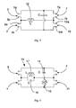
- FIG. 1 1 shows a schematic circuit diagram of the antenna architecture 1 with a 0 ° / 90 ° LC coupler, an antenna 3 formed from two identical individual antennas 3a, 3b and a terminating resistor 4.
- the input port 5 of the 0 ° / 90 ° LC coupler 2 is connected via the non-phase-shifting signal transmission path 6 with the first antenna port 7, to which the individual antenna 3a is connected.
- the input 5 is connected to the second Antennenausgangstor 9, to which the sub-antenna 3b is connected.
- the load gate 10 the terminating resistor 4 which is matched in its resistance value to the system impedance of the 0 ° / 90 ° coupler, is connected.
- each of the sub-antennas 3a, 3b must emit only half of the energy emitted by the power amplifier, so that thus the sub-antennas 3a, 3b must be designed for only half of the energy emitted by the power amplifier.
- the subantenna 3a, 3b must be designed compared to the classical solution with an antenna and insulators only for half the current carrying capacity, so that this antenna architecture can also be realized in media that was hardly possible for the classic design with an antenna.
- the arrangement is also much more robust against interference, since often only one of the two sub-antennas is detected by such a disorder.
- Another advantage is that the directional characteristic of the antenna 3 can be optimized, so that, for example, in a mobile phone, the electromagnetic load of a user can be reduced.
- the arrangement has the particular advantage that a wave reflected by an antenna or a wave traveling from the output into the circuit is absorbed in the terminating resistor 4 and thus is not reflected to the input port.
- LC coupler for example, a 0 ° / 90 ° hybrid coupler can be used, which is particularly suitable when the subantenna 3a, 3b and the input port 5 are constructed in unbalanced line technology. It is understood that other 0 ° / 90 ° couplers can be used.
- FIG. 2 shows a schematic circuit diagram of the antenna architecture 1 with a plurality of 0 ° / 90 ° -Koppplem connected in series.
- the power amplifier is connected to the input port 5 of the uppermost 0 ° / 90 ° coupler 2.
- the input port 5 of the second 0 ° / 90 ° coupler is connected.
- a plurality of 0 ° / 90 ° couplers 2 can thus be connected in series one behind the other, wherein an input port 5 of a 0 ° / 90 ° coupler is always connected to the load port 10 of the preceding 0 ° / 90 ° coupler and thus forms the terminating resistor , Only the last 0 ° / 90 ° coupler 2 in the row must then be completed with a matching terminating resistor 4.
- the 0 ° / 90 ° couplers in this series connection can then be advantageously designed to be dimensioned for different, mutually adjacent operating frequencies, thereby forming an ultra broad band (UWB) antenna and so that the antenna architecture over a wide frequency range can be used.
- UWB ultra broad band
- separate frequency bands can be controlled if the operating frequencies do not adjoin one another.
- FIG. 3 shows a 0 ° / 90 ° coupler 2, which can be realized in the manner described above only with a capacitance 11 and an inductance 12, and thus can be referred to as LC coupler.
- Each gate of the LC coupler 2 is formed from two gate clamps.
- Each gate terminal of a gate is connected to a gate terminal of the respective adjacent gate via an ideal line, so that in each case two to one Torklemme coincide.
- the gate terminal 5a of the entrance gate 5 is connected via an ideal line to the gate terminal 7a of the first further gate 7, so that these two coincide to form a common gate terminal.
- the Torklemmen 7b and 10, 10b and 9b and 9a and 5b fall together in each case to a common Torklemme, so that the LC coupler 2 actually has only four gate terminals.
- the capacitance 11 and the inductance 12 are connected between these four gate terminals so that the capacitance 11, the common gate terminal of the input gate 5 and the first further gate 7 with the common gate terminal of the load gate 10 and the second further gate 9, and the inductor 12th the common gate terminal of the input 5 and the antenna gate 9 connects to the common gate terminal of the first further gate 7 and the second further gate 10.
- the LC coupler is a mono-band 0 ° / 90 ° coupler for a working frequency of 2GHz.
- this 0 ° / 90 ° coupler is that one point of this circuit may be connected to ground, resulting in two unbalanced gates. If, for example, the common door terminal of the input door 5 and the antenna door 9 is connected to ground, unbalanced components can be connected to these two gates. Thus, it is a 0 ° / 90 ° coupler 2 with integrated balun functionality.
- the two individual antennas 3 a, 3 b and the input port 5 can be realized either in symmetrical ladder technology, or all three components must be realized in asymmetrical ladder technology.
- a balun must be connected between the gate and the component in a known manner in order to restore the symmetry.
- a so-called Balun balanced - unbalanced
- FIG. 4 shows a circuit diagram in which a mono-band coupler described above to a -90 ° / 90 ° dual-band coupler 13 is developed.
- the -90 ° / 90 ° coupler 13 has an input port 5 and an antenna port 9 and a first further port 7 and a second further port 10.
- the inductance and the capacitance used in the 0 ° / 90 ° coupler are here by a parallel resonant circuit, which is formed from the inductor 17 and the capacitor 16, and a series resonant circuit consisting of the capacitance 14 and the inductance 15 is formed replaced.
- the operation for the two operating frequencies of the dual-band coupler 13 is equal to that of the LC and the CL coupler.
- the dual-band coupler thus acts as a 90 ° coupler and for the higher operating frequency than -90 ° coupler. If one interchanges the parallel and the series resonant circuit in this variant of the coupler 13, then the dual-band coupler 13 behaves correspondingly at the lower operating frequency as a -90 ° coupler and at the higher operating frequency as a 90 ° coupler.
- the respective center frequencies of the two operating frequencies of the dual-band coupler must stand in no particular distance from each other.
Landscapes
- Transmitters (AREA)
- Radar Systems Or Details Thereof (AREA)
- Burglar Alarm Systems (AREA)
- Control Of Motors That Do Not Use Commutators (AREA)
Description
- Die Erfindung betrifft eine Antennenarchitektur gemäß dem Oberbegriff des Patentanspruchs 1.
- In einem modernen drahtlosen Kommunikationssystemen, wie zum Beispiel dem Mobilfimkstandard UMTS oder in einem drahtlos vernetzten Computernetzwerk, einem so genannten wireless local area network (WLAN), werden die zu übertragenden digitalen Daten über eine Funkverbindung im Gigahertzbereich übertragen. Beispielsweise werden im UMTS Standard Frequenzen zwischen 1,900 und 2,170 GHz und für ein WLAN Frequenzen um 2,4 GHz genutzt. Für Funksignale dieser Frequenzen liegen die Wellenlängen bei einigen Zentimetern und damit im Mikrowellenbereich. Funksignale dieser Wellenlänge sind damit durch vergleichsweise kleine Objekte zu stören, wobei die Störwirkung eines Objekts vom Abstand des Objekts zur Antenne und von der elektrischen Leitfähigkeit des Objekts abhängt. Je geringer der Abstand des Objekts zur Antenne und je größer dessen elektrische Leitfähigkeit ist, umso stärker wird das von der Antenne ausgesendete Funksignal gestört. Dabei kann die Störung einerseits bewirken, dass die Ausbreitung des Funksignals beeinträchtigt wird, andererseits kann das Funksignal in seiner Richtung umgelenkt, insbesondere reflektiert werden, so dass der reflektierte Anteil beispielsweise zur Antenne zurück gelenkt wird.
- Gegebenenfalls, und insbesondere in dem Fall, dass ein elektrisch gut leitendes Objekt sich in der Nähe der Antenne befindet, werden durch ein Objekt nicht nur die ausgestrahlten Signale in ihrer Ausbreitung gestört, sondern es kommt, beispielsweise durch den geringen Abstand, auch zu Veränderungen der Antennencharakteristik, insbesondere des Eingangswiderstands der Antenne.
- In der Praxis sind die Antennen eines solchen UMTS- oder WLAN-Gerätes nahezu direkt einem Leistungsverstärker verbunden, so dass für eine optimale Übertragung der Sendeleistung zwischen dem Leistungsverstärker und der Antenne eine Anpassung der Widerstände vorliegen muss. Im Idealzustand, wenn also kein störendes Objekt in der Nähe der Antenne die Antennencharakteristik verändert, liegt Anpassung vor. Ändert sich jedoch der Eingangswiderstand der Antenne, so führt dies zu einer Veränderung des Arbeitspunktes des Leistungsverstärkers und des Übertragungsverhaltens: In der Praxis steigt der Wert der Error Vector Magnitude (EVM-Wert), die als Maß für die Linearitätsabweichung von Hochfrequenz-Leistungsverstärkern herangezogen wird.
- Zur Erzielung einer hohen Datenübertragungsrate muss jedoch ein lineares Übertragungsverhalten des vorgeschalteten Leistungsverstärkers erreicht werden. Ein Verschiebung des Arbeitspunktes des Leistungsverstärkers, mit der ein steigender EVM-Wert einhergeht, ist damit nachteilig. Versuche, einen Leistungsverstärker in seinem Verhalten so robust auszulegen, dass ein elektrisch gut leitendes, nahes Objekt den Arbeitspunkt nicht beeinflusst, sind bis jetzt ohne Erfolg geblieben.
- Aus dem Stand der Technik ist bekannt, dass in solchen System so genannte "Isolatoren" eingesetzt werden, die zwischen die Antenne und den Leistungsverstärker geschaltet werden und den Leistungsverstärker von der Antenne "isolieren", um so Rückwirkungen auf den Leistungsverstärker zu verhindern. Diese Isolatoren bewirken damit, dass der Arbeitspunkt des Leistungsverstärkers nicht aus dem Idealpunkt verschoben wird. Weiterhin wird neben diesen aus passiven Bauelementen bestehenden Isolatoren an elektronischen Regellösungen gearbeitet, bei denen elektronische Regler eingesetzt werden. Solche Isolatoren sowie elektronische Regellösungen werden beispielsweise beschrieben in Bezooijen A., Chanlo Ch., Roermund, A.H.M., Adaptively Preserving Power Amplifier Linearity under Antenna Mismatch, IMS2004, Fort Worth.
- Der Einsatz solcher aus dem Stand der Technik bekannten Isolatoren bringt mehrere Nachteile mit sich. Isolatoren sind teuer, sie benötigen viel Raum und weisen im Vergleich zu anderen Bauteilen ein hohes Gewicht auf. Weiterhin weisen sie eine hohe Dämpfung auf, so dass die von dem Leistungsverstärker abgegebene Ausgangsleistung nicht optimal an die Antenne übertragen und damit abgestrahlt wird. Dies führt zu einer erhöhten Leistungsaufnahme durch den Verstärker und damit insbesondere in batteriebetriebenen Mobilfunkgeräten, wie beispielsweise UMTS-Mobiltelefonen, so genannten Handsets, dazu, dass die Batterien bzw. Akkus schnell leer sind. Weiterhin können die auf elektronischer Regelung basierenden Isolatoren auf Grund des zurück geführten Regelkreises zur Instabilität neigen, was gegebenenfalls weitere unerwünschte Störungen verursacht. Der Einsatz derartiger Isolatoren zur Entkopplung der Antenne von dem Leistungsverstärker ist somit zwar möglich, jedoch mit großen Nachteilen und Schwierigkeiten verbunden.
Eine gattungsgemäße Antennenarchitektur ist aus derWO 2004/051878 A1 und derUS 3,375,524 bekannt. - Aufgabe der Erfindung ist es somit, eine rückwirkungsfreie und angepasste Antennenarchitektur vorzuschlagen. Um dies zu erreichen soll eine Schaltung vorgeschlagen werden, die mit möglichst wenigen und einfachen Bauelementen realisiert werden kann.
- Zur Lösung dieser Aufgabe wird eine Antennenarchitektur mit den Merkmalen.
- In vorliegendem Zusammenhang umfasst der Begriff "LC-Koppler" sämtlicher Kopplerarchitekturen, die auf "lumped elements", also auf konzentrierte Bauteile, wie SMD-Bauelemente, Dünnschicht oder Dickschichtelemente, Halbleiterelemente, Kondensatoren oder Spulen und ähnliche Baugruppen, zurückgreifen.
- Der LC-Koppler weist ein Lasttor auf, an welchem ein von einer Antenne nicht abgestrahltes und reflektiertes Signal ausgekoppelt werden kann, so dass auf einfache und betriebssichere Weise sichergestellt wird, dass dieses reflektierte Signal einen Leistungsverstärker nicht mehr erreicht.
- Die vorgeschlagene Antennenarchitektur besteht damit vorzugsweise aus einem viertorigen 0°/90°-LC-Koppler und einer Antenne, die aus zwei baugleichen Einzelantennen gebildet ist sowie einem Abschluss- oder Lastwiderstand, der in seinem Widerstandswert der Systemimpedanz angepasst ist. Das Eingangstor des LC-Kopplers wird mit dem Leistungsverstärker verbunden und das Lasttor wird mit dem Abschlusswiderstand abgeschlossen. Jede der beiden baugleichen Einzelantennen wird an jeweils ein Antennentor angeschlossen.
- Der LC-Koppler bewirkt, dass eine vom Ausgang in den LC-Koppler hineinlaufende Welle letztlich in dem angepassten Abschlusswiderstand absorbiert wird. Somit werden Wellenanteile, die an einem nahe an der Antenne befindlichen Objekt reflektiert und von einer der Einzelantennen empfangen werden, in dem Abschlusswiderstand des LC-Kopplers absorbiert und wirken damit nicht auf den Leistungsverstärker zurück. Insofern wirkt der LC-Koppler für diese vom Ausgang her in die Schaltung einlaufenden Wellen wie ein Isolator gegenüber dem Leistungsverstärker, so dass der 0°/90°-Koppler in Verbindung mit den beiden Einzelantennen eine Isolatorantenne bildet.
- Zur möglichst einfachen Realisierung einer solchen Antennenarchitektur wird alternativ bzw. kumulativ ein 0°/90°-Koppler vorgeschlagen, der ein Eingangstor, ein Lasttor sowie ein weiteres erstes und ein weiteres zweites Tor aufweist, wobei jedes Tor jeweils aus einer ersten und einer zweiten Torklemme gebildet ist. Zwischen den Torklemmen benachbarter Tore befinden sich keine in dem Arbeitsfrequenzbereich wesentlich wirksame, also ohmsche oder sonst wie Signale beeinflussende Bauelemente, so dass zwei Torklemmen benachbarter Tore jeweils zu einer Torklemme zusammenfallen und eine gemeinsame Torklemme bilden können, wobei selbstverständlich vernachlässigbare und nie ganz vermeidbare Restwiderstände, - induktivitäten und -kapazitäten vorliegen bzw. vorliegen können. Eine derartige Anordnung wird vorliegend als kurzgeschlossen bezeichnet, so dass die erste Torklemme des Eingangstores und die erste Torklemme des ersten weiteren Tores kurzgeschlossen sind, die zweite Torklemme des Eingangstores und die erste Torklemme des Lasttores kurzgeschlossen sind, die zweite Torklemme des ersten weiteren Tores und die erste Torklemme des zweiten weiteren Tores kurzgeschlossen sind sowie die zweite Torklemme des zweiten weiteren Tores und die zweite Torklemme des Lasttores kurzgeschlossen sind.
- Damit ist vorzugsweise die erste Torklemme des Eingangstores die erste Torklemme des ersten weiteren Tores und die zweite Torklemme des Eingangstores die erste Torklemme des Lasttores. Die zweite Torklemme des ersten weiteren Tores ist die erste Torklemme des zweiten weiteren Tores und dessen zweite Torklemme ist vorzugsweise die zweite Torklemme des Lasttores. Der 0°/90°-Koppler weist somit dann nur vier Torklemmen auf.
- Der LC-Koppler ist nun dadurch gekennzeichnet, dass die erste Torklemme des Eingangstores über ein erstes LC-Glied mit der zweiten Klemme des zweiten weiteren Tores und die zweite Torklemme des Eingangstores über ein zweites LC-Glied mit der zweiten Torklemme des ersten weiteren Tores verbunden ist, und dass die Dimensionierung der beiden LC-Glieder im vorgesehenen Arbeitsfrequenzbereich zwischen den beiden Signalübertragungspfaden eine Phasenverschiebung von 90° bewirkt.
- Damit lässt sich der 0°/90°-Koppler insbesondere mit nur zwei passiven Bauelementen realisieren, die im Bereich der Arbeitsfrequenz des 0°/90°-Kopplers die gewünschte Phasenverschiebung in den Signalübertragungspfaden bewirken.
- Aus dem Stand der Technik sind andererseits Koppler als Möglichkeit bekannt, zwei signalführende Kreise so miteinander zu verbinden, dass ein Austausch der Signale stattfinden kann. So ist in der Fachliteratur, "Messsysteme der Hochfrequenztechnik", Burkhard Schiek, Hütbig Verlag 1984, ein Leitungskoppler als Möglichkeit zur definierten Signalabschwächung oder Signaldämpfung erwähnt, und es ist angegeben, dass Koppler dazu eingesetzt werden können, Signale auf mehrere Tore aufzuteilen. Schließlich ist angegeben, dass Leitungskoppler dafür eingesetzt werden können, zwei Signale mit breitbandig 90°-Phasenverschiebung zu erzeugen. Als Beispiel ist zum einen ein abstrakt skizzierter Ringkoppler angegeben. Weiterhin ist ein resistiver Koppler erwähnt, der ausschließlich Wirkwiderstände, also rein ohmsche Widerstände als Kopplerwiderstände aufweist und für den eine Beispielrechnung zur Bestimmung der Dämpfung angegeben ist. Eine Phasenverschiebung zwischen den Toren ist bei diesem resistiven Koppler auf Grund der Verwendung der reinen Wirkwiderstände nicht möglich. Zu diesem resistiven Koppler ist schließlich angegeben, dass die Kopplerwiderstände auch komplex sein können. So könne beispielsweise der eine Wirkwiderstand durch eine Induktivität und der andere Wirkwiderstand durch eine Kapazität ersetzt sein. Damit sei der Koppler dann zwar verlustlos und zu einem Tor breitbandig entkoppelt, jedoch werde die Kopplung selbst frequenzabhängig.
- Die Verwendung von "lumped elements" ermöglicht es bei den erfindungsgemäßen LC-Kopplern die elektrische Länge auf 20° zu begrenzen. Hierdurch können die entsprechenden Koppler sehr klein gebaut werden und insbesondere auch in mobilen Geräten ohne weiteres zur Anwendung kommen. Andererseits versteht es sich, dass die Begrenzung der elektrischen Länge der Koppler auf 20° bzw. 18° oder insbesondere 15° auch unabhängig von der Verwendung von "lumped elements" vorteilhaft ist, um baulich kleine und robuste Antennenarchitekturen zur rückwirkungsfreien Verbindung einer Antenne mit einem Leistungsverstärker bereitzustellen, bei welchen die Antenne über einen Koppler an den Leistungsverstärker angeschlossen ist, wobei der Koppler zur Einspeisung des an die Antenne zu übertragenden Signals ein Eingangstor sowie zur Übertragung des Signals an die Antenne ein erstes und ein zweites Antennentor aufweist, wobei die Antenne eine erste und eine zweite, baugleiche Einzelantenne aufweist, wobei die erste Einzelantenne an das erste Antennentor und die zweite Einzelantenne an das zweite Antennentor angeschlossen ist, wobei das Lasttor abgeschlossen ist, und wobei der Koppler das Signal auf das erste Antennentor mit einer ersten Phase und auf das zweite Antennentor mit einer zweiten, um 90° gegenüber der ersten Phase verschobenen Phase überträgt.
- Es gibt nun mehrere Möglichkeiten, die erfindungsgemäße Antennenarchitektur und den 0°/90°-LC-Koppler in vorteilhafter Art und Weise auszugestalten. Im Folgenden werden nun mehrere bevorzugte Ausführungsbeispiele der Antennearchitektur und des 0°/90°-LC-Kopplers anhand von Zeichnungen beschrieben. Dabei zeigt
- Figur 1:
- eine schematische Schaltskizze der Antennenarchitektur;
- Figur 2:
- eine schematische Schaltskizze der Antennenarchitektur mit mehreren, in Reihe geschalteten 0°/90°-Kopplern;
- Figur 3:
- eine Schaltskizze eines 0°/90°-Kopplers; und
- Figur 4
- eine Schaltskizze eines -90°/90°-Dual-Band-Kopplers.
-
Figur 1 zeigt eine schematische Schaltskizze der Antennenarchitektur 1 mit einem 0°/90°-LC-Koppler, einer aus zwei baugleichen Einzelantennen 3a, 3b gebildeten Antenne 3 und einem Abschlusswiderstand 4. Das Eingangstor 5 des 0°/90°-LC-Kopplers 2 ist über den nicht phasenverschiebenden Signalübertragungspfad 6 mit dem ersten Antennentor 7 verbunden, an das die Einzelantenne 3a angeschlossen ist. Über den um 90°-phasenverschiebenden Signalübertragungspfad 8 ist der Eingang 5 mit dem zweiten Antennenausgangstor 9 verbunden, an dem die Teilantenne 3b angeschlossen ist. An dem vierten Tor des LC-Kopplers, dem Lasttor 10, ist der in seinem Widerstandswert an die Systemimpedanz des 0°/90°-Kopplers angepasste Abschlusswiderstand 4 angeschlossen. - Läuft nun eine Welle von einem hier nicht dargestellten Leistungsverstärker über das Eingangstor 5 in den 0°/90°-Koppler 2, so wird diese zum Einen über den nicht phasenverschiebenden Signalübertragungspfad 6 zu dem ersten Antennentor 7 und damit auf die Teilantenne 3a übertragen. Zum anderen wird die Welle über den 90° phasenverschiebenden Signalübertragungspfad 8 zu dem zweiten Antennentor 9 und damit auf die zweite Teilantenne 3b übertragen. Das in den 0°/90°-Koppler eingespeiste Wellensignal wird so auf die beiden Signalübertragungspfade 6, 8 aufgeteilt und von der ersten Teilantenne 3a ohne Phasenverschiebung und von der zweiten Teilantenne 3b mit einer Phasenverschiebung von 90° abgestrahlt.
- Damit muss jede der Teilantennen 3a, 3b nur die Hälfte der vom Leistungsverstärker abgegebenen Energie abstrahlen, so dass damit die Teilantennen 3a, 3b nur für die Hälfte der vom Leistungsverstärker abgegebenen Energie ausgelegt sein müssen. Damit müssen die Teilantennen 3a, 3b gegenüber der klassischen Lösung mit einer Antenne und Isolatoren nur noch für die halbe Stromtragfähigkeit ausgelegt sein, so dass diese Antennenarchitektur auch in Medien realisiert werden kann, die für den klassischen Aufbau mit einer Antenne kaum möglich war. Die Anordnung wird darüber hinaus auch gegenüber Störeinflüssen wesentlich robuster, da häufig lediglich eine der beiden Teilantennen von einer derartigen Störung erfasst wird.
- Ein weiterer Vorteil liegt darin, dass die Richtcharakteristik der Antenne 3 optimiert werden kann, so dass beispielsweise bei einem Mobilfunktelefon die elektromagnetische Belastung eines Benutzers gesenkt werden kann.
- Die Anordnung hat insbesondere den Vorteil, dass eine von einer Antenne reflektierte Welle bzw. eine vom Ausgang in die Schaltung laufende Welle in dem Abschlusswiderstand 4 absorbiert und somit nicht zu dem Eingangstor reflektiert wird.
- Als LC-Koppler kann beispielsweise ein 0°/90° Hybrid-Koppler eingesetzt werden, der besonders geeignet ist, wenn die Teilantennen 3a, 3b und das Eingangstor 5 in unsymmetrischer Leitungstechnik aufgebaut werden. Es versteht sich, dass auch andere 0°/90°-Koppler zur Anwendung kommen können.
-
Figur 2 zeigt eine schematische Schaltskizze der Antennenarchitektur 1 mit mehreren, in Reihe geschalteten 0°/90°-Kopplem. Dabei ist der Leistungsverstärker an das Eingangstor 5 des obersten 0°/90°-Kopplers 2 angeschlossen. An das Lasttor 10 des ersten 0°/90°-Kopplers 2 ist das Eingangstor 5 des zweiten 0°/90°-Kopplers angeschlossen. Mehrere 0°/90°-Koppler 2 können so in Reihe hintereinander geschaltet sein, wobei ein Eingangstor 5 eines 0°/90°-Kopplers immer an das Lasttor 10 des vorhergehenden 0°/90°-Kopplers angeschlossen ist und damit dessen Abschlusswiderstand bildet. Nur der letzte 0°/90°-Koppler 2 in der Reihe muss dann mit einem angepassten Abschlusswiderstand 4 abgeschlossen sein. Die 0°/90°-Koppler in dieser Reihenschaltung können dann vorteilhaft so ausgelegt sein, dass sie für verschiedene, aneinander angrenzende Arbeitsfrequenzen dimensioniert sind, so dass dadurch eine Ultra-Breitband Antenne bzw. UWB-Antenne (ultra wide band) gebildet ist und damit die Antennenarchitektur über eine breiten Frequenzbereich eingesetzt werden kann. Andererseits können getrennt Frequenzbänder angesteuert werden, wenn die Arbeitsfrequenzen nicht aneinander grenzen. -
Figur 3 zeigt einen 0°/90°-Koppler 2, der in der oben beschriebenen Weise nur mit einer Kapazität 11 und einer Induktivität 12 realisiert und damit als LC-Koppler bezeichnet werden kann. Jedes Tor des LC-Kopplers 2 ist aus jeweils zwei Torklemmen gebildet. Jede Torklemme eines Tores ist dabei mit einer Torklemme des jeweils benachbarten Tores über eine ideale Leitung verbunden, so dass jeweils zwei zu einer Torklemme zusammenfallen. So ist beispielsweise die Torklemme 5a des Eingangstores 5 über eine ideale Leitung mit der Torklemme 7a des ersten weiteren Tores 7 verbunden, so dass diese beiden zu einer gemeinsamen Torklemme zusammenfallen. Ebenso fallen die Torklemmen 7b und 10, 10b und 9b sowie 9a und 5b zu jeweils einer gemeinsamen Torklemme zusammen, so dass der LC-Koppler 2 tatsächlich nur vier Torklemmen aufweist. Die Kapazität 11 und die Induktivität 12 sind dabei zwischen diesen vier Torklemmen so geschaltet, dass die Kapazität 11 die gemeinsame Torklemme des Eingangstores 5 und des ersten weiteren Tores 7 mit der gemeinsamen Torklemme des Lasttores 10 und des zweiten weiteren Tores 9, und die Induktivität 12 die gemeinsame Torklemme des Eingangs- 5 und des Antennentores 9 mit der gemeinsamen Torklemme des ersten weiteren Tores 7 und des zweiten weiteren Tores 10 verbindet. - Die für die Funktion des 0°/90°-Kopplers 2 notwendige Phasenverschiebung erhält man für die vorgesehene Arbeitsfrequenz des LC-Kopplers über eine geeignete Dimensionierung der Kapazität 11 und der Induktivität 12, für die im Folgenden nach den bekannten Rechenregeln ein kurzes Beispiel ausgeführt ist.
- In diesem Beispiel sei die Systemimpedanz des LC-Kopplers Z0=50 Ohm und die Arbeitsfrequenz sei f0=2 GHz. Der Widerstand Z1 einer Kapazität C und der Widerstand Z2 einer Induktivität L lassen sich dann bestimmen zu


Mit den für einen Resonanzkreis bekannten Bedingungen - 1. Z1 + Z2 = 0 und
- 2. Z1 * Z2 = Z0 2 lassen sich die Werte für die Induktivität L und der Kapazität C bestimmen zu


- Mit dieser Dimensionierung der Kapazität und der Induktivität wird für die gewählte Arbeitsfrequenz von 2 GHz eine Phasenverschiebung von 0° bzw. 90° erreicht. Damit ist der LC-Koppler ein Mono-Band 0°/90°-Koppler für eine Arbeitsfrequenz von 2GHz.
- Eine Besonderheit dieses 0°/90°-Kopplers ist, dass ein Punkt dieser Schaltung mit Masse verbunden werden darf, so dass zwei unsymmetrische Tore entstehen. Wird beispielsweise die gemeinsame Torklemme des Eingangstores 5 und des Antennentores 9 mit Masse verbunden, so können an diese beiden Tore unsymmetrische Komponenten angeschlossen werden. Somit handelt es sich um einen 0°/90°-Koppler 2 mit integrierter Balunfunktionalität.
- Vertauscht man die Platzierung von Kapazität 11 und Induktivität 12, so ergibt sich ein 0°/-90°-Koppler, der alternativ genutzt werden kann.
- Weiterhin können bei diesem 0°/90°-Koppler die beiden Einzelantennen 3a, 3b und das Eingangstor 5 entweder in symmetrischer Leitertechnik realisiert sein, oder es müssen alle drei Komponenten in unsymmetrischer Leitertechnik realisiert sein. Soll dagegen eine anzuschließende Komponente unsymmetrisch zu den anderen ausgelegt sein, so ist in bekannter Weise zur Wiederherstellung der Symmetrie ein Symmetrierglied zwischen das Tor und die Komponente zu schalten. Hier kann beispielsweise ein so genannter Balun (balanced - unbalanced) eingesetzt werden, der beispielsweise als Transformator realisiert sein kann.
-
Figur 4 zeigt eine Schaltskizze, in der ein oben beschriebener Mono-Band-Koppler zu einem -90°/90°-Dual-Band-Koppler 13 weitergebildet ist. Ebenso wie der zuvor beschriebene Mono-Band-0°/90°-Koppler 2 weist der -90°/90°-Koppler 13 ein Eingangstor 5 und ein Antennentor 9 sowie ein erstes weiteres Tor 7 und ein zweites weiteres Tor 10 auf. Die in dem 0°/90°-Koppler eingesetzte Induktivität und die Kapazität sind hier durch einen Parallelschwingkreis, der aus der Induktivität 17 und der Kapazität 16 gebildet ist, bzw. einen Serienschwingkreis, der aus der Kapazität 14 und der Induktivität 15 gebildet ist, ersetzt. Die Funktionsweise für die beiden Arbeitsfrequenzen des Dual-Band-Kopplers 13 ist gleich der des LC- und des CL-Kopplers. Für die tiefere der beiden Arbeitsfrequenzen des Dual-Band-Kopplers 13 wirkt der Dual-Band-Koppler damit als 90°-Koppler und für die höhere Arbeitsfrequenz als -90°-Koppler. Vertauscht man in dieser Variante des Kopplers 13 den Parallel- mit dem Serienschwingkreis, so verhält sich der Dual-Band-Koppler 13 bei der tieferen Arbeitsfrequenz entsprechend als -90°-Koppler und bei der höheren Arbeitsfrequenz als 90°-Koppler. Die jeweiligen Mittenfrequenzen der beiden Arbeitsfrequenzen des Dual-Band-Kopplers müssen dabei in keinem besonderen Abstand zueinander stehen.
Claims (2)
- Antennenarchitektur (1) zur rückwirkungsfreien Verbindung einer Antenne (3) mit einem Leistungsverstärker, wobei die Antenne (3) über einen Koppler (2) an den Leistungsverstärker angeschlossen ist, wobei der Koppler (2) zur Einspeisung des an die Antenne (3) zu übertragenden Signals ein Eingangstor (5) sowie zur Übertragung des Signals an die Antenne (3) ein erstes und ein zweites Antennentor (7, 9) aufweist, wobei die Antenne (3) eine erste und eine zweite Einzelantenne (3a, 3b) aufweist, wobei die erste Einzelantenne (3a) an das erste Antennentor (7) und die zweite Einzelantenne (3b) an das zweite Antennentor (9) angeschlossen ist und wobei der Koppler (2) das Signal auf das erste Antennentor (7) mit einer ersten Phase und auf das zweite Antennentor (9) mit einer zweiten, um 90° gegenüber der ersten Phase verschobenen Phase überträgt, dadurch gekennzeichnet, dass der Koppler (2) ein LC-Koppler ist dessen Tore aus jeweils zwei Torklemmen (5a, 5b, 7a, 7b, 9a, 9b, 10a, 10b) gebildet sind,, die erste und die zweite Einzelantenne baugleich und die Einzelantennen (3a, 3b) jeweils in symmetrischer Leitertechnik ausgeführt sind, das Lasttor (10) mit einem angepassten Abschlusswiderstand abgeschlossen ist und das Eingangstor (5) in unsymmetrischer Leitungstechnik aufgebant ist indem die Torklemmen des Eingangstores (5) und des Antennentores (9) mit einander verbander und an Masse gelegt sind, damit der Koppler (2) eine integrierte Balunfunktionalität aufweist.
- Antennenarchitektur (1) nach Anspruch 1, dadurch gekennzeichnet, dass der Abschlusswiderstand (4) mindestens einen weiteren Koppler, vorzugsweise einen weiteren LC-Koppler, mit einer Antenne aufweist und der weitere Koppler zur Einspeisung des an seine Antenne zu übertragenden Signals ein Eingangstor und zur Übertragung des Signals an seine Antenne ein erstes und ein zweites Antennentor und weiterhin ein Lasttor aufweist, dass seine Antenne eine erste und eine zweite, baugleiche Einzelantenne aufweist, wobei seine erste Einzelantenne an sein erste Antennentor und seine zweite Einzelantenne an sein zweite Antennentor angeschlossen ist, dass sein Lasttor abgeschlossen ist, und dass der Koppler das Signal auf sein erstes Antennentor mit einer ersten Phase und auf sein zweites Antennentor mit einer zweiten, um 90° gegenüber der ersten Phase verschobenen Phase überträgt.
Applications Claiming Priority (2)
| Application Number | Priority Date | Filing Date | Title |
|---|---|---|---|
| DE102004054442A DE102004054442A1 (de) | 2004-11-10 | 2004-11-10 | Antennenarchitektur und Koppler |
| PCT/DE2005/002002 WO2006050701A2 (de) | 2004-11-10 | 2005-11-08 | Antennenarchitektur und lc-koppler |
Publications (2)
| Publication Number | Publication Date |
|---|---|
| EP1813032A2 EP1813032A2 (de) | 2007-08-01 |
| EP1813032B1 true EP1813032B1 (de) | 2009-02-25 |
Family
ID=35695714
Family Applications (1)
| Application Number | Title | Priority Date | Filing Date |
|---|---|---|---|
| EP05807888A Expired - Lifetime EP1813032B1 (de) | 2004-11-10 | 2005-11-08 | Antennenarchitektur und lc-koppler |
Country Status (5)
| Country | Link |
|---|---|
| US (1) | US7812780B2 (de) |
| EP (1) | EP1813032B1 (de) |
| AT (1) | ATE424062T1 (de) |
| DE (3) | DE102004054442A1 (de) |
| WO (1) | WO2006050701A2 (de) |
Families Citing this family (1)
| Publication number | Priority date | Publication date | Assignee | Title |
|---|---|---|---|---|
| DE102005058875B4 (de) | 2005-12-09 | 2016-02-25 | Infineon Technologies Ag | Anpassnetzwerk |
Citations (1)
| Publication number | Priority date | Publication date | Assignee | Title |
|---|---|---|---|---|
| US3375524A (en) * | 1963-10-10 | 1968-03-26 | Siemens Ag | Antenna distributor circuit for four dipoles with adjacent dipoles in phase quadrature |
Family Cites Families (9)
| Publication number | Priority date | Publication date | Assignee | Title |
|---|---|---|---|---|
| GB1207511A (en) | 1967-01-04 | 1970-10-07 | Ass Elect Ind | Improvements in dielectric heating apparatus |
| US4101901A (en) * | 1975-12-22 | 1978-07-18 | Motorola, Inc. | Interleaved antenna array for use in a multiple input antenna system |
| US4218685A (en) * | 1978-10-17 | 1980-08-19 | Nasa | Coaxial phased array antenna |
| CA1208714A (en) * | 1983-09-22 | 1986-07-29 | Igor Miletic | Rf hybrid |
| DE3523876C1 (de) * | 1985-07-04 | 1986-09-25 | Rohde & Schwarz GmbH & Co KG, 8000 München | Antennenumschalteinrichtung |
| FR2741221B1 (fr) * | 1995-11-13 | 1997-12-05 | Alcatel Telspace | Etage de demodulation directe d'un signal module en quadrature de phase et recepteur comprenant un tel etage de demodulation |
| EP1341258A1 (de) * | 1998-06-26 | 2003-09-03 | Thales Antennas Limited | Verfahren und Anordnung für Signalkopplung |
| GB2395843B (en) | 2002-11-29 | 2006-04-26 | Motorola Inc | Wireless subscriber communication unit and antenna arrangement therefor |
| US7206566B1 (en) * | 2004-07-21 | 2007-04-17 | Hrl Laboratories, Llc | Apparatus and method for frequency conversion |
-
2004
- 2004-11-10 DE DE102004054442A patent/DE102004054442A1/de not_active Withdrawn
-
2005
- 2005-11-08 US US11/667,508 patent/US7812780B2/en not_active Expired - Fee Related
- 2005-11-08 EP EP05807888A patent/EP1813032B1/de not_active Expired - Lifetime
- 2005-11-08 AT AT05807888T patent/ATE424062T1/de active
- 2005-11-08 WO PCT/DE2005/002002 patent/WO2006050701A2/de not_active Ceased
- 2005-11-08 DE DE112005003391T patent/DE112005003391A5/de not_active Withdrawn
- 2005-11-08 DE DE502005006715T patent/DE502005006715D1/de not_active Expired - Lifetime
Patent Citations (1)
| Publication number | Priority date | Publication date | Assignee | Title |
|---|---|---|---|---|
| US3375524A (en) * | 1963-10-10 | 1968-03-26 | Siemens Ag | Antenna distributor circuit for four dipoles with adjacent dipoles in phase quadrature |
Also Published As
| Publication number | Publication date |
|---|---|
| ATE424062T1 (de) | 2009-03-15 |
| US20080030421A1 (en) | 2008-02-07 |
| DE102004054442A1 (de) | 2006-05-24 |
| EP1813032A2 (de) | 2007-08-01 |
| DE502005006715D1 (de) | 2009-04-09 |
| DE112005003391A5 (de) | 2007-10-18 |
| US7812780B2 (en) | 2010-10-12 |
| WO2006050701A2 (de) | 2006-05-18 |
| WO2006050701A3 (de) | 2006-07-20 |
Similar Documents
| Publication | Publication Date | Title |
|---|---|---|
| EP1012899B1 (de) | Vorrichtung zur kontaktlosen übertragung elektrischer signale und/oder energie | |
| DE102010040290B4 (de) | Richtkoppler | |
| DE102010046677B4 (de) | Schaltungsanordnung | |
| DE102011012927B4 (de) | Verstärkermodul | |
| DE69730389T2 (de) | Tiefpassfilter mit richtkoppler und tragbares telefon damit | |
| DE60306513T2 (de) | Antennenanordnung | |
| DE69835937T2 (de) | Zweifrequenzschalter, anordnung mit gemeinsamer zweifrequenzantenne und mobile zweifrequenz-funkübertragungsausrüstung damit | |
| DE69929968T2 (de) | Antennenschalter | |
| DE10114769B4 (de) | Aktive Breitbandempfangsantenne | |
| EP1406349B1 (de) | Aktive Breitband-Empfangsantenne mit Empfangspegel-Regelung | |
| EP1114523A1 (de) | Mehrband-antennenschalter | |
| DE60128700T2 (de) | Drahtloses funkgerät | |
| DE10158791A1 (de) | Hochfrequenzverstärker und Funkübertragungsvorrichtung | |
| DE10247025A1 (de) | Differenzfunkvorrichtung | |
| DE112013006963T5 (de) | Schaltungsanorderung | |
| DE102022201807A1 (de) | Intelligenter bidirektionaler koppler mit schaltbaren induktoren | |
| DE69624377T2 (de) | Antennenverstärker | |
| DE102013013579A1 (de) | Kombinierer/Teiler mit Verbindungsstruktur | |
| DE10102891A1 (de) | Hochleistungsverstärker mit Verstärkerelement, dazugehörige Funkübertragungseinrichtung und Meßeinrichtung dafür | |
| EP1388206B1 (de) | Filteranordnung fuer symmetrische und unsymmetrische leitungssysteme | |
| DE102012018651A1 (de) | Leistungsweiche/-kombinator/-teiler | |
| DE102014102704A1 (de) | Kombinierte Impedanzanpass- und HF-Filterschaltung | |
| DE102006046190B4 (de) | Schaltungsanordnung, Verfahren zum Betreiben einer Schaltungsanordnung und Verfahren zum Betreiben eines Dual-Mode-UMTS/GSM-Mobiltelefons | |
| CN109193163A (zh) | 基于枝节加载谐振器的三频滤波天线、无线电系统射频前端 | |
| EP1813032A2 (de) | Antennenarchitektur und lc-koppler |
Legal Events
| Date | Code | Title | Description |
|---|---|---|---|
| PUAI | Public reference made under article 153(3) epc to a published international application that has entered the european phase |
Free format text: ORIGINAL CODE: 0009012 |
|
| 17P | Request for examination filed |
Effective date: 20070606 |
|
| AK | Designated contracting states |
Kind code of ref document: A2 Designated state(s): AT BE BG CH CY CZ DE DK EE ES FI FR GB GR HU IE IS IT LI LT LU LV MC NL PL PT RO SE SI SK TR |
|
| RIN1 | Information on inventor provided before grant (corrected) |
Inventor name: HEUERMANN, HOLGER |
|
| 17Q | First examination report despatched |
Effective date: 20071127 |
|
| DAX | Request for extension of the european patent (deleted) | ||
| GRAP | Despatch of communication of intention to grant a patent |
Free format text: ORIGINAL CODE: EPIDOSNIGR1 |
|
| GRAS | Grant fee paid |
Free format text: ORIGINAL CODE: EPIDOSNIGR3 |
|
| GRAA | (expected) grant |
Free format text: ORIGINAL CODE: 0009210 |
|
| AK | Designated contracting states |
Kind code of ref document: B1 Designated state(s): AT BE BG CH CY CZ DE DK EE ES FI FR GB GR HU IE IS IT LI LT LU LV MC NL PL PT RO SE SI SK TR |
|
| REG | Reference to a national code |
Ref country code: GB Ref legal event code: FG4D Free format text: NOT ENGLISH |
|
| REG | Reference to a national code |
Ref country code: CH Ref legal event code: EP |
|
| REG | Reference to a national code |
Ref country code: IE Ref legal event code: FG4D Free format text: LANGUAGE OF EP DOCUMENT: GERMAN |
|
| REF | Corresponds to: |
Ref document number: 502005006715 Country of ref document: DE Date of ref document: 20090409 Kind code of ref document: P |
|
| REG | Reference to a national code |
Ref country code: CH Ref legal event code: NV Representative=s name: E. BLUM & CO. AG PATENT- UND MARKENANWAELTE VSP |
|
| PG25 | Lapsed in a contracting state [announced via postgrant information from national office to epo] |
Ref country code: LT Free format text: LAPSE BECAUSE OF FAILURE TO SUBMIT A TRANSLATION OF THE DESCRIPTION OR TO PAY THE FEE WITHIN THE PRESCRIBED TIME-LIMIT Effective date: 20090225 Ref country code: SI Free format text: LAPSE BECAUSE OF FAILURE TO SUBMIT A TRANSLATION OF THE DESCRIPTION OR TO PAY THE FEE WITHIN THE PRESCRIBED TIME-LIMIT Effective date: 20090225 Ref country code: FI Free format text: LAPSE BECAUSE OF FAILURE TO SUBMIT A TRANSLATION OF THE DESCRIPTION OR TO PAY THE FEE WITHIN THE PRESCRIBED TIME-LIMIT Effective date: 20090225 |
|
| PG25 | Lapsed in a contracting state [announced via postgrant information from national office to epo] |
Ref country code: PL Free format text: LAPSE BECAUSE OF FAILURE TO SUBMIT A TRANSLATION OF THE DESCRIPTION OR TO PAY THE FEE WITHIN THE PRESCRIBED TIME-LIMIT Effective date: 20090225 Ref country code: IS Free format text: LAPSE BECAUSE OF FAILURE TO SUBMIT A TRANSLATION OF THE DESCRIPTION OR TO PAY THE FEE WITHIN THE PRESCRIBED TIME-LIMIT Effective date: 20090625 Ref country code: SE Free format text: LAPSE BECAUSE OF FAILURE TO SUBMIT A TRANSLATION OF THE DESCRIPTION OR TO PAY THE FEE WITHIN THE PRESCRIBED TIME-LIMIT Effective date: 20090525 Ref country code: LV Free format text: LAPSE BECAUSE OF FAILURE TO SUBMIT A TRANSLATION OF THE DESCRIPTION OR TO PAY THE FEE WITHIN THE PRESCRIBED TIME-LIMIT Effective date: 20090225 |
|
| REG | Reference to a national code |
Ref country code: IE Ref legal event code: FD4D |
|
| PG25 | Lapsed in a contracting state [announced via postgrant information from national office to epo] |
Ref country code: DK Free format text: LAPSE BECAUSE OF FAILURE TO SUBMIT A TRANSLATION OF THE DESCRIPTION OR TO PAY THE FEE WITHIN THE PRESCRIBED TIME-LIMIT Effective date: 20090225 Ref country code: CZ Free format text: LAPSE BECAUSE OF FAILURE TO SUBMIT A TRANSLATION OF THE DESCRIPTION OR TO PAY THE FEE WITHIN THE PRESCRIBED TIME-LIMIT Effective date: 20090225 Ref country code: PT Free format text: LAPSE BECAUSE OF FAILURE TO SUBMIT A TRANSLATION OF THE DESCRIPTION OR TO PAY THE FEE WITHIN THE PRESCRIBED TIME-LIMIT Effective date: 20090812 Ref country code: EE Free format text: LAPSE BECAUSE OF FAILURE TO SUBMIT A TRANSLATION OF THE DESCRIPTION OR TO PAY THE FEE WITHIN THE PRESCRIBED TIME-LIMIT Effective date: 20090225 Ref country code: ES Free format text: LAPSE BECAUSE OF FAILURE TO SUBMIT A TRANSLATION OF THE DESCRIPTION OR TO PAY THE FEE WITHIN THE PRESCRIBED TIME-LIMIT Effective date: 20090605 Ref country code: IE Free format text: LAPSE BECAUSE OF FAILURE TO SUBMIT A TRANSLATION OF THE DESCRIPTION OR TO PAY THE FEE WITHIN THE PRESCRIBED TIME-LIMIT Effective date: 20090225 |
|
| PG25 | Lapsed in a contracting state [announced via postgrant information from national office to epo] |
Ref country code: SK Free format text: LAPSE BECAUSE OF FAILURE TO SUBMIT A TRANSLATION OF THE DESCRIPTION OR TO PAY THE FEE WITHIN THE PRESCRIBED TIME-LIMIT Effective date: 20090225 Ref country code: RO Free format text: LAPSE BECAUSE OF FAILURE TO SUBMIT A TRANSLATION OF THE DESCRIPTION OR TO PAY THE FEE WITHIN THE PRESCRIBED TIME-LIMIT Effective date: 20090225 |
|
| PLBE | No opposition filed within time limit |
Free format text: ORIGINAL CODE: 0009261 |
|
| STAA | Information on the status of an ep patent application or granted ep patent |
Free format text: STATUS: NO OPPOSITION FILED WITHIN TIME LIMIT |
|
| PG25 | Lapsed in a contracting state [announced via postgrant information from national office to epo] |
Ref country code: BG Free format text: LAPSE BECAUSE OF FAILURE TO SUBMIT A TRANSLATION OF THE DESCRIPTION OR TO PAY THE FEE WITHIN THE PRESCRIBED TIME-LIMIT Effective date: 20090525 |
|
| 26N | No opposition filed |
Effective date: 20091126 |
|
| PG25 | Lapsed in a contracting state [announced via postgrant information from national office to epo] |
Ref country code: MC Free format text: LAPSE BECAUSE OF NON-PAYMENT OF DUE FEES Effective date: 20091130 |
|
| PG25 | Lapsed in a contracting state [announced via postgrant information from national office to epo] |
Ref country code: GR Free format text: LAPSE BECAUSE OF FAILURE TO SUBMIT A TRANSLATION OF THE DESCRIPTION OR TO PAY THE FEE WITHIN THE PRESCRIBED TIME-LIMIT Effective date: 20090526 |
|
| PG25 | Lapsed in a contracting state [announced via postgrant information from national office to epo] |
Ref country code: LU Free format text: LAPSE BECAUSE OF NON-PAYMENT OF DUE FEES Effective date: 20091108 |
|
| PG25 | Lapsed in a contracting state [announced via postgrant information from national office to epo] |
Ref country code: HU Free format text: LAPSE BECAUSE OF FAILURE TO SUBMIT A TRANSLATION OF THE DESCRIPTION OR TO PAY THE FEE WITHIN THE PRESCRIBED TIME-LIMIT Effective date: 20090826 |
|
| PG25 | Lapsed in a contracting state [announced via postgrant information from national office to epo] |
Ref country code: TR Free format text: LAPSE BECAUSE OF FAILURE TO SUBMIT A TRANSLATION OF THE DESCRIPTION OR TO PAY THE FEE WITHIN THE PRESCRIBED TIME-LIMIT Effective date: 20090225 |
|
| PG25 | Lapsed in a contracting state [announced via postgrant information from national office to epo] |
Ref country code: CY Free format text: LAPSE BECAUSE OF FAILURE TO SUBMIT A TRANSLATION OF THE DESCRIPTION OR TO PAY THE FEE WITHIN THE PRESCRIBED TIME-LIMIT Effective date: 20090225 |
|
| PGFP | Annual fee paid to national office [announced via postgrant information from national office to epo] |
Ref country code: CH Payment date: 20141212 Year of fee payment: 10 Ref country code: GB Payment date: 20141127 Year of fee payment: 10 |
|
| PGFP | Annual fee paid to national office [announced via postgrant information from national office to epo] |
Ref country code: FR Payment date: 20141128 Year of fee payment: 10 Ref country code: NL Payment date: 20141128 Year of fee payment: 10 Ref country code: AT Payment date: 20141127 Year of fee payment: 10 |
|
| PGFP | Annual fee paid to national office [announced via postgrant information from national office to epo] |
Ref country code: IT Payment date: 20141127 Year of fee payment: 10 |
|
| PGFP | Annual fee paid to national office [announced via postgrant information from national office to epo] |
Ref country code: BE Payment date: 20141201 Year of fee payment: 10 |
|
| REG | Reference to a national code |
Ref country code: CH Ref legal event code: PL |
|
| REG | Reference to a national code |
Ref country code: AT Ref legal event code: MM01 Ref document number: 424062 Country of ref document: AT Kind code of ref document: T Effective date: 20151108 |
|
| GBPC | Gb: european patent ceased through non-payment of renewal fee |
Effective date: 20151108 |
|
| PG25 | Lapsed in a contracting state [announced via postgrant information from national office to epo] |
Ref country code: CH Free format text: LAPSE BECAUSE OF NON-PAYMENT OF DUE FEES Effective date: 20151130 Ref country code: LI Free format text: LAPSE BECAUSE OF NON-PAYMENT OF DUE FEES Effective date: 20151130 Ref country code: IT Free format text: LAPSE BECAUSE OF NON-PAYMENT OF DUE FEES Effective date: 20151108 |
|
| REG | Reference to a national code |
Ref country code: NL Ref legal event code: MM Effective date: 20151201 |
|
| REG | Reference to a national code |
Ref country code: FR Ref legal event code: ST Effective date: 20160729 |
|
| PG25 | Lapsed in a contracting state [announced via postgrant information from national office to epo] |
Ref country code: AT Free format text: LAPSE BECAUSE OF NON-PAYMENT OF DUE FEES Effective date: 20151108 |
|
| PG25 | Lapsed in a contracting state [announced via postgrant information from national office to epo] |
Ref country code: NL Free format text: LAPSE BECAUSE OF NON-PAYMENT OF DUE FEES Effective date: 20151201 |
|
| PG25 | Lapsed in a contracting state [announced via postgrant information from national office to epo] |
Ref country code: GB Free format text: LAPSE BECAUSE OF NON-PAYMENT OF DUE FEES Effective date: 20151108 |
|
| PG25 | Lapsed in a contracting state [announced via postgrant information from national office to epo] |
Ref country code: FR Free format text: LAPSE BECAUSE OF NON-PAYMENT OF DUE FEES Effective date: 20151130 |
|
| PGFP | Annual fee paid to national office [announced via postgrant information from national office to epo] |
Ref country code: DE Payment date: 20161125 Year of fee payment: 12 |
|
| PG25 | Lapsed in a contracting state [announced via postgrant information from national office to epo] |
Ref country code: BE Free format text: LAPSE BECAUSE OF NON-PAYMENT OF DUE FEES Effective date: 20151130 |
|
| REG | Reference to a national code |
Ref country code: DE Ref legal event code: R119 Ref document number: 502005006715 Country of ref document: DE |
|
| PG25 | Lapsed in a contracting state [announced via postgrant information from national office to epo] |
Ref country code: DE Free format text: LAPSE BECAUSE OF NON-PAYMENT OF DUE FEES Effective date: 20180602 |