EP1808640B1 - Lichtemittierende vorrichtung - Google Patents
Lichtemittierende vorrichtung Download PDFInfo
- Publication number
- EP1808640B1 EP1808640B1 EP05805361.2A EP05805361A EP1808640B1 EP 1808640 B1 EP1808640 B1 EP 1808640B1 EP 05805361 A EP05805361 A EP 05805361A EP 1808640 B1 EP1808640 B1 EP 1808640B1
- Authority
- EP
- European Patent Office
- Prior art keywords
- light
- light emitter
- illumination device
- substrate
- blue
- Prior art date
- Legal status (The legal status is an assumption and is not a legal conclusion. Google has not performed a legal analysis and makes no representation as to the accuracy of the status listed.)
- Not-in-force
Links
Images


Classifications
-
- G—PHYSICS
- G03—PHOTOGRAPHY; CINEMATOGRAPHY; ANALOGOUS TECHNIQUES USING WAVES OTHER THAN OPTICAL WAVES; ELECTROGRAPHY; HOLOGRAPHY
- G03B—APPARATUS OR ARRANGEMENTS FOR TAKING PHOTOGRAPHS OR FOR PROJECTING OR VIEWING THEM; APPARATUS OR ARRANGEMENTS EMPLOYING ANALOGOUS TECHNIQUES USING WAVES OTHER THAN OPTICAL WAVES; ACCESSORIES THEREFOR
- G03B15/00—Special procedures for taking photographs; Apparatus therefor
- G03B15/02—Illuminating scene
- G03B15/03—Combinations of cameras with lighting apparatus; Flash units
- G03B15/04—Combinations of cameras with non-electronic flash apparatus; Non-electronic flash units
- G03B15/0442—Constructional details of the flash apparatus; Arrangement of lamps, reflectors, or the like
-
- F—MECHANICAL ENGINEERING; LIGHTING; HEATING; WEAPONS; BLASTING
- F21—LIGHTING
- F21K—NON-ELECTRIC LIGHT SOURCES USING LUMINESCENCE; LIGHT SOURCES USING ELECTROCHEMILUMINESCENCE; LIGHT SOURCES USING CHARGES OF COMBUSTIBLE MATERIAL; LIGHT SOURCES USING SEMICONDUCTOR DEVICES AS LIGHT-GENERATING ELEMENTS; LIGHT SOURCES NOT OTHERWISE PROVIDED FOR
- F21K9/00—Light sources using semiconductor devices as light-generating elements, e.g. using light-emitting diodes [LED] or lasers
- F21K9/60—Optical arrangements integrated in the light source, e.g. for improving the colour rendering index or the light extraction
- F21K9/69—Details of refractors forming part of the light source
-
- F—MECHANICAL ENGINEERING; LIGHTING; HEATING; WEAPONS; BLASTING
- F21—LIGHTING
- F21Y—INDEXING SCHEME ASSOCIATED WITH SUBCLASSES F21K, F21L, F21S and F21V, RELATING TO THE FORM OR THE KIND OF THE LIGHT SOURCES OR OF THE COLOUR OF THE LIGHT EMITTED
- F21Y2115/00—Light-generating elements of semiconductor light sources
- F21Y2115/10—Light-emitting diodes [LED]
Definitions
- the present invention relates to a light emitting device adopting a photoluminescence technology.
- WO 2002/11173 discloses a light emitting device that uses light emitted from an LED as an excitation light to excite photoluminescence.
- the document describes a light emitting device that emits LED light (primary light) containing a blue color component into a fluorescent member and obtains secondary light (with the frequency thereof gradually reduced) with a longer wavelength than that of the primary light.
- LED light primary light
- secondary light secondary light
- white light can be further generated by mixing the secondary light with a blue component light (primary light).
- WO 2002/11173 discloses a light emitting device that includes a plurality of LEDs (semiconductor elements) disposed within a block shaped housing.
- the fluorescent material is applied to all the interior surfaces including the bottom surface, the side walls and the cover of the housing. While mixed color light is generated within the housing at the light emitting device, the specific paths through which the light travels inside the housing before and after the colors are mixed are not known and there is a concern that the colors may not be uniformly mixed. If the different colors of light are not uniformly mixed in the light emitting device, uneven coloration or color bleeding may be observed in the light exiting the housing.
- an illumination device according to claim 1.
- a camera according to claim 10.
- the light emitting device that emits excitation light may be replaced with a light emitting means and the reflecting device that reflects the excitation light may be replaced with a reflecting means.
- FIG. 1 is a perspective showing the structure adopted in a referential example of a light emitting device not falling within the scope of the claims.
- FIG. 1 shows blue color light emitting array consisting of "n" elements 11 to 1n, mounted on a substrate 1.
- the blue color light emitting elements 11 to 1n may each be constituted with, for instance, a light emitting diode (LED) which emits light containing a blue color component with a wavelength of 450 nm.
- LED light emitting diode
- FIG. 2 is a perspective showing in an enlargement the substrate 1 and the blue LEDs 11 to 1n.
- the drive of the individual blue LEDs 11 to 1n is controlled by a current supply circuit (not shown) so that they emit light with a uniform level of light emission luminance.
- the light generated at the blue LEDs 11 to 1n is emitted toward a reflecting member 2.
- FIG. 3 is a side elevation of the light emitting device in FIG. 1 , viewed from the direction indicated by an arrow A.
- the reflecting member 2 is formed so as to have a parabolic cross-section, with a Fresnel lens 3 disposed at an opening of the reflecting member 2.
- the reflecting member 2 which may be constituted of a high-luminance aluminum material, reflects at its inner surface (a concave curved surface) 2a the light from the blue LEDs 11 to 1n toward the Fresnel lens 3 with a high level of reflectance. The light containing the blue color component thus enters the Fresnel lens 3 as substantially parallel light.
- the Fresnel lens 3 functions as a projection optical member. It is to be noted that the Fresnel lens 3 is formed by ensuring that the luminance of the light projected onto the area (near an optical axis Ax of the Fresnel lens 3 in FIG. 3 ) corresponding to the shadow of the substrate 1 is not lower than the luminance of the light projected onto other areas.
- the Fresnel lens 3 may be constituted of, for instance, a resin, into which a fluorescent material with a predetermined concentration level is substantially uniformly added.
- a fluorescent material with a predetermined concentration level is substantially uniformly added.
- the fluorescent material added into the Fresnel lens 3 is excited by the incident light and the fluorescent material thus excited emits light containing a yellow color component (with a wavelength in a range of, for instance, 560 nm to 570 nm).
- the yellow component light resulting from the wavelength conversion is projected via the Fresnel lens 3 as uniform light advancing along the radiating direction (to the right in FIG.
- the blue component light and the yellow component light become uniformly mixed over the radiation range, and the mixed light is observed by the human eye as white light with uniform luminance, free of uneven coloration or color bleeding.
- the number “n” of the blue LEDs 11 to 1n may assume any value, e.g., 1 or 10, and the number "n” of blue LEDs should be adjusted to an optimal value in correspondence to the range over which the light from the light emitting device is to be radiated along the horizontal direction.
- the blue LEDs 11 to 1n are disposed in a single row in the example explained above, they may instead be disposed over two rows or four rows, and the number of rows over which the blue LEDs are to be disposed should be adjusted to an optimal value in correspondence to the range over which the light from the light emitting device is to be radiated along the vertical direction.
- the reflecting member 2 is constituted of an aluminum material with a high level of luminance having a parabolic shape, it may instead be constituted with a different material with a high reflectance.
- the reflecting member 2 may be formed by combining a plurality of very small reflecting members into a parabolic shape.
- Blue LEDs may be mounted at the two sides of a substrate.
- FIG. 4 is an enlargement of a substrate 20 used in an embodiment of the present invention. Blue LEDs 21 to 2n are mounted at one surface of the substrate 20, whereas blue LEDs 31 to 3n are mounted at the other surface of the substrate 20. The drive of the individual blue LEDs 21 to 2n and 31 to 3n is controlled by a current supply circuit (not shown) so that they emit light with a uniform level of light emission luminance.
- FIG. 5 is a side elevation of a light emitting device that includes the substrate 20.
- FIG. 5 shows a diffusion lens 3A disposed at an opening of a reflecting member 2 formed so as to have a parabolic cross-section.
- the reflecting member 2 reflects at its inner surface (concave curved surface) 2a the blue color component of the light emitted from the blue LEDs 21 to 2n toward the diffusion lens 3Awith high reflectance. As a result, the light containing the blue color component enters the diffusion lens 3A as substantially parallel light.
- the diffusion lens 3A is constituted with a resin into which a fluorescent material achieving a predetermined concentration is substantially uniformly added. Part of the blue component light having entered the diffusion lens 3A is transmitted and is projected as uniform light advancing along the radiating direction (to the right in FIG. 5 ). Another part of the blue component light undergoes wavelength conversion at the diffusion lens 3A to become light containing a yellow color component, which is then projected in much the same way as the blue component light, as uniform light advancing along the radiating direction (to the right in FIG. 5 ). As a result, the blue component light and the yellow component light become uniformly mixed over the radiation range, and the mixed light is observed by the human eye as white light of uniform brightness; free of uneven coloration. It is to be noted that the diffusion lens 3A may also be referred to as a projection optical member.
- Blue LEDs may also be mounted at the surfaces of substrates assembled together to form the shape of a polygonal prism.
- FIG. 6 presents a referential example, not falling within the scope of the claims, of an LED mounting substrate assuming a quadrangular prism shape.
- FIG. 6 shows groups of blue LEDs, blue LEDs 21 to 2n, blue LEDs 31 to 3n, blue LEDs 41 to 4n and blue LEDs 51 to 5n, each mounted at one of the four surfaces of a substrate assembly 20A.
- the drive of the individual blue LEDs is controlled by a current supply circuit (not shown) so that they all emit light with a uniform level of light emission luminance.
- the substrate assembly 20A is used as a light emitter in place of the substrate 20 in the light emitting device shown in FIG. 5 .
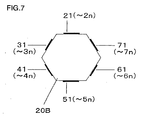
- FIG. 7 presents a referential example, not falling within the scope of the claims, of an LED mounting substrate assuming a hexagonal prism shape.
- FIG. 7 shows groups of blue LEDs, blue LEDs 21 to 2n, blue LEDs 31 to 3n, blue LEDs 41 to 4n, blue LEDs 51 to 5n, blue LEDs 61 to 6n and blue LEDs 71 to 7n, each mounted at one of the six surfaces of a substrate assembly 20B.
- the drive of the individual blue LEDs is controlled by a current supply circuit (not shown) so that they all emit light with a uniform level of light emission luminance.
- the substrate assembly 20B is used as a light emitter in place of the substrate 20 in the light emitting device shown in FIG. 5 .
- the blue component light can be invariably guided to the diffusion lens 3A reliably regardless of whether the blue component light is emitted toward the reflecting member 2 or toward the diffusion lens 3A.
- a light emission luminance twice that from a light emitting device with LEDs mounted at the two surfaces of a single substrate is achieved, whereas by mounting LEDs at the six surfaces of a hexagonal prism-shaped substrate assembly, a light emission luminance three times that of a light emitting device with LEDs mounted at the two surfaces of a single substrate, is achieved. In either case, a compact light emitting device with high luminance is achieved.
- the substrate assembly assuming a polygonal prism shape may be an octagonal prism assembly or a decagonal prism assembly.
- blue LEDs may be mounted on a polyhedron assembly achieved by combining surfaces including a curved surface, instead of a polygonal prism substrate assembly achieved by combining flat surfaces.
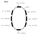
- groups of blue LEDs 21 to 2n, 31 to 3, 41 to 4n, 51 to 5n, 61 to 6n, 71 to 7n, 81 to 8n and 91 to 9n may be mounted at a flexible substrate 20C or the like constituted as a polyhedral body, as shown in FIG. 9 , so as to form LED arrays at a polyhedral substrate assuming any shape instead of a univocally defined shape such as a polygonal prism.
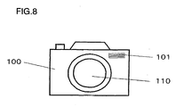
- FIG. 8 shows an interchangeable photographic lens 110 mounted at a camera body 100.
- An illuminating device 101 is provided as an internal unit in the camera body 100 at the upper right position, viewed from the subject side.
- the illuminating device 101 is constituted with the light emitting device explained earlier.
- the light emitting device may be utilized as a light source in a portable telephone equipped with a camera, a toy, a lighting device, a flashlight or the like, or as an illuminating device in a camera.
- LED light containing the blue component light is used as the photoluminescence primary light (excitation light) to obtain the yellow component light (secondary light)
- the wavelength component of the primary light and the wavelength component (color component) of the secondary light may be different from those in the example explained above.
- An optimal type of fluorescent material to be added into the material to constitute the Fresnel lens (or the diffusion lens) should be selected in correspondence to the specific purposes of use for the light emitting device, in conjunction with light emitting elements capable of emitting light with the optimal wavelength to be used as the excitation light source.
- LEDs that emit light with different color components may be mounted at the individual surfaces of the substrate assembly 20A or 20B assuming a polygonal prism shape in FIG. 6 or 7 .
- blue LEDs may be mounted at one surface
- red LEDs may be mounted at another surface
- green LEDs may be mounted at yet another surface.
- light can be emitted by selecting the optimal LEDs for light emission under specific circumstances.
- light emitting device adopting this structure, light containing the optimal color components for conditions can be obtained via the single light emitting device.
- a plurality of LEDs that emit light corresponding to a plurality of color components may be disposed at the substrate 1 shown in FIG. 1 .
- the color mixing ratio for the primary light and the secondary light should be adjusted by adjusting the content of the fluorescent material added into the material constituting the Fresnel lens 3 (or the diffusion lens 3A) or adjusting the thickness of the Fresnel lens 3 (or the diffusion lens 3A).
- the ratio of the secondary light is raised by increasing the content of the fluorescent material and the ratio of the secondary light can be lowered by reducing the fluorescent material content.
- the ratio of the secondary light can be raised by increasing the thickness of the Fresnel lens 3 (or the diffusion lens 3A) and the ratio of the secondary light can be lowered by reducing the thickness of the Fresnel lens 3 (or the diffusion lens 3A), without altering the fluorescent material content at all.
Landscapes
- Physics & Mathematics (AREA)
- General Physics & Mathematics (AREA)
- Led Device Packages (AREA)
- Non-Portable Lighting Devices Or Systems Thereof (AREA)
Claims (10)
- Beleuchtungsvorrichtung, umfassend:ein Substrat (20);ein Licht emittierendes Glied, das einen ersten Lichtemitter (21) umfasst, der direkt auf einer ersten Oberfläche des Substrats montiert ist, und einen zweiten Lichtemitter (31), der direkt auf einer zweiten Oberfläche, die eine Rückseite und direkt gegenüber der ersten Oberfläche ist, montiert ist, wobei der erste Lichtemitter und der zweite Lichtemitter Erregungslicht abgeben, das zum Erregen eines fluoreszierenden Materials verwendet wird;ein Reflexionsglied (2), das ein erstes, von dem ersten Lichtemitter abgegebenes Erregungslicht reflektiert; undein optisches Projektionsglied (3A), das das fluoreszierende Material enthält, das durch das erste Erregungslicht, das von dem ersten Lichtemitter abgegeben und dann an dem Reflexionsglied reflektiert wurde, und ein zweites, von dem zweiten Lichtemitter abgegebenes Erregungslicht erregt wird, um Photolumineszenzlicht zu erzeugen, wobei:das optische Projektionsglied weißes Licht, das durch Mischen des ersten Erregungslichts, des zweiten Erregungslichts und des Photolumineszenzlichts erhalten wird, projiziert.
- Beleuchtungsvorrichtung nach Anspruch 1, wobei:das erste, von dem ersten Lichtemitter (21) abgegebene Erregungslicht und das zweite, von dem zweiten Lichtemitter (31) abgegebene Erregungslicht jeweils eine blaue Farbkomponente enthalten; unddas von dem fluoreszierenden Material abgegebene Photolumineszenzlicht eine gelbe Farbkomponente enthält.
- Beleuchtungsvorrichtung nach Anspruch 2, wobei:das optische Projektionsglied (3A) aus Harz besteht, in das das fluoreszierende Material im Wesentlichen gleichförmig hinzugefügt wurde.
- Beleuchtungsvorrichtung nach einem der Ansprüche 1 bis 3, wobei:der erste Lichtemitter (21) und der zweite Lichtemitter (31) jeweils aus einer LED-Anordnung bestehen.
- Beleuchtungsvorrichtung nach Anspruch 4, wobei:der erste Lichtemitter (21) und der zweite Lichtemitter (31) Licht mit einem gleichförmigen Leuchtdichteniveau abgeben.
- Beleuchtungsvorrichtung nach einem der Ansprüche 1 bis 5, wobei:das Reflexionsglied (2) gebildet ist, um einen parabolischen Querschnitt zu haben.
- Beleuchtungsvorrichtung nach einem der Ansprüche 1 bis 6, wobei:das Projektionsglied (3A) eine Diffusionslinse ist.
- Beleuchtungsvorrichtung nach einem der Ansprüche 1 bis 7, wobei:das Substrat (20) ein flexibles Substrat ist.
- Beleuchtungsvorrichtung nach einem der Ansprüche 1 bis 8, wobei:der erste Lichtemitter (21) und der zweite Lichtemitter (31) Licht in verschiedenen Farben abgeben.
- Kamera, umfassend eine Beleuchtungsvorrichtung nach einem der Ansprüche 1 bis 9.
Applications Claiming Priority (2)
| Application Number | Priority Date | Filing Date | Title |
|---|---|---|---|
| JP2004318151A JP2006128562A (ja) | 2004-11-01 | 2004-11-01 | 発光装置 |
| PCT/JP2005/019921 WO2006049104A1 (ja) | 2004-11-01 | 2005-10-28 | 発光装置 |
Publications (3)
| Publication Number | Publication Date |
|---|---|
| EP1808640A1 EP1808640A1 (de) | 2007-07-18 |
| EP1808640A4 EP1808640A4 (de) | 2008-12-24 |
| EP1808640B1 true EP1808640B1 (de) | 2013-04-24 |
Family
ID=36319114
Family Applications (1)
| Application Number | Title | Priority Date | Filing Date |
|---|---|---|---|
| EP05805361.2A Not-in-force EP1808640B1 (de) | 2004-11-01 | 2005-10-28 | Lichtemittierende vorrichtung |
Country Status (5)
| Country | Link |
|---|---|
| US (1) | US7588339B2 (de) |
| EP (1) | EP1808640B1 (de) |
| JP (1) | JP2006128562A (de) |
| CN (1) | CN1993580B (de) |
| WO (1) | WO2006049104A1 (de) |
Families Citing this family (18)
| Publication number | Priority date | Publication date | Assignee | Title |
|---|---|---|---|---|
| US8374498B2 (en) * | 2006-09-29 | 2013-02-12 | Microscan Systems, Inc. | Systems and/or devices for camera-based inspections |
| US8032017B2 (en) * | 2006-09-29 | 2011-10-04 | Microscan Systems, Inc. | Methods for providing diffuse light |
| US7978970B2 (en) * | 2006-09-29 | 2011-07-12 | Microscan Systems, Inc. | Systems and/or devices for providing diffuse light |
| JP2010192582A (ja) * | 2009-02-17 | 2010-09-02 | Stanley Electric Co Ltd | Led発光装置 |
| CN101813297B (zh) * | 2009-02-24 | 2012-03-21 | 绎立锐光科技开发(深圳)有限公司 | 光源及其提供稳定出射光的方法 |
| TWM368029U (en) * | 2009-03-30 | 2009-11-01 | E Pin Internat Tech Co Ltd | Fresnel LED lens and LED assembly thereof |
| JP4756403B2 (ja) * | 2009-06-30 | 2011-08-24 | カシオ計算機株式会社 | 光源装置及びプロジェクタ |
| US8000594B2 (en) * | 2009-07-02 | 2011-08-16 | Microscan Systems, Inc. | Diffuse reflective illuminator |
| US8107808B2 (en) * | 2009-07-10 | 2012-01-31 | Microscan Systems, Inc. | Combination dark field and bright field illuminator |
| US8768159B2 (en) | 2009-07-10 | 2014-07-01 | Microscan Systems, Inc. | Combination dark field and bright field illuminator |
| EP2555261A1 (de) * | 2010-03-30 | 2013-02-06 | Mitsubishi Chemical Corporation | Lichtemittierende vorrichtung |
| JP5565065B2 (ja) * | 2010-04-21 | 2014-08-06 | コニカミノルタ株式会社 | 画像読み取り装置 |
| CN103375702A (zh) * | 2012-04-23 | 2013-10-30 | 展晶科技(深圳)有限公司 | Led发光装置 |
| US10203085B2 (en) * | 2015-05-29 | 2019-02-12 | Nichia Corporation | Light source device |
| US20180066810A1 (en) * | 2016-01-20 | 2018-03-08 | Telebrands Corp. | Illuminating apparatus |
| IL261148B2 (en) * | 2016-02-26 | 2023-12-01 | Magic Leap Inc | Light output system with reflector and lenses for high spatially uniform light output |
| EP4198627A4 (de) * | 2020-12-30 | 2024-03-27 | Hangzhou Hikvision Digital Technology Co., Ltd. | Lichtergänzende lampe für halbkugelförmige kamera und halbkugelförmige kamera |
| CN114321748A (zh) * | 2021-12-28 | 2022-04-12 | 林耀 | 白色光源装置 |
Family Cites Families (14)
| Publication number | Priority date | Publication date | Assignee | Title |
|---|---|---|---|---|
| JPS6022383Y2 (ja) * | 1980-03-04 | 1985-07-03 | 三洋電機株式会社 | 発光ダイオ−ド表示器 |
| JP3065550B2 (ja) * | 1997-01-20 | 2000-07-17 | 株式会社サンキデン | 多光源ランプ及びそのランプを用いた表示灯 |
| JP3639428B2 (ja) * | 1998-03-17 | 2005-04-20 | 三洋電機株式会社 | 光源装置 |
| DE69937993C5 (de) * | 1998-09-28 | 2019-01-10 | Koninklijke Philips N.V. | Beleuchtungsanordnung |
| JP2000133006A (ja) * | 1998-10-29 | 2000-05-12 | Sanyo Electric Co Ltd | 面光源 |
| US6504301B1 (en) | 1999-09-03 | 2003-01-07 | Lumileds Lighting, U.S., Llc | Non-incandescent lightbulb package using light emitting diodes |
| EP1328959A1 (de) | 2000-07-28 | 2003-07-23 | Osram Opto Semiconductors GmbH & Co. OHG | Auf lumineszenzumsetzung basierende leuchtdiode und leuchtstoffe für die wellenlängenumsetzung |
| JP2002134793A (ja) * | 2000-10-26 | 2002-05-10 | Omron Corp | 光素子用光学デバイス |
| JP3614776B2 (ja) * | 2000-12-19 | 2005-01-26 | シャープ株式会社 | チップ部品型ledとその製造方法 |
| JP2003100114A (ja) * | 2001-09-19 | 2003-04-04 | Koito Mfg Co Ltd | 車両用灯具 |
| JP2003141910A (ja) * | 2001-11-02 | 2003-05-16 | Stanley Electric Co Ltd | 車両用灯具 |
| JP2004039594A (ja) * | 2002-07-08 | 2004-02-05 | Seiwa Electric Mfg Co Ltd | 発光ダイオード素子を用いた照明器具 |
| JP2004226509A (ja) * | 2003-01-21 | 2004-08-12 | Fuji Photo Film Co Ltd | ストロボ装置及びカメラ |
| CN2646554Y (zh) | 2003-10-13 | 2004-10-06 | 璨圆光电股份有限公司 | 白光发光二极管灯具的发光装置 |
-
2004
- 2004-11-01 JP JP2004318151A patent/JP2006128562A/ja active Pending
-
2005
- 2005-10-28 CN CN2005800258135A patent/CN1993580B/zh not_active Expired - Fee Related
- 2005-10-28 EP EP05805361.2A patent/EP1808640B1/de not_active Not-in-force
- 2005-10-28 US US11/632,036 patent/US7588339B2/en not_active Expired - Fee Related
- 2005-10-28 WO PCT/JP2005/019921 patent/WO2006049104A1/ja active Application Filing
Also Published As
| Publication number | Publication date |
|---|---|
| EP1808640A4 (de) | 2008-12-24 |
| US20080158854A1 (en) | 2008-07-03 |
| CN1993580B (zh) | 2010-09-29 |
| EP1808640A1 (de) | 2007-07-18 |
| JP2006128562A (ja) | 2006-05-18 |
| WO2006049104A1 (ja) | 2006-05-11 |
| CN1993580A (zh) | 2007-07-04 |
| US7588339B2 (en) | 2009-09-15 |
Similar Documents
| Publication | Publication Date | Title |
|---|---|---|
| EP1808640B1 (de) | Lichtemittierende vorrichtung | |
| TWI430469B (zh) | 發光二極體燈源系統 | |
| JP4694567B2 (ja) | Led照明 | |
| TWI384182B (zh) | 燈組件 | |
| EP1794811B1 (de) | Beleuchtungssystem | |
| JP4861328B2 (ja) | 照明システム | |
| JP4792459B2 (ja) | 色混合のためのランプ及び反射器構成 | |
| EP1776722B1 (de) | Hochleistungs-led-lampen-system | |
| JP2002304903A (ja) | 照明器具 | |
| CA2577798A1 (en) | Optical system using led coupled with phosphor-doped reflective materials | |
| US20090046459A1 (en) | Lighting device | |
| JP5225799B2 (ja) | 照明装置 | |
| JP2518236B2 (ja) | 光源装置 | |
| KR101069693B1 (ko) | 측광원에 의해 발광하는 비구면렌즈를 이용한 엘이디 조명장치 | |
| WO2005106323A1 (en) | Variable colour lighting | |
| TWI263099B (en) | Backlight module | |
| CN213814255U (zh) | 一种三色led发光阵列结构 | |
| JPH01143367A (ja) | 多色led光源 | |
| JP2023004228A (ja) | 発光装置、面光源装置および表示装置 | |
| JP2015216014A (ja) | 光源モジュール | |
| TWM277003U (en) | Concentrating lens having the effect of uniform lights | |
| JPH0968936A (ja) | 発光ダイオードランプ |
Legal Events
| Date | Code | Title | Description |
|---|---|---|---|
| PUAI | Public reference made under article 153(3) epc to a published international application that has entered the european phase |
Free format text: ORIGINAL CODE: 0009012 |
|
| 17P | Request for examination filed |
Effective date: 20070126 |
|
| AK | Designated contracting states |
Kind code of ref document: A1 Designated state(s): AT BE BG CH CY CZ DE DK EE ES FI FR GB GR HU IE IS IT LI LT LU LV MC NL PL PT RO SE SI SK TR |
|
| DAX | Request for extension of the european patent (deleted) | ||
| A4 | Supplementary search report drawn up and despatched |
Effective date: 20081124 |
|
| RIC1 | Information provided on ipc code assigned before grant |
Ipc: F21V 9/08 20060101ALI20081118BHEP Ipc: F21K 7/00 20060101ALI20081118BHEP Ipc: H01L 33/00 20060101ALI20081118BHEP Ipc: F21Y 101/02 20060101ALN20081118BHEP Ipc: F21S 2/00 20060101AFI20061026BHEP |
|
| 17Q | First examination report despatched |
Effective date: 20090130 |
|
| RAP1 | Party data changed (applicant data changed or rights of an application transferred) |
Owner name: NIKON CORPORATION |
|
| REG | Reference to a national code |
Ref country code: DE Ref legal event code: R079 Ref document number: 602005039293 Country of ref document: DE Free format text: PREVIOUS MAIN CLASS: F21S0002000000 Ipc: F21K0099000000 |
|
| RIC1 | Information provided on ipc code assigned before grant |
Ipc: F21K 99/00 20100101AFI20110927BHEP Ipc: F21V 9/16 20060101ALI20110927BHEP |
|
| GRAP | Despatch of communication of intention to grant a patent |
Free format text: ORIGINAL CODE: EPIDOSNIGR1 |
|
| GRAS | Grant fee paid |
Free format text: ORIGINAL CODE: EPIDOSNIGR3 |
|
| GRAA | (expected) grant |
Free format text: ORIGINAL CODE: 0009210 |
|
| AK | Designated contracting states |
Kind code of ref document: B1 Designated state(s): AT BE BG CH CY CZ DE DK EE ES FI FR GB GR HU IE IS IT LI LT LU LV MC NL PL PT RO SE SI SK TR |
|
| REG | Reference to a national code |
Ref country code: GB Ref legal event code: FG4D |
|
| REG | Reference to a national code |
Ref country code: CH Ref legal event code: EP |
|
| REG | Reference to a national code |
Ref country code: AT Ref legal event code: REF Ref document number: 608831 Country of ref document: AT Kind code of ref document: T Effective date: 20130515 |
|
| REG | Reference to a national code |
Ref country code: IE Ref legal event code: FG4D |
|
| REG | Reference to a national code |
Ref country code: DE Ref legal event code: R096 Ref document number: 602005039293 Country of ref document: DE Effective date: 20130627 |
|
| REG | Reference to a national code |
Ref country code: AT Ref legal event code: MK05 Ref document number: 608831 Country of ref document: AT Kind code of ref document: T Effective date: 20130424 |
|
| REG | Reference to a national code |
Ref country code: LT Ref legal event code: MG4D |
|
| REG | Reference to a national code |
Ref country code: NL Ref legal event code: VDEP Effective date: 20130424 |
|
| PG25 | Lapsed in a contracting state [announced via postgrant information from national office to epo] |
Ref country code: IS Free format text: LAPSE BECAUSE OF FAILURE TO SUBMIT A TRANSLATION OF THE DESCRIPTION OR TO PAY THE FEE WITHIN THE PRESCRIBED TIME-LIMIT Effective date: 20130824 Ref country code: AT Free format text: LAPSE BECAUSE OF FAILURE TO SUBMIT A TRANSLATION OF THE DESCRIPTION OR TO PAY THE FEE WITHIN THE PRESCRIBED TIME-LIMIT Effective date: 20130424 Ref country code: BE Free format text: LAPSE BECAUSE OF FAILURE TO SUBMIT A TRANSLATION OF THE DESCRIPTION OR TO PAY THE FEE WITHIN THE PRESCRIBED TIME-LIMIT Effective date: 20130424 Ref country code: ES Free format text: LAPSE BECAUSE OF FAILURE TO SUBMIT A TRANSLATION OF THE DESCRIPTION OR TO PAY THE FEE WITHIN THE PRESCRIBED TIME-LIMIT Effective date: 20130804 Ref country code: LT Free format text: LAPSE BECAUSE OF FAILURE TO SUBMIT A TRANSLATION OF THE DESCRIPTION OR TO PAY THE FEE WITHIN THE PRESCRIBED TIME-LIMIT Effective date: 20130424 Ref country code: GR Free format text: LAPSE BECAUSE OF FAILURE TO SUBMIT A TRANSLATION OF THE DESCRIPTION OR TO PAY THE FEE WITHIN THE PRESCRIBED TIME-LIMIT Effective date: 20130725 Ref country code: SI Free format text: LAPSE BECAUSE OF FAILURE TO SUBMIT A TRANSLATION OF THE DESCRIPTION OR TO PAY THE FEE WITHIN THE PRESCRIBED TIME-LIMIT Effective date: 20130424 Ref country code: PT Free format text: LAPSE BECAUSE OF FAILURE TO SUBMIT A TRANSLATION OF THE DESCRIPTION OR TO PAY THE FEE WITHIN THE PRESCRIBED TIME-LIMIT Effective date: 20130826 Ref country code: SE Free format text: LAPSE BECAUSE OF FAILURE TO SUBMIT A TRANSLATION OF THE DESCRIPTION OR TO PAY THE FEE WITHIN THE PRESCRIBED TIME-LIMIT Effective date: 20130424 Ref country code: FI Free format text: LAPSE BECAUSE OF FAILURE TO SUBMIT A TRANSLATION OF THE DESCRIPTION OR TO PAY THE FEE WITHIN THE PRESCRIBED TIME-LIMIT Effective date: 20130424 |
|
| PG25 | Lapsed in a contracting state [announced via postgrant information from national office to epo] |
Ref country code: CY Free format text: LAPSE BECAUSE OF FAILURE TO SUBMIT A TRANSLATION OF THE DESCRIPTION OR TO PAY THE FEE WITHIN THE PRESCRIBED TIME-LIMIT Effective date: 20130424 Ref country code: PL Free format text: LAPSE BECAUSE OF FAILURE TO SUBMIT A TRANSLATION OF THE DESCRIPTION OR TO PAY THE FEE WITHIN THE PRESCRIBED TIME-LIMIT Effective date: 20130424 Ref country code: BG Free format text: LAPSE BECAUSE OF FAILURE TO SUBMIT A TRANSLATION OF THE DESCRIPTION OR TO PAY THE FEE WITHIN THE PRESCRIBED TIME-LIMIT Effective date: 20130724 Ref country code: LV Free format text: LAPSE BECAUSE OF FAILURE TO SUBMIT A TRANSLATION OF THE DESCRIPTION OR TO PAY THE FEE WITHIN THE PRESCRIBED TIME-LIMIT Effective date: 20130424 |
|
| PG25 | Lapsed in a contracting state [announced via postgrant information from national office to epo] |
Ref country code: SK Free format text: LAPSE BECAUSE OF FAILURE TO SUBMIT A TRANSLATION OF THE DESCRIPTION OR TO PAY THE FEE WITHIN THE PRESCRIBED TIME-LIMIT Effective date: 20130424 Ref country code: CZ Free format text: LAPSE BECAUSE OF FAILURE TO SUBMIT A TRANSLATION OF THE DESCRIPTION OR TO PAY THE FEE WITHIN THE PRESCRIBED TIME-LIMIT Effective date: 20130424 Ref country code: EE Free format text: LAPSE BECAUSE OF FAILURE TO SUBMIT A TRANSLATION OF THE DESCRIPTION OR TO PAY THE FEE WITHIN THE PRESCRIBED TIME-LIMIT Effective date: 20130424 Ref country code: DK Free format text: LAPSE BECAUSE OF FAILURE TO SUBMIT A TRANSLATION OF THE DESCRIPTION OR TO PAY THE FEE WITHIN THE PRESCRIBED TIME-LIMIT Effective date: 20130424 |
|
| PG25 | Lapsed in a contracting state [announced via postgrant information from national office to epo] |
Ref country code: RO Free format text: LAPSE BECAUSE OF FAILURE TO SUBMIT A TRANSLATION OF THE DESCRIPTION OR TO PAY THE FEE WITHIN THE PRESCRIBED TIME-LIMIT Effective date: 20130424 Ref country code: NL Free format text: LAPSE BECAUSE OF FAILURE TO SUBMIT A TRANSLATION OF THE DESCRIPTION OR TO PAY THE FEE WITHIN THE PRESCRIBED TIME-LIMIT Effective date: 20130424 Ref country code: IT Free format text: LAPSE BECAUSE OF FAILURE TO SUBMIT A TRANSLATION OF THE DESCRIPTION OR TO PAY THE FEE WITHIN THE PRESCRIBED TIME-LIMIT Effective date: 20130424 |
|
| PLBE | No opposition filed within time limit |
Free format text: ORIGINAL CODE: 0009261 |
|
| STAA | Information on the status of an ep patent application or granted ep patent |
Free format text: STATUS: NO OPPOSITION FILED WITHIN TIME LIMIT |
|
| 26N | No opposition filed |
Effective date: 20140127 |
|
| REG | Reference to a national code |
Ref country code: DE Ref legal event code: R097 Ref document number: 602005039293 Country of ref document: DE Effective date: 20140127 |
|
| PG25 | Lapsed in a contracting state [announced via postgrant information from national office to epo] |
Ref country code: MC Free format text: LAPSE BECAUSE OF FAILURE TO SUBMIT A TRANSLATION OF THE DESCRIPTION OR TO PAY THE FEE WITHIN THE PRESCRIBED TIME-LIMIT Effective date: 20130424 |
|
| REG | Reference to a national code |
Ref country code: CH Ref legal event code: PL |
|
| REG | Reference to a national code |
Ref country code: IE Ref legal event code: MM4A |
|
| PG25 | Lapsed in a contracting state [announced via postgrant information from national office to epo] |
Ref country code: CH Free format text: LAPSE BECAUSE OF NON-PAYMENT OF DUE FEES Effective date: 20131031 Ref country code: LI Free format text: LAPSE BECAUSE OF NON-PAYMENT OF DUE FEES Effective date: 20131031 |
|
| PG25 | Lapsed in a contracting state [announced via postgrant information from national office to epo] |
Ref country code: IE Free format text: LAPSE BECAUSE OF NON-PAYMENT OF DUE FEES Effective date: 20131028 |
|
| PGFP | Annual fee paid to national office [announced via postgrant information from national office to epo] |
Ref country code: FR Payment date: 20141008 Year of fee payment: 10 Ref country code: DE Payment date: 20141023 Year of fee payment: 10 Ref country code: GB Payment date: 20141022 Year of fee payment: 10 |
|
| PG25 | Lapsed in a contracting state [announced via postgrant information from national office to epo] |
Ref country code: TR Free format text: LAPSE BECAUSE OF FAILURE TO SUBMIT A TRANSLATION OF THE DESCRIPTION OR TO PAY THE FEE WITHIN THE PRESCRIBED TIME-LIMIT Effective date: 20130424 |
|
| PG25 | Lapsed in a contracting state [announced via postgrant information from national office to epo] |
Ref country code: HU Free format text: LAPSE BECAUSE OF FAILURE TO SUBMIT A TRANSLATION OF THE DESCRIPTION OR TO PAY THE FEE WITHIN THE PRESCRIBED TIME-LIMIT; INVALID AB INITIO Effective date: 20051028 Ref country code: LU Free format text: LAPSE BECAUSE OF NON-PAYMENT OF DUE FEES Effective date: 20131028 |
|
| REG | Reference to a national code |
Ref country code: DE Ref legal event code: R119 Ref document number: 602005039293 Country of ref document: DE |
|
| GBPC | Gb: european patent ceased through non-payment of renewal fee |
Effective date: 20151028 |
|
| PG25 | Lapsed in a contracting state [announced via postgrant information from national office to epo] |
Ref country code: GB Free format text: LAPSE BECAUSE OF NON-PAYMENT OF DUE FEES Effective date: 20151028 Ref country code: DE Free format text: LAPSE BECAUSE OF NON-PAYMENT OF DUE FEES Effective date: 20160503 |
|
| REG | Reference to a national code |
Ref country code: FR Ref legal event code: ST Effective date: 20160630 |
|
| PG25 | Lapsed in a contracting state [announced via postgrant information from national office to epo] |
Ref country code: FR Free format text: LAPSE BECAUSE OF NON-PAYMENT OF DUE FEES Effective date: 20151102 |