EP1794840B1 - Antennes planes pour des applications satellites mobiles - Google Patents
Antennes planes pour des applications satellites mobiles Download PDFInfo
- Publication number
- EP1794840B1 EP1794840B1 EP04787213A EP04787213A EP1794840B1 EP 1794840 B1 EP1794840 B1 EP 1794840B1 EP 04787213 A EP04787213 A EP 04787213A EP 04787213 A EP04787213 A EP 04787213A EP 1794840 B1 EP1794840 B1 EP 1794840B1
- Authority
- EP
- European Patent Office
- Prior art keywords
- radiating element
- ground plane
- patch
- antenna
- slots
- Prior art date
- Legal status (The legal status is an assumption and is not a legal conclusion. Google has not performed a legal analysis and makes no representation as to the accuracy of the status listed.)
- Active
Links
- 238000004891 communication Methods 0.000 claims abstract description 7
- 239000004033 plastic Substances 0.000 claims description 34
- 239000000758 substrate Substances 0.000 claims description 33
- 239000006260 foam Substances 0.000 claims description 23
- 239000004593 Epoxy Substances 0.000 claims description 21
- 229920001343 polytetrafluoroethylene Polymers 0.000 claims description 12
- 239000004810 polytetrafluoroethylene Substances 0.000 claims description 12
- 239000011800 void material Substances 0.000 claims description 4
- 238000010295 mobile communication Methods 0.000 claims description 3
- 230000005855 radiation Effects 0.000 description 22
- 239000002184 metal Substances 0.000 description 13
- 238000013461 design Methods 0.000 description 9
- 239000000463 material Substances 0.000 description 9
- 238000010168 coupling process Methods 0.000 description 6
- 238000005859 coupling reaction Methods 0.000 description 6
- 230000005284 excitation Effects 0.000 description 5
- 238000001465 metallisation Methods 0.000 description 5
- 230000005404 monopole Effects 0.000 description 5
- 230000001419 dependent effect Effects 0.000 description 4
- 230000008901 benefit Effects 0.000 description 3
- 230000008878 coupling Effects 0.000 description 3
- 238000011161 development Methods 0.000 description 2
- 230000009977 dual effect Effects 0.000 description 2
- 239000011521 glass Substances 0.000 description 2
- 239000000203 mixture Substances 0.000 description 2
- NJPPVKZQTLUDBO-UHFFFAOYSA-N novaluron Chemical compound C1=C(Cl)C(OC(F)(F)C(OC(F)(F)F)F)=CC=C1NC(=O)NC(=O)C1=C(F)C=CC=C1F NJPPVKZQTLUDBO-UHFFFAOYSA-N 0.000 description 2
- 230000010287 polarization Effects 0.000 description 2
- 238000005549 size reduction Methods 0.000 description 2
- MPCDNZSLJWJDNW-UHFFFAOYSA-N 1,2,3-trichloro-4-(3,5-dichlorophenyl)benzene Chemical compound ClC1=CC(Cl)=CC(C=2C(=C(Cl)C(Cl)=CC=2)Cl)=C1 MPCDNZSLJWJDNW-UHFFFAOYSA-N 0.000 description 1
- 238000013459 approach Methods 0.000 description 1
- 230000000712 assembly Effects 0.000 description 1
- 238000000429 assembly Methods 0.000 description 1
- 230000002457 bidirectional effect Effects 0.000 description 1
- 239000003990 capacitor Substances 0.000 description 1
- 239000002131 composite material Substances 0.000 description 1
- 230000003247 decreasing effect Effects 0.000 description 1
- 238000005530 etching Methods 0.000 description 1
- 238000004519 manufacturing process Methods 0.000 description 1
- 230000007246 mechanism Effects 0.000 description 1
- 238000000034 method Methods 0.000 description 1
- -1 polytetrafluoroethylene Polymers 0.000 description 1
- 230000008569 process Effects 0.000 description 1
Images


Classifications
-
- H—ELECTRICITY
- H01—ELECTRIC ELEMENTS
- H01Q—ANTENNAS, i.e. RADIO AERIALS
- H01Q9/00—Electrically-short antennas having dimensions not more than twice the operating wavelength and consisting of conductive active radiating elements
- H01Q9/04—Resonant antennas
- H01Q9/0407—Substantially flat resonant element parallel to ground plane, e.g. patch antenna
- H01Q9/045—Substantially flat resonant element parallel to ground plane, e.g. patch antenna with particular feeding means
- H01Q9/0457—Substantially flat resonant element parallel to ground plane, e.g. patch antenna with particular feeding means electromagnetically coupled to the feed line
-
- H—ELECTRICITY
- H01—ELECTRIC ELEMENTS
- H01Q—ANTENNAS, i.e. RADIO AERIALS
- H01Q1/00—Details of, or arrangements associated with, antennas
- H01Q1/27—Adaptation for use in or on movable bodies
- H01Q1/32—Adaptation for use in or on road or rail vehicles
- H01Q1/325—Adaptation for use in or on road or rail vehicles characterised by the location of the antenna on the vehicle
- H01Q1/3275—Adaptation for use in or on road or rail vehicles characterised by the location of the antenna on the vehicle mounted on a horizontal surface of the vehicle, e.g. on roof, hood, trunk
-
- H—ELECTRICITY
- H01—ELECTRIC ELEMENTS
- H01Q—ANTENNAS, i.e. RADIO AERIALS
- H01Q5/00—Arrangements for simultaneous operation of antennas on two or more different wavebands, e.g. dual-band or multi-band arrangements
- H01Q5/40—Imbricated or interleaved structures; Combined or electromagnetically coupled arrangements, e.g. comprising two or more non-connected fed radiating elements
-
- H—ELECTRICITY
- H01—ELECTRIC ELEMENTS
- H01Q—ANTENNAS, i.e. RADIO AERIALS
- H01Q9/00—Electrically-short antennas having dimensions not more than twice the operating wavelength and consisting of conductive active radiating elements
- H01Q9/04—Resonant antennas
- H01Q9/0407—Substantially flat resonant element parallel to ground plane, e.g. patch antenna
- H01Q9/0464—Annular ring patch
Definitions
- the invention relates generally to an antenna for vehicular mobile applications using mobile satellite systems, and more particularly, to a microstrip fed annular patch antenna with a conical radiation pattern with high directivity in the range of low elevation angle above the horizon.
- This kind of antenna is generally designed to be a car-top antenna for satellite communications.
- the invention also relates to a multi-system antenna.
- a solution consisting in using an omnidirectional antenna should not be envisaged due to low gain.
- Another solution consisting in using a phase array for tracking satellites should also not be envisaged as being too expensive for standard consumer terminals.
- Printed antennas are incontestably the best suited kind of antennas for the development of such front-ends circuits of an antenna for vehicular mobile applications.
- Typical user segment antennas for such applications can be subdivided in two main subsets: low and high latitudes.
- Low latitudes applications require antenna with a wide beam pointing in the vertical direction and their design does not present particular difficulties.
- geostationary satellites are seen at an elevation angle between 66° down to 22°.
- user antennas for mobile applications must have the maximum directivity at an elevation angle of approximately 45° and they must be omnidirectional in azimuth. In other words, these user antennas must have a conical radiation pattern.
- Printed antennas generating a conical radiation pattern are very interesting for the design of flat user terminal antennas for mobile satellite systems. Circular and annular patches resonating at higher modes are typical candidates to obtain such radiation patterns.
- the ring antenna comprises a metal resonant ring 101 tuned for the second-order mode (TM 21 ) of operation, which is fed by a metal feed post 103 and its series-connected capacitor 104.
- the ring antenna is dielectrically loaded to reduce its physical size by positioning a low-dielectric plastic or dielectric ring 107 under resonant ring 101.
- the monopole antenna comprises two metal posts 105 spaced on opposite sides of the central axis and supporting at their top end a metal disk 106. Mechanical support for feed post 103, metal monopole posts 105 and for a metal ground plane 109 is provided by a PCB 108.
- Both the ring antenna and the monopole antenna radiate in a conical radiation pattern, with the axis of the conical pattern extending generally perpendicular to the planar top surface of the antenna assembly 100 that contains both metal resonant ring 101 and metal disk 106.
- US Patent Application No. 2003/0210193 presents some drawbacks. Firstly, as it has been mentioned before, one of the most important requirement for user terminal antennas for mobile satellite communications is an antenna having a conical radiation pattern in the desired elevation angle, i.e. for instance between 20° and 60°, centered in the desired zone, for instance about 40-45°. In the antenna assembly presented in US Patent Application No. 2003/0210193 , both the ring antenna and the monopole antenna are excited via metal feed posts 103 and 105 which extend between the ground plane 109 and the corresponding radiating element 101 and 106.
- the main objects of the present invention are to overcome afore cited drawbacks by providing an antenna assembly with low-profile which can be arranged very close or even in contact to any kind of mobile support and which has a homogenous conical radiation pattern with a satisfactory efficiency.
- the present invention concerns an antenna assembly according to claim 1. Accordingly, a more homogenous conical radiation pattern is obtained with the feed line that provides signal energy in a contact less manner to or from the patch radiating element through the opening. Nevertheless, contact less coupling impedes use of a metal pedestal connecting with the first electrically ground plane. Therefore, it is further provided with the arrangement of an additional foam or air layer together with a second ground plane which strongly reduces influences due to the vehicle support on which the antenna assembly is embedded and also allows reducing the minimum required distance between the vehicle and the antenna assembly.
- Another object of the present invention relates to a flat multifunctional antenna system for vehicular terminals able to satisfy simultaneously the requirements of several mobile satellite system applications.
- the present invention also concerns a multi-system antenna assembly according to claim 14.
- the idea consists in particular to use the space left by the central part and/or the external periphery of the ring to integrate additional elements and hence access different systems without any increase in size and production cost.
- the antenna assembly is a microstrip patch antenna for mobile satellite communications resonating preferentially at second-order mode (TM 21 ) which resulting calculated radiation pattern is detailed in a publication entitled " Circularly polarized conical patterns from circular microstrip antennas" (IEEE Transactions and antennas propagation, vol. AP-32, No. 9, September 1984 ) enclosed herewith by way of reference.
- FIG. 1A is a cross section view of a simple antenna assembly according to a first embodiment of the present invention.
- antenna assembly 1 preferably occupies a thin disk-shaped or cylindrical volume having a central axis (D) and a height which can be divided into successive layers each being circular or ring-shaped.
- antenna assembly 1 comprises an annular patch radiating element 2, preferably printed or etched on an annular epoxy film forming a first layer L1 which secures patch radiating element 2 to the whole antenna assembly.
- Annular epoxy film L1 is glued on a first dielectric substrate layer L2 formed by a plastic material. Nevertheless, annular epoxy film L1 can be omitted and then patch radiating element 2 is directly glued on plastic layer L2.
- plastic layer L2 is ring-shaped, a disk-shaped void 3 being let in the middle. However as it will be described hereinafter in relation with Figures 9A-9B , this plastic layer L2 can have different shapes modifying its behaviour.
- first dielectric layer L2 there is a second dielectric layer L3 advantageously made of polytetrafluoroethylene, generally called PTFE.
- This second dielectric layer L3 is metallised on both faces.
- Upper metallic face 4, separating first dielectric layer L2 from second dielectric layer L3, is used as a first electrically conducting ground plane 4 for antenna assembly 1, and lower metallic face 5 is used to support the microstrip circuit of the antenna comprising lines 6, couplers (not shown), active elements (also not shown), etc...
- the different elements forming said microstrip circuit which design depends on the specific desired application, are well known for those skilled in the art and therefore will not be detailed herewith.
- Both metallic faces 4 and respectively, 5 can then be used to etch simultaneously at least one opening 7, advantageously a slot, and respectively, the microstrip circuit having in particular at least one microstrip or feed line 6.
- first dielectric layer L2 is arranged between opening 7 and patch radiating element 2 and that feeding line 6 provides signal energy in a contactless manner to or from patch radiating element 2 through opening 7.
- the assembly above-described forms a microstrip patch antenna for mobile satellite communications, which is design to be advantageously arranged in a car-top application.
- an antenna assembly 1 is strongly influenced by the car-top material and shape. Indeed, the behaviour of such an antenna assembly arranged directly on a car-top will be strongly different whether the car-top material is metal, glass or plastic and whether the car-top shape is plane or curved.
- a third dielectric layer L4 such as an air or a foam layer, under which is arranged a second ground plane 8 acting as a back shielding plate.
- Third dielectric layer L4 associated with second ground plane 8 enables to arrange the antenna assembly directly on the car-top or even embedded inside.
- Figure 1B is a top view of the simple antenna assembly according to the first embodiment shown on Figure 1A . Only some layers of the antenna of Figure 1A has been represented for sake of clarity.
- annular patch radiating element 2 which is supported by an epoxy film L1 arranged over first dielectric substrate L2 (not visible).
- first electrically conducting ground plane (not shown) has at least one opening 7 which is slot-shaped and which is at least partly facing annular patch radiating element 2.
- at least one feed line 6 is slot-coupled to annular patch radiating element 2.
- the electrically conducting ground plane preferably comprises two slots 7 and below two microstrip lines 6 which are fed through a hybrid coupler. Slots 7 are angularly shifted so as to obtain both left and right circular polarisations.
- Advantageously slots 7 are positioned along annular patch 2 forming an angle of 135° with regard the central axis (D). But both circular polarisations can also be obtained by positioning the two excitation slots with an angle of 45°, nevertheless the resulting conical beam will be less homogeneous, i.e.
- the slots are preferably etched on a circular ground plane. It is to be noted that a four slots variant is also possible. The extra two slots are then arranged symmetrically with respect to the central axis (D).
- this layer L2 is composed by a plastic ring or eventually disk made, for example, of 6 mm of plastic. On this plastic layer, can be glued an epoxy film L1 where the patch has been printed or etched.
- a long slot 7 is required to couple the energy from the microstrip line 6 to patch radiating element 2.
- the required size for a standard rectangular slot would be larger than the width of annular patch 2 that would increase the level of coupling between the excitation ports, i.e. the slots, and thus would decrease the circular polarisation quality.
- each slot 7 is folded up to be fully facing annular patch radiating element 2.
- Figures 10A-10C Some of the possible designs are shown on Figures 10A-10C .
- Dc dielectric constants
- the overall height or thickness of the antenna is very thin, but however the dielectric constant of the dielectric substrate, formed by layers L1 and L2, is greater than 2.
- Radiuses R 1 , R 2 , R 3 and R 4 which are shown on Figure 1B , correspond respectively to the outer radius of the ring dielectric layer (R 1 ), the outer radius of the annular patch (R 2 ), the inner radius of the annular patch (R 3 ), and the inner radius of the dielectric layer (R 4 ).
- Radius R i is the distance between the central axis and the middle point of the slots.
- the diameter is slightly greater than half the wavelength of the desired application.
- the diameter size of the antenna can be reduced of about 30% and the thickness of about 60%.
- the main advantage of this first preferred example is the very thin resulting height of the antenna, although it may be slightly less efficient than the following solutions described hereinafter in relation with the second and third embodiments.
- Figure 2 is a cross section view of a simple antenna assembly according to a first variant of a second embodiment of the present invention. All common elements with Figure 1A will not be described in detail again.
- the main difference between the previously described first embodiment and the second one relies on the dielectric substrate disposed between annular patch radiating element 2 and electrically conducting ground plane 4.
- the second embodiment it is provided with a dielectric substrate based on sandwiched dielectric layers L21 and L22 composed of materials with different characteristics.
- the ad-hoc composition of dielectric layers L21 and L22 with different permittivity and thickness allows to synthesize the permittivity of the dielectric substrate between annular patch 2 and first ground plane 4, and therefore to optimise the size of the antenna and its performances.
- the dielectric substrate is formed by a first layer L21 of plastic and a second layer L22 of foam or air. Then the resulting dielectric constant of this dielectric substrate can be adjusted to the desired value. For instance, it has been shown within the scope of the present invention, a more efficient antenna for a dielectric constant of the dielectric substrate being between 1 and 2. With a plastic layer having a dielectric constant larger than 2, and a foam layer having a dielectric constant near from 1, dielectric constants of the dielectric substrate between 1 and 2 can be obtained in varying the height of dielectric layers L21 and L22.
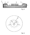
- Figure 5 is a schematic top view of Figures 2, 3 and 4 representing the slot arrangement towards the annular patch radiating element.
- the slots are arranged not right in the middle of the annular patch but are shifted to its inner periphery.
- the antenna matching may be adjusted by moving the slots along the annular patch. Nevertheless, it is important that both slots are kept with an angle of 135° in order to optimize reception of both circular polarisations.
- Radiuses R 1 and R 2 correspond to the outer, respectively to the inner radius of the annular patch. Radius R i corresponds to the average radius of the slots with respect to the central axis (D). Advantageously, radius R 2 is slightly greater than a quarter of the desired wavelength.
- FIG 3 is a cross section view of a simple antenna assembly according to a second variant of the second embodiment of the present invention. As for Figure 2 , only new elements of this antenna assembly will be detailed hereinafter.
- the first dielectric substrate disposed between annular patch radiating element 2 and electrically conducting ground plane 4.
- the first dielectric substrate is composed by three layers (L21-L23). Between slots 7 (only one being shown) etched in ground plane 4 and annular patch 2, there is a sandwich of one layer of foam L22 disposed between two layers L21 and L23 of epoxy or plastic.
- the annular patch is directly etched on a layer of plastic L21, but it can also be etched on a thin epoxy film.
- the antenna efficiency is increased for a dielectric constant of the dielectric substrate (L21-L23) being between 1 and 2.
- a dielectric constant can be obtained in varying the height of dielectric layers L21, L22 and L23.
- Dc dielectric constants
- the diameter size of the antenna can be reduced of about 20% and the thickness of about 45%.
- this multilayer dielectric substrate allows to optimize size reduction of the annular patch for low elevation angle and a wider radiation beam with respect to the previous one.
- An efficient experimental value for the dielectric constant is comprised between 1.7 and 1.9.
- FIG 4 is a cross section view of a simple antenna assembly according to a third variant of the second embodiment of the present invention.
- This third variant is still another variant of the first dielectric substrate disposed between annular patch radiating element 2 and electrically conducting ground plane 4.
- this dielectric substrate is provided with five layers (L21-L25) in order to obtain a dielectric substrate having an adjustable dielectric constant with the height of the different layers and whose behaviour is more homogenous in particular in term of radiation pattern.
- the annular patch is directly etched on a layer of plastic L21.
- Dc dielectric constants
- the antenna diameter is about 10% smaller and its thickness is about 30% less.
- this multilayer substrate allows having an annular patch size further optimized for low elevation angle and a wider radiation beam with respect to the previous one.
- An efficient experimental value for the dielectric constant is about 1.9.
- Figure 6 is a cross section view of a simple antenna assembly, the main difference with both first embodiments relies on the feeding means which are electromagnetically coupled to the annular patch instead of being slot-coupled.
- an annular patch radiating element 2 which is etched on a thin epoxy film (not shown, corresponding to L1 in the first embodiment) or directly on a plastic layer L21 of the first dielectric substrate.
- the first dielectric substrate comprises at least two layers (L21-L23).
- the dielectric substrate is formed by a sandwich of one epoxy or epoxy and foam layer L22 disposed between two layers of plastic L21 and L23.
- the first dielectric substrate we retrieve the second dielectric substrate L3, advantageously formed by a layer of PTFE.
- This PTFE layer is metallised on both faces 4 and 5, and it is used to etch on the bottom side the microstrip circuit (feeding lines, coupler, active elements, etc.).
- the metallization forms first electrically ground plane 4, in which at least one, and preferably two small circles 10 (only one shown) are etched to let passing through vertical metallic pins 11.
- Another feeding line 12 is etched in the intermediate epoxy layer L22 of the first dielectric substrate.
- Vertical metallic pins 11 are connected between feeding line 6 of the metallised bottom side of PTFE layer L3 and feeding line 12 embedded in the first dielectric substrate.
- the signal is electromagnetically coupled (no electric contact) between upper feeding line 12 and annular patch radiating element 2.
- a foam or air layer L4 is provided along with a second conducting ground plane 8 acting as a back shielding plate.
- the thickness and the diameter of this foam layer L4 can be reduced and consequently the overall size of the antenna can be also reduced.
- the efficiency of the antenna is then slightly decreased due to size reduction, but this loss is partially compensated by the fact that electromagnetio-coupled feeding is slightly more efficient than slot-coupled feeding.
- the posts are here well shorter and then do not affect the radiation pattern of the antenna.
- Dc dielectric constants
- electromagnetic-coupling is less influenced than slot-coupling by the support of the antenna (e.g. the car-top) and therefore the height of layer L4 could be further reduced.
- FIG. 7 is a partial top view of a first multi-system antenna assembly 21 according to any of the preceding embodiments of the present invention.
- this multi-system antenna it is provided with antennas for at least two applications and preferably more than two.
- a very interesting feature is the overall size of such a multi-system antenna which is about the same size as the mono-application antenna structure described hereinbefore. It is therefore very suitable for mobile communication systems which always require more functionalities and less space to implement these latter.
- the multi-system comprises a first antenna structure comprising an annular patch radiating element 22 slot-coupled, via slots 27, or electromagnetically-coupled (solution not shown on Figure 7 ) to feeding lines 26.
- this first antenna structure When used in the second-order resonant mode, this first antenna structure has a conical radiation pattern very useful and efficient for low elevation angle mobile satellite applications. It is reminded that the use of two slots 7 angularly shifted with an angle of 135° ensure a very efficient reception of both Right and Left Hand Circular Polarisations used by mobile satellite applications like WorldSpace.
- multi-system antenna assembly 21 further comprises at least a second antenna structure for receiving signals from another application or eventually signals coming from repeaters of the first desired application.
- the second antenna structure comprises a disk patch radiating element 33 being concentrically disposed, i.e. within the inner radius of the annular patch, and preferably coplanar with respect to annular patch 22, in a plane perpendicular to central axis (D) and is advantageously designed on the same substrate structure of the annular patch.
- This circular patch radiating element 33 is resonating at the fundamental mode.
- a second antenna microstrip circuit 35 is etched on the bottom side metallization of the PTFE layer and an opening, for example a slot 36, is etched on the upper side metallization facing disk patch radiating element 33.
- circular patch radiating element 33 is also fed through slots 36, 37 in the ground plane and is also dual circularly polarised to work with both Right Hand Circular Polarisation (RHCP) used by navigation systems like the Global Positioning System (GPS) and the future Galileo system, and Left Hand Circular Polarisation (LHCP) used by bidirectional mobile communication system like THURAYA.
- RHCP Right Hand Circular Polarisation
- GPS Global Positioning System
- LHCP Left Hand Circular Polarisation
- FIG 8 is a cross section of a second multi-system antenna assembly according to the first embodiment of the present invention.
- this second multi-system antenna assembly 41 in addition to first antenna patch radiating element 42 already described in relation with Figures 1A and 1B , it is further provided with at least one another antenna.
- a miniaturized GPS antenna 44 can be incorporated in void space 43 inside first ring-shaped dielectric substrate 45.
- a third antenna such as a radio FM antenna 46 is enrolled around the antenna assembly 41.
- Advantages of this solution are that both the GPS and the FM antennas are available at very low prices, and can be easily mounted on the microstrip patch antenna described in relation with the first embodiment.
- Figures 9A-9B show two possible shapes of the first dielectric substrate of the antenna assembly according to the first embodiment as well as the first mufti-system antenna assembly.
- dielectric layer L2 arranged between annular patch radiating element 2 and electrically conducting ground plane 4, wherein the opening is not shown.
- dielectric layer L2 is globally cylinder-shaped with at least one annular recess arranged at the cylinder periphery.
- dielectric layer L2 is frusto-conical shaped, the large base being arranged on the side of annular patch 2 and the small one being arranged on the side of ground plane 4.
- FIGS 10A-10C show different possible shapes of slots.
- it is very important that the whole surface covered by the slot faces completely the annular patch.
- Figure 10A shows a first example of a slot with an overturned H-shape.
- Figure 10B shows a second example of a slot which is C shaped.
- Figure 10C shows a third example of a slot with a mirrored T-shape.
- annular patches allow to design smaller antennas with respect to circular patches.
- the field density under the central part of the patch is very low.
- this part of the antenna can be cut out to obtain a ring without affecting the performances of the antenna; the cut portion can then be used for other applications.
- the electrical length of the antenna is increased, hence reducing the resonant frequency of the antenna.
Claims (18)
- Une antenne (1) à plaque en micro-ruban pour des communications par satellites mobiles comprenant:- un premier plan de masse (4) électriquement conducteur ayant deux fentes (7),- au moins un élément radiant (2) à plaque annulaire ayant un axe central (D),- au moins une première couche diélectrique (L2; L21-L22; L21-L23; L21-L25) disposée entre ledit premier plan de masse électriquement conducteur et ledit élément radiant à plaque et plus particulièrement entre lesdites fentes et ledit élément radiant à plaque,- deux lignes d'alimentation (6) couplées par une fente audit élément radiant à plaque pour fournir de l'énergie par signaux d'une manière sans contact audit ou dudit élément radiant à plaque à travers lesdites fentes et- une seconde couche diélectrique (L3) disposée entre ladite ligne d'alimentation et ledit premier plan de masse électriquement conducteur, pour laquelle l'antenne comprend en plus- un second plan de masse (8) et une troisième couche diélectrique (L4) disposée entre ledit second plan de masse et ladite ligne d'alimentation, et pour laquelle- lesdites deux fentes (7) sont orientées radialement par rapport à l'axe central et décalées angulairement de manière à recevoir deux polarisations circulaires gauche et droite.
- L'antenne à plaque en micro-ruban selon la revendication 1, pour laquelle lesdites fentes sont décalées angulairement de 135° par rapport à l'axe central (D).
- L'antenne à plaque en micro-ruban selon la revendication 1 ou 2, pour laquelle chacune desdites fentes est repliée pour être complètement en face dudit élément radiant à plaque annulaire, ladite fente étant préférablement de forme en C ou en T miroitée.
- L'antenne à plaque en micro-ruban selon l'une des revendications 1 à 3, pour laquelle l'antenne est substantiellement cylindrique et pour laquelle le rayon externe (R2) de l'élément radiant est légèrement plus grand qu'un quart de la longueur d'onde désirée.
- L'antenne à plaque en micro-ruban selon l'une des revendications 1 à 4, pour laquelle ladite première couche diélectrique a une section transversale géométrique annulaire définissant une région intérieure vide (3).
- L'antenne à plaque en micro-ruban selon l'une des revendications 1 à 5, pour laquelle ladite au moins première couche diélectrique est faite d'au moins une couche plastique, ladite seconde couche diélectrique étant faite de PTFE.
- L'antenne à plaque en micro-ruban selon l'une des revendications précédentes, pour laquelle une fine couche d'époxy (L1) est disposée entre ladite première couche diélectrique et ledit élément radiant à plaque.
- L'antenne à plaque en micro-ruban selon l'une des revendications 1 à 4, 6 ou 7, pour laquelle ladite première couche diélectrique est formée en tronc de cône, ayant une petite et une grande bases, ladite grande base étant agencée du côté de l'élément radiant à plaque et ladite petite base étant agencée du côté dudit premier plan de masse électriquement conducteur.
- L'antenne à plaque en micro-ruban selon l'une des revendications 1 à 4, 6 ou 7, pour laquelle ladite première couche diélectrique est de forme cylindrique avec au moins un logement annulaire agencé à la périphérie du cylindre.
- L'antenne à plaque en micro-ruban selon l'une des revendications 1 à 7, pour laquelle au moins deux couches diélectriques (L21-L22; L21-L23; L21-L25) sont disposées entre ledit premier plan de masse électriquement conducteur et ledit élément radiant à plaque, comprenant au moins une couche plastique (L21) et une couche de mousse (L22), et pour laquelle la constante diélectrique résultante de ces au moins deux couches est strictement plus grande que 1 et strictement moins grande que 2, et préférablement comprise entre 1.7 et 1.9.
- L'antenne à plaque en micro-ruban selon la revendication 10, pour laquelle trois couches diélectriques (L21-L23) sont disposées entre ledit premier plan de masse électriquement conducteur et ledit élément radiant à plaque, comprenant deux couches de plastique ou d'époxy (L21, L23) et une couche de mousse (L22) insérée entre lesdites couches de plastique ou d'époxy.
- L'antenne à plaque en micro-ruban selon la revendication 10, pour laquelle cinq couches diélectriques (L21-L25) sont disposées entre ledit premier plan de masse électriquement conducteur et ledit élément radiant à plaque, comprenant trois couches de plastique (L21, L23, L25) et deux couches de mousse (L22, L24) insérées entre lesdites couches plastiques.
- L'antenne à plaque en micro-ruban selon l'une des revendications précédentes, pour laquelle elle comprend en plus deux extra fentes, qui sont agencées symétriquement par rapport à l'axe central (D).
- Une antenne multi-système (21) pour des communications mobiles comprenant:- un premier plan de masse électriquement conducteur ayant deux premières (27) et une seconde (36, 37) fentes,- un élément radiant à plaque annulaire (22) et un élément radiant à plaque circulaire (33) agencé de manière concentrique et coplanaire par rapport audit élément radiant à plaque annulaire ayant un axe central (D),- au moins une première couche diélectrique disposée entre ledit plan de masse électriquement conducteur et lesdits éléments radiants à plaques annulaire et circulaire et plus particulièrement entre lesdites premières et seconde fentes et lesdits éléments radiants à plaques annulaire et circulaire,- deux premières (26) et une seconde (38) lignes d'alimentation couplées par une fente audit élément radiant à plaque pour fournir de l'énergie par signaux de manière sans contact auxdits ou desdits éléments radiants à plaques annulaire et circulaire respectivement à travers lesdites premières et seconde fentes,- une seconde couche diélectrique disposée entre lesdites premières et seconde lignes d'alimentation et ledit premier plan de masse électriquement conducteur et pour laquelle- lesdites deux premières fentes (27) sont orientées radialement par rapport à l'axe central et décalées angulairement de manière à recevoir deux polarisations circulaires gauche et droite d'une première application avec ledit élément radiant à plaque annulaire.
- L'antenne multi-système selon la revendication 14, pour laquelle elle comprend en plus un second plan de masse et une troisième couche diélectrique disposée entre ledit second plan de masse et lesdites lignes d'alimentation.
- L'antenne multi-système selon la revendication 14 ou 15, pour laquelle deux secondes fentes (36, 37) sont orientées tangentiellement et décalées angulairement de manière à recevoir une polarisation circulaire gauche, respectivement droite d'une seconde, respectivement troisième application.
- Une antenne multi-système comprenant une antenne à plaque en micro-ruban selon la revendication 5, pour laquelle elle comprend en plus une autre antenne disposée dans ladite région intérieure vide de l'antenne à plaque en micro-ruban.
- L'antenne multi-système selon la revendication 17, pour laquelle elle comprend en plus une troisième antenne formée par un substrat flexible enroulé autour de ladite antenne à plaque en micro-ruban.
Applications Claiming Priority (1)
| Application Number | Priority Date | Filing Date | Title |
|---|---|---|---|
| PCT/EP2004/052312 WO2006032305A1 (fr) | 2004-09-24 | 2004-09-24 | Antennes planes pour des applications satellites mobiles |
Publications (2)
| Publication Number | Publication Date |
|---|---|
| EP1794840A1 EP1794840A1 (fr) | 2007-06-13 |
| EP1794840B1 true EP1794840B1 (fr) | 2008-04-09 |
Family
ID=34958701
Family Applications (1)
| Application Number | Title | Priority Date | Filing Date |
|---|---|---|---|
| EP04787213A Active EP1794840B1 (fr) | 2004-09-24 | 2004-09-24 | Antennes planes pour des applications satellites mobiles |
Country Status (9)
| Country | Link |
|---|---|
| US (1) | US7667650B2 (fr) |
| EP (1) | EP1794840B1 (fr) |
| JP (1) | JP2008515253A (fr) |
| CN (1) | CN101065882B (fr) |
| AT (1) | ATE392029T1 (fr) |
| DE (1) | DE602004013054T2 (fr) |
| ES (1) | ES2307056T3 (fr) |
| HK (1) | HK1111525A1 (fr) |
| WO (1) | WO2006032305A1 (fr) |
Families Citing this family (32)
| Publication number | Priority date | Publication date | Assignee | Title |
|---|---|---|---|---|
| US8368596B2 (en) * | 2004-09-24 | 2013-02-05 | Viasat, Inc. | Planar antenna for mobile satellite applications |
| WO2007049376A1 (fr) * | 2005-10-27 | 2007-05-03 | Murata Manufacturing Co., Ltd. | Module haute frequence |
| US7973734B2 (en) * | 2007-10-31 | 2011-07-05 | Lockheed Martin Corporation | Apparatus and method for covering integrated antenna elements utilizing composite materials |
| US7696930B2 (en) * | 2008-04-14 | 2010-04-13 | International Business Machines Corporation | Radio frequency (RF) integrated circuit (IC) packages with integrated aperture-coupled patch antenna(s) in ring and/or offset cavities |
| KR100988909B1 (ko) | 2008-09-23 | 2010-10-20 | 한국전자통신연구원 | 고이득 및 광대역 특성을 갖는 마이크로스트립 패치 안테나 |
| US8130149B2 (en) * | 2008-10-24 | 2012-03-06 | Lockheed Martin Corporation | Wideband strip fed patch antenna |
| US8279137B2 (en) | 2008-11-13 | 2012-10-02 | Microsoft Corporation | Wireless antenna for emitting conical radiation |
| US9007265B2 (en) * | 2009-01-02 | 2015-04-14 | Polytechnic Institute Of New York University | Using dielectric substrates, embedded with vertical wire structures, with slotline and microstrip elements to eliminate parallel-plate or surface-wave radiation in printed-circuits, chip packages and antennas |
| US8319688B2 (en) * | 2009-02-18 | 2012-11-27 | Harris Corporation | Planar slot antenna having multi-polarization capability and associated methods |
| US8558740B2 (en) * | 2009-06-29 | 2013-10-15 | Viasat, Inc. | Hybrid single aperture inclined antenna |
| EP2312767A1 (fr) * | 2009-10-16 | 2011-04-20 | Astrium Limited | Demande de contenus de diffusion |
| KR101111668B1 (ko) * | 2010-08-27 | 2012-03-13 | 한국전자통신연구원 | 고이득 및 광대역 특성을 갖는 마이크로스트립 패치 안테나 |
| CN102694565A (zh) * | 2012-05-18 | 2012-09-26 | 西安电子科技大学 | 一种集成蛇形天线的3d-mcm射频系统 |
| CN104701610A (zh) * | 2014-08-11 | 2015-06-10 | 庄昆杰 | 具有控制波束宽度的小型化天线单元和大规模天线阵列 |
| CN104868236A (zh) * | 2015-04-16 | 2015-08-26 | 深圳市华信天线技术有限公司 | 抗载微带天线 |
| US9960493B2 (en) * | 2015-07-24 | 2018-05-01 | City University Of Hong Kong | Patch antenna |
| GB201513565D0 (en) * | 2015-07-30 | 2015-09-16 | Drayson Technologies Europ Ltd | Antenna |
| CN105406179B (zh) * | 2015-11-06 | 2018-08-21 | 中国电子科技集团公司第三十八研究所 | 一种高增益端射共形天线 |
| CN107196052A (zh) * | 2017-04-13 | 2017-09-22 | 成都电科星天科技有限公司 | 小尺寸低仰角全向辐射圆极化天线 |
| CN107196053A (zh) * | 2017-04-13 | 2017-09-22 | 成都电科星天科技有限公司 | 小尺寸低仰角全向辐射双圆极化天线 |
| WO2018202304A1 (fr) * | 2017-05-04 | 2018-11-08 | Huawei Technologies Co., Ltd. | Élément rayonnant à double polarisation et antenne |
| CN110832699B (zh) | 2017-09-12 | 2021-10-22 | 华为技术有限公司 | 双极化辐射元件和天线 |
| CN111602294B (zh) * | 2018-01-18 | 2023-09-05 | 株式会社村田制作所 | 带天线基板、以及天线模块 |
| WO2019142769A1 (fr) * | 2018-01-18 | 2019-07-25 | 株式会社村田製作所 | Substrat ayant une antenne fixée, et module d'antenne |
| JP2021530881A (ja) * | 2018-05-01 | 2021-11-11 | ウェハー エルエルシーWafer Llc | 低コストの電送用誘電体とそれを用いたアンテナ |
| KR102059277B1 (ko) * | 2018-12-11 | 2019-12-24 | 주식회사 기가레인 | 벤딩 신뢰성이 개선된 연성회로기판 및 이의 제조방법 |
| KR102059279B1 (ko) * | 2018-12-19 | 2019-12-24 | 주식회사 기가레인 | 차폐성이 향상된 벤딩부를 포함하는 연성회로기판 및 이의 제조방법 |
| CN113412557B (zh) * | 2019-02-08 | 2024-02-02 | 株式会社村田制作所 | 天线模块和通信装置 |
| KR102031203B1 (ko) * | 2019-03-20 | 2019-10-11 | 동우 화인켐 주식회사 | 안테나 적층체 및 이를 포함하는 화상 표시 장치 |
| CN112332115A (zh) * | 2020-10-28 | 2021-02-05 | 北京机电工程研究所 | 多模多功能通信导航共口径一体化天线 |
| CN112615146A (zh) * | 2020-11-20 | 2021-04-06 | 嘉兴佳利电子有限公司 | 一种小型化扁平天线性能优化的方法 |
| CN112688054A (zh) * | 2020-12-08 | 2021-04-20 | 武汉驷腾科技发展有限公司 | 一种高性能可穿戴ais天线 |
Family Cites Families (9)
| Publication number | Priority date | Publication date | Assignee | Title |
|---|---|---|---|---|
| US4843400A (en) * | 1988-08-09 | 1989-06-27 | Ford Aerospace Corporation | Aperture coupled circular polarization antenna |
| US5165109A (en) * | 1989-01-19 | 1992-11-17 | Trimble Navigation | Microwave communication antenna |
| US5210542A (en) | 1991-07-03 | 1993-05-11 | Ball Corporation | Microstrip patch antenna structure |
| JP3020777B2 (ja) * | 1993-07-23 | 2000-03-15 | 宏之 新井 | 二周波共用アンテナ |
| DE60120348T2 (de) * | 2001-03-05 | 2007-06-06 | Ericsson Ab | Schlitz-gekoppelte Antennenanordnung auf einem Mehrschicht-Substrat |
| US6597316B2 (en) * | 2001-09-17 | 2003-07-22 | The Mitre Corporation | Spatial null steering microstrip antenna array |
| JP3420232B2 (ja) * | 2001-11-16 | 2003-06-23 | 日本アンテナ株式会社 | 複合アンテナ |
| WO2003079488A2 (fr) * | 2002-03-15 | 2003-09-25 | The Board Of Trustees Of The Leland Stanford Junior University | Antenne a plaque microruban a deux elements permettant d'attenuer la perturbation radioelectrique |
| US6812902B2 (en) * | 2002-05-13 | 2004-11-02 | Centurion Wireless Technologies, Inc. | Low profile two-antenna assembly having a ring antenna and a concentrically-located monopole antenna |
-
2004
- 2004-09-24 EP EP04787213A patent/EP1794840B1/fr active Active
- 2004-09-24 CN CN200480044211XA patent/CN101065882B/zh not_active Expired - Fee Related
- 2004-09-24 AT AT04787213T patent/ATE392029T1/de not_active IP Right Cessation
- 2004-09-24 ES ES04787213T patent/ES2307056T3/es active Active
- 2004-09-24 JP JP2007532782A patent/JP2008515253A/ja active Pending
- 2004-09-24 US US11/575,654 patent/US7667650B2/en active Active
- 2004-09-24 DE DE602004013054T patent/DE602004013054T2/de active Active
- 2004-09-24 WO PCT/EP2004/052312 patent/WO2006032305A1/fr active Application Filing
-
2008
- 2008-02-21 HK HK08101871.4A patent/HK1111525A1/xx not_active IP Right Cessation
Also Published As
| Publication number | Publication date |
|---|---|
| US7667650B2 (en) | 2010-02-23 |
| JP2008515253A (ja) | 2008-05-08 |
| DE602004013054D1 (de) | 2008-05-21 |
| ATE392029T1 (de) | 2008-04-15 |
| WO2006032305A1 (fr) | 2006-03-30 |
| CN101065882A (zh) | 2007-10-31 |
| HK1111525A1 (en) | 2008-08-08 |
| CN101065882B (zh) | 2010-12-01 |
| US20080266178A1 (en) | 2008-10-30 |
| ES2307056T3 (es) | 2008-11-16 |
| DE602004013054T2 (de) | 2009-05-07 |
| EP1794840A1 (fr) | 2007-06-13 |
Similar Documents
| Publication | Publication Date | Title |
|---|---|---|
| EP1794840B1 (fr) | Antennes planes pour des applications satellites mobiles | |
| US8368596B2 (en) | Planar antenna for mobile satellite applications | |
| US6646618B2 (en) | Low-profile slot antenna for vehicular communications and methods of making and designing same | |
| US6812902B2 (en) | Low profile two-antenna assembly having a ring antenna and a concentrically-located monopole antenna | |
| US5099249A (en) | Microstrip antenna for vehicular satellite communications | |
| US6697019B1 (en) | Low-profile dual-antenna system | |
| US7042403B2 (en) | Dual band, low profile omnidirectional antenna | |
| EP0907983B1 (fr) | Antenne reseau plane bifrequence | |
| US6480162B2 (en) | Low cost compact omini-directional printed antenna | |
| JP3020777B2 (ja) | 二周波共用アンテナ | |
| EP1118138B1 (fr) | Antenne resonante dielectrique a polarisation circulaire | |
| US6700539B2 (en) | Dielectric-patch resonator antenna | |
| US6664932B2 (en) | Multifunction antenna for wireless and telematic applications | |
| US9240631B2 (en) | Reduced ground plane shorted-patch hemispherical omni antenna | |
| US6859181B2 (en) | Integrated spiral and top-loaded monopole antenna | |
| EP1616368A1 (fr) | Systeme d'antenne pour un vehicule automobile | |
| JP2001168637A (ja) | クロスダイポールアンテナ | |
| WO1996035241A1 (fr) | Unite d'antenne | |
| CN219658967U (zh) | 交叉偶极子天线及天线阵 | |
| KR20070083615A (ko) | 이동 위성 애플리케이션을 위한 평면 안테나 | |
| JP2004048367A (ja) | 複合アンテナ | |
| JP2001332927A (ja) | 多周波フラフープ形アンテナ | |
| GB2411524A (en) | Dual slot cavity antenna with slots of differing resonant frequencies | |
| Licul et al. | 1. Markets Reviewing SDARS Antenna Requirements Sept. 1, 2003 Several conflicting requirements, such as achieving two separate high-gain antenna patterns within a single compact module, increase the challenge of designing SDARS antennas. | |
| Shafai et al. | Antenna candidates for digital radio broadcast |
Legal Events
| Date | Code | Title | Description |
|---|---|---|---|
| PUAI | Public reference made under article 153(3) epc to a published international application that has entered the european phase |
Free format text: ORIGINAL CODE: 0009012 |
|
| 17P | Request for examination filed |
Effective date: 20070424 |
|
| AK | Designated contracting states |
Kind code of ref document: A1 Designated state(s): AT BE BG CH CY CZ DE DK EE ES FI FR GB GR HU IE IT LI LU MC NL PL PT RO SE SI SK TR |
|
| AX | Request for extension of the european patent |
Extension state: AL HR LT LV MK |
|
| GRAP | Despatch of communication of intention to grant a patent |
Free format text: ORIGINAL CODE: EPIDOSNIGR1 |
|
| GRAS | Grant fee paid |
Free format text: ORIGINAL CODE: EPIDOSNIGR3 |
|
| GRAA | (expected) grant |
Free format text: ORIGINAL CODE: 0009210 |
|
| AK | Designated contracting states |
Kind code of ref document: B1 Designated state(s): AT BE BG CH CY CZ DE DK EE ES FI FR GB GR HU IE IT LI LU MC NL PL PT RO SE SI SK TR |
|
| AX | Request for extension of the european patent |
Extension state: AL HR LT LV MK |
|
| RAP1 | Party data changed (applicant data changed or rights of an application transferred) |
Owner name: JAST SA |
|
| REG | Reference to a national code |
Ref country code: GB Ref legal event code: FG4D |
|
| REG | Reference to a national code |
Ref country code: CH Ref legal event code: EP |
|
| REG | Reference to a national code |
Ref country code: IE Ref legal event code: FG4D |
|
| REF | Corresponds to: |
Ref document number: 602004013054 Country of ref document: DE Date of ref document: 20080521 Kind code of ref document: P |
|
| REG | Reference to a national code |
Ref country code: SE Ref legal event code: TRGR |
|
| REG | Reference to a national code |
Ref country code: CH Ref legal event code: NV Representative=s name: ICB INGENIEURS CONSEILS EN BREVETS SA |
|
| LTIE | Lt: invalidation of european patent or patent extension |
Effective date: 20080409 |
|
| PG25 | Lapsed in a contracting state [announced via postgrant information from national office to epo] |
Ref country code: SI Free format text: LAPSE BECAUSE OF FAILURE TO SUBMIT A TRANSLATION OF THE DESCRIPTION OR TO PAY THE FEE WITHIN THE PRESCRIBED TIME-LIMIT Effective date: 20080409 |
|
| NLV1 | Nl: lapsed or annulled due to failure to fulfill the requirements of art. 29p and 29m of the patents act | ||
| PG25 | Lapsed in a contracting state [announced via postgrant information from national office to epo] |
Ref country code: FI Free format text: LAPSE BECAUSE OF FAILURE TO SUBMIT A TRANSLATION OF THE DESCRIPTION OR TO PAY THE FEE WITHIN THE PRESCRIBED TIME-LIMIT Effective date: 20080409 Ref country code: BG Free format text: LAPSE BECAUSE OF FAILURE TO SUBMIT A TRANSLATION OF THE DESCRIPTION OR TO PAY THE FEE WITHIN THE PRESCRIBED TIME-LIMIT Effective date: 20080709 Ref country code: NL Free format text: LAPSE BECAUSE OF FAILURE TO SUBMIT A TRANSLATION OF THE DESCRIPTION OR TO PAY THE FEE WITHIN THE PRESCRIBED TIME-LIMIT Effective date: 20080409 Ref country code: PT Free format text: LAPSE BECAUSE OF FAILURE TO SUBMIT A TRANSLATION OF THE DESCRIPTION OR TO PAY THE FEE WITHIN THE PRESCRIBED TIME-LIMIT Effective date: 20080911 |
|
| REG | Reference to a national code |
Ref country code: ES Ref legal event code: FG2A Ref document number: 2307056 Country of ref document: ES Kind code of ref document: T3 |
|
| PG25 | Lapsed in a contracting state [announced via postgrant information from national office to epo] |
Ref country code: PL Free format text: LAPSE BECAUSE OF FAILURE TO SUBMIT A TRANSLATION OF THE DESCRIPTION OR TO PAY THE FEE WITHIN THE PRESCRIBED TIME-LIMIT Effective date: 20080409 Ref country code: AT Free format text: LAPSE BECAUSE OF FAILURE TO SUBMIT A TRANSLATION OF THE DESCRIPTION OR TO PAY THE FEE WITHIN THE PRESCRIBED TIME-LIMIT Effective date: 20080409 |
|
| ET | Fr: translation filed | ||
| PG25 | Lapsed in a contracting state [announced via postgrant information from national office to epo] |
Ref country code: CZ Free format text: LAPSE BECAUSE OF FAILURE TO SUBMIT A TRANSLATION OF THE DESCRIPTION OR TO PAY THE FEE WITHIN THE PRESCRIBED TIME-LIMIT Effective date: 20080409 Ref country code: DK Free format text: LAPSE BECAUSE OF FAILURE TO SUBMIT A TRANSLATION OF THE DESCRIPTION OR TO PAY THE FEE WITHIN THE PRESCRIBED TIME-LIMIT Effective date: 20080409 |
|
| PLBE | No opposition filed within time limit |
Free format text: ORIGINAL CODE: 0009261 |
|
| STAA | Information on the status of an ep patent application or granted ep patent |
Free format text: STATUS: NO OPPOSITION FILED WITHIN TIME LIMIT |
|
| PG25 | Lapsed in a contracting state [announced via postgrant information from national office to epo] |
Ref country code: BE Free format text: LAPSE BECAUSE OF FAILURE TO SUBMIT A TRANSLATION OF THE DESCRIPTION OR TO PAY THE FEE WITHIN THE PRESCRIBED TIME-LIMIT Effective date: 20080409 Ref country code: SK Free format text: LAPSE BECAUSE OF FAILURE TO SUBMIT A TRANSLATION OF THE DESCRIPTION OR TO PAY THE FEE WITHIN THE PRESCRIBED TIME-LIMIT Effective date: 20080409 Ref country code: RO Free format text: LAPSE BECAUSE OF FAILURE TO SUBMIT A TRANSLATION OF THE DESCRIPTION OR TO PAY THE FEE WITHIN THE PRESCRIBED TIME-LIMIT Effective date: 20080409 |
|
| 26N | No opposition filed |
Effective date: 20090112 |
|
| PG25 | Lapsed in a contracting state [announced via postgrant information from national office to epo] |
Ref country code: MC Free format text: LAPSE BECAUSE OF NON-PAYMENT OF DUE FEES Effective date: 20080930 Ref country code: EE Free format text: LAPSE BECAUSE OF FAILURE TO SUBMIT A TRANSLATION OF THE DESCRIPTION OR TO PAY THE FEE WITHIN THE PRESCRIBED TIME-LIMIT Effective date: 20080409 |
|
| PG25 | Lapsed in a contracting state [announced via postgrant information from national office to epo] |
Ref country code: IE Free format text: LAPSE BECAUSE OF NON-PAYMENT OF DUE FEES Effective date: 20080924 |
|
| PG25 | Lapsed in a contracting state [announced via postgrant information from national office to epo] |
Ref country code: CY Free format text: LAPSE BECAUSE OF FAILURE TO SUBMIT A TRANSLATION OF THE DESCRIPTION OR TO PAY THE FEE WITHIN THE PRESCRIBED TIME-LIMIT Effective date: 20080409 |
|
| PG25 | Lapsed in a contracting state [announced via postgrant information from national office to epo] |
Ref country code: HU Free format text: LAPSE BECAUSE OF FAILURE TO SUBMIT A TRANSLATION OF THE DESCRIPTION OR TO PAY THE FEE WITHIN THE PRESCRIBED TIME-LIMIT Effective date: 20081010 Ref country code: LU Free format text: LAPSE BECAUSE OF NON-PAYMENT OF DUE FEES Effective date: 20080924 |
|
| PG25 | Lapsed in a contracting state [announced via postgrant information from national office to epo] |
Ref country code: TR Free format text: LAPSE BECAUSE OF FAILURE TO SUBMIT A TRANSLATION OF THE DESCRIPTION OR TO PAY THE FEE WITHIN THE PRESCRIBED TIME-LIMIT Effective date: 20080409 |
|
| PG25 | Lapsed in a contracting state [announced via postgrant information from national office to epo] |
Ref country code: GR Free format text: LAPSE BECAUSE OF FAILURE TO SUBMIT A TRANSLATION OF THE DESCRIPTION OR TO PAY THE FEE WITHIN THE PRESCRIBED TIME-LIMIT Effective date: 20080710 |
|
| REG | Reference to a national code |
Ref country code: FR Ref legal event code: PLFP Year of fee payment: 12 |
|
| PGFP | Annual fee paid to national office [announced via postgrant information from national office to epo] |
Ref country code: GB Payment date: 20150825 Year of fee payment: 12 Ref country code: CH Payment date: 20150824 Year of fee payment: 12 Ref country code: DE Payment date: 20150820 Year of fee payment: 12 Ref country code: ES Payment date: 20150911 Year of fee payment: 12 |
|
| PGFP | Annual fee paid to national office [announced via postgrant information from national office to epo] |
Ref country code: FR Payment date: 20150824 Year of fee payment: 12 Ref country code: SE Payment date: 20150820 Year of fee payment: 12 |
|
| PGFP | Annual fee paid to national office [announced via postgrant information from national office to epo] |
Ref country code: IT Payment date: 20150828 Year of fee payment: 12 |
|
| REG | Reference to a national code |
Ref country code: DE Ref legal event code: R119 Ref document number: 602004013054 Country of ref document: DE |
|
| PG25 | Lapsed in a contracting state [announced via postgrant information from national office to epo] |
Ref country code: SE Free format text: LAPSE BECAUSE OF NON-PAYMENT OF DUE FEES Effective date: 20160925 |
|
| REG | Reference to a national code |
Ref country code: CH Ref legal event code: PL |
|
| REG | Reference to a national code |
Ref country code: SE Ref legal event code: EUG |
|
| GBPC | Gb: european patent ceased through non-payment of renewal fee |
Effective date: 20160924 |
|
| REG | Reference to a national code |
Ref country code: FR Ref legal event code: ST Effective date: 20170531 |
|
| PG25 | Lapsed in a contracting state [announced via postgrant information from national office to epo] |
Ref country code: GB Free format text: LAPSE BECAUSE OF NON-PAYMENT OF DUE FEES Effective date: 20160924 Ref country code: LI Free format text: LAPSE BECAUSE OF NON-PAYMENT OF DUE FEES Effective date: 20160930 Ref country code: DE Free format text: LAPSE BECAUSE OF NON-PAYMENT OF DUE FEES Effective date: 20170401 Ref country code: FR Free format text: LAPSE BECAUSE OF NON-PAYMENT OF DUE FEES Effective date: 20160930 Ref country code: CH Free format text: LAPSE BECAUSE OF NON-PAYMENT OF DUE FEES Effective date: 20160930 |
|
| PG25 | Lapsed in a contracting state [announced via postgrant information from national office to epo] |
Ref country code: IT Free format text: LAPSE BECAUSE OF NON-PAYMENT OF DUE FEES Effective date: 20160924 |
|
| PG25 | Lapsed in a contracting state [announced via postgrant information from national office to epo] |
Ref country code: ES Free format text: LAPSE BECAUSE OF NON-PAYMENT OF DUE FEES Effective date: 20160925 |
|
| REG | Reference to a national code |
Ref country code: ES Ref legal event code: FD2A Effective date: 20181126 |
|
| P01 | Opt-out of the competence of the unified patent court (upc) registered |
Effective date: 20230529 |