EP1793426A2 - Semiconductor device having a via hole and its manufacturing method - Google Patents
Semiconductor device having a via hole and its manufacturing method Download PDFInfo
- Publication number
- EP1793426A2 EP1793426A2 EP06023940A EP06023940A EP1793426A2 EP 1793426 A2 EP1793426 A2 EP 1793426A2 EP 06023940 A EP06023940 A EP 06023940A EP 06023940 A EP06023940 A EP 06023940A EP 1793426 A2 EP1793426 A2 EP 1793426A2
- Authority
- EP
- European Patent Office
- Prior art keywords
- electrode
- front surface
- via hole
- transistor
- semiconductor device
- Prior art date
- Legal status (The legal status is an assumption and is not a legal conclusion. Google has not performed a legal analysis and makes no representation as to the accuracy of the status listed.)
- Withdrawn
Links
Images


Classifications
-
- H—ELECTRICITY
- H10—SEMICONDUCTOR DEVICES; ELECTRIC SOLID-STATE DEVICES NOT OTHERWISE PROVIDED FOR
- H10D—INORGANIC ELECTRIC SEMICONDUCTOR DEVICES
- H10D30/00—Field-effect transistors [FET]
- H10D30/60—Insulated-gate field-effect transistors [IGFET]
- H10D30/64—Double-diffused metal-oxide semiconductor [DMOS] FETs
- H10D30/66—Vertical DMOS [VDMOS] FETs
- H10D30/663—Vertical DMOS [VDMOS] FETs having both source contacts and drain contacts on the same surface, i.e. up-drain VDMOS
-
- H—ELECTRICITY
- H10—SEMICONDUCTOR DEVICES; ELECTRIC SOLID-STATE DEVICES NOT OTHERWISE PROVIDED FOR
- H10D—INORGANIC ELECTRIC SEMICONDUCTOR DEVICES
- H10D30/00—Field-effect transistors [FET]
- H10D30/01—Manufacture or treatment
- H10D30/021—Manufacture or treatment of FETs having insulated gates [IGFET]
- H10D30/028—Manufacture or treatment of FETs having insulated gates [IGFET] of double-diffused metal oxide semiconductor [DMOS] FETs
- H10D30/0291—Manufacture or treatment of FETs having insulated gates [IGFET] of double-diffused metal oxide semiconductor [DMOS] FETs of vertical DMOS [VDMOS] FETs
- H10D30/0297—Manufacture or treatment of FETs having insulated gates [IGFET] of double-diffused metal oxide semiconductor [DMOS] FETs of vertical DMOS [VDMOS] FETs using recessing of the gate electrodes, e.g. to form trench gate electrodes
-
- H—ELECTRICITY
- H10—SEMICONDUCTOR DEVICES; ELECTRIC SOLID-STATE DEVICES NOT OTHERWISE PROVIDED FOR
- H10D—INORGANIC ELECTRIC SEMICONDUCTOR DEVICES
- H10D30/00—Field-effect transistors [FET]
- H10D30/60—Insulated-gate field-effect transistors [IGFET]
- H10D30/64—Double-diffused metal-oxide semiconductor [DMOS] FETs
- H10D30/66—Vertical DMOS [VDMOS] FETs
- H10D30/668—Vertical DMOS [VDMOS] FETs having trench gate electrodes, e.g. UMOS transistors
-
- H—ELECTRICITY
- H10—SEMICONDUCTOR DEVICES; ELECTRIC SOLID-STATE DEVICES NOT OTHERWISE PROVIDED FOR
- H10D—INORGANIC ELECTRIC SEMICONDUCTOR DEVICES
- H10D62/00—Semiconductor bodies, or regions thereof, of devices having potential barriers
- H10D62/10—Shapes, relative sizes or dispositions of the regions of the semiconductor bodies; Shapes of the semiconductor bodies
- H10D62/13—Semiconductor regions connected to electrodes carrying current to be rectified, amplified or switched, e.g. source or drain regions
- H10D62/149—Source or drain regions of field-effect devices
- H10D62/151—Source or drain regions of field-effect devices of IGFETs
- H10D62/156—Drain regions of DMOS transistors
- H10D62/159—Shapes
-
- H—ELECTRICITY
- H10—SEMICONDUCTOR DEVICES; ELECTRIC SOLID-STATE DEVICES NOT OTHERWISE PROVIDED FOR
- H10D—INORGANIC ELECTRIC SEMICONDUCTOR DEVICES
- H10D64/00—Electrodes of devices having potential barriers
- H10D64/20—Electrodes characterised by their shapes, relative sizes or dispositions
- H10D64/23—Electrodes carrying the current to be rectified, amplified, oscillated or switched, e.g. sources, drains, anodes or cathodes
- H10D64/251—Source or drain electrodes for field-effect devices
- H10D64/252—Source or drain electrodes for field-effect devices for vertical or pseudo-vertical devices
-
- H—ELECTRICITY
- H10—SEMICONDUCTOR DEVICES; ELECTRIC SOLID-STATE DEVICES NOT OTHERWISE PROVIDED FOR
- H10D—INORGANIC ELECTRIC SEMICONDUCTOR DEVICES
- H10D64/00—Electrodes of devices having potential barriers
- H10D64/20—Electrodes characterised by their shapes, relative sizes or dispositions
- H10D64/23—Electrodes carrying the current to be rectified, amplified, oscillated or switched, e.g. sources, drains, anodes or cathodes
- H10D64/251—Source or drain electrodes for field-effect devices
- H10D64/252—Source or drain electrodes for field-effect devices for vertical or pseudo-vertical devices
- H10D64/2523—Source or drain electrodes for field-effect devices for vertical or pseudo-vertical devices for vertical devices wherein the source or drain electrodes extend entirely through semiconductor bodies
-
- H—ELECTRICITY
- H10—SEMICONDUCTOR DEVICES; ELECTRIC SOLID-STATE DEVICES NOT OTHERWISE PROVIDED FOR
- H10D—INORGANIC ELECTRIC SEMICONDUCTOR DEVICES
- H10D64/00—Electrodes of devices having potential barriers
- H10D64/20—Electrodes characterised by their shapes, relative sizes or dispositions
- H10D64/23—Electrodes carrying the current to be rectified, amplified, oscillated or switched, e.g. sources, drains, anodes or cathodes
- H10D64/251—Source or drain electrodes for field-effect devices
- H10D64/256—Source or drain electrodes for field-effect devices for lateral devices wherein the source or drain electrodes are recessed in semiconductor bodies
-
- H—ELECTRICITY
- H10—SEMICONDUCTOR DEVICES; ELECTRIC SOLID-STATE DEVICES NOT OTHERWISE PROVIDED FOR
- H10W—GENERIC PACKAGES, INTERCONNECTIONS, CONNECTORS OR OTHER CONSTRUCTIONAL DETAILS OF DEVICES COVERED BY CLASS H10
- H10W20/00—Interconnections in chips, wafers or substrates
- H10W20/20—Interconnections within wafers or substrates, e.g. through-silicon vias [TSV]
-
- H—ELECTRICITY
- H10—SEMICONDUCTOR DEVICES; ELECTRIC SOLID-STATE DEVICES NOT OTHERWISE PROVIDED FOR
- H10D—INORGANIC ELECTRIC SEMICONDUCTOR DEVICES
- H10D62/00—Semiconductor bodies, or regions thereof, of devices having potential barriers
- H10D62/10—Shapes, relative sizes or dispositions of the regions of the semiconductor bodies; Shapes of the semiconductor bodies
- H10D62/117—Shapes of semiconductor bodies
-
- H—ELECTRICITY
- H10—SEMICONDUCTOR DEVICES; ELECTRIC SOLID-STATE DEVICES NOT OTHERWISE PROVIDED FOR
- H10W—GENERIC PACKAGES, INTERCONNECTIONS, CONNECTORS OR OTHER CONSTRUCTIONAL DETAILS OF DEVICES COVERED BY CLASS H10
- H10W72/00—Interconnections or connectors in packages
- H10W72/071—Connecting or disconnecting
- H10W72/072—Connecting or disconnecting of bump connectors
- H10W72/07251—Connecting or disconnecting of bump connectors characterised by changes in properties of the bump connectors during connecting
-
- H—ELECTRICITY
- H10—SEMICONDUCTOR DEVICES; ELECTRIC SOLID-STATE DEVICES NOT OTHERWISE PROVIDED FOR
- H10W—GENERIC PACKAGES, INTERCONNECTIONS, CONNECTORS OR OTHER CONSTRUCTIONAL DETAILS OF DEVICES COVERED BY CLASS H10
- H10W72/00—Interconnections or connectors in packages
- H10W72/20—Bump connectors, e.g. solder bumps or copper pillars; Dummy bumps; Thermal bumps
Definitions
- the present invention relates to a semiconductor device comprising at least one first electrode provided on the front surface of a semiconductor chip and electrically connected to at least one of electrodes that constitute a transistor, and a second electrode provided on the back surface of a semiconductor chip and electrically connected to one of the other electrodes, and its manufacturing method. More particularly it relates to a flip chip packaging technique of a power semiconductor device comprising a power MOSFET.
- the power MOSFET is a power device widely used in various kinds of power supply circuits and a car and the like, and improvement of its performance such as high-speed switching, lowering of on-resistance and the like have been demanded.
- the power MOSFET mainly comprises a trench type (vertical type) and a planar type (lateral type) and the trench type power MOSFET especially has a structure suitable for realizing high voltage resistance, large current intensity and low on-resistance, and it is an optimal element as a switching element.
- flip chip packaging In order to address the demand to high density chip wirings, attentions have been focused on flip chip packaging recently as an optimal packaging technique to implement function aggregation on a single chip that has been promoted by an electronics industry. With the flip chip method, a wire inductance can be considerably reduced and cost can be reduced because a die can be miniaturized.
- the flip chip packaging since connection is made only from the front surface of the chip, the flip chip packaging cannot be used for a trench type power MOSFET or a planar type power MOSFET in which the source electrode is formed on the front surface of the chip and the drain electrode is formed on the back surface thereof, for example, because the drain region on the back surface cannot be connected to a pad.
- a trench type power MOSFET structure of a semiconductor device having the drain region on the back surface that can employ the flip chip packaging by connecting the drain region from the front surface for example, Flip chip Power MOSFET : A New Wafer Scale Packaging Technique (ISPSD, June 2001) that is referred to as the document hereinafter.
- a diffusion layer that is the same type as the drain region is formed from the front surface to the drain region on the back surface so that the drain region on the back surface of the chip can be connected from the front surface, whereby the flip chip packaging can be employed.
- the diffusion layer that is the same type as the drain region is formed so that it can be connected from the front surface through a substrate, the resistance of the drain region becomes high, which leads to the increase in on-resistance that is an important parameter in the power device. As a result, the characteristics of the element deteriorate.
- the present invention was made in view of the above problem and it is an object of the present invention to provide a semiconductor device in which a through electrode is formed from the front surface to the back surface of a chip and this through electrode is connected to a metal layer connected to a drain region formed on the back surface to minimize the increase in resistance of the drain region, whereby the flip chip packaging can be employed.
- the semiconductor device of the present invention having the above characteristics is further characterized in that the transistor is a trench type power MOSFET, at least one of the first electrodes is electrically connected to the source electrode of the transistor, and the through electrode is electrically connected to the drain electrode of the transistor through the second electrode.
- the semiconductor device according to the present invention having the first characteristics is further characterized in that the transistor is a planar type power MOSFET, at least one of the first electrodes is electrically connected to the source electrode of the transistor, and the through electrode is electrically connected to the drain electrode of the transistor through the second electrode.
- the semiconductor device according to the present invention having any one of the above characteristics is further characterized in that a part of the through electrode exposed on the front surface of the semiconductor chip and the first electrode are used as terminals for external connection when the semiconductor chip is packaged.
- a manufacturing method of a semiconductor device according to the present invention to attain the above object is for manufacturing the semiconductor device according to the present invention having any one of the above characteristics and it is characterized by comprising forming the via hole so as to reach the second electrode from the front surface of a semiconductor substrate on which the transistor and the second electrode are formed and forming the through electrode by filling the via hole by a plating process.
- the manufacturing method of the semiconductor device according to the present invention having the above characteristics is further characterized by comprising plating the whole front surface of the semiconductor substrate by the plating process and patterning the plating by etching so that the through electrode and the first electrode are patterned at the same time.
- the manufacturing method of the semiconductor device according to the present invention having any one of the above characteristics further characterized by comprising depositing a seed metal film at least on the inner wall of the via hole before the plating process.
- the flip chip packaging can be employed even in the semiconductor device in which the source electrode is formed on the front surface of the semiconductor chip and a drain electrode formed on the back surface thereof.
- a wired can be considerably shortened, a wiring inductance can be reduced, and the performance of an element such as switching characteristics can be improved, and furthermore, a power supply noise can be considerably reduced.
- the flip chip packaging does not need an outer peripheral space in a bonding pad, the chip size can be miniaturized and costs can be reduced.
- the concrete manufacturing method of the above semiconductor device can be provided.
- the semiconductor device can employ the flip chip packaging even when the semiconductor device comprises the source electrode on the front surface of the semiconductor chip and the drain electrode on the back surface thereof, and a working effect of the semiconductor device described above can be provided.
- Fig. 1 is a schematic sectional view showing the schematic constitution of the device of the present invention according to this embodiment.
- a transistor used in this embodiment is a trench type power MOSFET and at least one first electrode 11b provided on the front surface of a silicon substrate 1 is electrically connected to the source electrode of the transistor through a metal wiring 5.
- a through electrode 11a is electrically connected to the drain electrode of the transistor through a second electrode (metal layer 9) provided on the back surface of the silicon substrate 1.
- the through electrode 11a is electrically connected to the second electrode (metal layer 9) through a via hole that penetrates a semiconductor chip from its front surface to its back surface.
- a part of the through electrode 11a exposed on the front surface of the semiconductor chip and the first electrode 11b are used as terminals for external connection when the semiconductor chip is packaged.
- a gate electrode (polysilicon layer 6) is electrically connected to one of the other first electrodes 11b on the front surface of the silicon substrate 1 although it is not shown.
- an epitaxial layer 2, an interlayer insulating film 3, a passivation film 4, the metal wiring 5, the polysilicon layer 6, a channel region 7 and a drift region 8 are formed on the silicon substrate 1 through conventional processes to form a trench type power MOSFET.
- a resist is applied to the back surface of the silicon substrate 1 and aligned by a both-side aligner that can align the back surface based on an alignment mark on the front surface such that the back surface of the silicon substrate 1 in the region of the trench type power MOSFET is opened, and then patterned.
- the silicon substrate 1 is etched away by a dry etching technique and the like to thin the thickness of the silicon substrate 1 to about 100 ⁇ m in the device area indicated as X.
- the metal layer 9 is formed on the back surface of the silicon substrate 1 by sputtering.
- the material of the metal layer 9 is not particularly limited, it is preferable that a metal material having low resistance is used to minimize the increase in on-resistance.
- a via hole 10 is formed so as to reach the metal layer 9 from the front surface of the silicon substrate 1 so that the metal layer 9 formed on the back surface of the silicon substrate 1 (the drain region of the trench type power MOSFET) can be connected from the front surface of the silicon substrate 1. More specifically, the via hole 10 is formed by applying a resist on the front surface of the silicon substrate 1 and patterning the via hole 10 having a diameter of about 20 ⁇ m ⁇ using a conventional photo technique. Then, the interlayer insulating film 3, the epitaxial layer 2 and the silicon substrate 1 are etched away by dry etching, whereby the via hole 10 reaches the metal layer 9 sputtered on the back surface of the silicon substrate 1.
- the through electrode 11a is formed by filling the via hole 10 with a plating material by a plating process with gold (Au), nickel (Ni) and the like. Furthermore, here, before the plating process, a seed metal film is deposited at least on the inner wall of the via hole 10. More specifically, after a seed metal (metal having a two-layer structure of Au/Ti) as a seed metal film has been deposited on the inner wall of the via hole 10 by sputtering, the plating process is performed on the whole front surface of the silicon substrate 1 to form a plating 11 so that the via hole 10 is filled with the plating 11. As the plating material, gold (Au), nickel (Ni) or the like is used.
- a resist is applied to the front surface of the silicon substrate 1 to pattern the front surface of the silicon substrate 1 so that a part other than the plating 11 that will be connected to a carrier at the time of flip chip packaging is opened, and the plating 11 and the seed metal film are etched away at the same time.
- the through electrode 11a is formed and the metal layer 9 formed on the back surface of the silicon substrate 1 can be connected from the front surface of the silicon substrate 1.
- the trench type power MOSFET is formed by the conventional processes similar to the first embodiment. Then, according to this embodiment, as shown in Fig. 3A, the thickness of a silicon substrate 1 is thinned to about 100 ⁇ m by grinding the back surface.
- a metal layer 9 is formed on the back surface of the silicon substrate 1 by sputtering.
- the material of the metal layer 9 is not particularly limited similar to the first embodiment, a metal material having low resistance is used to minimize the increase in on-resistance.
- a via hole 10 is formed so as to reach the metal layer 9 from the front surface of the silicon substrate 1 so that the metal layer 9 formed on the back surface of the silicon substrate 1 (the drain region of the trench type power MOSFET) can be connected from the front surface of the silicon substrate 1. More specifically, the via hole 10 is formed by applying a resist on the front surface of the silicon substrate 1 and patterning the via hole 10 having a diameter of about 20 ⁇ m ⁇ using a conventional photo technique similar to the embodiment 1. Then, the interlayer insulating film 3, the epitaxial layer 2 and the silicon substrate 1 are etched away by dry etching, whereby the via hole 10 reaches the metal layer 9 sputtered on the back surface of the silicon substrate 1.
- the via hole 10 is filled with a plating material and the plating material is deposited on the whole front surface of the silicon substrate 1 by the plating process with gold (Au), nickel (Ni) and the like.
- gold (Au), nickel (Ni) or the like is used similar to the first embodiment.
- a resist is applied to the front surface of the silicon substrate 1 to pattern the front surface of the silicon substrate 1 so that a part other than the plating 11 that will be connected to a carrier at the time of flip chip packaging is opened, and the plating 11 and the seed metal film are etched away at the same time.
- the through electrode 11a is formed and the metal layer 9 formed on the back surface of the silicon substrate 1 can be connected from the front surface of the silicon substrate 1.
- the device of the present invention and the method of the present invention may be applied to a semiconductor device in which a transistor is a planar type power MOSFET.
- the device of the present invention and the method of the present invention may be applied to an insulated gate type bipolar transistor (IGBT), for example, other than the power MOSFET.
- IGBT insulated gate type bipolar transistor
Landscapes
- Internal Circuitry In Semiconductor Integrated Circuit Devices (AREA)
- Electrodes Of Semiconductors (AREA)
- Insulated Gate Type Field-Effect Transistor (AREA)
Abstract
Description
- The present invention relates to a semiconductor device comprising at least one first electrode provided on the front surface of a semiconductor chip and electrically connected to at least one of electrodes that constitute a transistor, and a second electrode provided on the back surface of a semiconductor chip and electrically connected to one of the other electrodes, and its manufacturing method. More particularly it relates to a flip chip packaging technique of a power semiconductor device comprising a power MOSFET.
- The power MOSFET is a power device widely used in various kinds of power supply circuits and a car and the like, and improvement of its performance such as high-speed switching, lowering of on-resistance and the like have been demanded. The power MOSFET mainly comprises a trench type (vertical type) and a planar type (lateral type) and the trench type power MOSFET especially has a structure suitable for realizing high voltage resistance, large current intensity and low on-resistance, and it is an optimal element as a switching element.
- In order to address the demand to high density chip wirings, attentions have been focused on flip chip packaging recently as an optimal packaging technique to implement function aggregation on a single chip that has been promoted by an electronics industry. With the flip chip method, a wire inductance can be considerably reduced and cost can be reduced because a die can be miniaturized. However, according to the flip chip packaging, since connection is made only from the front surface of the chip, the flip chip packaging cannot be used for a trench type power MOSFET or a planar type power MOSFET in which the source electrode is formed on the front surface of the chip and the drain electrode is formed on the back surface thereof, for example, because the drain region on the back surface cannot be connected to a pad.
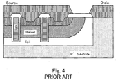
- Meanwhile, as shown in Fig. 4, there is disclosed a trench type power MOSFET structure of a semiconductor device having the drain region on the back surface that can employ the flip chip packaging by connecting the drain region from the front surface (for example, Flip chip Power MOSFET : A New Wafer Scale Packaging Technique (ISPSD, June 2001) that is referred to as the document hereinafter). According to this semiconductor device, a diffusion layer that is the same type as the drain region is formed from the front surface to the drain region on the back surface so that the drain region on the back surface of the chip can be connected from the front surface, whereby the flip chip packaging can be employed.
- However, according to the structure of the semiconductor device disclosed in the document, since the diffusion layer that is the same type as the drain region is formed so that it can be connected from the front surface through a substrate, the resistance of the drain region becomes high, which leads to the increase in on-resistance that is an important parameter in the power device. As a result, the characteristics of the element deteriorate.
- The present invention was made in view of the above problem and it is an object of the present invention to provide a semiconductor device in which a through electrode is formed from the front surface to the back surface of a chip and this through electrode is connected to a metal layer connected to a drain region formed on the back surface to minimize the increase in resistance of the drain region, whereby the flip chip packaging can be employed. In addition, it is an object of the present invention to provide a manufacturing method of the semiconductor device that can employ the flip chip packaging.
- A semiconductor device according to the present invention to attain the above object comprises at least one first electrode provided on the front surface of a semiconductor chip and electrically connected to at least one of electrodes that constitute a transistor, and a second electrode provided on the back surface of the semiconductor chip and electrically connected to one of the other electrodes, and it is characterized by having a via hole penetrating the semiconductor chip from the front surface to the back surface and a through electrode a part of which is exposed on the front surface of the semiconductor chip electrically connected to the second electrode through the via hole, as the first characteristics.
- The semiconductor device of the present invention having the above characteristics is further characterized in that the transistor is a trench type power MOSFET, at least one of the first electrodes is electrically connected to the source electrode of the transistor, and the through electrode is electrically connected to the drain electrode of the transistor through the second electrode.
- The semiconductor device according to the present invention having the first characteristics is further characterized in that the transistor is a planar type power MOSFET, at least one of the first electrodes is electrically connected to the source electrode of the transistor, and the through electrode is electrically connected to the drain electrode of the transistor through the second electrode.
- The semiconductor device according to the present invention having any one of the above characteristics is further characterized in that a part of the through electrode exposed on the front surface of the semiconductor chip and the first electrode are used as terminals for external connection when the semiconductor chip is packaged.
- A manufacturing method of a semiconductor device according to the present invention to attain the above object is for manufacturing the semiconductor device according to the present invention having any one of the above characteristics and it is characterized by comprising forming the via hole so as to reach the second electrode from the front surface of a semiconductor substrate on which the transistor and the second electrode are formed and forming the through electrode by filling the via hole by a plating process.
- The manufacturing method of the semiconductor device according to the present invention having the above characteristics is further characterized by comprising plating the whole front surface of the semiconductor substrate by the plating process and patterning the plating by etching so that the through electrode and the first electrode are patterned at the same time.
- The manufacturing method of the semiconductor device according to the present invention having any one of the above characteristics further characterized by comprising depositing a seed metal film at least on the inner wall of the via hole before the plating process.
- According to the semiconductor device in the present invention, since the through electrode that is electrically connected to the second electrode through the via hole that penetrates the semiconductor chip from the front surface to the back surface is provided, the flip chip packaging can be employed even in the semiconductor device in which the source electrode is formed on the front surface of the semiconductor chip and a drain electrode formed on the back surface thereof. Thus, as compared with the conventional packaging, a wired can be considerably shortened, a wiring inductance can be reduced, and the performance of an element such as switching characteristics can be improved, and furthermore, a power supply noise can be considerably reduced. In addition, since the flip chip packaging does not need an outer peripheral space in a bonding pad, the chip size can be miniaturized and costs can be reduced.
- In addition, according to the manufacturing method of the semiconductor device in the present invention, the concrete manufacturing method of the above semiconductor device can be provided. As a result, the semiconductor device can employ the flip chip packaging even when the semiconductor device comprises the source electrode on the front surface of the semiconductor chip and the drain electrode on the back surface thereof, and a working effect of the semiconductor device described above can be provided.
-
- Fig. 1 is a schematic sectional view showing a schematic constitution of a semiconductor device according to a first embodiment of the present invention;
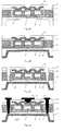
- Figs. 2A to 2D are sectional views showing the steps of a manufacturing method of the semiconductor device according to the first embodiment of the present invention;
- Figs. 3A to 3D are sectional views showing the steps of a manufacturing method of the semiconductor device according to a second embodiment of the present invention;
- Fig. 4 is a schematic sectional view showing a schematic constitution of a semiconductor device according to a conventional technique; and
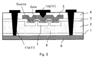
- Fig. 5 is a schematic sectional view showing a schematic constitution of a semiconductor device according to another embodiment of the present invention.
- Embodiments of a semiconductor device and its manufacturing method according to the present invention (referred to as the "device of the present invention" and "method of the present invention" occasionally) will be described with reference to the drawings hereinafter.
- The device of the present invention and the method of the present invention according to a first embodiment will be described with reference to Fig. 1 and Figs. 2A to 2D. Here, Fig. 1 is a schematic sectional view showing the schematic constitution of the device of the present invention according to this embodiment.
- A transistor used in this embodiment is a trench type power MOSFET and at least one
first electrode 11b provided on the front surface of asilicon substrate 1 is electrically connected to the source electrode of the transistor through ametal wiring 5. In addition, athrough electrode 11a is electrically connected to the drain electrode of the transistor through a second electrode (metal layer 9) provided on the back surface of thesilicon substrate 1. Furthermore, the throughelectrode 11a is electrically connected to the second electrode (metal layer 9) through a via hole that penetrates a semiconductor chip from its front surface to its back surface. A part of thethrough electrode 11a exposed on the front surface of the semiconductor chip and thefirst electrode 11b are used as terminals for external connection when the semiconductor chip is packaged. In addition, a gate electrode (polysilicon layer 6) is electrically connected to one of the otherfirst electrodes 11b on the front surface of thesilicon substrate 1 although it is not shown. - The method of the present invention according to this embodiment will be described with reference to Figs. 2A to 2D hereinafter.
- First, an
epitaxial layer 2, an interlayerinsulating film 3, apassivation film 4, themetal wiring 5, thepolysilicon layer 6, achannel region 7 and adrift region 8 are formed on thesilicon substrate 1 through conventional processes to form a trench type power MOSFET. Then, a resist is applied to the back surface of thesilicon substrate 1 and aligned by a both-side aligner that can align the back surface based on an alignment mark on the front surface such that the back surface of thesilicon substrate 1 in the region of the trench type power MOSFET is opened, and then patterned. Then, as shown in Fig. 2A, thesilicon substrate 1 is etched away by a dry etching technique and the like to thin the thickness of thesilicon substrate 1 to about 100µm in the device area indicated as X. - Then, as shown in Fig. 2B, the
metal layer 9 is formed on the back surface of thesilicon substrate 1 by sputtering. At this time, although the material of themetal layer 9 is not particularly limited, it is preferable that a metal material having low resistance is used to minimize the increase in on-resistance. - Then, as shown in Fig. 2C, a
via hole 10 is formed so as to reach themetal layer 9 from the front surface of thesilicon substrate 1 so that themetal layer 9 formed on the back surface of the silicon substrate 1 (the drain region of the trench type power MOSFET) can be connected from the front surface of thesilicon substrate 1. More specifically, thevia hole 10 is formed by applying a resist on the front surface of thesilicon substrate 1 and patterning thevia hole 10 having a diameter of about 20µmϕ using a conventional photo technique. Then, theinterlayer insulating film 3, theepitaxial layer 2 and thesilicon substrate 1 are etched away by dry etching, whereby thevia hole 10 reaches themetal layer 9 sputtered on the back surface of thesilicon substrate 1. - Then, as shown in Fig. 2D, the
through electrode 11a is formed by filling thevia hole 10 with a plating material by a plating process with gold (Au), nickel (Ni) and the like. Furthermore, here, before the plating process, a seed metal film is deposited at least on the inner wall of thevia hole 10. More specifically, after a seed metal (metal having a two-layer structure of Au/Ti) as a seed metal film has been deposited on the inner wall of the viahole 10 by sputtering, the plating process is performed on the whole front surface of thesilicon substrate 1 to form aplating 11 so that the viahole 10 is filled with theplating 11. As the plating material, gold (Au), nickel (Ni) or the like is used. Then, a resist is applied to the front surface of thesilicon substrate 1 to pattern the front surface of thesilicon substrate 1 so that a part other than the plating 11 that will be connected to a carrier at the time of flip chip packaging is opened, and theplating 11 and the seed metal film are etched away at the same time. Thus, the throughelectrode 11a is formed and themetal layer 9 formed on the back surface of thesilicon substrate 1 can be connected from the front surface of thesilicon substrate 1. - The method of the present invention according to a second embodiment will be described with reference to Figs. 3A to 3D. In this embodiment, a description will be made, taking the trench type power MOSFET as an example similar to the first embodiment.
- First, the trench type power MOSFET is formed by the conventional processes similar to the first embodiment. Then, according to this embodiment, as shown in Fig. 3A, the thickness of a
silicon substrate 1 is thinned to about 100µm by grinding the back surface. - Then, as shown in Fig. 3B, a
metal layer 9 is formed on the back surface of thesilicon substrate 1 by sputtering. In this embodiment, although the material of themetal layer 9 is not particularly limited similar to the first embodiment, a metal material having low resistance is used to minimize the increase in on-resistance. - Then, as shown in Fig. 3C, a via
hole 10 is formed so as to reach themetal layer 9 from the front surface of thesilicon substrate 1 so that themetal layer 9 formed on the back surface of the silicon substrate 1 (the drain region of the trench type power MOSFET) can be connected from the front surface of thesilicon substrate 1. More specifically, the viahole 10 is formed by applying a resist on the front surface of thesilicon substrate 1 and patterning the viahole 10 having a diameter of about 20µmϕ using a conventional photo technique similar to theembodiment 1. Then, theinterlayer insulating film 3, theepitaxial layer 2 and thesilicon substrate 1 are etched away by dry etching, whereby the viahole 10 reaches themetal layer 9 sputtered on the back surface of thesilicon substrate 1. - Then, as shown in Fig. 3D, after a seed metal (Au/Ti) as a seed metal film has been deposited on the inner wall of the via
hole 10 by sputtering, the viahole 10 is filled with a plating material and the plating material is deposited on the whole front surface of thesilicon substrate 1 by the plating process with gold (Au), nickel (Ni) and the like. As the plating material, gold (Au), nickel (Ni) or the like is used similar to the first embodiment. Then, a resist is applied to the front surface of thesilicon substrate 1 to pattern the front surface of thesilicon substrate 1 so that a part other than the plating 11 that will be connected to a carrier at the time of flip chip packaging is opened, and theplating 11 and the seed metal film are etched away at the same time. Thus, the throughelectrode 11a is formed and themetal layer 9 formed on the back surface of thesilicon substrate 1 can be connected from the front surface of thesilicon substrate 1. - Next, another embodiment of the device of the present invention and the method of the present invention will be described.
- Although the trench type power MOSFET has been illustrated in the above embodiments, the device of the present invention and the method of the present invention may be applied to a semiconductor device in which a transistor is a planar type power MOSFET. Furthermore, the device of the present invention and the method of the present invention may be applied to an insulated gate type bipolar transistor (IGBT), for example, other than the power MOSFET.
Claims (7)
- A semiconductor device comprising:at least one first electrode provided on the front surface of a semiconductor chip and electrically connected to at least one of electrodes that constitute a transistor, and a second electrode provided on the back surface of the semiconductor chip and electrically connected to one of the other electrodes;a via hole penetrating the semiconductor chip from the front surface to the back surface; anda through electrode a part of which is exposed on the front surface of the semiconductor chip electrically connected to the second electrode through the via hole.
- The semiconductor device according to claim 1, wherein
the transistor is a trench type power MOSFET,
at least one of the first electrodes is electrically connected to the source electrode of the transistor, and
the through electrode is electrically connected to the drain electrode of the transistor through the second electrode. - The semiconductor device according to claim 1, wherein
the transistor is a planar type power MOSFET,
at least one of the first electrodes is electrically connected to the source electrode of the transistor, and
the through electrode is electrically connected to the drain electrode of the transistor through the second electrode. - A method for manufacturing the semiconductor device according to claim 1 comprising:forming the via hole so as to reach the second electrode from the front surface of a semiconductor substrate on which the transistor and the second electrode are formed; andforming the through electrode by filling the via hole by a plating process.
- The method according to claim 4 further comprising
plating the whole front surface of the semiconductor substrate by the plating process and patterning the plating by etching so that the through electrode and the first electrode are patterned at the same time. - The method according to claims 4 or 5 further comprising
depositing a seed metal film at least on an inner wall of the via hole before the plating process. - The method according to any one of claims 4 to 6 further comprising
using a part of the through electrode exposed on the front surface of the semiconductor chip and the first electrode as terminals for external connection when the semiconductor chip is packaged.
Applications Claiming Priority (1)
| Application Number | Priority Date | Filing Date | Title |
|---|---|---|---|
| JP2005345639A JP2007150176A (en) | 2005-11-30 | 2005-11-30 | Semiconductor device and manufacturing method thereof |
Publications (2)
| Publication Number | Publication Date |
|---|---|
| EP1793426A2 true EP1793426A2 (en) | 2007-06-06 |
| EP1793426A3 EP1793426A3 (en) | 2008-06-25 |
Family
ID=37770275
Family Applications (1)
| Application Number | Title | Priority Date | Filing Date |
|---|---|---|---|
| EP06023940A Withdrawn EP1793426A3 (en) | 2005-11-30 | 2006-11-17 | Semiconductor device having a via hole and its manufacturing method |
Country Status (4)
| Country | Link |
|---|---|
| US (1) | US20070120265A1 (en) |
| EP (1) | EP1793426A3 (en) |
| JP (1) | JP2007150176A (en) |
| CN (1) | CN1976056A (en) |
Cited By (4)
| Publication number | Priority date | Publication date | Assignee | Title |
|---|---|---|---|---|
| EP1835544A3 (en) * | 2006-03-16 | 2008-09-03 | Sanyo Electric Co., Ltd. | Semiconductor device and manufacturing method of the same |
| EP2494590A4 (en) * | 2009-10-30 | 2013-04-24 | Vishay Siliconix | SEMICONDUCTOR DEVICE |
| US8907407B2 (en) | 2008-03-12 | 2014-12-09 | Semiconductor Components Industries, Llc | Semiconductor device covered by front electrode layer and back electrode layer |
| EP3051592A1 (en) * | 2015-01-27 | 2016-08-03 | Nxp B.V. | Semiconductor device |
Families Citing this family (12)
| Publication number | Priority date | Publication date | Assignee | Title |
|---|---|---|---|---|
| JP5431667B2 (en) * | 2007-10-01 | 2014-03-05 | 富士電機株式会社 | Gallium nitride semiconductor device |
| JP2010087096A (en) * | 2008-09-30 | 2010-04-15 | Sanyo Electric Co Ltd | Semiconductor device and method for manufacturing the same |
| JP4794615B2 (en) * | 2008-11-27 | 2011-10-19 | パナソニック株式会社 | Semiconductor device |
| JP5553504B2 (en) * | 2008-12-26 | 2014-07-16 | キヤノン株式会社 | Semiconductor device manufacturing method and semiconductor device |
| JP4924685B2 (en) * | 2009-09-23 | 2012-04-25 | 株式会社デンソー | Semiconductor device and manufacturing method thereof |
| JP2010272893A (en) * | 2010-08-25 | 2010-12-02 | Panasonic Corp | Semiconductor device and manufacturing method thereof |
| TWI489601B (en) * | 2011-05-03 | 2015-06-21 | 財團法人工業技術研究院 | Electronic component package structure |
| US20120306094A1 (en) * | 2011-06-06 | 2012-12-06 | Shahrazie Zainal Abu Bakar | Signal routing using through-substrate vias |
| FR2978609A1 (en) * | 2011-07-26 | 2013-02-01 | St Microelectronics Crolles 2 | Method for producing electrical connection in semiconductor substrate of integrated device in three-dimensional integrated structure, involves forming layer on part of carrier located between pillars to produce electrical connection |
| CN104241200B (en) * | 2014-08-28 | 2017-03-08 | 武汉新芯集成电路制造有限公司 | A kind of power device and the integrated approach of control device |
| CN104241201B (en) * | 2014-08-28 | 2017-05-31 | 武汉新芯集成电路制造有限公司 | A kind of method of integrated power device and control device |
| CN104599988B (en) * | 2015-01-05 | 2017-08-04 | 武汉新芯集成电路制造有限公司 | The method of integrated power device and control device |
Family Cites Families (14)
| Publication number | Priority date | Publication date | Assignee | Title |
|---|---|---|---|---|
| US5578841A (en) * | 1995-12-18 | 1996-11-26 | Motorola, Inc. | Vertical MOSFET device having frontside and backside contacts |
| US6093647A (en) * | 1998-11-03 | 2000-07-25 | Advanced Micro Devices, Inc. | Method to selectively electroplate conductive material into trenches |
| JP3945929B2 (en) * | 1999-01-29 | 2007-07-18 | 三洋電機株式会社 | Manufacturing method of semiconductor device |
| JP2002190477A (en) * | 2000-12-22 | 2002-07-05 | Matsushita Electric Ind Co Ltd | Semiconductor device and manufacturing method thereof |
| JP2002353452A (en) * | 2001-05-25 | 2002-12-06 | Toshiba Corp | Power semiconductor device |
| US7070687B2 (en) * | 2001-08-14 | 2006-07-04 | Intel Corporation | Apparatus and method of surface treatment for electrolytic and electroless plating of metals in integrated circuit manufacturing |
| US6884717B1 (en) * | 2002-01-03 | 2005-04-26 | The United States Of America As Represented By The Secretary Of The Air Force | Stiffened backside fabrication for microwave radio frequency wafers |
| US6852627B2 (en) * | 2003-03-05 | 2005-02-08 | Micron Technology, Inc. | Conductive through wafer vias |
| US6800509B1 (en) * | 2003-06-24 | 2004-10-05 | Anpec Electronics Corporation | Process for enhancement of voltage endurance and reduction of parasitic capacitance for a trench power MOSFET |
| US7109551B2 (en) * | 2003-08-29 | 2006-09-19 | Fuji Electric Holdings Co., Ltd. | Semiconductor device |
| US7477943B2 (en) * | 2003-11-26 | 2009-01-13 | Medtronic, Inc. | Medical device and method of manufacturing |
| JP4153932B2 (en) * | 2004-09-24 | 2008-09-24 | 株式会社東芝 | Semiconductor device and manufacturing method of semiconductor device |
| JP2006278610A (en) * | 2005-03-29 | 2006-10-12 | Sanyo Electric Co Ltd | Semiconductor device and manufacturing method thereof |
| JP2007142272A (en) * | 2005-11-21 | 2007-06-07 | Sanyo Electric Co Ltd | Semiconductor device |
-
2005
- 2005-11-30 JP JP2005345639A patent/JP2007150176A/en active Pending
-
2006
- 2006-11-17 EP EP06023940A patent/EP1793426A3/en not_active Withdrawn
- 2006-11-22 US US11/602,966 patent/US20070120265A1/en not_active Abandoned
- 2006-11-29 CN CNA2006101639499A patent/CN1976056A/en active Pending
Cited By (8)
| Publication number | Priority date | Publication date | Assignee | Title |
|---|---|---|---|---|
| EP1835544A3 (en) * | 2006-03-16 | 2008-09-03 | Sanyo Electric Co., Ltd. | Semiconductor device and manufacturing method of the same |
| US8907407B2 (en) | 2008-03-12 | 2014-12-09 | Semiconductor Components Industries, Llc | Semiconductor device covered by front electrode layer and back electrode layer |
| EP2494590A4 (en) * | 2009-10-30 | 2013-04-24 | Vishay Siliconix | SEMICONDUCTOR DEVICE |
| EP2802013A1 (en) * | 2009-10-30 | 2014-11-12 | Vishay-Siliconix | Semiconductor device |
| US9306056B2 (en) | 2009-10-30 | 2016-04-05 | Vishay-Siliconix | Semiconductor device with trench-like feed-throughs |
| US10032901B2 (en) | 2009-10-30 | 2018-07-24 | Vishay-Siliconix | Semiconductor device with trench-like feed-throughs |
| EP3051592A1 (en) * | 2015-01-27 | 2016-08-03 | Nxp B.V. | Semiconductor device |
| US10643941B2 (en) | 2015-01-27 | 2020-05-05 | Nexperia B.V. | Semiconductor device |
Also Published As
| Publication number | Publication date |
|---|---|
| US20070120265A1 (en) | 2007-05-31 |
| JP2007150176A (en) | 2007-06-14 |
| CN1976056A (en) | 2007-06-06 |
| EP1793426A3 (en) | 2008-06-25 |
Similar Documents
| Publication | Publication Date | Title |
|---|---|---|
| EP1793426A2 (en) | Semiconductor device having a via hole and its manufacturing method | |
| CN101904004B (en) | Wafer level chip scale package and process of manufacture | |
| CN100524713C (en) | Semiconductor device, method of manufacturing the same, circuit board, and method of manufacturing the same | |
| US10424508B2 (en) | Interconnection structure having a via structure and fabrication thereof | |
| JP2019135799A (en) | Integrated chip and manufacturing method thereof | |
| US9355953B2 (en) | Vertical semiconductor MOSFET device with double substrate-side multiple electrode connections and encapsulation | |
| JP7825764B2 (en) | Semiconductor Devices | |
| TW200929408A (en) | Wafer level chip scale packaging | |
| TW201216473A (en) | Vertical discrete devices with trench contacts and associated methods of manufacturing | |
| JPH11317525A (en) | Semiconductor device and method of manufacturing the same | |
| KR20230153271A (en) | Support structure to reinforce stacked semiconductor wafers | |
| US8525268B2 (en) | Vertical discrete device with drain and gate electrodes on the same surface and method for making the same | |
| US9997459B2 (en) | Semiconductor device having a barrier layer made of amorphous molybdenum nitride and method for producing such a semiconductor device | |
| JP2006319204A (en) | Semiconductor device manufacturing method and semiconductor device | |
| KR101659853B1 (en) | Semiconductor device | |
| US8922016B2 (en) | Method for producing a composite material, associated composite material and associated semiconductor circuit arrangements | |
| CN114467165B (en) | Semiconductor devices | |
| TWI692039B (en) | Manufacturing method of semiconductor device | |
| WO2020144790A1 (en) | Power semiconductor device | |
| US20070272980A1 (en) | Semiconductor device with vertical current flow and low substrate resistance and manufacturing process thereof | |
| JP2023069720A (en) | Semiconductor device | |
| CN102832244B (en) | Semiconductor device with device terminal electrode exposed at substrate end and method for manufacturing same | |
| US20260060059A1 (en) | Semiconductor device, semiconductor module, and method of manufacturing semiconductor device | |
| US12490500B2 (en) | Semiconductor device and processes for making same | |
| US20240243198A1 (en) | Semiconductor device, methods of manufacturing semiconductor device, and semiconductor module |
Legal Events
| Date | Code | Title | Description |
|---|---|---|---|
| PUAI | Public reference made under article 153(3) epc to a published international application that has entered the european phase |
Free format text: ORIGINAL CODE: 0009012 |
|
| AK | Designated contracting states |
Kind code of ref document: A2 Designated state(s): AT BE BG CH CY CZ DE DK EE ES FI FR GB GR HU IE IS IT LI LT LU LV MC NL PL PT RO SE SI SK TR |
|
| AX | Request for extension of the european patent |
Extension state: AL BA HR MK YU |
|
| PUAL | Search report despatched |
Free format text: ORIGINAL CODE: 0009013 |
|
| AK | Designated contracting states |
Kind code of ref document: A3 Designated state(s): AT BE BG CH CY CZ DE DK EE ES FI FR GB GR HU IE IS IT LI LT LU LV MC NL PL PT RO SE SI SK TR |
|
| AX | Request for extension of the european patent |
Extension state: AL BA HR MK RS |
|
| RIC1 | Information provided on ipc code assigned before grant |
Ipc: H01L 29/78 20060101AFI20070313BHEP Ipc: H01L 29/08 20060101ALN20070313BHEP Ipc: H01L 29/06 20060101ALN20070313BHEP Ipc: H01L 29/417 20060101ALN20070313BHEP Ipc: H01L 29/08 20060101ALI20080522BHEP Ipc: H01L 23/48 20060101ALI20080522BHEP Ipc: H01L 21/336 20060101ALI20080522BHEP |
|
| AKX | Designation fees paid | ||
| STAA | Information on the status of an ep patent application or granted ep patent |
Free format text: STATUS: THE APPLICATION IS DEEMED TO BE WITHDRAWN |
|
| 18D | Application deemed to be withdrawn |
Effective date: 20081230 |
|
| REG | Reference to a national code |
Ref country code: DE Ref legal event code: 8566 |