EP1793365A2 - Lichtemittierende Vorrichtung und Ansteuerverfahren dafür - Google Patents
Lichtemittierende Vorrichtung und Ansteuerverfahren dafür Download PDFInfo
- Publication number
- EP1793365A2 EP1793365A2 EP06006141A EP06006141A EP1793365A2 EP 1793365 A2 EP1793365 A2 EP 1793365A2 EP 06006141 A EP06006141 A EP 06006141A EP 06006141 A EP06006141 A EP 06006141A EP 1793365 A2 EP1793365 A2 EP 1793365A2
- Authority
- EP
- European Patent Office
- Prior art keywords
- voltage
- data
- light emitting
- emitting device
- data lines
- Prior art date
- Legal status (The legal status is an assumption and is not a legal conclusion. Google has not performed a legal analysis and makes no representation as to the accuracy of the status listed.)
- Withdrawn
Links
- 238000000034 method Methods 0.000 title claims description 29
- 238000007599 discharging Methods 0.000 claims abstract description 62
- 239000000872 buffer Substances 0.000 claims description 14
- 238000010586 diagram Methods 0.000 description 12
- 229920005994 diacetyl cellulose Polymers 0.000 description 6
- 239000010410 layer Substances 0.000 description 2
- 239000004973 liquid crystal related substance Substances 0.000 description 1
- 238000012986 modification Methods 0.000 description 1
- 230000004048 modification Effects 0.000 description 1
- 239000012044 organic layer Substances 0.000 description 1
- 239000000758 substrate Substances 0.000 description 1
Images


Classifications
-
- G—PHYSICS
- G09—EDUCATION; CRYPTOGRAPHY; DISPLAY; ADVERTISING; SEALS
- G09G—ARRANGEMENTS OR CIRCUITS FOR CONTROL OF INDICATING DEVICES USING STATIC MEANS TO PRESENT VARIABLE INFORMATION
- G09G3/00—Control arrangements or circuits, of interest only in connection with visual indicators other than cathode-ray tubes
- G09G3/20—Control arrangements or circuits, of interest only in connection with visual indicators other than cathode-ray tubes for presentation of an assembly of a number of characters, e.g. a page, by composing the assembly by combination of individual elements arranged in a matrix no fixed position being assigned to or needed to be assigned to the individual characters or partial characters
- G09G3/22—Control arrangements or circuits, of interest only in connection with visual indicators other than cathode-ray tubes for presentation of an assembly of a number of characters, e.g. a page, by composing the assembly by combination of individual elements arranged in a matrix no fixed position being assigned to or needed to be assigned to the individual characters or partial characters using controlled light sources
- G09G3/30—Control arrangements or circuits, of interest only in connection with visual indicators other than cathode-ray tubes for presentation of an assembly of a number of characters, e.g. a page, by composing the assembly by combination of individual elements arranged in a matrix no fixed position being assigned to or needed to be assigned to the individual characters or partial characters using controlled light sources using electroluminescent panels
- G09G3/32—Control arrangements or circuits, of interest only in connection with visual indicators other than cathode-ray tubes for presentation of an assembly of a number of characters, e.g. a page, by composing the assembly by combination of individual elements arranged in a matrix no fixed position being assigned to or needed to be assigned to the individual characters or partial characters using controlled light sources using electroluminescent panels semiconductive, e.g. using light-emitting diodes [LED]
- G09G3/3208—Control arrangements or circuits, of interest only in connection with visual indicators other than cathode-ray tubes for presentation of an assembly of a number of characters, e.g. a page, by composing the assembly by combination of individual elements arranged in a matrix no fixed position being assigned to or needed to be assigned to the individual characters or partial characters using controlled light sources using electroluminescent panels semiconductive, e.g. using light-emitting diodes [LED] organic, e.g. using organic light-emitting diodes [OLED]
- G09G3/3216—Control arrangements or circuits, of interest only in connection with visual indicators other than cathode-ray tubes for presentation of an assembly of a number of characters, e.g. a page, by composing the assembly by combination of individual elements arranged in a matrix no fixed position being assigned to or needed to be assigned to the individual characters or partial characters using controlled light sources using electroluminescent panels semiconductive, e.g. using light-emitting diodes [LED] organic, e.g. using organic light-emitting diodes [OLED] using a passive matrix
-
- G—PHYSICS
- G09—EDUCATION; CRYPTOGRAPHY; DISPLAY; ADVERTISING; SEALS
- G09G—ARRANGEMENTS OR CIRCUITS FOR CONTROL OF INDICATING DEVICES USING STATIC MEANS TO PRESENT VARIABLE INFORMATION
- G09G3/00—Control arrangements or circuits, of interest only in connection with visual indicators other than cathode-ray tubes
- G09G3/20—Control arrangements or circuits, of interest only in connection with visual indicators other than cathode-ray tubes for presentation of an assembly of a number of characters, e.g. a page, by composing the assembly by combination of individual elements arranged in a matrix no fixed position being assigned to or needed to be assigned to the individual characters or partial characters
- G09G3/22—Control arrangements or circuits, of interest only in connection with visual indicators other than cathode-ray tubes for presentation of an assembly of a number of characters, e.g. a page, by composing the assembly by combination of individual elements arranged in a matrix no fixed position being assigned to or needed to be assigned to the individual characters or partial characters using controlled light sources
- G09G3/30—Control arrangements or circuits, of interest only in connection with visual indicators other than cathode-ray tubes for presentation of an assembly of a number of characters, e.g. a page, by composing the assembly by combination of individual elements arranged in a matrix no fixed position being assigned to or needed to be assigned to the individual characters or partial characters using controlled light sources using electroluminescent panels
-
- G—PHYSICS
- G09—EDUCATION; CRYPTOGRAPHY; DISPLAY; ADVERTISING; SEALS
- G09G—ARRANGEMENTS OR CIRCUITS FOR CONTROL OF INDICATING DEVICES USING STATIC MEANS TO PRESENT VARIABLE INFORMATION
- G09G3/00—Control arrangements or circuits, of interest only in connection with visual indicators other than cathode-ray tubes
- G09G3/20—Control arrangements or circuits, of interest only in connection with visual indicators other than cathode-ray tubes for presentation of an assembly of a number of characters, e.g. a page, by composing the assembly by combination of individual elements arranged in a matrix no fixed position being assigned to or needed to be assigned to the individual characters or partial characters
- G09G3/22—Control arrangements or circuits, of interest only in connection with visual indicators other than cathode-ray tubes for presentation of an assembly of a number of characters, e.g. a page, by composing the assembly by combination of individual elements arranged in a matrix no fixed position being assigned to or needed to be assigned to the individual characters or partial characters using controlled light sources
- G09G3/30—Control arrangements or circuits, of interest only in connection with visual indicators other than cathode-ray tubes for presentation of an assembly of a number of characters, e.g. a page, by composing the assembly by combination of individual elements arranged in a matrix no fixed position being assigned to or needed to be assigned to the individual characters or partial characters using controlled light sources using electroluminescent panels
- G09G3/32—Control arrangements or circuits, of interest only in connection with visual indicators other than cathode-ray tubes for presentation of an assembly of a number of characters, e.g. a page, by composing the assembly by combination of individual elements arranged in a matrix no fixed position being assigned to or needed to be assigned to the individual characters or partial characters using controlled light sources using electroluminescent panels semiconductive, e.g. using light-emitting diodes [LED]
- G09G3/3208—Control arrangements or circuits, of interest only in connection with visual indicators other than cathode-ray tubes for presentation of an assembly of a number of characters, e.g. a page, by composing the assembly by combination of individual elements arranged in a matrix no fixed position being assigned to or needed to be assigned to the individual characters or partial characters using controlled light sources using electroluminescent panels semiconductive, e.g. using light-emitting diodes [LED] organic, e.g. using organic light-emitting diodes [OLED]
- G09G3/3275—Details of drivers for data electrodes
- G09G3/3283—Details of drivers for data electrodes in which the data driver supplies a variable data current for setting the current through, or the voltage across, the light-emitting elements
-
- G—PHYSICS
- G09—EDUCATION; CRYPTOGRAPHY; DISPLAY; ADVERTISING; SEALS
- G09G—ARRANGEMENTS OR CIRCUITS FOR CONTROL OF INDICATING DEVICES USING STATIC MEANS TO PRESENT VARIABLE INFORMATION
- G09G2310/00—Command of the display device
- G09G2310/02—Addressing, scanning or driving the display screen or processing steps related thereto
- G09G2310/0243—Details of the generation of driving signals
- G09G2310/0248—Precharge or discharge of column electrodes before or after applying exact column voltages
-
- G—PHYSICS
- G09—EDUCATION; CRYPTOGRAPHY; DISPLAY; ADVERTISING; SEALS
- G09G—ARRANGEMENTS OR CIRCUITS FOR CONTROL OF INDICATING DEVICES USING STATIC MEANS TO PRESENT VARIABLE INFORMATION
- G09G2320/00—Control of display operating conditions
- G09G2320/02—Improving the quality of display appearance
- G09G2320/0209—Crosstalk reduction, i.e. to reduce direct or indirect influences of signals directed to a certain pixel of the displayed image on other pixels of said image, inclusive of influences affecting pixels in different frames or fields or sub-images which constitute a same image, e.g. left and right images of a stereoscopic display
-
- G—PHYSICS
- G09—EDUCATION; CRYPTOGRAPHY; DISPLAY; ADVERTISING; SEALS
- G09G—ARRANGEMENTS OR CIRCUITS FOR CONTROL OF INDICATING DEVICES USING STATIC MEANS TO PRESENT VARIABLE INFORMATION
- G09G2320/00—Control of display operating conditions
- G09G2320/02—Improving the quality of display appearance
- G09G2320/0223—Compensation for problems related to R-C delay and attenuation in electrodes of matrix panels, e.g. in gate electrodes or on-substrate video signal electrodes
-
- G—PHYSICS
- G09—EDUCATION; CRYPTOGRAPHY; DISPLAY; ADVERTISING; SEALS
- G09G—ARRANGEMENTS OR CIRCUITS FOR CONTROL OF INDICATING DEVICES USING STATIC MEANS TO PRESENT VARIABLE INFORMATION
- G09G2320/00—Control of display operating conditions
- G09G2320/02—Improving the quality of display appearance
- G09G2320/0233—Improving the luminance or brightness uniformity across the screen
Definitions
- the present invention relates to a light emitting device, and a method of driving the same. Particularly, the present invention relates to a light emitting device in which cross-talk phenomenon is not occurred, and a method of driving the same.
- a light emitting device emits a light having a certain wavelength when a predetermined voltage is provided thereto.
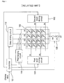
- FIG. 1 is a block diagram illustrating a common light emitting device.
- the light emitting device includes a panel 100, a controller 102, a first scan driving circuit 106, a discharging circuit 108, a precharging circuit 110, and a data driving circuit 112.
- the panel 100 includes a plurality of pixels E11 to E44 formed in cross areas of data lines D1 to D4 and scan lines S1 to S4.
- the controller 302 receives display data from an outside apparatus, and controls the scan driving circuits 104 and 106, the discharging circuit 108, the precharging circuit 110, and the data driving circuit 112, by using the received display data.
- the first scan driving circuit 104 transmits first scan signals to a part of the scan lines S1 to S4, e.g. S1 and S3.
- the second scan driving circuit 106 transmits second scan signals to the other scan lines S2 and S4. As a result, the scan lines S1 to S4 are connected in sequence to a ground.
- the discharging circuit 108 is connected to the data lines D1 to D4, and discharges the data lines to a certain discharge voltage. For example, the discharging circuit 108 discharges the data lines D1 to D4 to a zener voltage of a zener diode ZD by using the zener diode included therein.
- the precharging circuit 110 provides a precharge current corresponding to the display data to the discharged data lines D1 to D4 under control of the controller 102.
- the data driving circuit 112 provides data signals, i.e. data current, corresponding to the display data to the precharged data lines D1 to D4 under control of the controller 102. As a result, pixels E11 to E44 emit a light.
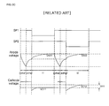
- FIG. 2A and FIG. 2B are views schematically illustrating circuitries of the light emitting device of FIG. 1.
- FIG. 2C and FIG. 2D are timing diagrams illustrating a process of driving the light emitting device.
- cathode voltages VC11 to VC44 will be explained, and then the process of driving the light emitting device will be described in detail.
- cathode voltages VC11 to VC 41 of the pixels E11 to E41 corresponding to a first scan line S1 will be described as an example of the cathode voltages VC11 to VC44 for convenience of the description.
- a resistor between a pixel E11 and the ground is scan resistor Rs
- a resistor between a pixel E21 and the ground is Rs+Rp
- a resistor between a pixel E31 and the ground is Rs+2Rp
- a resistor between a pixel E41 and the ground is Rs+3Rp.
- the cathode voltages VC11 to VC41 of the pixels E11 to E41 are proportioned to corresponding resistors, and thus the cathode voltages VC41, VC31, VC21 and VC11 have sequential magnitude.
- a resistor between a pixel E12 and the ground is Rs+3Rp, and so a cathode voltage VC12 is higher than the cathode voltage VC11.
- a switch SW is turned on, and so the data lines D1 to D4 are discharged to a certain discharge voltage during a first discharge period of time (dcha1).
- the scan lines S1 to S4 are coupled to a non-luminescent source having same magnitude as a driving voltage of the light emitting device.
- a precharge current corresponding to first display data is provided to the data lines D1 to D4.
- the first scan line S1 is coupled to the ground as shown in FIG. 2A, and the other scan lines S2 to S4 are coupled to the non-luminescent source.
- the pixel E41 is preset to have same brightness as the pixel E11.
- the data lines D1 and D4 are discharged to the same discharge voltage, and so anode voltages VA11 and VA41 of pixels E11 and E41 have same magnitude according to the data currents I11 and I41, as shown in FIG. 2D.
- the pixel E11 emits a light having a brightness corresponding to the difference of the anode voltage VA11 and the cathode voltage VC11
- the pixel E41 emits a light having a brightness corresponding to the difference of the anode voltage VA41 and the cathode voltage VC41.
- the anode voltages VA11 and VA41 have same magnitude, but the cathode voltage VC41 is higher than the cathode voltage VC11. Accordingly, though the pixels E11 and E41 are preset to emit a light having the same brightness, the pixel E41 has brightness smaiier than the pixel E11. This is referred to as cross-talk phenomenon.
- the scan lines S1 to S4 are coupled to the non-luminescent source, and the switch SW is turned on. As a result, the data lines D1 to D4 are discharged up to a certain discharge voltage during a second discharge period of time (dcha2).
- a precharge current corresponding to second display data is provided to the data lines D1 to D4, wherein the second display data are inputted to the controller 102 after the first display data are inputted to the controller 102.
- the second scan line S2 is coupled to the ground, and the other scan lines S1, S3 and S4 are coupled to the non-luminescent source.
- data currents I12, I22, I32 and I42 corresponding to the second display data are provided to the data lines D1 to D4, and so the pixels E12 to E42 emit a light during a second luminescent period of time (t2).
- the pixel E12 is assumed to be designed to have the same brightness as the pixel E11.
- a discharge voltage corresponding to the second discharge period of time (dcha2) is substantially identical to the discharge voltage corresponding to the first discharge period of time (dcha1), and thus an anode voltage VA12 has same magnitude as the anode voltage VA11.
- the pixel E11 emits a light having a brightness corresponding to the difference of the anode voltage VA11 and the cathode voltage VC11
- the other pixel E12 emits a light having a brightness corresponding to the difference of the anode voltage VA12 and the cathode voltage VC12.
- the anode voltage VA11 and VA12 have same magnitude, but the cathode voltage VC12 is higher than the cathode voltage VC11. Accordingly, though the pixels E11 and E12 are preset to have the same brightness, the pixel E12 has brightness smaller than the other pixel E11
- a light emitting device includes data lines, scan lines, a plurality of pixels, and a discharging circuit.
- the data lines are disposed in a first direction.
- the scan lines are disposed in a second direction different from the first direction.
- the pixels are formed in cross areas of the data lines and the scan lines.
- the discharging circuit discharges at least two data lines.
- the two data lines are discharged to different discharge voltages.
- a light emitting device includes data lines, scan lines, and a plurality of pixels.
- the data lines are disposed in a first direction.
- the scan lines are disposed in a second direction different from the first direction.
- the pixels are formed in cross areas of the data lines and the scan lines.
- an anode voltage of at least one pixel has magnitude corresponding to its cathode voltage and display data.
- an electroluminescent device includes data lines, scan lines, a plurality of pixels, a first sub discharging circuit, and a second sub discharging circuit.
- the data lines are disposed in a first direction.
- the scan lines are disposed in a second direction different from the first direction.
- the pixels are formed in cross areas of the data lines and the scan lines.
- the first sub discharging circuit provides a first voltage to a first outmost data line of the data lines.
- the second sub discharging circuit provides a second voltage to a second outmost data line.
- the second voltage has different magnitude from the first voltage.
- a method of driving a light emitting device having a plurality of pixels formed in cross areas of data lines and scan lines includes providing a first voltage to a first outmost data line of the data lines; and providing a second voltage to a second outmost data line.
- each anode voltage of pixels corresponding to the scan line has different size depending on corresponding cathode voltage.
- the discharge voltages are changed depending on the cathode voltages, and thus cross-talk phenomenon is not occurred.
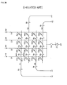
- FIG. 3 is a block diagram illustrating a light emitting device according to a first embodiment of the present invention.
- the light emitting device of the present invention includes a panel 300, a controller 302, a first scan driving circuit 304, a second scan driving circuit 306, a discharging circuit 308, a precharging circuit 310, and a data driving circuit 312.
- the light emitting device includes an organic electroluminescent device, a plasma display panel, a liquid crystal display, and others.
- the organic electroluminescent device will be described as an example of the light emitting device for convenience of the description.
- the panel 300 includes a plurality of pixels E11 to E44 formed in cross areas of data lines D1 to D4 and scan lines S1 to S4.
- Each of the pixels E11 to E44 includes an anode electrode layer, an organic layer, and a cathode electrode layer formed in sequence on a substrate.
- the controller 302 receives display data, e.g. RGB data, inputted from an outside apparatus, and controls the scan driving circuits 304 and 306, the discharging circuit 308, the precharging circuit 310, and the data driving circuit 312, by using the received display data.
- the controller 302 may store the received display data in its memory.
- the first scan driving circuit 304 transmits first scan signals to a part of the scan lines S1 to S4, e.g. S1 and S3.
- the second scan driving circuit 306 transmits second scan signals to the other scan lines S2 and S4.
- the scan lines S1 to S4 are coupled to a luminescent source, e.g. ground.
- the discharging circuit 308 makes the data lines D1 to D4 discharge voltages corresponding to cathode voltages of the pixels E11 to E44, and includes a first sub discharging circuit 320 and a second sub discharging circuit 322.
- the first sub discharging circuit 320 is coupled to a first outmost data line D1 of outmost data lines D1 and D4 as shown in FIG. 3, and provides a first voltage to the first outmost data line D1.
- the second sub discharging circuit 322 is coupled to a second outmost data line D4 as shown in FIG. 3, and provides a second voltage to the second outmost data line D4.
- the second voltage has a different magnitude from the first voltage.
- the precharging circuit 310 provides a precharge current corresponding to the display data to the discharged data lines D1 to D4 under control of the controller 302.
- the data driving circuit 312 provides data signals, i.e. data current, corresponding to the display data to the precharged data lines D1 to D4 under control of the controller 302. As a result, the pixels E11 to E44 emit a light.
- the first scan line S1 is coupled to the ground, and the other scan lines S2 to S4 are coupled to a non-luminescent source having the same voltage as the driving voltage of the light emitting device.
- a first data current corresponding to first display data is provided to the data lines D1 to D4.
- the first data current provided to the data lines D1 to D4 passes to the ground through corresponding pixels E11 to E41 and the first scan line S1.
- the pixels E11 to E41 corresponding to the first scan line S1 emit a light.
- the data lines D1 to D4 are discharged up to voltages corresponding to cathode voltages of the pixels E11 to E41 for a discharge period of time.
- the data lines D1 to D4 are precharged to a level corresponding to second display data inputted to the controller 302 after the first display data are inputted to the controller 302.
- the second scan line S2 is coupled to the ground, and the other scan lines S1, S3 and S4 are coupled to the non-luminescent source.
- a second data current corresponding to the second display data is provided to the data lines D1 to D4.
- the pixels E12 to E42 corresponding to the second scan line S2 emit a light.
- the data lines D1 to D4 are discharged for a discharge period of time.
- the above process is repeatedly performed from the first scan line S1 to the fourth scan line S4.
- FIG. 4A and FIG. 4B are views schematically illustrating circuitries of the light emitting device of FIG. 3.
- FIG. 4C and FIG. 4D are timing diagrams illustrating a process of driving the light emitting device.
- the first sub discharging circuit 320 includes a first switch (SW1) 400, a first digital-analog converter (hereinafter, referred to as "first DAC”) 402, and a first buffer 404.
- SW1 first switch
- first DAC first digital-analog converter
- the second sub discharging circuit 322 includes a second switch (SW2) 406, a second DAC 408, and a second buffer 410.
- cathode voltages VC11 to VC44 will be explained, and then the process of driving the light emitting device will be described in detail.
- cathode voltages VC11 to VC 41 corresponding to a first scan line S1 will be described as an example of the cathode voltages VC11 to VC44 for convenience of the description.
- a resistor between a pixel E11 and the ground is scan resistor Rs
- a resistor between a pixel E21 and the ground is Rs+Rp
- a resistor between a pixel E31 and the ground is Rs+2Rp
- a resistor between a pixel E41 and the ground is Rs+3Rp.
- the cathode voltages VC11 to VC41 of the pixels E11 to E41 are proportioned to resistors between corresponding pixel and the ground, and thus the values are high in the order of the cathode voltages VC41, VC31, VC21 and VC11.
- a resistor between a pixel E12 and the ground is Rs+3Rp, and so the cathode voltage VC12 is higher than the cathode voltage VC11.
- the discharging circuit 308 discharges the data lines D1 to D4.
- the first switch SW1 and the second switch SW2 are turned on, and the scan lines S1 to S4 are coupled to the non-luminescent source having a voltage V2.
- the first DAC 402 outputs a first level voltage in accordance with a first outside voltage V3 inputted from the outside.
- the outputted first level voltage is inputted to the first buffer 404.
- the second DAC 408 outputs a second level voltage in accordance with a second outside voltage V4 inputted from the outside.
- the outputted second level voltage is inputted to the second buffer 410.
- the first buffer 404 provides a certain current to the first outmost data line D1 in accordance with the inputted first level voltage, and so the first outmost data line D1 has a first voltage.
- the second buffer 410 provides a certain current to the second outmost data line D4 in accordance with the inputted second level voltage, and so the second outmost data line D4 has a second voltage different from the first voltage. Accordingly, the data lines D1 to D4 have sequentially different magnitudes of voltages, and thus are discharged up to different disaharge levels from each other at the time of discharge.
- the cathode voltage VC41 is higher than the cathode voltage VC11, and thus the second voltage is higher than the first voltage.
- the pixel E41 is assumed to be designed to have the same brightness as the pixel E11.
- the cathode voltage VC41 is higher than the cathode voltage VC11, and thus the fourth data line D4 is discharged up to a discharge voltage higher than the first data line D1 during a first discharge period of time (dcha1) as shown in FIG. 4D.
- the data lines D1 to D4 are precharged for a first precharge period of time (pcha1).
- the fourth data line D4 is discharged up to the discharge voltage higher than the first data line D1
- the fourth data line D4 is precharged to a voltage higher than the first data line D1.
- the first scan line S1 is coupled to the ground, and the other scan lines S2 to S4 are coupled to the non-luminescent source.
- data currents I11 to I41 corresponding to first display data are provided to the data lines D1 to D4, and then the data currents I11 to I41 provided to the data lines D1 to D4 passes to the ground through corresponding pixels E11 to E41 and the first scan line S1.
- the pixels E11 to E41 corresponding to the first scan line S1 emit a light for a first light emitting time t1. Only, each pixel emits a light whose brightness corresponds to the difference of its anode voltage and cathode voltage.
- the fourth data line D4 is more precharged than the first data line D1, and thus the anode voltage VA41 is higher than the anode voltage VA11. Accordingly, the brightness of the pixel E41, i.e. VA41-VC41, is substantially identical to the brightness of the pixel E11, i.e. VA11-VC11.
- a process of driving the pixel E21 and the pixel E31 is substantially identical to the process of the pixel E11 and the pixel E41. Accordingly, since the pixels E11 to E41 are designed to emit a light having the same brightness, the pixels E11 to E41 have substantially the same brightness.
- the scan lines S1 to S4 are coupled to the non-luminescent source, and the first and second switches SW1 and SW2 are turned on.
- the first sub discharging circuit 320 provides a third voltage to the first outmost data line D1
- the second sub discharging circuit 322 provides a fourth voltage to the second outmost data line D4.
- a cathode voltage VC12 is higher than a cathode voltage VC42
- the third voltage is higher than the fourth voltage. Accordingly, the data lines D1 to D4 are discharged up to discharge voltages having sequential magnitude.
- the data line D1 is discharged up to a higher discharge voltage for a second discharge period of time (dcha2) than a first discharge period of time (dcha1).
- a precharge current corresponding to second display data is provided to the data lines D1 to D4.
- the second display data are inputted to the controller 302 after the first display data are inputted to the controller 302.
- the second scan line S2 is coupled to the ground, and the other scan lines S1, S3 and S4 are coupled to the non-luminescent source.
- the anode voltage of a pixel is changed depending on the cathode voltage of the pixel, unlike in the light emitting device in the art. Accordingly, when the pixels are preset to have the same brightness, the pixels emit light having the same brightness irrespective of their cathode voltages. Hence, the cross-talk phenomenon is not occurred in the panel 300 included in the light emitting device of the present invention.
- FIG. 5 is a view illustrating a circuitry of a light emitting device according to a second embodiment of the present invention.
- the light emitting device of the second embodiment further includes one or more third sub discharging circuits 500 than the light emitting device of the first embodiment.
- the third sub discharging circuit 500 provides a certain voltage to data line located between the outmost data lines D1 and D4.
- the voltage has a magnitude of voltages provided to the outmost data lines D1 and D4.
- the cathode voltages corresponding to a scan line are linearly changed. Accordingly, the cathode voltages could be compensated by using only the two sub discharging circuits 320 and 322.
- the light emitting device compensates the nonlinearly changing cathode voltages by using the third sub discharging circuit 500.
- the third sub discharging circuit 500 of the present invention includes a third switch 502, a third DAC 504, and a third buffer 506. Since the elements of the third sub discharging circuit 500 are the same as in the first embodiment, any further detailed descriptions concerning the same elements will be omitted.
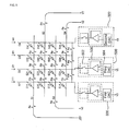
- FIG. 6 is a block diagram illustrating a light emitting device according to a third embodiment of the present invention.
- FIG. 7 is a view illustrating a circuitry of the light emitting device of FIG. 6.
- the light emitting device of the present invention includes a panel 600, a controller 602, a first scan driving circuit 604, a second scan driving circuit 606, a discharging circuit 608, a precharging circuit 610, and a data driving circuit 612.
- the discharging circuit 608 includes a first sub discharging circuit 620, a second sub discharging circuit 622, and a third sub discharging circuit 624.
- the first sub discharging circuit 620 discharges the data lines D1 to D4 up to a certain discharge voltage. For example, the first sub discharging circuit 620 discharges the data lines D1 to D4 up to a zener voltage of a zener diode 702 by using the zener diode 702 included therein, as shown in FIG. 7.
- the second and third discharging circuits 622 and 624 compensate the cathode voltages of the pixels E11 to E44.
- the second and third sub discharging circuits 622 and 624 include switches 704 and 710, DACs 706 and 712, and buffers 708 and 714.
- the cathode voltages VC11 to VC44 are compensated by using the current outputted from the buffers 404 and 410, and so the power consumption of the light emitting device is high.
- the cathode voltages VC11 to VC44 are compensated by using the buffers 708 and 714 after the data lines D1 to D4 are discharged up to a certain discharge voltage by using the zener diode 702. Accordingly, the power consumption of the light emitting device in the third embodiment is lower than that of the light emitting device in the first embodiment.
- FIG. 8 is a block diagram illustrating a light emitting device according to a fourth embodiment of the present invention.
- the light emitting device of the present invention includes a panel 800, a controller 802, a scan driving circuit 804, a discharging circuit 806, a precharging circuit 808, and a data driving circuit 810. Since the elements of the present embodiment are the same as the first embodiment, any further detailed description concerning the same elements will be omitted.
- the scan driving circuit 804 is disposed in one direction of the panel 800 unlike the other embodiments.
Landscapes
- Engineering & Computer Science (AREA)
- Physics & Mathematics (AREA)
- Computer Hardware Design (AREA)
- General Physics & Mathematics (AREA)
- Theoretical Computer Science (AREA)
- Control Of Indicators Other Than Cathode Ray Tubes (AREA)
- Electroluminescent Light Sources (AREA)
- Control Of El Displays (AREA)
Applications Claiming Priority (1)
| Application Number | Priority Date | Filing Date | Title |
|---|---|---|---|
| KR20050115630 | 2005-11-30 |
Publications (2)
| Publication Number | Publication Date |
|---|---|
| EP1793365A2 true EP1793365A2 (de) | 2007-06-06 |
| EP1793365A3 EP1793365A3 (de) | 2008-05-07 |
Family
ID=37781755
Family Applications (1)
| Application Number | Title | Priority Date | Filing Date |
|---|---|---|---|
| EP06006141A Withdrawn EP1793365A3 (de) | 2005-11-30 | 2006-03-24 | Lichtemittierende Vorrichtung und Ansteuerverfahren dafür |
Country Status (5)
| Country | Link |
|---|---|
| US (1) | US20070120777A1 (de) |
| EP (1) | EP1793365A3 (de) |
| JP (1) | JP2007156389A (de) |
| KR (1) | KR100752341B1 (de) |
| CN (1) | CN100574545C (de) |
Cited By (1)
| Publication number | Priority date | Publication date | Assignee | Title |
|---|---|---|---|---|
| EP1850314A2 (de) | 2006-04-28 | 2007-10-31 | LG Electronics Inc. | Lichtemittierende Vorrichtung und Ansteuerverfahren dafür |
Families Citing this family (9)
| Publication number | Priority date | Publication date | Assignee | Title |
|---|---|---|---|---|
| KR100756275B1 (ko) * | 2006-04-28 | 2007-09-06 | 엘지전자 주식회사 | 발광 소자 및 이를 구동하는 방법 |
| JP2010243736A (ja) * | 2009-04-03 | 2010-10-28 | Sony Corp | 表示装置 |
| US9105241B2 (en) * | 2009-05-09 | 2015-08-11 | Chen-Jean Chou | Structure of light emitting device array and drive method for display light source |
| CN103943066B (zh) * | 2014-03-27 | 2016-02-03 | 京东方科技集团股份有限公司 | 一种像素电路及其驱动方法、显示装置 |
| KR102333142B1 (ko) * | 2014-04-04 | 2021-12-02 | 삼성디스플레이 주식회사 | 화소 및 상기 화소를 포함하는 유기발광 표시장치 |
| KR102738329B1 (ko) * | 2020-10-30 | 2024-12-04 | 엘지디스플레이 주식회사 | 표시패널과 이를 이용한 표시장치 |
| CN117524083A (zh) * | 2022-08-05 | 2024-02-06 | 联咏科技股份有限公司 | 发光二极管面板及其驱动装置 |
| TWI858653B (zh) * | 2023-04-12 | 2024-10-11 | 凌巨科技股份有限公司 | 顯示裝置及其放電方法 |
| TWI898670B (zh) | 2024-01-24 | 2025-09-21 | 聯詠科技股份有限公司 | 顯示面板的預充電控制方法及裝置、顯示系統及其驅動方法 |
Citations (2)
| Publication number | Priority date | Publication date | Assignee | Title |
|---|---|---|---|---|
| EP1091340A2 (de) | 1999-10-05 | 2001-04-11 | Nec Corporation | Verfahren und Einrichtung zur Steuerung eines organischen Dünnschicht-Elektrolumineszenzanzeigegerät |
| EP1553551A2 (de) | 2004-01-10 | 2005-07-13 | Lg Electronics Inc. | Gerät und Verfahren zum Steuern einer flachen Anzeigetafel |
Family Cites Families (13)
| Publication number | Priority date | Publication date | Assignee | Title |
|---|---|---|---|---|
| JPH11161219A (ja) * | 1997-09-10 | 1999-06-18 | Toray Ind Inc | 発光装置駆動回路 |
| JP3403097B2 (ja) * | 1998-11-24 | 2003-05-06 | 株式会社東芝 | D/a変換回路および液晶表示装置 |
| JP2002108284A (ja) * | 2000-09-28 | 2002-04-10 | Nec Corp | 有機el表示装置及びその駆動方法 |
| JP3951687B2 (ja) * | 2001-08-02 | 2007-08-01 | セイコーエプソン株式会社 | 単位回路の制御に使用されるデータ線の駆動 |
| KR100438659B1 (ko) * | 2002-02-18 | 2004-07-02 | 주식회사 실리콘웍스 | 엘씨디 선구동을 위한 칼럼 구동 집적 회로 및 칼럼 구동방법 |
| KR100609748B1 (ko) * | 2002-05-09 | 2006-08-09 | 엘지전자 주식회사 | 일렉트로-루미네센스 표시패널 구동장치 |
| JP2004233651A (ja) * | 2003-01-30 | 2004-08-19 | Samsung Oled Co Ltd | 電界発光ディスプレイパネルの駆動方法 |
| JP2005003836A (ja) * | 2003-06-11 | 2005-01-06 | Tohoku Pioneer Corp | 発光表示パネルの駆動装置および駆動方法 |
| KR100515351B1 (ko) * | 2003-07-08 | 2005-09-15 | 삼성에스디아이 주식회사 | 표시 패널, 이를 이용한 발광 표시 장치 및 그 구동 방법 |
| US7400098B2 (en) * | 2003-12-30 | 2008-07-15 | Solomon Systech Limited | Method and apparatus for applying adaptive precharge to an electroluminescence display |
| JP4640755B2 (ja) * | 2004-01-19 | 2011-03-02 | 東北パイオニア株式会社 | 発光表示パネルの駆動装置および駆動方法 |
| KR101085911B1 (ko) * | 2004-07-30 | 2011-11-23 | 매그나칩 반도체 유한회사 | 유기전계 발광장치 |
| JP2006047510A (ja) * | 2004-08-02 | 2006-02-16 | Oki Electric Ind Co Ltd | 表示パネル駆動回路と駆動方法 |
-
2006
- 2006-03-17 US US11/377,274 patent/US20070120777A1/en not_active Abandoned
- 2006-03-24 EP EP06006141A patent/EP1793365A3/de not_active Withdrawn
- 2006-03-29 JP JP2006091397A patent/JP2007156389A/ja not_active Withdrawn
- 2006-03-31 CN CNB2006100738533A patent/CN100574545C/zh not_active Expired - Fee Related
- 2006-05-15 KR KR1020060043582A patent/KR100752341B1/ko active Active
Patent Citations (2)
| Publication number | Priority date | Publication date | Assignee | Title |
|---|---|---|---|---|
| EP1091340A2 (de) | 1999-10-05 | 2001-04-11 | Nec Corporation | Verfahren und Einrichtung zur Steuerung eines organischen Dünnschicht-Elektrolumineszenzanzeigegerät |
| EP1553551A2 (de) | 2004-01-10 | 2005-07-13 | Lg Electronics Inc. | Gerät und Verfahren zum Steuern einer flachen Anzeigetafel |
Cited By (4)
| Publication number | Priority date | Publication date | Assignee | Title |
|---|---|---|---|---|
| EP1850314A2 (de) | 2006-04-28 | 2007-10-31 | LG Electronics Inc. | Lichtemittierende Vorrichtung und Ansteuerverfahren dafür |
| EP1850314A3 (de) * | 2006-04-28 | 2009-12-16 | LG Display Co., Ltd. | Lichtemittierende Vorrichtung und Ansteuerverfahren dafür |
| US7898508B2 (en) | 2006-04-28 | 2011-03-01 | Lg Display Co., Ltd. | Light emitting device and method of driving the same |
| US8416160B2 (en) | 2006-04-28 | 2013-04-09 | Lg Display Co., Ltd. | Light emitting device and method of driving the same |
Also Published As
| Publication number | Publication date |
|---|---|
| KR100752341B1 (ko) | 2007-08-27 |
| EP1793365A3 (de) | 2008-05-07 |
| JP2007156389A (ja) | 2007-06-21 |
| US20070120777A1 (en) | 2007-05-31 |
| CN100574545C (zh) | 2009-12-23 |
| KR20070056905A (ko) | 2007-06-04 |
| CN1976553A (zh) | 2007-06-06 |
Similar Documents
| Publication | Publication Date | Title |
|---|---|---|
| US8274455B2 (en) | Pixel driving circuit for a display device and a driving method thereof | |
| CN100578588C (zh) | 有机电致发光显示装置及其驱动方法 | |
| JP2000235370A (ja) | 有機エレクトロルミネッセンス素子駆動装置 | |
| EP1793365A2 (de) | Lichtemittierende Vorrichtung und Ansteuerverfahren dafür | |
| EP1763012A2 (de) | Lichtemittierende Vorrichtung und Ansteuerverfahren dafür | |
| KR20070042071A (ko) | 표시 패널의 구동방법 및 그 구동장치 | |
| US8416160B2 (en) | Light emitting device and method of driving the same | |
| US8094094B2 (en) | Light emitting device having a discharging circuit and method of driving the same | |
| US20070139318A1 (en) | Light emitting device and method of driving the same | |
| US7365716B2 (en) | Light emitting device and method of driving the same | |
| CN100555376C (zh) | 光发射设备和驱动该设备的方法 | |
| KR100784754B1 (ko) | 발광 소자 및 이를 구동하는 방법 | |
| KR100624134B1 (ko) | 유기전계발광표시장치의 구동방법 | |
| KR100752342B1 (ko) | 발광 소자 및 이를 구동하는 방법 | |
| KR100653478B1 (ko) | 유기 전계발광 표시장치 | |
| KR100752340B1 (ko) | 발광 소자 및 이를 구동하는 방법 | |
| KR100819137B1 (ko) | 발광 소자 및 이를 구동하는 방법 | |
| KR20080003995A (ko) | 발광 소자 및 이를 구동하는 방법 |
Legal Events
| Date | Code | Title | Description |
|---|---|---|---|
| PUAI | Public reference made under article 153(3) epc to a published international application that has entered the european phase |
Free format text: ORIGINAL CODE: 0009012 |
|
| 17P | Request for examination filed |
Effective date: 20060324 |
|
| AK | Designated contracting states |
Kind code of ref document: A2 Designated state(s): AT BE BG CH CY CZ DE DK EE ES FI FR GB GR HU IE IS IT LI LT LU LV MC NL PL PT RO SE SI SK TR |
|
| AX | Request for extension of the european patent |
Extension state: AL BA HR MK YU |
|
| PUAL | Search report despatched |
Free format text: ORIGINAL CODE: 0009013 |
|
| AK | Designated contracting states |
Kind code of ref document: A3 Designated state(s): AT BE BG CH CY CZ DE DK EE ES FI FR GB GR HU IE IS IT LI LT LU LV MC NL PL PT RO SE SI SK TR |
|
| AX | Request for extension of the european patent |
Extension state: AL BA HR MK YU |
|
| 17Q | First examination report despatched |
Effective date: 20080626 |
|
| AKX | Designation fees paid |
Designated state(s): AT BE BG CH CY CZ DE DK EE ES FI FR GB GR HU IE IS IT LI LT LU LV MC NL PL PT RO SE SI SK TR |
|
| RAP1 | Party data changed (applicant data changed or rights of an application transferred) |
Owner name: LG ELECTRONICS INC. |
|
| GRAP | Despatch of communication of intention to grant a patent |
Free format text: ORIGINAL CODE: EPIDOSNIGR1 |
|
| INTG | Intention to grant announced |
Effective date: 20130617 |
|
| RIN1 | Information on inventor provided before grant (corrected) |
Inventor name: KIM. JI HUN |
|
| STAA | Information on the status of an ep patent application or granted ep patent |
Free format text: STATUS: THE APPLICATION IS DEEMED TO BE WITHDRAWN |
|
| 18D | Application deemed to be withdrawn |
Effective date: 20131001 |