EP1792353B1 - High output small area group iii nitride leds - Google Patents
High output small area group iii nitride leds Download PDFInfo
- Publication number
- EP1792353B1 EP1792353B1 EP05812300.1A EP05812300A EP1792353B1 EP 1792353 B1 EP1792353 B1 EP 1792353B1 EP 05812300 A EP05812300 A EP 05812300A EP 1792353 B1 EP1792353 B1 EP 1792353B1
- Authority
- EP
- European Patent Office
- Prior art keywords
- light emitting
- layer
- emitting diode
- diode
- substrate
- Prior art date
- Legal status (The legal status is an assumption and is not a legal conclusion. Google has not performed a legal analysis and makes no representation as to the accuracy of the status listed.)
- Expired - Lifetime
Links
Images
Classifications
-
- H—ELECTRICITY
- H10—SEMICONDUCTOR DEVICES; ELECTRIC SOLID-STATE DEVICES NOT OTHERWISE PROVIDED FOR
- H10H—INORGANIC LIGHT-EMITTING SEMICONDUCTOR DEVICES HAVING POTENTIAL BARRIERS
- H10H20/00—Individual inorganic light-emitting semiconductor devices having potential barriers, e.g. light-emitting diodes [LED]
- H10H20/80—Constructional details
- H10H20/83—Electrodes
- H10H20/832—Electrodes characterised by their material
- H10H20/835—Reflective materials
-
- H—ELECTRICITY
- H10—SEMICONDUCTOR DEVICES; ELECTRIC SOLID-STATE DEVICES NOT OTHERWISE PROVIDED FOR
- H10H—INORGANIC LIGHT-EMITTING SEMICONDUCTOR DEVICES HAVING POTENTIAL BARRIERS
- H10H20/00—Individual inorganic light-emitting semiconductor devices having potential barriers, e.g. light-emitting diodes [LED]
- H10H20/80—Constructional details
- H10H20/81—Bodies
- H10H20/819—Bodies characterised by their shape, e.g. curved or truncated substrates
-
- H—ELECTRICITY
- H01—ELECTRIC ELEMENTS
- H01L—SEMICONDUCTOR DEVICES NOT COVERED BY CLASS H10
- H01L2224/00—Indexing scheme for arrangements for connecting or disconnecting semiconductor or solid-state bodies and methods related thereto as covered by H01L24/00
- H01L2224/01—Means for bonding being attached to, or being formed on, the surface to be connected, e.g. chip-to-package, die-attach, "first-level" interconnects; Manufacturing methods related thereto
- H01L2224/42—Wire connectors; Manufacturing methods related thereto
- H01L2224/47—Structure, shape, material or disposition of the wire connectors after the connecting process
- H01L2224/48—Structure, shape, material or disposition of the wire connectors after the connecting process of an individual wire connector
- H01L2224/481—Disposition
- H01L2224/48151—Connecting between a semiconductor or solid-state body and an item not being a semiconductor or solid-state body, e.g. chip-to-substrate, chip-to-passive
- H01L2224/48221—Connecting between a semiconductor or solid-state body and an item not being a semiconductor or solid-state body, e.g. chip-to-substrate, chip-to-passive the body and the item being stacked
- H01L2224/48245—Connecting between a semiconductor or solid-state body and an item not being a semiconductor or solid-state body, e.g. chip-to-substrate, chip-to-passive the body and the item being stacked the item being metallic
- H01L2224/48247—Connecting between a semiconductor or solid-state body and an item not being a semiconductor or solid-state body, e.g. chip-to-substrate, chip-to-passive the body and the item being stacked the item being metallic connecting the wire to a bond pad of the item
-
- H—ELECTRICITY
- H01—ELECTRIC ELEMENTS
- H01L—SEMICONDUCTOR DEVICES NOT COVERED BY CLASS H10
- H01L2924/00—Indexing scheme for arrangements or methods for connecting or disconnecting semiconductor or solid-state bodies as covered by H01L24/00
- H01L2924/15—Details of package parts other than the semiconductor or other solid state devices to be connected
- H01L2924/181—Encapsulation
-
- H—ELECTRICITY
- H10—SEMICONDUCTOR DEVICES; ELECTRIC SOLID-STATE DEVICES NOT OTHERWISE PROVIDED FOR
- H10H—INORGANIC LIGHT-EMITTING SEMICONDUCTOR DEVICES HAVING POTENTIAL BARRIERS
- H10H20/00—Individual inorganic light-emitting semiconductor devices having potential barriers, e.g. light-emitting diodes [LED]
- H10H20/80—Constructional details
- H10H20/81—Bodies
- H10H20/822—Materials of the light-emitting regions
- H10H20/824—Materials of the light-emitting regions comprising only Group III-V materials, e.g. GaP
- H10H20/825—Materials of the light-emitting regions comprising only Group III-V materials, e.g. GaP containing nitrogen, e.g. GaN
Definitions
- the present invention relates to light emitting diodes (LEDs) and in particular relates to LEDs formed with active portions of Group III nitrides on silicon carbide substrates.
- Incandescent lighting is produced by heating a metal filament, usually by passing electric current through a metal filament. The heated filament emits light. Household and other indoor lighting is a common application of incandescent lighting. "Halogen" lighting works on the same general principle, but more efficiently. Fluorescent light is generated by exciting a vapor (typically mercury-containing) with an applied potential difference. Photons emitted by the excited vapor then strike phosphors that emit the visible light. Fluorescent light is also common in household, office and a variety of other applications.
- a light emitting diode is a p-n junction semiconductor diode that emits photons when forward biased.
- light emitting diodes produce light based upon the movement of electrons in a semiconductor material. Therefore, LEDs do not require (although they can be used in conjunction with) vapors or phosphors. They share the desirable characteristics of most semiconductor-based devices, including high efficiency (their emissions include little or no heat), high reliability and long life. For example, typical LEDs have a mean time between failures of between about 100,000 and 1,000,000 hours meaning that a conservative half lifetime for an LED is on the order of 50,000 hours.
- an LED's emitted light has a frequency (which in turn relates directly to wavelength and color in accordance with well-understood principles of physics) based upon the energy difference between permitted energy levels in the material, a characteristic referred to as the bandgap.
- the bandgap is a fundamentally property of the semiconductor material and its doping.
- LEDs formed in silicon Si, bandgap of 1.12 electron volts (eV)
- eV electron volts
- LEDs formed in gallium arsenide bandgap 1.42 eV
- silicon-doped aluminum gallium arsenide AlGaAs
- Such materials include diamond (5.47 eV), silicon carbide (2.99 eV) and Group III nitrides such as GaN (3.4 eV).
- wide bandgap LEDs can be combined with red and green LEDs to produce white light, or with phosphors that produce white light when excited by blue or UV light, or both.
- the Group III nitride compositions i.e., Group III of the periodic table
- GaN, AlGaN, InGaN and AlInGaN are particularly useful for blue-emitting LEDs.
- they are "direct” emitters, meaning that when an electron transition occurs across the bandgap, much of the energy is emitted as light.
- indirect emitters such as silicon carbide
- Group III nitrides offer efficiency advantages over indirect transition materials.
- the bandgap of ternary and quaternary Group III materials depends upon the atomic fraction of the included Group III elements.
- the wavelength (color) of the emission can be tailored (within limits) by controlling the atomic fraction of each Group III element in a ternary or quaternary nitride.
- GaP gallium-arsenide or gallium phosphide
- blue and UV-emitting LEDs have lagged behind GaP-based LED's in their commercial appearance.
- silicon carbide is physically very hard, has no melt phase, and requires high temperatures (on the order of about 1500-2000 °C) for epitaxial or sublimation growth.
- the Group III nitrides have relatively large nitrogen vapor pressures at their melting temperatures and thus are likewise difficult or impossible to grow from a melt.
- lighting is typically quantified as to its output.
- One typical unit of measure is the lumen, defined as a unit of luminous flux equal to the light emitted in a unit solid angle by a uniform point source of one candela (cd) intensity.
- the candela is the base unit of luminous intensity in the International System of Units that is equal to the luminous intensity in a given direction of a source which emits monochromatic radiation of frequency 540 x 10 12 hertz and has a radiant intensity in that direction of 1/683 watt per unit solid angle.
- an intensity of 1200-1800 lumens is typical of incandescent bulbs and 1000-6000 lumens (depending upon circumstances) is typical in natural daylight.
- Light emitting diodes are much less intense, for example on the order of about 10-100 lumens.
- One reason is their small size.
- applications for single (or small groups of) LEDs have historically gravitated towards indication (e.g. the register of a hand-held calculator) rather than illumination (a reading lamp).
- indication e.g. the register of a hand-held calculator
- illumination a reading lamp
- the output of LEDs is often measured in units other than lumens. Additionally, an LED's output also depends upon the applied current, which in turn depends upon the potential difference applied across the diode. Thus, the output of an LED is often referred to as its radiant flux (R f ) and is expressed in milliwatts (mW) at a standard 20 milliamp (mA) drive current.
- blue LEDs and their related derivative devices are becoming more frequently included in consumer electronic devices, particularly small displays.
- Common examples include items such as computer screens, personal digital assistants ("PDAs”) and cellular phones.
- PDAs personal digital assistants
- these small devices drive demand for LEDs with reduced size (“footprint”).
- Such LEDs must still operate at low forward voltages (V f ) and high light output.
- V f forward voltages
- reducing the size of the Group III nitride devices has tended to increase their forward voltage and reduce their radiant flux.
- LEDs examples are described in US 6 410 940 B1 , US 6 403 985 B1 and WO 2004/010509 A2 , for instance.
- the present invention concerns a light emitting diode with the features of claim 1.
- the present invention is a light emitting diode having small size, a low forward voltage, and a high light output resulting in high-efficiency and high output on a per unit area basis.
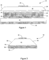
- Figure 1 is a cross sectional view of a light emitting diode broadly designated at 20 according to the present invention.
- the diode 20 includes a transparent silicon carbide substrate 21 which is preferably a single crystal and has a polytype selected from the 3C, 4H, 6H, and 15R polytypes of silicon carbide with 4H often being preferred in the context of the present invention.
- Figure 1 illustrates the diode 20 in the "flip chip" orientation (i.e., mounted for use with the active layers below the substrate), the substrate 21 appears at the top of the diode 20 rather than the bottom. In this orientation, the SiC substrate becomes the primary emitting surface of the LED.
- the diode includes at least one, and preferably several, layers that form the light emitting ("active") portions. Two layers are shown in Figure 1 , an n-type layer 22 and a p-type layer 23. These opposite conductivity type layers provide the opportunity for current to flow through the diode and the resulting combination of electrons and holes that generate the emitted photons. Although only two Group III nitride layers are illustrated in Figure 1 , it will be understood that in other contexts, additional layers can be used including superlattice structures and multiple quantum wells. Such structures are well-understood in this art and can be practiced in the context of the present invention without undue experimentation.
- the embodiment illustrated in Figure 1 also includes a mirror layer 24 which is typically formed of silver (Ag) or a silver-platinum (Ag/Pt) alloy.
- the silver-based layer also provides electrical contact to the active layers 22, 23.
- a barrier layer 25 typically formed of a titanium tungsten (TiW) alloy, or platinum, or both, or of titanium tungsten nitride (TiWN), encloses the silver-based layer 24 in order to prevent undesired migration and reaction of silver with other portions of the device.
- a solder layer 26 is attached to the barrier layer 25 typically, but not exclusively, based upon the method of making the diode. These and other structural features are set forth in the previously cited '042 application.
- a metal or conductive semiconductor layer 27 forms a physical support and a backside ohmic contact 30 completes the structure and, with the top ohmic contact 28, provides the full current path for injecting current through the diode 20.
- the metal or semiconductor support layer 27 can be omitted, with or without the solder layer 26.
- the backside ohmic contact 30 is positioned against the mirror and barrier metals 24, 25.
- the active layers are typically Group III nitrides, with gallium nitride (GaN), indium gallium nitride (InGaN), aluminum gallium nitride (AlGaN), and aluminum indium gallium nitride (AlInGaN) being appropriate selections.
- the Group III nitrides offer the opportunity to change the dominant wavelength by changing the atomic fraction of the Group III element in the ternary and quaternary combinations.
- these formulas can be more exactly expressed as Al x In y Ga 1-x-y N in which x and y can range from 0 to 1, and inclusive of either, with the qualification that x + y must always equal 1 or less.
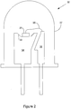
- FIG. 2 is a cross-sectional view of a lamp that incorporates diodes according to the present invention in standard packaging.
- the lamp is broadly designated at 32 and includes elements that are well understood by those of ordinary skill in this art. Indeed, one of the advantages of the diode disclosed therein is that its size and orientation permit it to be mounted in standard packaging with associated benefits to the manufacturer and the end-user.
- the lamp 32 includes the diode which is again indicated at 20.
- the diode rests in a reflective cup 33 which in the type of diode illustrated in Figure 2 is sometimes referred to as the anvil 34 and also forms one of the electrical contacts to the lamp 32.
- the anvil is conductive and typically formed of metal. Although for clarity's sake Figure 2 shows the diode 20 as resting in the die cup 33, in actual practice it is typically fixed in place with a conductive glue or solder (not shown).
- the anvil 34 makes electrical contact with the backside ohmic contact 30 ( Figure 1 ) of the diode 20 and a top bond wire 35 makes electrical contact to the top ohmic contact 28 (also in Figure 1 ) of the diode 20.
- the anvil 34 makes direct contact with the solder layer 26 or the barrier metal layer 25.
- the top bond wire 35 connects to another larger electrode 36 referred to as the post.
- the entire package includes the polymer housing or lens 37 the size and shape of which, along with the material, are chosen for specific output purposes.
- the active layers 22, 23 are adjacent the floor of the die cup 33 with the silicon carbide substrate 21 facing upwardly away from the cup.
- Figure 2 is an exemplary and to some extent schematic diagram and very similar packages can include a surface mount, a metal can, or a metal header, as well as the epoxy lens illustrated in Figure 2 .
- the invention is not limited to use in a 5 mm package, the 5 mm package (also known as the T-1 3 ⁇ 4 type) is commonly understood, widely available and frequently used in the industry. It thus provides an appropriate expression of the invention in terms of its packaging and use.
- the LED of the present invention has an advantageous output on a per unit area basis that comprises an area of less than 100,000 ⁇ 2 , forward voltage of less than 4.0 volts, a radiant flux of at least 24 milliwatts at 20 milliamp drive current, and a dominant wavelength between about 395 and 540 nm.
- the forward voltage (V f ) is defined as the voltage at a given current.
- V f the forward voltage
- diodes according to the invention can operate at a forward voltage of 4.0 volts or less at 20 milliamps drive current.
- Radiant flux is measured by placing an encapsulated lamp of the T1-3 ⁇ 4 type in an integrating sphere attached to a spectrometer, with the Labsphere Omni LTS spectrometer for visible LEDs being an exemplary measurement device. Radiant flux is measured in units of power (Watts).
- the term "dominant wavelength" describes a measure of the hue sensation produced in the human eye by a light emitting diode.
- the dominant wavelength is determined by drawing a straight line through the color coordinates of a reference illuminant and the measured chromaticity coordinates of the LED in the International Commission on Illumination (CIE) 1931 chromaticity diagram. The intersection of the straight-line on the boundary of the chromaticity diagram gives the dominant wavelength.
- CIE International Commission on Illumination
- the peak wavelength is the wavelength at the maximum spectral power.
- the peak wavelength may have less significance for practical purposes because two different light emitting diodes may have the same peak wavelength, but different color perception.
- the lens 37 is used to change the direction and distribution of the light rays (i.e., the spatial distribution pattern) and for some light emitting diodes is colored to serve as an optical filter. Because diodes according to the present invention are frequently used in conjunction with the production of white light, colored lenses are less commonly used.
- the radiant flux of a light emitting diode is typically measured using an integrating sphere, of which the device referenced above is entirely appropriate, but not limiting.
- Radiant flux which is also referred to as the radiant power, is the rate (d ⁇ /dt) at which the radiation field transfers radiant energy from one region to another.
- the rate (d ⁇ /dt) at which the radiation field transfers radiant energy from one region to another is the rate (d ⁇ /dt) at which the radiation field transfers radiant energy from one region to another.
- theta ( ⁇ ) is the radiant energy
- the unit of radiant power is the watt.
- Diodes according to the present invention typically have a dominant wavelength between about 395 and 540 nm, placing them in the green, blue, violet and ultraviolet portions of the electromagnetic spectrum.
- diodes according to the invention have dominant wavelengths of between about 450 and 480 nm with preferred output wavelengths being between about 455 and 465 nm. This places their output squarely in the blue portion of visible spectrum which offers a number of advantages for full-color and white light for displays and related purposes.
- Diodes according to the invention can have a radiant flux of at least 24 milliwatts at the 20 milliamp drive current which is a typical standard in measuring the performance of light emitting diodes of all types, and thus provides a useful comparison for diodes according to the present invention.
- Blue light emitting diodes according to the present invention can be incorporated into pixels, particularly in combination with those that form other primary colors (red and green) to provide the opportunity for full-color displays.
- the term "external quantum efficiency" is used to describe the ratio of emitted light intensity to current flow (e.g., photons out/electrons in). Photons can be lost through absorption within the semiconductor material itself, through reflection losses when light passes from the semiconductor to air because of the differences in refractive index, and from the total internal refraction of light at angles greater than the critical angle defined by Snell's law.
- the dominant wavelength is preferably between about 450 and 480 nm and most preferably between about 455 and 465 nm.
- Diodes according to the invention have also demonstrated radiant flux of at least 27 milliwatts at 20 milliamps drive current.
- the diode is a 5 mm or surface mount package and the silicon carbide substrate has a polytype selected from the group consisting of the 3C, 4H, 6H and 15R polytypes of silicon carbide.
- the light emitting area or surface is defined as the "footprint" of the device.
- area means the largest area of semiconductor or substrate material within the die or chip, because this largest dimension is the one that the circuit or device designer must deal with in using the individual light emitting diode.
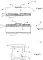
- FIG. 6 is a top plan schematic view of a prior art diode that illustrates this point.
- the overall diode is broadly designated at 40 and includes a sapphire (Al 2 O 3 ) substrate 41.
- Sapphire is used as the substrate in a number of types of light emitting diodes because of its generally rugged physical characteristics and satisfactory optical properties. Its crystal lattice is also a satisfactory, although not necessarily optimal, match with the crystal lattice of the Group III nitrides typically used to form blue light emitting diodes. Sapphire, however, cannot be conductively doped and thus always functions as an electrical insulator. As a result, a structure such as the one illustrated in Figure 6 must necessarily be adopted when sapphire is selected as the substrate.
- the active layers are grown on the sapphire substrate 41 to form the p-n junction for current injection purposes. Because the sapphire substrate 41 is insulating, however, the wire bond pads 44 and 45 must both face the top of the device in the manner illustrated in Figure 6 . Thus, consistent with the definitions used herein, the area of the diode 40 (for purposes of measuring and expressing output per unit area) is the area of the sapphire substrate rather than merely the area of the active layer 42 or the smaller active layer 43.
- the area is the larger of either (i) the largest semiconductor area in the diode or (ii) the substrate area of the diode that must or will be packaged. In almost all circumstances, area (ii) is greater or equal to area (i).
- Figures 3 , 4 and 5 are additional structural embodiments of diodes not comprised by the present invention.
- the diode is broadly designated at 50 and is shown in a "flip chip: orientation; i.e., the silicon carbide substrate 51 is in a top or upper arrangement when the diode 50 is mounted for use.
- the substrate 51 includes the oblique surfaces 52 that can increase the light output from the device by reducing total internal reflection.
- the active layers are, for purposes of simplicity, illustrated as the single layer 53 but it will be understood, that the active structure usually includes at least one p-type and one n-type layer and potentially more sophisticated structures such as quantum wells, multiple quantum wells, and superlattice structures.
- the diode 50 preferably includes the mirror layer 54 which, if formed of silver, is preferably partially isolated in the manner previously discussed with respect to Figure 1 . If formed of a less reactive metal, or one less likely to migrate, the mirror layer 54 can be a simple coating as illustrated in Figure 3 . In Figure 3 , the mirror layer 54 also forms the ohmic contact.
- Figure 4 illustrates a device otherwise similar to Figure 3 and broadly designated at 60.
- the only relevant difference between the diode 60 of Figure 4 and the diode 50 of Figure 3 is in the shape of the sidewalls 62 which are perpendicular, or nearly so, to the top surface of the device 60.
- the slightly differently shaped substrate is designated at 61, but all of the other elements are otherwise identical in structure and function to the same elements in Figure 3 , and thus carry the same reference numerals.
- the active layer is designated at 53, the mirror-contact at 54, the top ohmic contact at 56 and the bonding metal at 55.
- the light emitting surfaces of the diode 60 can be formed into lenticular shapes or patterns that can help increase the light extraction from the diode.
- the use of lenticular surfaces for this purpose is set forth in the parent application herein, and other means of varying the surface for light extraction are likewise set forth in commonly-assigned U.S. Patent No. 6,791,119 .
- Figure 5 illustrates another embodiment not comprised by the invention in which the active layer(s) 66 is positioned at the top of the device and in direct contact with an ohmic contact 67.
- the mirror-ohmic contact 70 is beneath the active layer 66 to increase the light extraction and a metal bonding layer 71 is optionally included to attach the active layer 66 and the mirror 70 to the substrate 72 which can be a semiconductor such as silicon carbide or potentially a conductor.
- An ohmic contact 73 to the substrate 72 completes the device. If the mirror-contact 70 is silver or silver-based, a barrier structure (e.g. as described with respect to Figure 1 ) would also be included.
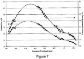
- Figure 7 is a combined plot of the spectral radiant flux output (mW, lower curve) and the external quantum efficiency (%, upper curve) for a light emitting diode not comprised in the present invention. As illustrated therein, the relative luminous flux of the diode depends upon the wavelength.
Landscapes
- Led Devices (AREA)
- Led Device Packages (AREA)
Applications Claiming Priority (3)
| Application Number | Priority Date | Filing Date | Title |
|---|---|---|---|
| US10/951,042 US7259402B2 (en) | 2004-09-22 | 2004-09-22 | High efficiency group III nitride-silicon carbide light emitting diode |
| US11/037,965 US8513686B2 (en) | 2004-09-22 | 2005-01-18 | High output small area group III nitride LEDs |
| PCT/US2005/033013 WO2006036582A1 (en) | 2004-09-22 | 2005-09-15 | High output small area group iii nitride leds |
Publications (2)
| Publication Number | Publication Date |
|---|---|
| EP1792353A1 EP1792353A1 (en) | 2007-06-06 |
| EP1792353B1 true EP1792353B1 (en) | 2020-03-11 |
Family
ID=35601712
Family Applications (1)
| Application Number | Title | Priority Date | Filing Date |
|---|---|---|---|
| EP05812300.1A Expired - Lifetime EP1792353B1 (en) | 2004-09-22 | 2005-09-15 | High output small area group iii nitride leds |
Country Status (6)
| Country | Link |
|---|---|
| US (1) | US8513686B2 (enExample) |
| EP (1) | EP1792353B1 (enExample) |
| JP (1) | JP2008514030A (enExample) |
| KR (2) | KR20090099593A (enExample) |
| TW (1) | TWI312584B (enExample) |
| WO (1) | WO2006036582A1 (enExample) |
Families Citing this family (44)
| Publication number | Priority date | Publication date | Assignee | Title |
|---|---|---|---|---|
| EP1620903B1 (en) | 2003-04-30 | 2017-08-16 | Cree, Inc. | High-power solid state light emitter package |
| US7005679B2 (en) | 2003-05-01 | 2006-02-28 | Cree, Inc. | Multiple component solid state white light |
| US7915085B2 (en) * | 2003-09-18 | 2011-03-29 | Cree, Inc. | Molded chip fabrication method |
| US7534633B2 (en) | 2004-07-02 | 2009-05-19 | Cree, Inc. | LED with substrate modifications for enhanced light extraction and method of making same |
| JP2009509339A (ja) * | 2005-09-16 | 2009-03-05 | クリー インコーポレイテッド | 炭化ケイ素パワーデバイスを有する半導体ウェハを処理する方法 |
| EP1969633B1 (en) | 2005-12-22 | 2018-08-29 | Cree, Inc. | Lighting device |
| CN102437152A (zh) | 2006-04-24 | 2012-05-02 | 克利公司 | 侧视表面安装式白光led |
| US7846391B2 (en) * | 2006-05-22 | 2010-12-07 | Lumencor, Inc. | Bioanalytical instrumentation using a light source subsystem |
| US7910945B2 (en) * | 2006-06-30 | 2011-03-22 | Cree, Inc. | Nickel tin bonding system with barrier layer for semiconductor wafers and devices |
| US8643195B2 (en) | 2006-06-30 | 2014-02-04 | Cree, Inc. | Nickel tin bonding system for semiconductor wafers and devices |
| US20080042145A1 (en) * | 2006-08-18 | 2008-02-21 | Helmut Hagleitner | Diffusion barrier for light emitting diodes |
| US7910938B2 (en) * | 2006-09-01 | 2011-03-22 | Cree, Inc. | Encapsulant profile for light emitting diodes |
| US8425271B2 (en) | 2006-09-01 | 2013-04-23 | Cree, Inc. | Phosphor position in light emitting diodes |
| US7855459B2 (en) | 2006-09-22 | 2010-12-21 | Cree, Inc. | Modified gold-tin system with increased melting temperature for wafer bonding |
| JP2010512661A (ja) * | 2006-12-11 | 2010-04-22 | ザ リージェンツ オブ ザ ユニバーシティ オブ カリフォルニア | 高特性無極性iii族窒化物光デバイスの有機金属化学気相成長法(mocvd)による成長 |
| US9178121B2 (en) * | 2006-12-15 | 2015-11-03 | Cree, Inc. | Reflective mounting substrates for light emitting diodes |
| US9024349B2 (en) | 2007-01-22 | 2015-05-05 | Cree, Inc. | Wafer level phosphor coating method and devices fabricated utilizing method |
| US9159888B2 (en) * | 2007-01-22 | 2015-10-13 | Cree, Inc. | Wafer level phosphor coating method and devices fabricated utilizing method |
| US7709811B2 (en) * | 2007-07-03 | 2010-05-04 | Conner Arlie R | Light emitting diode illumination system |
| US8098375B2 (en) | 2007-08-06 | 2012-01-17 | Lumencor, Inc. | Light emitting diode illumination system |
| DE102007046519A1 (de) * | 2007-09-28 | 2009-04-02 | Osram Opto Semiconductors Gmbh | Dünnfilm-LED mit einer Spiegelschicht und Verfahren zu deren Herstellung |
| US9041285B2 (en) | 2007-12-14 | 2015-05-26 | Cree, Inc. | Phosphor distribution in LED lamps using centrifugal force |
| US9431589B2 (en) | 2007-12-14 | 2016-08-30 | Cree, Inc. | Textured encapsulant surface in LED packages |
| TWI413453B (zh) * | 2008-11-20 | 2013-10-21 | Epistar Corp | 交流發光二極體裝置 |
| US8878219B2 (en) * | 2008-01-11 | 2014-11-04 | Cree, Inc. | Flip-chip phosphor coating method and devices fabricated utilizing method |
| KR101017395B1 (ko) * | 2008-12-24 | 2011-02-28 | 서울옵토디바이스주식회사 | 복수개의 발광셀들을 갖는 발광 소자 및 그것을 제조하는 방법 |
| US8242462B2 (en) | 2009-01-23 | 2012-08-14 | Lumencor, Inc. | Lighting design of high quality biomedical devices |
| US10546846B2 (en) | 2010-07-23 | 2020-01-28 | Cree, Inc. | Light transmission control for masking appearance of solid state light sources |
| US8362458B2 (en) * | 2010-12-27 | 2013-01-29 | Industrial Technology Research Institute | Nitirde semiconductor light emitting diode |
| US8466436B2 (en) | 2011-01-14 | 2013-06-18 | Lumencor, Inc. | System and method for metered dosage illumination in a bioanalysis or other system |
| US8389957B2 (en) | 2011-01-14 | 2013-03-05 | Lumencor, Inc. | System and method for metered dosage illumination in a bioanalysis or other system |
| US9166126B2 (en) | 2011-01-31 | 2015-10-20 | Cree, Inc. | Conformally coated light emitting devices and methods for providing the same |
| US9642515B2 (en) | 2012-01-20 | 2017-05-09 | Lumencor, Inc. | Solid state continuous white light source |
| US9217561B2 (en) | 2012-06-15 | 2015-12-22 | Lumencor, Inc. | Solid state light source for photocuring |
| CN104241262B (zh) | 2013-06-14 | 2020-11-06 | 惠州科锐半导体照明有限公司 | 发光装置以及显示装置 |
| US10971612B2 (en) | 2019-06-13 | 2021-04-06 | Cree, Inc. | High electron mobility transistors and power amplifiers including said transistors having improved performance and reliability |
| US10923585B2 (en) | 2019-06-13 | 2021-02-16 | Cree, Inc. | High electron mobility transistors having improved contact spacing and/or improved contact vias |
| US11769768B2 (en) | 2020-06-01 | 2023-09-26 | Wolfspeed, Inc. | Methods for pillar connection on frontside and passive device integration on backside of die |
| US12015075B2 (en) | 2021-05-20 | 2024-06-18 | Macom Technology Solutions Holdings, Inc. | Methods of manufacturing high electron mobility transistors having a modified interface region |
| US12446252B2 (en) | 2021-05-20 | 2025-10-14 | Macom Technology Solutions Holdings, Inc. | Transistors including semiconductor surface modification and related fabrication methods |
| US12009417B2 (en) | 2021-05-20 | 2024-06-11 | Macom Technology Solutions Holdings, Inc. | High electron mobility transistors having improved performance |
| US11842937B2 (en) | 2021-07-30 | 2023-12-12 | Wolfspeed, Inc. | Encapsulation stack for improved humidity performance and related fabrication methods |
| US12218202B2 (en) | 2021-09-16 | 2025-02-04 | Wolfspeed, Inc. | Semiconductor device incorporating a substrate recess |
| TWI887662B (zh) * | 2022-06-01 | 2025-06-21 | 美商科銳Led公司 | 用於減少接合金屬之空洞的發光二極體晶片中的接觸結構 |
Citations (1)
| Publication number | Priority date | Publication date | Assignee | Title |
|---|---|---|---|---|
| WO2004010509A2 (en) * | 2002-07-22 | 2004-01-29 | Cree, Inc. | Light emitting diode including barrier layers and manufacturing methods therefor |
Family Cites Families (60)
| Publication number | Priority date | Publication date | Assignee | Title |
|---|---|---|---|---|
| US465809A (en) * | 1891-12-22 | Electrical testing-instrument | ||
| US2001622A (en) * | 1930-10-27 | 1935-05-14 | David G Mccaa | Method of and means for reducing electrical disturbances |
| FR2554606B1 (fr) * | 1983-11-04 | 1987-04-10 | Thomson Csf | Dispositif optique de concentration du rayonnement lumineux emis par une diode electroluminescente, et diode electroluminescente comportant un tel dispositif |
| JPS6159886A (ja) | 1984-08-31 | 1986-03-27 | Fujitsu Ltd | 光半導体装置の製造方法 |
| JPH0770755B2 (ja) * | 1988-01-21 | 1995-07-31 | 三菱化学株式会社 | 高輝度led用エピタキシャル基板及びその製造方法 |
| US4912532A (en) * | 1988-08-26 | 1990-03-27 | Hewlett-Packard Company | Electro-optical device with inverted transparent substrate and method for making same |
| US5103271A (en) * | 1989-09-28 | 1992-04-07 | Kabushiki Kaisha Toshiba | Semiconductor light emitting device and method of fabricating the same |
| US5300788A (en) * | 1991-01-18 | 1994-04-05 | Kopin Corporation | Light emitting diode bars and arrays and method of making same |
| US5376580A (en) * | 1993-03-19 | 1994-12-27 | Hewlett-Packard Company | Wafer bonding of light emitting diode layers |
| US5416342A (en) * | 1993-06-23 | 1995-05-16 | Cree Research, Inc. | Blue light-emitting diode with high external quantum efficiency |
| US5592501A (en) * | 1994-09-20 | 1997-01-07 | Cree Research, Inc. | Low-strain laser structures with group III nitride active layers |
| US5631190A (en) * | 1994-10-07 | 1997-05-20 | Cree Research, Inc. | Method for producing high efficiency light-emitting diodes and resulting diode structures |
| US5739554A (en) * | 1995-05-08 | 1998-04-14 | Cree Research, Inc. | Double heterojunction light emitting diode with gallium nitride active layer |
| US5985687A (en) * | 1996-04-12 | 1999-11-16 | The Regents Of The University Of California | Method for making cleaved facets for lasers fabricated with gallium nitride and other noncubic materials |
| DE19640594B4 (de) * | 1996-10-01 | 2016-08-04 | Osram Gmbh | Bauelement |
| US6825501B2 (en) * | 1997-08-29 | 2004-11-30 | Cree, Inc. | Robust Group III light emitting diode for high reliability in standard packaging applications |
| TW393785B (en) * | 1997-09-19 | 2000-06-11 | Siemens Ag | Method to produce many semiconductor-bodies |
| US6201262B1 (en) * | 1997-10-07 | 2001-03-13 | Cree, Inc. | Group III nitride photonic devices on silicon carbide substrates with conductive buffer interlay structure |
| US6071795A (en) * | 1998-01-23 | 2000-06-06 | The Regents Of The University Of California | Separation of thin films from transparent substrates by selective optical processing |
| JPH11238913A (ja) | 1998-02-20 | 1999-08-31 | Namiki Precision Jewel Co Ltd | 半導体発光デバイスチップ |
| US6459100B1 (en) * | 1998-09-16 | 2002-10-01 | Cree, Inc. | Vertical geometry ingan LED |
| JP3525061B2 (ja) * | 1998-09-25 | 2004-05-10 | 株式会社東芝 | 半導体発光素子の製造方法 |
| US6744800B1 (en) * | 1998-12-30 | 2004-06-01 | Xerox Corporation | Method and structure for nitride based laser diode arrays on an insulating substrate |
| US6320206B1 (en) * | 1999-02-05 | 2001-11-20 | Lumileds Lighting, U.S., Llc | Light emitting devices having wafer bonded aluminum gallium indium nitride structures and mirror stacks |
| US20010042866A1 (en) * | 1999-02-05 | 2001-11-22 | Carrie Carter Coman | Inxalygazn optical emitters fabricated via substrate removal |
| US6258699B1 (en) * | 1999-05-10 | 2001-07-10 | Visual Photonics Epitaxy Co., Ltd. | Light emitting diode with a permanent subtrate of transparent glass or quartz and the method for manufacturing the same |
| US6465809B1 (en) | 1999-06-09 | 2002-10-15 | Kabushiki Kaisha Toshiba | Bonding type semiconductor substrate, semiconductor light emitting element, and preparation process thereof |
| US6812053B1 (en) * | 1999-10-14 | 2004-11-02 | Cree, Inc. | Single step pendeo- and lateral epitaxial overgrowth of Group III-nitride epitaxial layers with Group III-nitride buffer layer and resulting structures |
| US6410942B1 (en) * | 1999-12-03 | 2002-06-25 | Cree Lighting Company | Enhanced light extraction through the use of micro-LED arrays |
| AU4139101A (en) * | 1999-12-03 | 2001-06-12 | Cree Lighting Company | Enhanced light extraction in leds through the use of internal and external optical elements |
| US20020068373A1 (en) * | 2000-02-16 | 2002-06-06 | Nova Crystals, Inc. | Method for fabricating light emitting diodes |
| DE10008583A1 (de) * | 2000-02-24 | 2001-09-13 | Osram Opto Semiconductors Gmbh | Verfahren zum Herstellen eines optisch transparenten Substrates und Verfahren zum Herstellen eines lichtemittierenden Halbleiterchips |
| US6335263B1 (en) * | 2000-03-22 | 2002-01-01 | The Regents Of The University Of California | Method of forming a low temperature metal bond for use in the transfer of bulk and thin film materials |
| JP4060511B2 (ja) * | 2000-03-28 | 2008-03-12 | パイオニア株式会社 | 窒化物半導体素子の分離方法 |
| DE10051465A1 (de) * | 2000-10-17 | 2002-05-02 | Osram Opto Semiconductors Gmbh | Verfahren zur Herstellung eines Halbleiterbauelements auf GaN-Basis |
| US6410940B1 (en) * | 2000-06-15 | 2002-06-25 | Kansas State University Research Foundation | Micro-size LED and detector arrays for minidisplay, hyper-bright light emitting diodes, lighting, and UV detector and imaging sensor applications |
| DE10033496A1 (de) * | 2000-07-10 | 2002-01-31 | Osram Opto Semiconductors Gmbh | Halbleiterchip für die Optoelektronik |
| US6562648B1 (en) * | 2000-08-23 | 2003-05-13 | Xerox Corporation | Structure and method for separation and transfer of semiconductor thin films onto dissimilar substrate materials |
| DE10042947A1 (de) * | 2000-08-31 | 2002-03-21 | Osram Opto Semiconductors Gmbh | Strahlungsemittierendes Halbleiterbauelement auf GaN-Basis |
| JP4091261B2 (ja) * | 2000-10-31 | 2008-05-28 | 株式会社東芝 | 半導体発光素子及びその製造方法 |
| US6800876B2 (en) * | 2001-01-16 | 2004-10-05 | Cree, Inc. | Group III nitride LED with undoped cladding layer (5000.137) |
| US6791119B2 (en) * | 2001-02-01 | 2004-09-14 | Cree, Inc. | Light emitting diodes including modifications for light extraction |
| US6468824B2 (en) * | 2001-03-22 | 2002-10-22 | Uni Light Technology Inc. | Method for forming a semiconductor device having a metallic substrate |
| EP1263058B1 (en) | 2001-05-29 | 2012-04-18 | Toyoda Gosei Co., Ltd. | Light-emitting element |
| JP2002368263A (ja) * | 2001-06-06 | 2002-12-20 | Toyoda Gosei Co Ltd | Iii族窒化物系化合物半導体発光素子 |
| EP2034530B1 (en) * | 2001-06-15 | 2015-01-21 | Cree, Inc. | GaN based LED formed on a SiC substrate |
| US6747298B2 (en) * | 2001-07-23 | 2004-06-08 | Cree, Inc. | Collets for bonding of light emitting diodes having shaped substrates |
| US6888167B2 (en) * | 2001-07-23 | 2005-05-03 | Cree, Inc. | Flip-chip bonding of light emitting devices and light emitting devices suitable for flip-chip bonding |
| US6740906B2 (en) * | 2001-07-23 | 2004-05-25 | Cree, Inc. | Light emitting diodes including modifications for submount bonding |
| US6924596B2 (en) * | 2001-11-01 | 2005-08-02 | Nichia Corporation | Light emitting apparatus provided with fluorescent substance and semiconductor light emitting device, and method of manufacturing the same |
| US6635503B2 (en) * | 2002-01-28 | 2003-10-21 | Cree, Inc. | Cluster packaging of light emitting diodes |
| US6716654B2 (en) * | 2002-03-12 | 2004-04-06 | Opto Tech Corporation | Light-emitting diode with enhanced brightness and method for fabricating the same |
| US20040012027A1 (en) * | 2002-06-13 | 2004-01-22 | Cree Lighting Company | Saturated phosphor solid state emitter |
| US6649437B1 (en) * | 2002-08-20 | 2003-11-18 | United Epitaxy Company, Ltd. | Method of manufacturing high-power light emitting diodes |
| US6917057B2 (en) * | 2002-12-31 | 2005-07-12 | Gelcore Llc | Layered phosphor coatings for LED devices |
| US6825559B2 (en) * | 2003-01-02 | 2004-11-30 | Cree, Inc. | Group III nitride based flip-chip intergrated circuit and method for fabricating |
| TWI226138B (en) * | 2003-01-03 | 2005-01-01 | Super Nova Optoelectronics Cor | GaN-based LED vertical device structure and the manufacturing method thereof |
| US6786390B2 (en) * | 2003-02-04 | 2004-09-07 | United Epitaxy Company Ltd. | LED stack manufacturing method and its structure thereof |
| US6806112B1 (en) * | 2003-09-22 | 2004-10-19 | National Chung-Hsing University | High brightness light emitting diode |
| KR100609117B1 (ko) * | 2005-05-03 | 2006-08-08 | 삼성전기주식회사 | 질화물계 반도체 발광소자 및 그 제조방법 |
-
2005
- 2005-01-18 US US11/037,965 patent/US8513686B2/en not_active Expired - Lifetime
- 2005-09-15 KR KR1020097017902A patent/KR20090099593A/ko not_active Ceased
- 2005-09-15 JP JP2007533549A patent/JP2008514030A/ja active Pending
- 2005-09-15 EP EP05812300.1A patent/EP1792353B1/en not_active Expired - Lifetime
- 2005-09-15 TW TW094131892A patent/TWI312584B/zh not_active IP Right Cessation
- 2005-09-15 KR KR1020077006473A patent/KR20070046182A/ko not_active Ceased
- 2005-09-15 WO PCT/US2005/033013 patent/WO2006036582A1/en not_active Ceased
Patent Citations (1)
| Publication number | Priority date | Publication date | Assignee | Title |
|---|---|---|---|---|
| WO2004010509A2 (en) * | 2002-07-22 | 2004-01-29 | Cree, Inc. | Light emitting diode including barrier layers and manufacturing methods therefor |
Also Published As
| Publication number | Publication date |
|---|---|
| TW200625690A (en) | 2006-07-16 |
| EP1792353A1 (en) | 2007-06-06 |
| KR20070046182A (ko) | 2007-05-02 |
| TWI312584B (en) | 2009-07-21 |
| US8513686B2 (en) | 2013-08-20 |
| JP2008514030A (ja) | 2008-05-01 |
| US20060060879A1 (en) | 2006-03-23 |
| KR20090099593A (ko) | 2009-09-22 |
| WO2006036582A1 (en) | 2006-04-06 |
Similar Documents
| Publication | Publication Date | Title |
|---|---|---|
| EP1792353B1 (en) | High output small area group iii nitride leds | |
| CN100530713C (zh) | 高输出小面积第ⅲ族氮化物led | |
| US7737459B2 (en) | High output group III nitride light emitting diodes | |
| JP4101468B2 (ja) | 発光装置の製造方法 | |
| US8288942B2 (en) | High efficacy white LED | |
| US7213942B2 (en) | Light emitting diodes for high AC voltage operation and general lighting | |
| US7804099B2 (en) | Solid-state light source | |
| CN1819255B (zh) | 基于微型发光二极管的高压交直流指示灯 | |
| US11510294B2 (en) | Lumiphoric arrangements for light emitting diode packages | |
| US8178888B2 (en) | Semiconductor light emitting devices with high color rendering | |
| CN109429532A (zh) | 发光器件封装和光源设备 | |
| WO2020263748A1 (en) | Light emitting diode packages | |
| CN109757120A (zh) | 发光器件封装 | |
| WO2006127030A1 (en) | High efficacy white led | |
| KR101723540B1 (ko) | 발광 소자 및 이를 갖는 발광 소자 패키지 | |
| KR20180090529A (ko) | 반도체 소자 패키지 | |
| KR102131309B1 (ko) | 형광체 및 이를 포함하는 발광소자 패키지 | |
| US11101250B2 (en) | Light-emitting device package | |
| KR102509064B1 (ko) | 발광소자 패키지 및 이를 포함하는 조명장치 | |
| KR20170135381A (ko) | 반도체 소자 패키지 | |
| KR20170044316A (ko) | 발광소자 및 이를 포함하는 발광소자 패키지 |
Legal Events
| Date | Code | Title | Description |
|---|---|---|---|
| PUAI | Public reference made under article 153(3) epc to a published international application that has entered the european phase |
Free format text: ORIGINAL CODE: 0009012 |
|
| 17P | Request for examination filed |
Effective date: 20070306 |
|
| AK | Designated contracting states |
Kind code of ref document: A1 Designated state(s): AT BE BG CH CY CZ DE DK EE ES FI FR GB GR HU IE IS IT LI LT LU LV MC NL PL PT RO SE SI SK TR |
|
| 17Q | First examination report despatched |
Effective date: 20070813 |
|
| DAX | Request for extension of the european patent (deleted) | ||
| STAA | Information on the status of an ep patent application or granted ep patent |
Free format text: STATUS: EXAMINATION IS IN PROGRESS |
|
| RIC1 | Information provided on ipc code assigned before grant |
Ipc: H01L 33/40 20100101ALI20190919BHEP Ipc: H01L 27/15 20060101ALI20190919BHEP Ipc: H01L 33/32 20100101ALI20190919BHEP Ipc: H01L 33/00 20100101AFI20190919BHEP Ipc: H01L 33/20 20100101ALI20190919BHEP |
|
| GRAP | Despatch of communication of intention to grant a patent |
Free format text: ORIGINAL CODE: EPIDOSNIGR1 |
|
| STAA | Information on the status of an ep patent application or granted ep patent |
Free format text: STATUS: GRANT OF PATENT IS INTENDED |
|
| INTG | Intention to grant announced |
Effective date: 20191108 |
|
| GRAS | Grant fee paid |
Free format text: ORIGINAL CODE: EPIDOSNIGR3 |
|
| GRAA | (expected) grant |
Free format text: ORIGINAL CODE: 0009210 |
|
| STAA | Information on the status of an ep patent application or granted ep patent |
Free format text: STATUS: THE PATENT HAS BEEN GRANTED |
|
| REG | Reference to a national code |
Ref country code: DE Ref legal event code: R081 Ref document number: 602005056685 Country of ref document: DE Owner name: CREELED, INC., NEWARK, US Free format text: FORMER OWNER: CREE, INC., DURHAM, N.C., US |
|
| AK | Designated contracting states |
Kind code of ref document: B1 Designated state(s): AT BE BG CH CY CZ DE DK EE ES FI FR GB GR HU IE IS IT LI LT LU LV MC NL PL PT RO SE SI SK TR |
|
| REG | Reference to a national code |
Ref country code: GB Ref legal event code: FG4D |
|
| REG | Reference to a national code |
Ref country code: CH Ref legal event code: EP |
|
| REG | Reference to a national code |
Ref country code: AT Ref legal event code: REF Ref document number: 1244243 Country of ref document: AT Kind code of ref document: T Effective date: 20200315 |
|
| REG | Reference to a national code |
Ref country code: DE Ref legal event code: R096 Ref document number: 602005056685 Country of ref document: DE |
|
| REG | Reference to a national code |
Ref country code: IE Ref legal event code: FG4D |
|
| PG25 | Lapsed in a contracting state [announced via postgrant information from national office to epo] |
Ref country code: FI Free format text: LAPSE BECAUSE OF FAILURE TO SUBMIT A TRANSLATION OF THE DESCRIPTION OR TO PAY THE FEE WITHIN THE PRESCRIBED TIME-LIMIT Effective date: 20200311 |
|
| REG | Reference to a national code |
Ref country code: NL Ref legal event code: MP Effective date: 20200311 |
|
| PG25 | Lapsed in a contracting state [announced via postgrant information from national office to epo] |
Ref country code: GR Free format text: LAPSE BECAUSE OF FAILURE TO SUBMIT A TRANSLATION OF THE DESCRIPTION OR TO PAY THE FEE WITHIN THE PRESCRIBED TIME-LIMIT Effective date: 20200612 Ref country code: BG Free format text: LAPSE BECAUSE OF FAILURE TO SUBMIT A TRANSLATION OF THE DESCRIPTION OR TO PAY THE FEE WITHIN THE PRESCRIBED TIME-LIMIT Effective date: 20200611 Ref country code: SE Free format text: LAPSE BECAUSE OF FAILURE TO SUBMIT A TRANSLATION OF THE DESCRIPTION OR TO PAY THE FEE WITHIN THE PRESCRIBED TIME-LIMIT Effective date: 20200311 Ref country code: LV Free format text: LAPSE BECAUSE OF FAILURE TO SUBMIT A TRANSLATION OF THE DESCRIPTION OR TO PAY THE FEE WITHIN THE PRESCRIBED TIME-LIMIT Effective date: 20200311 |
|
| REG | Reference to a national code |
Ref country code: LT Ref legal event code: MG4D |
|
| PG25 | Lapsed in a contracting state [announced via postgrant information from national office to epo] |
Ref country code: NL Free format text: LAPSE BECAUSE OF FAILURE TO SUBMIT A TRANSLATION OF THE DESCRIPTION OR TO PAY THE FEE WITHIN THE PRESCRIBED TIME-LIMIT Effective date: 20200311 |
|
| PG25 | Lapsed in a contracting state [announced via postgrant information from national office to epo] |
Ref country code: PT Free format text: LAPSE BECAUSE OF FAILURE TO SUBMIT A TRANSLATION OF THE DESCRIPTION OR TO PAY THE FEE WITHIN THE PRESCRIBED TIME-LIMIT Effective date: 20200805 Ref country code: IS Free format text: LAPSE BECAUSE OF FAILURE TO SUBMIT A TRANSLATION OF THE DESCRIPTION OR TO PAY THE FEE WITHIN THE PRESCRIBED TIME-LIMIT Effective date: 20200711 Ref country code: RO Free format text: LAPSE BECAUSE OF FAILURE TO SUBMIT A TRANSLATION OF THE DESCRIPTION OR TO PAY THE FEE WITHIN THE PRESCRIBED TIME-LIMIT Effective date: 20200311 Ref country code: CZ Free format text: LAPSE BECAUSE OF FAILURE TO SUBMIT A TRANSLATION OF THE DESCRIPTION OR TO PAY THE FEE WITHIN THE PRESCRIBED TIME-LIMIT Effective date: 20200311 Ref country code: EE Free format text: LAPSE BECAUSE OF FAILURE TO SUBMIT A TRANSLATION OF THE DESCRIPTION OR TO PAY THE FEE WITHIN THE PRESCRIBED TIME-LIMIT Effective date: 20200311 Ref country code: LT Free format text: LAPSE BECAUSE OF FAILURE TO SUBMIT A TRANSLATION OF THE DESCRIPTION OR TO PAY THE FEE WITHIN THE PRESCRIBED TIME-LIMIT Effective date: 20200311 Ref country code: SK Free format text: LAPSE BECAUSE OF FAILURE TO SUBMIT A TRANSLATION OF THE DESCRIPTION OR TO PAY THE FEE WITHIN THE PRESCRIBED TIME-LIMIT Effective date: 20200311 |
|
| REG | Reference to a national code |
Ref country code: AT Ref legal event code: MK05 Ref document number: 1244243 Country of ref document: AT Kind code of ref document: T Effective date: 20200311 |
|
| REG | Reference to a national code |
Ref country code: DE Ref legal event code: R097 Ref document number: 602005056685 Country of ref document: DE |
|
| PLBE | No opposition filed within time limit |
Free format text: ORIGINAL CODE: 0009261 |
|
| STAA | Information on the status of an ep patent application or granted ep patent |
Free format text: STATUS: NO OPPOSITION FILED WITHIN TIME LIMIT |
|
| PG25 | Lapsed in a contracting state [announced via postgrant information from national office to epo] |
Ref country code: ES Free format text: LAPSE BECAUSE OF FAILURE TO SUBMIT A TRANSLATION OF THE DESCRIPTION OR TO PAY THE FEE WITHIN THE PRESCRIBED TIME-LIMIT Effective date: 20200311 Ref country code: IT Free format text: LAPSE BECAUSE OF FAILURE TO SUBMIT A TRANSLATION OF THE DESCRIPTION OR TO PAY THE FEE WITHIN THE PRESCRIBED TIME-LIMIT Effective date: 20200311 Ref country code: AT Free format text: LAPSE BECAUSE OF FAILURE TO SUBMIT A TRANSLATION OF THE DESCRIPTION OR TO PAY THE FEE WITHIN THE PRESCRIBED TIME-LIMIT Effective date: 20200311 Ref country code: DK Free format text: LAPSE BECAUSE OF FAILURE TO SUBMIT A TRANSLATION OF THE DESCRIPTION OR TO PAY THE FEE WITHIN THE PRESCRIBED TIME-LIMIT Effective date: 20200311 |
|
| 26N | No opposition filed |
Effective date: 20201214 |
|
| PG25 | Lapsed in a contracting state [announced via postgrant information from national office to epo] |
Ref country code: PL Free format text: LAPSE BECAUSE OF FAILURE TO SUBMIT A TRANSLATION OF THE DESCRIPTION OR TO PAY THE FEE WITHIN THE PRESCRIBED TIME-LIMIT Effective date: 20200311 Ref country code: SI Free format text: LAPSE BECAUSE OF FAILURE TO SUBMIT A TRANSLATION OF THE DESCRIPTION OR TO PAY THE FEE WITHIN THE PRESCRIBED TIME-LIMIT Effective date: 20200311 |
|
| PG25 | Lapsed in a contracting state [announced via postgrant information from national office to epo] |
Ref country code: MC Free format text: LAPSE BECAUSE OF FAILURE TO SUBMIT A TRANSLATION OF THE DESCRIPTION OR TO PAY THE FEE WITHIN THE PRESCRIBED TIME-LIMIT Effective date: 20200311 |
|
| REG | Reference to a national code |
Ref country code: CH Ref legal event code: PL |
|
| GBPC | Gb: european patent ceased through non-payment of renewal fee |
Effective date: 20200915 |
|
| REG | Reference to a national code |
Ref country code: BE Ref legal event code: MM Effective date: 20200930 |
|
| PG25 | Lapsed in a contracting state [announced via postgrant information from national office to epo] |
Ref country code: LU Free format text: LAPSE BECAUSE OF NON-PAYMENT OF DUE FEES Effective date: 20200915 |
|
| REG | Reference to a national code |
Ref country code: DE Ref legal event code: R082 Ref document number: 602005056685 Country of ref document: DE Representative=s name: ISARPATENT - PATENT- UND RECHTSANWAELTE BARTH , DE Ref country code: DE Ref legal event code: R081 Ref document number: 602005056685 Country of ref document: DE Owner name: CREELED, INC., NEWARK, US Free format text: FORMER OWNER: CREE, INC., DURHAM, N.C., US |
|
| PG25 | Lapsed in a contracting state [announced via postgrant information from national office to epo] |
Ref country code: FR Free format text: LAPSE BECAUSE OF NON-PAYMENT OF DUE FEES Effective date: 20200930 |
|
| PG25 | Lapsed in a contracting state [announced via postgrant information from national office to epo] |
Ref country code: GB Free format text: LAPSE BECAUSE OF NON-PAYMENT OF DUE FEES Effective date: 20200915 Ref country code: LI Free format text: LAPSE BECAUSE OF NON-PAYMENT OF DUE FEES Effective date: 20200930 Ref country code: IE Free format text: LAPSE BECAUSE OF NON-PAYMENT OF DUE FEES Effective date: 20200915 Ref country code: BE Free format text: LAPSE BECAUSE OF NON-PAYMENT OF DUE FEES Effective date: 20200930 Ref country code: CH Free format text: LAPSE BECAUSE OF NON-PAYMENT OF DUE FEES Effective date: 20200930 |
|
| PG25 | Lapsed in a contracting state [announced via postgrant information from national office to epo] |
Ref country code: TR Free format text: LAPSE BECAUSE OF FAILURE TO SUBMIT A TRANSLATION OF THE DESCRIPTION OR TO PAY THE FEE WITHIN THE PRESCRIBED TIME-LIMIT Effective date: 20200311 Ref country code: CY Free format text: LAPSE BECAUSE OF FAILURE TO SUBMIT A TRANSLATION OF THE DESCRIPTION OR TO PAY THE FEE WITHIN THE PRESCRIBED TIME-LIMIT Effective date: 20200311 |
|
| P01 | Opt-out of the competence of the unified patent court (upc) registered |
Effective date: 20230530 |
|
| PGFP | Annual fee paid to national office [announced via postgrant information from national office to epo] |
Ref country code: DE Payment date: 20240927 Year of fee payment: 20 |
|
| REG | Reference to a national code |
Ref country code: DE Ref legal event code: R079 Ref document number: 602005056685 Country of ref document: DE Free format text: PREVIOUS MAIN CLASS: H01L0033000000 Ipc: H10H0020000000 |
|
| REG | Reference to a national code |
Ref country code: DE Ref legal event code: R071 Ref document number: 602005056685 Country of ref document: DE |