EP1788595B1 - Festkondensator und dessen Herstellungsverfahren - Google Patents
Festkondensator und dessen Herstellungsverfahren Download PDFInfo
- Publication number
- EP1788595B1 EP1788595B1 EP05025181A EP05025181A EP1788595B1 EP 1788595 B1 EP1788595 B1 EP 1788595B1 EP 05025181 A EP05025181 A EP 05025181A EP 05025181 A EP05025181 A EP 05025181A EP 1788595 B1 EP1788595 B1 EP 1788595B1
- Authority
- EP
- European Patent Office
- Prior art keywords
- dielectric layer
- loose
- solid capacitor
- dielectric
- dense
- Prior art date
- Legal status (The legal status is an assumption and is not a legal conclusion. Google has not performed a legal analysis and makes no representation as to the accuracy of the status listed.)
- Not-in-force
Links
Images


Classifications
-
- H—ELECTRICITY
- H01—ELECTRIC ELEMENTS
- H01G—CAPACITORS; CAPACITORS, RECTIFIERS, DETECTORS, SWITCHING DEVICES OR LIGHT-SENSITIVE DEVICES, OF THE ELECTROLYTIC TYPE
- H01G4/00—Fixed capacitors; Processes of their manufacture
- H01G4/002—Details
- H01G4/005—Electrodes
-
- H—ELECTRICITY
- H01—ELECTRIC ELEMENTS
- H01G—CAPACITORS; CAPACITORS, RECTIFIERS, DETECTORS, SWITCHING DEVICES OR LIGHT-SENSITIVE DEVICES, OF THE ELECTROLYTIC TYPE
- H01G4/00—Fixed capacitors; Processes of their manufacture
- H01G4/002—Details
- H01G4/018—Dielectrics
- H01G4/06—Solid dielectrics
-
- H—ELECTRICITY
- H01—ELECTRIC ELEMENTS
- H01G—CAPACITORS; CAPACITORS, RECTIFIERS, DETECTORS, SWITCHING DEVICES OR LIGHT-SENSITIVE DEVICES, OF THE ELECTROLYTIC TYPE
- H01G4/00—Fixed capacitors; Processes of their manufacture
- H01G4/002—Details
- H01G4/018—Dielectrics
- H01G4/06—Solid dielectrics
- H01G4/08—Inorganic dielectrics
- H01G4/12—Ceramic dielectrics
Definitions
- the present invention relates to a capacitor, especially to a solid capacitor that increases the capacity by means of larger surface area of the dielectric layer thereof. Moreover, the solid capacitor in accordance with the present invention can be stacked repeatedly so as to form a multilayer capacitor.
- a capacitor is an energy storage component applied in circuits for tuning, filtering, coupling, by-pass, energy conversion and delay.
- Most common used capacitors are electrolytic capacitors, mica capacitors, ceramic capacitors and vitreous-enamel capacitor.
- the names refer to the type of dielectric that is used within the capacitor.
- capacitor types structure and features aluminum electrolytic and capacitor An aluminum cylinder works as a cathode with liquid electrolyte therein a curved aluminum piece is used as an anode. The flow of direct current causes an insulating metal oxide to grow out of and into the surface of the anode. The metal oxide is used as dielectric.
- the advantage of electrolytic capacitors is the high capacity per unit volume.
- the disadvantage of electrolytic capacitors is the non-ideal, lossy characteristics and poor stability.
- paper capacitor Two metal foils as electrodes are clipped on insulated paper and the assembly can be rolled up to form a cylinder that is enclosed inside a metal housing or insulated material such as sealing wax, ceramic or vitreous-enamel. The package is smaller with higher capacitance. Due to high inherent inductance and loss of capacitor, the device is suitable for being applied to low frequency circuit.
- metallized paper capacitor The device basically has the same structure with paper capacitors while a metal membrane is used instead of metal foil. Its features are small volume and higher capacitance, generally applied to low-frequency circuit. oil impregnated paper capacitor By impregnating the paper with special oil, tolerance of the capacitor is improved.
- vitreous-enamel capacitor The dielectric material is vitreous-enamel. It has advantages of ceramic capacitors while the volume is smaller. It withstands high temperature.
- ceramic capacitor The dielectric is ceramic and the plates are made from ceramic base with silver membrane. Its features are small volume, good thermostability, higher insulation resistance but low capacity. Thus it is used for high frequency circuit.
- the ferroelectric ceramic capacitor has higher capacity while the loss and temperature coefficient are higher. Thus it is applied to low frequency circuit.
- film capacitor This capacitor has the same structure with the paper capacitor.
- the dielectric of the capacitor is polyester or polystyrene. The polyester capacitor has higher dielectric constant, small volume, high capacity, and good stability thus is suitable for bypass capacitors.
- While the polystyrene capacitor has small loss, high insulation resistance but high temperature coefficient. This capacitor is suitable for high frequency circuit.
- mica capacitor The silver electrodes or metal foil are plated directly onto the mica dielectric. Several layers of electrodes and mica are laminated and then are cast inside the phenolic resin or sealed inside the epoxy. Its properties are low loss of dielectric, high insulation resistance, low temperature coefficient and it is suitable for high frequency circuit.
- tantalum or niobium electrolytic capacitor Tantalum or niobium is used as positive electrode and diluted sulfuric acid works as negative electrode while dielectric is oxide membrane on surface of the tantalum or niobium. It has small volume, high capacity, stable performance, long life, high insulation resistance, and good thermostability.
- semi-variable capacitor It's also called trimmer capacitor.
- the device consists of two pieces or two sets of metal spring with dielectric therebetween. The distance or area between two metal springs changes while tuning.
- the dielectric can be air, ceramic, mica or membrane.
- variable capacitor It is constructed by a set of immobile plates called stator, and another set of plates, connected to a common axis, called rotor and its capacity changes according to rotation of the rotor.
- the two-fold capacitors are two capacitors whose rotors share the common axis.
- the dielectric of such capacitor can be air or polystyrene. Capacitors with air dielectric with features of large volume and small loss are used in the electron tube radios.
- the variable capacitor with polystyrene dielectric is a compact sealed capacitor, mostly used in the transistor radio.
- Solid capacitors with dielectric layer made from ceramic material with high dielectric constant have features of environmental protection, low impedance, high thermostability, withstanding high ripple current and high reliability. Compared with traditional electrolytic capacitors, solid capacitors have higher stability thus explosion may occur less frequently.
- US 2003 169 555 describes a capacitor where a dielectric ceramic green tape having a conductive metal paste applied thereto is laminated and co-fired with a ceramic tape filled with a vogue material which is burnt off during firing to give a porous electrode layer precursor layer.
- An electrode layer is made therefrom by impregnating with conductive metal.
- the most common solid capacitor is multilayer ceramic capacitor (MLCC) manufactured by suspending ceramic powders in liquid and casting into a thin green sheet with thickness from 20um to 5um or even thinner. Then metal electrodes are sieved(screen) printed onto the sheets which are later stacked with sheets without electrodes alternately to form a laminated structure. After being sintered at high temperature, the device becomes a ceramic sinter that provides an extremely high capacity in a small volume. At last, surface of silver terminal electrode is plated with nickel, tin and lead and then the multilayer ceramic is soldered directly onto the printed circuit board.
- MLCC multilayer ceramic capacitor
- the present invention provides a solid capacitor that improves disadvantages of electrolytic capacitors and increases capacity.
- the capacitor includes a dielectric layer with a plurality of holes on surface thereof and two electrodes arranged on two sides of the dielectric layer respectively.
- the electrodes contact the holes. Due to the plurality of holes on surface of the dielectric layer, the surface area of the dielectric layer is increased so that the capacity of the solid capacitor is improved.
- the present invention provides a solid capacitor as defined by the features of claims 1, 25 and 34, respectively and a manufacturing method thereof as defined by the features of claim 13
- the solid capacitor is composed by a dielectric layer and two electrodes. A plurality of holes formed by an opening process is disposed on surface of the dielectric layer. The two electrodes are connected with the dielectric layer through the holes. Due to the enlarged surface area of the dielectric layer, the capacity of the capacitor is increased.
- the solid capacitor stores charge by physical means.
- the present invention provides a solid capacitor for improving disadvantages of conventional capacitors such as easily explosions and environmental pollutions by means of larger surface area for increasing stored charge.
- the solid capacitor is a device that stores the capacity of a physical system.
- a dielectric green tape 10 is sintered into a dense dielectric layer 100.
- the temperature for sintering ranges from 600 degrees Celsius to 1700 degrees Celsius.
- two sides of the dense dielectric layer 100 are coated with a plurality of dielectric 20 that is mixture of a plurality of high temperature volatile matter 30 or a plurality of conductive objects.
- the dense dielectric layer 100 and the dielectric 20 are sintered at an operating temperature of 300 to 1700 degrees so as to make the dielectric 20 form a loose dielectric layer 200.
- a plurality of holes 300 connected with the outside are formed on surface of tow sides of the loose dielectric layer 200.
- the diameter or width of the hole 300 is between 1nm ⁇ 100 ⁇ m while the range of 10nm ⁇ 10 ⁇ m is preferred. And the best range is from 5nm to 50 ⁇ m. Therefore, the loose dielectric layer 200 with large surface area is formed.
- two sides of the loose dielectric layer 200 are connected with two electrodes 400 respectively through the holes 300.
- the electrodes 400 are formed on surface of the loose dielectric layer 200 by one of electroplating, electroless plating, sputtering, spin-coating, coating, printing and chemical vapor deposition (CVD) or by combinations of above techniques.
- the density ratio of the loose dielectric layer 200 and the dense dielectric layer 100 ranges from 0.05 to 0.95 while the range between 0.1 1 and 0.9 is preferred and the best ratio ranges from 0.15 to 0.85.
- the material of the dielectric 20 and the dielectric green tape 10 can be the same or different. The material is selected from ceramic dielectric layer, high molecular dielectric layer, and glass dielectric layer or various combinations of above material.
- the holes 300 are formed on the loose dielectric layer 200, the holes 300 are connected to the outside, not the holes inside the loose dielectric layer 200 without contact the outside. Moreover, once the dielectric 20 having the high temperature volatile matter 30, the high temperature volatile matter 30 can be carbon, organics or their combinations. After being sintered, the holes 300 of the loose dielectric layer 200 is coated with the conductive substance 500, as shown in Fig. 1E .
- the conductive substance 500 can be carbon that works as an electrical connection between the electrodes 400 and the loose dielectric layer 200.
- the solid capacitor according to the present invention stores charge by physical means.
- the present invention further provides another manufacturing method to produce the solid capacitor.
- a dielectric green tape 40 including a first dielectric layer 42 and two second dielectric layers 44 is formed.
- the two second dielectric layers 44 mixed with a plurality of high temperature volatile matter 30 or a plurality of conductive objects are disposed on two sides of the first dielectric layer 42.
- the dielectric green tape 40 is sintered so as to make the first dielectric layer 42 become the dense dielectric layer 100.
- the high temperature volatile matter 30 is volatilized to form the holes 300 so that the second dielectric layers 44 form the loose dielectric layers 200.
- the first dielectric layer 42 and the second dielectric layers 44 are sintered into dense and loose structure respectively due to different material they are made from. The following manufacturing processes are the same with above descriptions.
- the high temperature volatile matter 30 can be carbon, organics or their combinations.
- the loose dielectric layer 200 is generated and the holes 300 thereon should be coated with the conductive object 500 for providing an electrical connection between the electrodes and the loose dielectric layers, as shown in Fig. 1E .
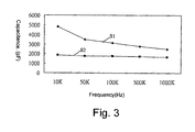
- the curves shows capacity of capacitors with or without holes under different frequencies respectively.
- the first curve S1 and the secondary curve S2 represent capacity of capacitors with and without holes respectively under different frequencies.
- the curve S 1 with the curve S2 it is obvious that the capacitor with holes has higher capacity than the capacitor without holes under different frequencies.
- a solid capacitor according to the present invention can be a multilayer capacitor for demanding of higher capacity.
- the solid capacitor 1 in accordance with the present invention is manufactured as structure in Fig. 4A , the length of two loose dielectric layers 200 of the solid capacitor 1 are shorter than that of the dense dielectric layers 100 and a first electrode 210 as well as a second electrode 220 is disposed thereof. This is a basic unit.
- a first solid capacitor 600 is arranged on a second solid capacitor 700 reversely and the second electrode 220 is electrically connected with a third electrode 710 of the second solid capacitor 700, as shown in Fig. 4B .
- a repeated unit 800 is formed.
- a first outer electrode 810 and a second outer electrode 820 are arranged on two outsides.
- the first outer electrode 810 is electrically connected with the first electrode 210 and a fourth electrode 720 of the second dielectric layer while the second outer electrode 820 is electrically connected with the second electrode 220 and the third electrode 710 so as to form a multilayer capacitor.
Claims (43)
- Feststoffkondensator, der umfasst:wenigstens eine dichte dielektrische Schicht (100);wenigstens zwei lockere dielektrische Schichten (200), die auf den zwei Außenseiten der dichten dielektrischen Schicht (100) angeordnet sind, wobei die lockeren dielektrischen Schichten (200) mehrere Löcher (300) besitzen, die mit der auf ihrer Oberfläche gebildeten Außenseite verbunden sind; undzwei Elektroden (400), die jeweils auf den Außenseiten der zwei lockeren dielektrischen Schichten (200) ausgebildet sind, wobei die Elektroden (400) mit den lockeren dielektrischen Schichten (200) durch die mehreren Löcher (300) in Kontakt sind,wobei das Verhältnis der Dichte der lockeren dielektrischen Schicht (200) zu jener der dichten dielektrischen Schicht (100) im Bereich von 0,05 bis 0,95 liegt.
- Feststoffkondensator nach Anspruch 1, wobei das Verhältnis der Dichte der lockeren dielektrischen Schicht (200) zu jener der dichten dielektrischen Schicht (100) vorzugsweise im Bereich von 0,1 bis 0,9 liegt.
- Feststoffkondensator nach Anspruch 2, wobei das Verhältnis der Dichte der lockeren dielektrischen Schicht (200) zu jener der dichten dielektrischen Schicht (100) am besten im Bereich von 0,15 bis 0,85 liegt.
- Feststoffkondensator nach Anspruch 1, wobei die lockere dielektrische Schicht (100) eine dielektrische Keramikschicht, eine dielektrische hochmolekulare Schicht, eine dielektrische Glasschicht oder eine von mehreren verschiedenen Kombinationen der obigen dielektrischen Schichten ist.
- Feststoffkondensator nach Anspruch 1, wobei die lockere dielektrische Schicht (200) eine dielektrische Keramikschicht, eine dielektrische hochmolekulare Schicht, eine dielektrische Glasschicht oder eine von mehreren verschiedenen Kombinationen der obigen dielektrischen Schichten ist.
- Feststoffkondensator nach Anspruch 1, wobei der Durchmesser oder die Weite der Löcher (300) der lockeren dielektrischen Schicht (200) im Bereich von 1 nm bis 100 µm liegt.
- Feststoffkondensator nach Anspruch 6, wobei der Durchmesser oder die Weite der Löcher (300) der lockeren dielektrischen Schicht (200) am besten im Bereich von 5 nm bis 50 µm liegt.
- Feststoffkondensator nach Anspruch 1, wobei die lockere dielektrische Schicht (200) ein Gemisch mit wenigstens einer leitenden Substanz (500) ist.
- Feststoffkondensator nach Anspruch 1, wobei die Oberfläche der Löcher (300) mit wenigstens einer leitenden Substanz (500) beschichtet ist.
- Feststoffkondensator nach Anspruch 8, wobei die leitende Substanz (500) Kohlenstoff ist.
- Feststoffkondensator nach Anspruch 9, wobei die leitende Substanz (500) Kohlenstoff ist.
- Feststoffkondensator nach Anspruch 1, wobei der Feststoffkondensator (1) Ladung auf physikalischem Weg speichert.
- Verfahren zum Herstellen eines Feststoffkondensators, das die folgenden Schritte umfasst:Bilden wenigstens einer dichten dielektrischen Schicht (100), die auf zwei Außenseiten hiervon wenigstens eine lockere dielektrische Schicht (200) und mehrere Löcher (300), die mit der Außenseite auf der Oberfläche der wenigstens einen lockeren dielektrischen Schicht (200) verbunden sind, besitzt; undBilden einer Elektrode (400) auf jeweiligen Außenseiten der lockeren dielektrischen Schicht (200), wobei die Elektrode (400) mit der lockeren dielektrischen Schicht (200) durch die Löcher (300) in Kontakt ist, und wobei das Verhältnis der Dichte der lockeren dielektrischen Schicht (200) zu jener der dichten dielektrischen Schicht (100) im Bereich von 0,05 bis 0,95 liegt.
- Herstellungsverfahren nach Anspruch 13, wobei in dem Schritt des Bildens wenigstens einer dichten dielektrischen Schicht (100), die auf ihren zwei Außenseiten jeweils wenigstens eine lockere dielektrische Schicht (200) besitzt, die lockere dielektrische Schicht (200) mit mehreren leitenden Substanzen (500) gemischt wird.
- Herstellungsverfahren nach Anspruch 13, wobei in dem Schritt des Bildens wenigstens einer dichten dielektrischen Schicht (100), die auf ihren zwei Außenseiten jeweils wenigstens eine lockere dielektrische Schicht (200) besitzt, mehrere leitende Substanzen (500) auf der Oberfläche der Löcher (300) aufgebracht sind.
- Herstellungsverfahren nach Anspruch 13, wobei der Schritt des Bildens wenigstens einer dichten dielektrischen Schicht (100), die auf ihren zwei Außenseiten jeweils wenigstens eine lockere dielektrische Schicht (200) besitzt, ferner die folgenden Schritte umfasst:Vorsehen wenigstens eines dielektrischen Rohbandes;Sintern des dielektrischen Rohbandes, um die dichte dielektrische Schicht (100) zu bilden;Aufbringen mehrerer Dielektrika auf die zwei Außenseiten der dichten dielektrischen Schicht (100); undSintern der dichten dielektrischen Schicht (100) und der Dielektrika, um zu bewirken, dass die Dielektrika die lockere dielektrische Schicht (200) bilden.
- Herstellungsverfahren nach Anspruch 16, wobei in dem Schritt des Sinterns des dielektrischen Rohbandes, um die dichte dielektrische Schicht (100) zu bilden, die Betriebstemperatur im Bereich von 600 Grad Celsius bis 1700 Grad Celsius liegt.
- Herstellungsverfahren nach Anspruch 16, wobei in dem Schritt des Sinterns der dichten dielektrischen Schicht (100) und des Dielektrikums die Betriebstemperatur im Bereich von 300 Grad Celsius bis 1700 Grad Celsius liegt.
- Herstellungsverfahren nach Anspruch 16, wobei in dem Schritt des Aufbringens mehrerer Dielektrika auf die zwei Außenseiten der dichten dielektrischen Schicht (100) das Dielektrikum mit mehreren leitenden Substanzen (500) gemischt wird.
- Herstellungsverfahren nach Anspruch 16, wobei das Verfahren ferner umfasst:nach dem Schritt des Sinterns der dichten dielektrischen Schicht (100) und des Dielektrikums, damit das Dielektrikum die lockere dielektrische Schicht (200) bildet, einen Schritt des Aufbringens mehrerer leitender Substanzen (500) auf die Oberfläche der Löcher (300) der lockeren dielektrischen Schicht (200).
- Herstellungsverfahren nach Anspruch 18, wobei der Schritt des Bildens wenigstens einer dichten dielektrischen Schicht (100), auf deren zwei Außenseiten wenigstens jeweils eine lockere dielektrische Schicht (200) vorhanden ist, ferner die folgenden Schritte umfasst:Bilden wenigstens eines dielektrischen Rohbandes (40) mit wenigstens einer ersten dielektrischen Schicht (42) und wenigstens zwei zweiten dielektrischen Schichten (44), wobei die zweiten dielektrischen Schichten (44) auf den zwei Außenseiten der ersten dielektrischen Schicht (42) angeordnet sind und die zweite dielektrische Schicht (44) mit mehreren flüchtigen Hochtemperaturstoffen (30) gemischt wird; undSintern des dielektrischen Rohbandes (40), damit die erste dielektrische Schicht (42) die dichte dielektrische Schicht (100) bildet und die flüchtigen Hochtemperaturstoffe (30) sich verflüchtigen, um die Löcher (300) zu bilden, damit die zweite dielektrische Schicht (400) die lockere dielektrische Schicht (200) wird.
- Herstellungsverfahren nach Anspruch 21, wobei in dem Schritt des Sinterns des dielektrischen Rohbandes (40) die Betriebstemperatur im Bereich von 300 Grad Celsius bis 1700 Grad Celsius liegt.
- Herstellungsverfahren nach Anspruch 21, wobei der flüchtige Hochtemperaturstoff (30) Kohlenstoff, organische Materialien oder Kombinationen aus Kohlenstoff und organischen Materialien enthält.
- Herstellungsverfahren nach Anspruch 13, wobei in dem Schritt des Bildens einer Elektrode (400) auf der jeweiligen Außenseite der losen dielektrischen Schicht (200) die Elektrode (400) auf der Außenseite der lockeren dielektrischen Schicht (200) durch Elektrobeschichtung, chemisches Beschichtung, Katodenzerstäubung, Schleuderbeschichtung, Überziehen, Drucken, Abscheiden aus der Dampfphase (CVD) oder durch Kombinationen der obigen Techniken gebildet wird.
- Feststoffkondensator, der umfasst:eine dielektrische Schicht, die wenigstens eine dichte dielektrische Schicht (100) und wenigstens zwei lockere dielektrische Schichten (200) auf den zwei Außenseiten der dichten dielektrischen Schicht (100) besitzt;mehrere Löcher (300), die mit der Außenseite verbunden sind, die auf der Oberfläche der zwei Außenseiten der lockeren dielektrischen Schichten gebildet ist; undzwei Elektroden (400), die auf den zwei Außenseiten der dielektrischen Schichten gebildet sind und mit den Löchern (300) in Kontakt sind,wobei das Verhältnis der Dichte der lockeren dielektrischen Schicht (200) zu jener der dichten dielektrischen Schicht (100) im Bereich von 0,05 bis 0,95 liegt.
- Feststoffkondensator nach Anspruch 25, wobei das Verhältnis der Dicke der jeweiligen lockeren dielektrischen Schicht (200) zu jener der dielektrischen Schicht im Bereich von 0,01 bis 0,45 liegt.
- Feststoffkondensator nach Anspruch 25, wobei das Verhältnis der Dicke der dichten dielektrischen Schicht (100) zu jener der dielektrischen Schicht im Bereich von 0,1 bis 0,98 liegt.
- Feststoffkondensator nach Anspruch 27, wobei der Durchmesser der Löcher (300) im Bereich von 0,01 nm bis 10 µm liegt.
- Feststoffkondensator nach Anspruch 25, wobei die dielektrische Schicht ein Gemisch mit mehreren leitenden Substanzen (500) ist.
- Feststoffkondensator nach Anspruch 25, wobei die Oberfläche der Löcher (300) mit mehreren leitenden Substanzen (500) beschichtet ist.
- Feststoffkondensator nach Anspruch 29, wobei die leitende Substanz (500) Kohlenstoff ist.
- Feststoffkondensator nach Anspruch 30, wobei die leitende Substanz (500) Kohlenstoff ist.
- Feststoffkondensator nach Anspruch 25, wobei der Feststoffkondensator (1) Ladung auf physikalischem Weg durch Zusammenfügen der zwei Elektroden (400) und der dielektrischen Schicht speichert.
- Feststoffkondensator, der umfasst:wenigstens eine erste dielektrische Schicht, die wenigstens eine dichte dielektrische Schicht (100) und wenigstens zwei lockere dielektrische Schichten (200), die auf den zwei Außenseiten der dichten dielektrischen Schicht (100) angeordnet sind, besitzt, wobei auf der Oberfläche ihrer zwei Außenseiten mehrere Löcher (300) ausgebildet sind, wobei die Löcher (300) mit der Außenseite verbunden sind; eine erste Elektrode (210) und eine zweite Elektrode (220) auf den Außenseiten der dielektrischen Schicht ausgebildet sind; die Elektroden (210; 220) mit den Löchern (300) in Kontakt sind; undwenigstens eine zweite dielektrische Schicht, die wenigstens eine dichte dielektrische Schicht (100) und wenigstens zwei lockere dielektrische Schichten (200), die auf den zwei Außenseiten der dichten dielektrischen Schicht (100) angeordnet sind, besitzt, wobei auf der Oberfläche ihrer zwei Außenseiten mehrere Löcher (300) ausgebildet sind, wobei die Löcher (300) mit der Außenseite verbunden sind; eine dritte Elektrode (710) und eine vierte Elektrode (720) auf den Außenseiten der dielektrischen Schicht angeordnet sind; die Elektroden mit den Löchern (300) in Kontakt sind; die zweite dielektrische Schicht umgekehrt über der ersten dielektrischen Schicht angeordnet ist, während die zweite Elektrode (220) mit der dritten Elektrode (710) in Kontakt ist;wobei der Feststoffkondensator Ladung auf physikalischem Weg speichert und das Verhältnis der Dichte der lockeren dielektrischen Schicht (200) zu jener der dichten dielektrischen Schicht (100) im Bereich von 0,05 bis 0,95 liegt.
- Feststoffkondensator nach Anspruch 34, wobei der Durchmesser der Löcher (300) im Bereich von 0,01 nm bis 10 µm liegt.
- Feststoffkondensator nach Anspruch 34, wobei die dielektrische Schicht ein Gemisch mit mehreren leitenden Substanzen (500) ist.
- Feststoffkondensator nach Anspruch 34, wobei die Oberfläche der Löcher (300) mit mehreren leitenden Substanzen (500) beschichtet ist.
- Feststoffkondensator nach Anspruch 36, wobei die leitende Substanz (500) Kohlenstoff ist.
- Feststoffkondensator nach Anspruch 37, wobei die leitende Substanz (500) Kohlenstoff ist.
- Feststoffkondensator nach Anspruch 34, wobei die Feststoffkondensatoren (600; 700) mehrfach gestapelt sind, um einen Mehrschichtkondensator (800) zu bilden.
- Feststoffkondensator nach Anspruch 40, wobei die Feststoffkondensatoren (600; 700) in einer ungeraden Anzahl gestapelt sind.
- Feststoffkondensator nach Anspruch 40, wobei die Feststoffkondensatoren (600; 700) in einer geraden Anzahl gestapelt sind.
- Feststoffkondensator nach Anspruch 40, wobei der Feststoffkondensator ferner umfasst:eine erste äußere Elektrode (810), die auf einer Seite der ersten dielektrischen Schicht und der zweiten dielektrischen Schicht angeordnet ist und mit der ersten Elektrode (210) und der vierten Elektrode (720) elektrisch verbunden ist; undeine zweite äußere Elektrode (820), die auf der anderen Seite der ersten dielektrischen Schicht und der zweiten dielektrischen Schicht angeordnet ist und mit der zweiten Elektrode (220) und mit der dritten Elektrode (710) elektrisch verbunden ist.
Priority Applications (3)
| Application Number | Priority Date | Filing Date | Title |
|---|---|---|---|
| DE602005021892T DE602005021892D1 (de) | 2005-11-17 | 2005-11-17 | Festkondensator und dessen Herstellungsverfahren |
| EP05025181A EP1788595B1 (de) | 2005-11-17 | 2005-11-17 | Festkondensator und dessen Herstellungsverfahren |
| AT05025181T ATE471569T1 (de) | 2005-11-17 | 2005-11-17 | Festkondensator und dessen herstellungsverfahren |
Applications Claiming Priority (1)
| Application Number | Priority Date | Filing Date | Title |
|---|---|---|---|
| EP05025181A EP1788595B1 (de) | 2005-11-17 | 2005-11-17 | Festkondensator und dessen Herstellungsverfahren |
Publications (2)
| Publication Number | Publication Date |
|---|---|
| EP1788595A1 EP1788595A1 (de) | 2007-05-23 |
| EP1788595B1 true EP1788595B1 (de) | 2010-06-16 |
Family
ID=36165386
Family Applications (1)
| Application Number | Title | Priority Date | Filing Date |
|---|---|---|---|
| EP05025181A Not-in-force EP1788595B1 (de) | 2005-11-17 | 2005-11-17 | Festkondensator und dessen Herstellungsverfahren |
Country Status (3)
| Country | Link |
|---|---|
| EP (1) | EP1788595B1 (de) |
| AT (1) | ATE471569T1 (de) |
| DE (1) | DE602005021892D1 (de) |
Family Cites Families (3)
| Publication number | Priority date | Publication date | Assignee | Title |
|---|---|---|---|---|
| GB1316144A (en) * | 1963-08-21 | 1973-05-09 | Mallory & Co Inc P R | Capacitor having a cooperating dielectric |
| US3679950A (en) * | 1971-04-16 | 1972-07-25 | Nl Industries Inc | Ceramic capacitors |
| US6690572B2 (en) * | 2002-03-06 | 2004-02-10 | Larry A. Liebowitz | Single layer electronic capacitors with very thin dielectrics and methods to produce same |
-
2005
- 2005-11-17 DE DE602005021892T patent/DE602005021892D1/de active Active
- 2005-11-17 EP EP05025181A patent/EP1788595B1/de not_active Not-in-force
- 2005-11-17 AT AT05025181T patent/ATE471569T1/de not_active IP Right Cessation
Also Published As
| Publication number | Publication date |
|---|---|
| DE602005021892D1 (de) | 2010-07-29 |
| EP1788595A1 (de) | 2007-05-23 |
| ATE471569T1 (de) | 2010-07-15 |
Similar Documents
| Publication | Publication Date | Title |
|---|---|---|
| US7495891B2 (en) | Solid capacitor and manufacturing method thereof | |
| US6310765B1 (en) | Electrolytic capacitor and method for manufacturing the same | |
| US8228663B2 (en) | Laminated ceramic electronic component | |
| KR100827160B1 (ko) | 적층형 고체 전해 콘덴서 | |
| US20130258546A1 (en) | Multilayer ceramic electronic component and fabrication method thereof | |
| JP5730732B2 (ja) | 積層セラミックコンデンサー及びその製造方法 | |
| CN104576056A (zh) | 多层陶瓷电容器和具有该多层陶瓷电容器的板 | |
| CN104240946A (zh) | 多层陶瓷电容器及安装有该多层陶瓷电容器的板 | |
| CN104465088A (zh) | 多层陶瓷电容器及用于安装该多层陶瓷电容器的板 | |
| US10136518B2 (en) | Multilayer ceramic capacitor having three external electrodes and board having the same | |
| KR20050008536A (ko) | 적층 세라믹 전자부품 및 그 제조방법 | |
| CN111261405B (zh) | 电容器组件 | |
| CN116168949A (zh) | 多层陶瓷电子组件 | |
| US4482933A (en) | Multilayer doped ceramic capacitor | |
| JP4428852B2 (ja) | 積層型電子部品およびその製法 | |
| CN104282436B (zh) | 多层陶瓷电容器及其制造方法以及安装电路板 | |
| JP3416053B2 (ja) | 電解コンデンサおよびその製造方法 | |
| US20120281338A1 (en) | Aluminum electrolytic capacitor and method of manfacturing the same | |
| CN111837211B (zh) | 固体电解电容器以及固体电解电容器的制造方法 | |
| EP1788595B1 (de) | Festkondensator und dessen Herstellungsverfahren | |
| CN104576049A (zh) | 多层陶瓷电子组件及其制造方法 | |
| CN100521000C (zh) | 固态电容及其制作方法 | |
| JP3519896B2 (ja) | 分極性電極およびそれを用いた電気二重層コンデンサ | |
| US20230260708A1 (en) | Multilayer electronic component | |
| KR101792407B1 (ko) | 복합 전자부품 및 그 실장 기판 |
Legal Events
| Date | Code | Title | Description |
|---|---|---|---|
| PUAI | Public reference made under article 153(3) epc to a published international application that has entered the european phase |
Free format text: ORIGINAL CODE: 0009012 |
|
| 17P | Request for examination filed |
Effective date: 20051117 |
|
| AK | Designated contracting states |
Kind code of ref document: A1 Designated state(s): AT BE BG CH CY CZ DE DK EE ES FI FR GB GR HU IE IS IT LI LT LU LV MC NL PL PT RO SE SI SK TR |
|
| AX | Request for extension of the european patent |
Extension state: AL BA HR MK YU |
|
| 17Q | First examination report despatched |
Effective date: 20070716 |
|
| AKX | Designation fees paid |
Designated state(s): AT BE BG CH CY CZ DE DK EE ES FI FR GB GR HU IE IS IT LI LT LU LV MC NL PL PT RO SE SI SK TR |
|
| GRAP | Despatch of communication of intention to grant a patent |
Free format text: ORIGINAL CODE: EPIDOSNIGR1 |
|
| GRAS | Grant fee paid |
Free format text: ORIGINAL CODE: EPIDOSNIGR3 |
|
| GRAA | (expected) grant |
Free format text: ORIGINAL CODE: 0009210 |
|
| AK | Designated contracting states |
Kind code of ref document: B1 Designated state(s): AT BE BG CH CY CZ DE DK EE ES FI FR GB GR HU IE IS IT LI LT LU LV MC NL PL PT RO SE SI SK TR |
|
| REG | Reference to a national code |
Ref country code: CH Ref legal event code: EP |
|
| REG | Reference to a national code |
Ref country code: IE Ref legal event code: FG4D |
|
| REF | Corresponds to: |
Ref document number: 602005021892 Country of ref document: DE Date of ref document: 20100729 Kind code of ref document: P |
|
| REG | Reference to a national code |
Ref country code: NL Ref legal event code: VDEP Effective date: 20100616 |
|
| PG25 | Lapsed in a contracting state [announced via postgrant information from national office to epo] |
Ref country code: SE Free format text: LAPSE BECAUSE OF FAILURE TO SUBMIT A TRANSLATION OF THE DESCRIPTION OR TO PAY THE FEE WITHIN THE PRESCRIBED TIME-LIMIT Effective date: 20100616 Ref country code: LT Free format text: LAPSE BECAUSE OF FAILURE TO SUBMIT A TRANSLATION OF THE DESCRIPTION OR TO PAY THE FEE WITHIN THE PRESCRIBED TIME-LIMIT Effective date: 20100616 |
|
| LTIE | Lt: invalidation of european patent or patent extension |
Effective date: 20100616 |
|
| PG25 | Lapsed in a contracting state [announced via postgrant information from national office to epo] |
Ref country code: SI Free format text: LAPSE BECAUSE OF FAILURE TO SUBMIT A TRANSLATION OF THE DESCRIPTION OR TO PAY THE FEE WITHIN THE PRESCRIBED TIME-LIMIT Effective date: 20100616 Ref country code: LV Free format text: LAPSE BECAUSE OF FAILURE TO SUBMIT A TRANSLATION OF THE DESCRIPTION OR TO PAY THE FEE WITHIN THE PRESCRIBED TIME-LIMIT Effective date: 20100616 Ref country code: AT Free format text: LAPSE BECAUSE OF FAILURE TO SUBMIT A TRANSLATION OF THE DESCRIPTION OR TO PAY THE FEE WITHIN THE PRESCRIBED TIME-LIMIT Effective date: 20100616 Ref country code: FI Free format text: LAPSE BECAUSE OF FAILURE TO SUBMIT A TRANSLATION OF THE DESCRIPTION OR TO PAY THE FEE WITHIN THE PRESCRIBED TIME-LIMIT Effective date: 20100616 |
|
| PG25 | Lapsed in a contracting state [announced via postgrant information from national office to epo] |
Ref country code: GR Free format text: LAPSE BECAUSE OF FAILURE TO SUBMIT A TRANSLATION OF THE DESCRIPTION OR TO PAY THE FEE WITHIN THE PRESCRIBED TIME-LIMIT Effective date: 20100917 Ref country code: PL Free format text: LAPSE BECAUSE OF FAILURE TO SUBMIT A TRANSLATION OF THE DESCRIPTION OR TO PAY THE FEE WITHIN THE PRESCRIBED TIME-LIMIT Effective date: 20100616 Ref country code: CY Free format text: LAPSE BECAUSE OF FAILURE TO SUBMIT A TRANSLATION OF THE DESCRIPTION OR TO PAY THE FEE WITHIN THE PRESCRIBED TIME-LIMIT Effective date: 20100616 |
|
| PG25 | Lapsed in a contracting state [announced via postgrant information from national office to epo] |
Ref country code: EE Free format text: LAPSE BECAUSE OF FAILURE TO SUBMIT A TRANSLATION OF THE DESCRIPTION OR TO PAY THE FEE WITHIN THE PRESCRIBED TIME-LIMIT Effective date: 20100616 Ref country code: NL Free format text: LAPSE BECAUSE OF FAILURE TO SUBMIT A TRANSLATION OF THE DESCRIPTION OR TO PAY THE FEE WITHIN THE PRESCRIBED TIME-LIMIT Effective date: 20100616 |
|
| PG25 | Lapsed in a contracting state [announced via postgrant information from national office to epo] |
Ref country code: CZ Free format text: LAPSE BECAUSE OF FAILURE TO SUBMIT A TRANSLATION OF THE DESCRIPTION OR TO PAY THE FEE WITHIN THE PRESCRIBED TIME-LIMIT Effective date: 20100616 Ref country code: BE Free format text: LAPSE BECAUSE OF FAILURE TO SUBMIT A TRANSLATION OF THE DESCRIPTION OR TO PAY THE FEE WITHIN THE PRESCRIBED TIME-LIMIT Effective date: 20100616 Ref country code: SK Free format text: LAPSE BECAUSE OF FAILURE TO SUBMIT A TRANSLATION OF THE DESCRIPTION OR TO PAY THE FEE WITHIN THE PRESCRIBED TIME-LIMIT Effective date: 20100616 Ref country code: RO Free format text: LAPSE BECAUSE OF FAILURE TO SUBMIT A TRANSLATION OF THE DESCRIPTION OR TO PAY THE FEE WITHIN THE PRESCRIBED TIME-LIMIT Effective date: 20100616 Ref country code: PT Free format text: LAPSE BECAUSE OF FAILURE TO SUBMIT A TRANSLATION OF THE DESCRIPTION OR TO PAY THE FEE WITHIN THE PRESCRIBED TIME-LIMIT Effective date: 20101018 Ref country code: IS Free format text: LAPSE BECAUSE OF FAILURE TO SUBMIT A TRANSLATION OF THE DESCRIPTION OR TO PAY THE FEE WITHIN THE PRESCRIBED TIME-LIMIT Effective date: 20101016 |
|
| PGFP | Annual fee paid to national office [announced via postgrant information from national office to epo] |
Ref country code: DE Payment date: 20101130 Year of fee payment: 6 |
|
| PGFP | Annual fee paid to national office [announced via postgrant information from national office to epo] |
Ref country code: GB Payment date: 20101124 Year of fee payment: 6 Ref country code: IT Payment date: 20101115 Year of fee payment: 6 |
|
| PLBE | No opposition filed within time limit |
Free format text: ORIGINAL CODE: 0009261 |
|
| STAA | Information on the status of an ep patent application or granted ep patent |
Free format text: STATUS: NO OPPOSITION FILED WITHIN TIME LIMIT |
|
| PG25 | Lapsed in a contracting state [announced via postgrant information from national office to epo] |
Ref country code: DK Free format text: LAPSE BECAUSE OF FAILURE TO SUBMIT A TRANSLATION OF THE DESCRIPTION OR TO PAY THE FEE WITHIN THE PRESCRIBED TIME-LIMIT Effective date: 20100616 |
|
| 26N | No opposition filed |
Effective date: 20110317 |
|
| PG25 | Lapsed in a contracting state [announced via postgrant information from national office to epo] |
Ref country code: MC Free format text: LAPSE BECAUSE OF NON-PAYMENT OF DUE FEES Effective date: 20101130 |
|
| REG | Reference to a national code |
Ref country code: CH Ref legal event code: PL |
|
| REG | Reference to a national code |
Ref country code: DE Ref legal event code: R097 Ref document number: 602005021892 Country of ref document: DE Effective date: 20110316 |
|
| PG25 | Lapsed in a contracting state [announced via postgrant information from national office to epo] |
Ref country code: LI Free format text: LAPSE BECAUSE OF NON-PAYMENT OF DUE FEES Effective date: 20101130 Ref country code: CH Free format text: LAPSE BECAUSE OF NON-PAYMENT OF DUE FEES Effective date: 20101130 |
|
| PG25 | Lapsed in a contracting state [announced via postgrant information from national office to epo] |
Ref country code: IE Free format text: LAPSE BECAUSE OF NON-PAYMENT OF DUE FEES Effective date: 20101117 |
|
| PGFP | Annual fee paid to national office [announced via postgrant information from national office to epo] |
Ref country code: FR Payment date: 20111205 Year of fee payment: 7 |
|
| PG25 | Lapsed in a contracting state [announced via postgrant information from national office to epo] |
Ref country code: BG Free format text: LAPSE BECAUSE OF FAILURE TO SUBMIT A TRANSLATION OF THE DESCRIPTION OR TO PAY THE FEE WITHIN THE PRESCRIBED TIME-LIMIT Effective date: 20100616 Ref country code: LU Free format text: LAPSE BECAUSE OF NON-PAYMENT OF DUE FEES Effective date: 20101117 Ref country code: HU Free format text: LAPSE BECAUSE OF FAILURE TO SUBMIT A TRANSLATION OF THE DESCRIPTION OR TO PAY THE FEE WITHIN THE PRESCRIBED TIME-LIMIT Effective date: 20101217 |
|
| PG25 | Lapsed in a contracting state [announced via postgrant information from national office to epo] |
Ref country code: TR Free format text: LAPSE BECAUSE OF FAILURE TO SUBMIT A TRANSLATION OF THE DESCRIPTION OR TO PAY THE FEE WITHIN THE PRESCRIBED TIME-LIMIT Effective date: 20100616 |
|
| REG | Reference to a national code |
Ref country code: DE Ref legal event code: R082 Ref document number: 602005021892 Country of ref document: DE Representative=s name: LANGPATENT ANWALTSKANZLEI IP LAW FIRM, DE |
|
| GBPC | Gb: european patent ceased through non-payment of renewal fee |
Effective date: 20121117 |
|
| REG | Reference to a national code |
Ref country code: FR Ref legal event code: ST Effective date: 20130731 |
|
| PG25 | Lapsed in a contracting state [announced via postgrant information from national office to epo] |
Ref country code: IT Free format text: LAPSE BECAUSE OF NON-PAYMENT OF DUE FEES Effective date: 20121117 |
|
| REG | Reference to a national code |
Ref country code: DE Ref legal event code: R119 Ref document number: 602005021892 Country of ref document: DE Effective date: 20130601 |
|
| PG25 | Lapsed in a contracting state [announced via postgrant information from national office to epo] |
Ref country code: BG Free format text: LAPSE BECAUSE OF FAILURE TO SUBMIT A TRANSLATION OF THE DESCRIPTION OR TO PAY THE FEE WITHIN THE PRESCRIBED TIME-LIMIT Effective date: 20100916 |
|
| PG25 | Lapsed in a contracting state [announced via postgrant information from national office to epo] |
Ref country code: DE Free format text: LAPSE BECAUSE OF NON-PAYMENT OF DUE FEES Effective date: 20130601 Ref country code: ES Free format text: LAPSE BECAUSE OF FAILURE TO SUBMIT A TRANSLATION OF THE DESCRIPTION OR TO PAY THE FEE WITHIN THE PRESCRIBED TIME-LIMIT Effective date: 20100927 |
|
| PG25 | Lapsed in a contracting state [announced via postgrant information from national office to epo] |
Ref country code: GB Free format text: LAPSE BECAUSE OF NON-PAYMENT OF DUE FEES Effective date: 20121117 Ref country code: FR Free format text: LAPSE BECAUSE OF NON-PAYMENT OF DUE FEES Effective date: 20121130 |