EP1786047A1 - Solar cell and manufacturing method of the same - Google Patents
Solar cell and manufacturing method of the same Download PDFInfo
- Publication number
- EP1786047A1 EP1786047A1 EP06123858A EP06123858A EP1786047A1 EP 1786047 A1 EP1786047 A1 EP 1786047A1 EP 06123858 A EP06123858 A EP 06123858A EP 06123858 A EP06123858 A EP 06123858A EP 1786047 A1 EP1786047 A1 EP 1786047A1
- Authority
- EP
- European Patent Office
- Prior art keywords
- electrode
- substrate
- solar cell
- mean square
- root mean
- Prior art date
- Legal status (The legal status is an assumption and is not a legal conclusion. Google has not performed a legal analysis and makes no representation as to the accuracy of the status listed.)
- Granted
Links
Images


Classifications
-
- H—ELECTRICITY
- H01—ELECTRIC ELEMENTS
- H01G—CAPACITORS; CAPACITORS, RECTIFIERS, DETECTORS, SWITCHING DEVICES, LIGHT-SENSITIVE OR TEMPERATURE-SENSITIVE DEVICES OF THE ELECTROLYTIC TYPE
- H01G9/00—Electrolytic capacitors, rectifiers, detectors, switching devices, light-sensitive or temperature-sensitive devices; Processes of their manufacture
- H01G9/20—Light-sensitive devices
- H01G9/2027—Light-sensitive devices comprising an oxide semiconductor electrode
- H01G9/2031—Light-sensitive devices comprising an oxide semiconductor electrode comprising titanium oxide, e.g. TiO2
-
- H—ELECTRICITY
- H10—SEMICONDUCTOR DEVICES; ELECTRIC SOLID-STATE DEVICES NOT OTHERWISE PROVIDED FOR
- H10F—INORGANIC SEMICONDUCTOR DEVICES SENSITIVE TO INFRARED RADIATION, LIGHT, ELECTROMAGNETIC RADIATION OF SHORTER WAVELENGTH OR CORPUSCULAR RADIATION
- H10F10/00—Individual photovoltaic cells, e.g. solar cells
-
- H—ELECTRICITY
- H10—SEMICONDUCTOR DEVICES; ELECTRIC SOLID-STATE DEVICES NOT OTHERWISE PROVIDED FOR
- H10F—INORGANIC SEMICONDUCTOR DEVICES SENSITIVE TO INFRARED RADIATION, LIGHT, ELECTROMAGNETIC RADIATION OF SHORTER WAVELENGTH OR CORPUSCULAR RADIATION
- H10F71/00—Manufacture or treatment of devices covered by this subclass
-
- H—ELECTRICITY
- H10—SEMICONDUCTOR DEVICES; ELECTRIC SOLID-STATE DEVICES NOT OTHERWISE PROVIDED FOR
- H10F—INORGANIC SEMICONDUCTOR DEVICES SENSITIVE TO INFRARED RADIATION, LIGHT, ELECTROMAGNETIC RADIATION OF SHORTER WAVELENGTH OR CORPUSCULAR RADIATION
- H10F77/00—Constructional details of devices covered by this subclass
- H10F77/20—Electrodes
- H10F77/244—Electrodes made of transparent conductive layers, e.g. transparent conductive oxide [TCO] layers
-
- H—ELECTRICITY
- H10—SEMICONDUCTOR DEVICES; ELECTRIC SOLID-STATE DEVICES NOT OTHERWISE PROVIDED FOR
- H10F—INORGANIC SEMICONDUCTOR DEVICES SENSITIVE TO INFRARED RADIATION, LIGHT, ELECTROMAGNETIC RADIATION OF SHORTER WAVELENGTH OR CORPUSCULAR RADIATION
- H10F77/00—Constructional details of devices covered by this subclass
- H10F77/20—Electrodes
- H10F77/244—Electrodes made of transparent conductive layers, e.g. transparent conductive oxide [TCO] layers
- H10F77/247—Electrodes made of transparent conductive layers, e.g. transparent conductive oxide [TCO] layers comprising indium tin oxide [ITO]
-
- H—ELECTRICITY
- H10—SEMICONDUCTOR DEVICES; ELECTRIC SOLID-STATE DEVICES NOT OTHERWISE PROVIDED FOR
- H10K—ORGANIC ELECTRIC SOLID-STATE DEVICES
- H10K30/00—Organic devices sensitive to infrared radiation, light, electromagnetic radiation of shorter wavelength or corpuscular radiation
- H10K30/80—Constructional details
- H10K30/87—Light-trapping means
-
- Y—GENERAL TAGGING OF NEW TECHNOLOGICAL DEVELOPMENTS; GENERAL TAGGING OF CROSS-SECTIONAL TECHNOLOGIES SPANNING OVER SEVERAL SECTIONS OF THE IPC; TECHNICAL SUBJECTS COVERED BY FORMER USPC CROSS-REFERENCE ART COLLECTIONS [XRACs] AND DIGESTS
- Y02—TECHNOLOGIES OR APPLICATIONS FOR MITIGATION OR ADAPTATION AGAINST CLIMATE CHANGE
- Y02E—REDUCTION OF GREENHOUSE GAS [GHG] EMISSIONS, RELATED TO ENERGY GENERATION, TRANSMISSION OR DISTRIBUTION
- Y02E10/00—Energy generation through renewable energy sources
- Y02E10/50—Photovoltaic [PV] energy
- Y02E10/542—Dye sensitized solar cells
-
- Y—GENERAL TAGGING OF NEW TECHNOLOGICAL DEVELOPMENTS; GENERAL TAGGING OF CROSS-SECTIONAL TECHNOLOGIES SPANNING OVER SEVERAL SECTIONS OF THE IPC; TECHNICAL SUBJECTS COVERED BY FORMER USPC CROSS-REFERENCE ART COLLECTIONS [XRACs] AND DIGESTS
- Y02—TECHNOLOGIES OR APPLICATIONS FOR MITIGATION OR ADAPTATION AGAINST CLIMATE CHANGE
- Y02P—CLIMATE CHANGE MITIGATION TECHNOLOGIES IN THE PRODUCTION OR PROCESSING OF GOODS
- Y02P70/00—Climate change mitigation technologies in the production process for final industrial or consumer products
- Y02P70/50—Manufacturing or production processes characterised by the final manufactured product
Definitions
- aspects of the present invention relate to a solar cell and a manufacturing method thereof, and in particular, to a solar cell with high energy efficiency, and a method of manufacturing the solar cell.
- a solar cell generates electrical energy using solar energy, an unlimited energy source, in an environmentally friendly way.
- Typical solar cells include silicon solar cells, dye-sensitized solar cells, etc.
- a solar cell typically has a first electrode having a dye-adsorbed porous film formed thereon, and a second electrode facing the first electrode with a predetermined distance therebetween.
- the dye-sensitized solar cell is produced with simplified processing steps and a lower production cost compared to the silicon solar cell. Furthermore, since the first and second electrodes in the dye-sensitized solar cell are formed with a transparent material, the dye-sensitized solar cell may be used in constructing an outer wall for buildings or greenhouses.
- the dye-sensitized solar cell has a lower photoelectric conversion efficiency than the silicon solar cell, and it is limited in the practical usage thereof.
- the reflectivity of the second electrode should be increased or that light-scattering particles should be used, but the proposed methods are limited in the extent to which they can increase the photoelectric conversion efficiency of the dye-sensitized solar cell.
- aspects of the present invention provide a solar cell with enhanced photoelectric conversion efficiency, and a method of manufacturing the solar cell.
- a solar cell comprising a substrate, an electrode formed on the substrate and a light absorption layer formed on the electrode.
- the solar cell is characterized in that a contact enlargement region which is formed between the electrode and the light absorption layer.
- a lay of the contact area enlargement region may include the shapes of steps, meshes, scratches, scars or beds.
- a root mean square surface roughness of the substrate may be in the range of 10 nm to 3000 nm.
- the solar cell may further comprise a second substrate, wherein the first and second substrates facing each other.
- a second electrode is formed on the second substrate, wherein the root mean square surface roughness of the first electrode is greater than a root mean square surface roughness of the second electrode.
- a method of manufacturing a solar cell comprises the steps of:
- a root mean square of the roughness of the surface of the electrode in the contact enlargement region is in the range of 10 nm to 3000 nm.
- the step of providing a substrate may include the controlling of processing conditions of a forming of the substrate such that a root mean square of roughness of a surface of the substrate is in the range of 10 nm to 3000 nm in a region which is designated for bearing the electrode.
- the root mean square roughness of the substrate may be controlled through mechanical or chemical treatment.
- the mechanical or chemical treatment may include any of sandblasting, scratching, or plasma etching.
- the chemical treatment may include etching performed with a solution selected from the group consisting of nitric acid, hydrochloric acid, hydrofluoric acid, and mixtures thereof.
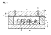
- FIG. 1 is a sectional view of a solar cell according to an embodiment of the present invention.
- the solar cell includes a first substrate 10 with a first electrode 11 and a porous film 30 including an adsorbed dye 40, a second substrate 20 facing the first substrate 10 with a predetermined distance therebetween and having a second electrode 21, and an electrolyte 50 disposed between the first and second substrates 10 and 20.
- the dye-adsorbed porous film 30 has a role of generating electrons upon receipt of the light incident thereto and delivering the electrons to the first electrode 11.
- the porous film 30 and the adsorbed dye 40 may be collectively referred to as a light absorption layer.
- the first substrate 10 having the first electrode 11 and the light absorption layer may be collectively referred to as the substrate/electrode/light absorption layer assembly.
- a separate case (not shown) may be provided external to the first and second substrates 10 and 20.
- the first substrate 10 which functions as a support for the first electrode 11, is formed with a transparent material that allows light to pass therethrough.
- the first substrate 10 may be formed with glass or plastic.
- the plastic may be selected from polyethylene terephthalate (PET), polyethylene naphthalate (PEN), polycarbonate (PC), polypropylene (PP), polyimide (PI), and triacetyl cellulose (TAC).
- PET polyethylene terephthalate
- PEN polyethylene naphthalate
- PC polycarbonate
- PP polypropylene
- PI polyimide
- TAC triacetyl cellulose
- the first substrate 10 is not limited to these materials, and other materials are possible.
- the first electrode 11 provided on the first substrate 10 may be formed with indium tin oxide (ITO), fluorine tin oxide (FTO), antimony tin oxide (ATO), zinc oxide (ZO), tin oxide (TO), ZnO-Ga 2 O 3 , or ZnO-Al 2 O 3 .
- ITO indium tin oxide
- FTO fluorine tin oxide
- ATO antimony tin oxide
- ZO zinc oxide
- tin oxide (TO) ZnO-Ga 2 O 3
- ZnO-Al 2 O 3 ZnO-Al 2 O 3
- the first electrode 11 is not limited to these materials, and other materials are possible.
- the first electrode 11 may be formed with a transparent material-based single layer structure, or a laminated layer structure.
- a contact area region 16 is formed between the first electrode 11 and the porous film 30.
- the contact area region 16 is for example made by forming prominent and depressed portions at the first electrode 11. More specifically, prominent and depressed portions are formed at a surface of the first substrate 10, and the first electrode 11 is formed on that rugged surface of the first substrate 10.
- the first electrode 11 conforms to the surface of the first substrate 10 such that the surface of the first electrode 11 also has the prominent and depressed portions, i. e. has a specific surface texture.
- Texture is the combination of fairly short wavelength deviations of a surface from the nominal surface. Texture includes roughness, waviness, and lay, that is, all of the deviations that are shorter in wavelength than form error deviations.
- Roughness includes the finest (shortest wavelength) irregularities of a surface. Roughness generally results from a particular production process or material condition. Waviness includes the more widely spaced (longer wavelength) deviations of a surface from its nominal shape.
- Waviness refers to the irregularities which are outside the roughness width cut off values and may be the result of workpiece or tool deflection during machining, vibrations or tool runout.
- Lay refers to the predominant direction of the surface texture. Ordinarily lay is determined by the particular production method and geometry used. Turning, milling, drilling, grinding, and other cutting tool machining processes usually produce a surface that has lay: striations or peaks and valleys in the direction that the tool was drawn across the surface. The shape of the lay can take one of several forms as shown below. Other processes produce surfaces with no characteristic direction: sand casting, peening, and grit blasting. Sometimes these surfaces are said to have a nondirectional, particulate, or protuberant lay.
- the root mean square (Rms) of the surface roughness of the surface of the first substrate 10 is in the range of 10nm to 3000nm, preferably in the range of 50 to 1500nm, most preferred in the range of 150 to 400nm. Since the first electrode 11 conforms to the surface of the first substrate 10, the Rms of the surface roughness at the surface of the first electrode 11 with the porous film 30 may also be in the range of 10nm to 3000nm. Typically, but not necessarily, the surface roughness of the first substrate 10 may be determined before the first electrode is deposited thereon, or in the absence of the first electrode and the surface roughness of the first electrode may be measured before the light absorption layer is formed thereon, or in the absence of the light absorption layer. The methods of determining the roughness of the surfaces are common knowledge and inter alia include optical and mechanical procedures. However, the surface roughness may also be determined under other methods or conditions.
- the lay of the surface texture may be formed in the shape of steps, meshes, scratches, scars, beds or other shapes.
- the porous film 30 is placed or formed on the first electrode 11.
- the porous film 30 includes metallic oxide particles 31 having a nanometer-level mean particle diameter.
- the metallic oxide particles 31 may comprise titanium oxide, zinc oxide, tin oxide, strontium oxide, indium oxide, iridium oxide, lanthanum oxide, vanadium oxide, molybdenum oxide, tungsten oxide, niobium oxide, magnesium oxide, aluminium oxide, yttrium oxide, scandium oxide, samarium oxide, gallium oxide, or strontium titanium oxide.
- the metallic oxide particles 31 of the porous film 30 may comprise titanium oxide TiO 2 .
- the metallic oxide particles 31 are not limited to these materials, and other materials are possible.
- the metallic oxide particles 31 with a nanometer-level mean particle diameter may be uniformly distributed with suitable porosity and surface roughness to form the porous film 30.
- a polymer (not shown), conductive micro particles (not shown), and light-scattering particles (not shown) may be added to the porous film 30.
- the polymer may be added to the porous film 30 to increase the porosity, diffusivity, and viscosity of the porous film 30, thereby enhancing the film formation and adhesion thereof.
- the polymer may be selected from polyethylene glycol (PEG), polyethylene oxide (PEO), polyvinyl alcohol (PVA), and polyvinyl pyrrolidone (PVP).
- PEG polyethylene glycol
- PEO polyethylene oxide
- PVA polyvinyl alcohol
- PVP polyvinyl pyrrolidone
- the polymer is not limited to these materials, and other materials are possible.
- the molecular weight of the polymer may be selected taking into account the method and conditions of formation of the porous film 30.
- Light-scattering particles may be added to the porous film 30 to extend the optical path within the solar cell to enhance the photoelectric conversion efficiency thereof.
- the light-scattering particles may be formed with the same material as the metallic oxide particles 31 for the porous film 30.
- the light scattering particles are not limited to these materials, and other materials are possible.
- the light-scattering particles preferably have a mean particle diameter of 100nm or more to effectively scatter the light.
- the second substrate 20 may be formed with glass or plastic.
- the plastic may be selected from polyethylene terephthalate, polyethylene naphthalate, polycarbonate, polypropylene, polyimide, and triacetyl cellulose.
- the second substrate 21 is not limited to these materials, and other materials are possible.
- the prominent and depressed portions functioning as the contact area region are not formed at the second electrode 21, and hence the Rms surface roughness of the first electrode 11 is greater than the Rms surface roughness of the second electrode 21.
- the Rms of the surface roughness of the second electrode 21 may be less than 10nm.
- the electrolyte 30 is not limited to a liquid electrolyte as described herein.
- the electrolyte 30 may be in other forms, such as a gel or solid electrolyte, provided that the electrolyte is present between the first and second electrodes 11 and 21.
- the contact area enlargement region 16 is formed by creating prominent and depressed portions at the first substrate 10.
- the first electrode 11, formed on the first substrate 10 conforms to the first substrate so that the contact area enlargement region 16 is formed at the first electrode 11.
- the surface of the first electrode 11 has the same prominent and depressed portions that were on the surface of the first substrate.
- prominent and depressed portions are formed at the first substrate 10 through mechanical treatment or chemical etching.
- the formation of for example prominent and depressed portions is not limited to these methods and other methods are possible.
- the mechanical treatment may be carried out by sandblasting or scratching, and the chemical etching may be performed by plasma etching or by dipping the substrate in hydrofluoric acid, nitric acid, hydrochloric acid, or mixed solutions thereof. Consequently, the Rms of the surface roughness of the first substrate 10 comes to be in the range of 10nm to 3000nm.
- the prominent and depressed portions defining the surface texture may be in the shape of steps, meshes, scratches, scars, beds or other shapes.
- a conductive layer is deposited onto a surface of the first substrate 10 with the prominent and depressed portions through sputtering, chemical vapor deposition (CVD), or spray pyrolysis deposition (SPD) to thereby form the first electrode 11.
- the formation of the first electrode 11 is not limited to these methods and other methods are possible. Because the first electrode 11 is relatively thin, the prominent and depressed portions that were formed at the first substrate 10 also appear at the surface of the first electrode 11. The resulting prominent and depressed portions of the first electrode 11 function as the contact area enlargement region 16. With the formation of the surface texture of the substrate 10 (especially the prominent and depressed portions), the Rms of the surface roughness of the first electrode 11 comes to be in the range of 10nm to 3000nm.
- the first electrode 11 may be formed with indium tin oxide, fluorine tin oxide, antimony tin oxide, zinc oxide, tin oxide, ZnO-Ga 2 O 3 , or ZnO-Al 2 O 3 or other conductive materials.
- the first electrode 11 may be formed with a single layer structure based on a transparent material, or with a laminated layer structure.
- a paste containing metallic oxide particles 31 is coated onto the first electrode 11 and heat-treated to thereby form a porous film 30.
- the paste may contain a polymer, light-scattering particles, and conductive micro particles in addition to the metallic oxide.
- the coating of the paste may be performed in various ways including with a doctor blade, by screen printing, by spin coating, by spraying, and by wet coating.
- the method of coating may be selected to be compatible with a particular paste that is used. Alternatively, if a particular method of coating has already been selected, the paste may be selected to be compatible with the chosen method of coating.
- the heat treatment o may be performed on the paste-coated electrode at 450 to 600°C for 30 minutes. On the other hand, if the paste does not contain a binder, the heat treatment may be performed at 200°C or less. However, different heating temperatures may be selected depending upon the composition of the paste, and heating temperature of the paste-coated electrode is not limited to the above examples.
- the first substrate 10 with the first electrode 11 and the porous film 30 formed thereon is dipped in a alcoholic solution containing a dissolved dye for a predetermined period of time, thereby adsorbing the dye 40 into the porous film 30, thereby creating the light absorption layer.
- the transparent electrode 21a and a catalyst electrode 21b are sequentially formed on the second substrate 20, which can be made of glass or plastic, for example, to thereby form a second electrode 21.
- the material for the second substrate 20 may be the same as that for the first substrate 10, and hence a detailed explanation thereof will be omitted.
- the material for the transparent electrode 21a may be the same as that for the first electrode 11, and a detailed explanation thereof will be omitted.
- the catalyst electrode 21b may be formed, for example, with platinum, ruthenium, rhodium, palladium, iridium, osmium, WO 3 , TiO 2 , or C.
- the formation of the catalyst electrode 21b may be accomplished, for example, through physical vapour deposition (such as electroplating, sputtering, and electron beam deposition), or wet coating (such as spin coating, dip coating, and flow coating).
- the adhesive 61 may be formed with a thermoplastic polymer film (such as, for example, a resin provided by DuPont under the registered trademark SURLYNTM), an epoxy resin, or an ultraviolet hardener.
- a thermoplastic polymer film such as, for example, a resin provided by DuPont under the registered trademark SURLYNTM
- an epoxy resin such as, for example, a resin provided by DuPont under the registered trademark SURLYNTM
- an ultraviolet hardener such as, for example, a resin provided by DuPont under the registered trademark SURLYNTM
- the thermoplastic polymer film is placed between the first and second substrates 10 and 20, which are then thermally pressed, thereby attaching the first and second substrates 10 and 20 to each other.
- An electrolyte 50 is injected into the interior between the first and second substrates 10 and 20 through holes 25a formed at the second substrate 20 and the second electrode 21, and the holes 25a are sealed using an adhesive 62 and a cover glass 63. (if a solid or other non-liquid form of electrolyte is used, the electrolyte is added before the first and second substrates 10 and 20 are joined.) In this way, a solar cell is completed.
- a separate case (not shown) may be provided external to the first and second substrates 10 and 20.
- FIG. 3 is a sectional view of a solar cell according to another embodiment of the present invention.
- like reference numerals are used for the same or similar structural components as those related to the previous embodiment, and only the different structures will now be explained.
- a method of manufacturing the solar cell is also substantially the same as that related to the previous embodiment, and hence a detailed explanation thereof will be omitted except for the formation of the first electrode.
- the first substrate 110 has a flat and smooth surface with no rugged portion. Prominent and depressed portions are formed at the first electrode 111 to create a contact area region 116.
- the first electrode 111 is formed through sputtering, chemical vapour deposition, or spray pyrolysis deposition, and the processing conditions are controlled such that the surface roughness of the first electrode 111 has an Rms of 10nm to 3000nm.
- a solar cell according to the present invention will be now specifically explained by way of examples.
- the examples are given only to illustrate the present invention, but not intended to limit the scope of the present invention.
- a first substrate was formed with soda-lime glass having a horizontal side of 2.2cm, a vertical side of 2.2cm, and a thickness of 1.1 mm.
- the first substrate was ultrasonically cleaned using distilled water.
- the clean first substrate was dipped in a hydrofluoric aqueous solution containing 49 wt% of hydrofluoric acid for 20 minutes, and etched.
- the first substrate was then ultrasonic-wave cleaned using distilled water, and an indium tin oxide layer with a thickness of 500nm was deposited onto the first substrate through spray pyrolysis deposition, thereby forming a first electrode.
- a paste containing TiO 2 particles with a mean particle diameter of 7nm-50nm was coated onto a surface of the first electrode with an area of 1cm 2 through screen printing, and heat-treated at 450°C for 30 minutes to thereby form a TiO 2 -contained porous film with a thickness of 15 ⁇ m.
- the first substrate with the porous film and the first electrode was dipped in a 0.3mM solution of ruthenium (4,4-dicarboxy-2,2'-bipyridine) 2 (NCS) 2 for 24 hours, thereby adsorbing the dye into the porous film.
- the dye-adsorbed porous film was cleaned using ethanol.
- a second substrate was formed with soda-lime glass having a horizontal side of 2.2cm, a vertical side of 2.2cm, and a thickness of 1.1 mm.
- the second substrate was ultrasonically cleaned using distilled water. Two holes were formed at the second substrate. Thereafter, an indium tin oxide layer with a thickness of 500nm was deposited onto the second substrate through spray pyrolysis deposition to form a transparent electrode.
- a catalyst electrode based on platinum with a surface resistivity of 3 ⁇ /sq was formed on the transparent electrode through sputtering.
- the first and second substrates were arranged such that the porous film formed on the first electrode faced the second electrode.
- a thermoplastic polymer film was disposed between the first and second substrates, and thermally pressed to thereby attach the first and second substrates to each other.
- An electrolyte was injected into the interior between the first and second substrates through the two holes formed at the second substrate and the second electrode, and the holes were sealed using a thermoplastic polymer film and a cover glass, thereby completing a solar cell.
- the electrolyte was based on a solution wherein 21.928g of tetrapropylammonium iodide and 1.931g of iodine (I 2 ) were dissolved in 100ml of a mixed solvent of 80 vol% of ethylene carbonate and 20 vol% of acetonitrile.
- a solar cell was manufactured in the same way as in Example 1 except that the first substrate was etched for 40 minutes.
- a solar cell was manufactured in the same way as in Example 1 except that the first substrate was etched for 90 minutes.
- a solar cell was manufactured in the same way as in Example 1 except that the first substrate was etched for 300 minutes.
- a solar cell was manufactured in the same way as in Example 1 except that the first substrate was etched for 600 minutes.
- a solar cell was manufactured in the same way as in Example 1 except that the first substrate was not etched.
- a solar cell was manufactured in the same way as in Example 1 except that the first substrate was etched for 1200 minutes.
- FIG. 2 An exemplary atomic force microscope (AFM) image of the surface of the first electrode is presented in FIG. 2. It can be predicted that the contact area between the first electrode and the porous film would be increased due to the surface texture having prominent and depressed portions. Only an image of the surface of the first electrode of the solar cell according to Example 2 is shown in FIG. 2, but the same type of result may be expected with the other examples.
- AFM atomic force microscope
- the Rms of the surface roughness, open circuit voltage, short circuit current, fill factor, light transmittance, and efficiency are listed in Table 1.
- the open circuit voltage was evaluated from the voltage-current curve where a light source of 100mW/cm 2 was corrected by a Si standard cell, and measured.
- the listing sequence is made in accordance with the dimensions of the Rms of the surface roughness.
- Table 1 Rms of surface roughness (nm) Open circuit voltage (V) Short circuit current (mA) Fill factor Light transmittance (%) Efficiency (%) Com.
- the solar cells according to Examples 1 to 6 have very high short circuit currents with fill factors similar to each other, compared to the solar cells according to Comparative Examples 1 and 2.
- the short circuit currents of the solar cells according to Examples 1 to 6, especially according to Examples 2 to 6, were higher than those of the solar cells according to Comparative Examples 1 and 2, and this was presumed to be due to the increase in contact area between the porous film and the first electrode. It turned out that the solar cells according to Examples 1 to 6, especially according to Examples 3 and 4, had excellent efficiency due to the high short circuit current thereof, compared to the solar cells according to Comparative Examples 1 and 2.
- the Rms of the surface roughness should be in the range of 10 to 3000nm, preferably in the range of 50 to 1500 nm (with respect to the short circuit current of Examples 2 to 6), most preferred in the range of 150 to 400nm (with respect to the efficiency of Examples 3 and 4).
- the light transmittance deteriorated.
- the decrease in efficiency due to the deterioration in light transmittance was greater than the increase in efficiency due to the enhancement in short circuit current based upon the increased contact area, and hence, the overall efficiency was lower.
- a contact area enlargement region is formed at the first electrode at the interface with the light absorption layer, thereby increasing and enhancing the contact characteristics of the light absorption layer and the first electrode and increasing the contact area therebetween. Accordingly, the mobility and migration speed of the excited electrons are improved so that the short circuit current intensity is increased, and the photoelectric conversion efficiency of the solar cell is enhanced.
- a dye-sensitized solar cell is exemplified as a solar cell.
- the inventive structure may be applied to other types of solar cells. That is, other types of solar cells having an electrode and a light absorption layer may have an increased contact area between the electrode and the light absorption layer.
Landscapes
- Engineering & Computer Science (AREA)
- Power Engineering (AREA)
- Microelectronics & Electronic Packaging (AREA)
- Photovoltaic Devices (AREA)
- Hybrid Cells (AREA)
Abstract
Description
- Aspects of the present invention relate to a solar cell and a manufacturing method thereof, and in particular, to a solar cell with high energy efficiency, and a method of manufacturing the solar cell.
- Generally, a solar cell generates electrical energy using solar energy, an unlimited energy source, in an environmentally friendly way. Typical solar cells include silicon solar cells, dye-sensitized solar cells, etc.
- A solar cell typically has a first electrode having a dye-adsorbed porous film formed thereon, and a second electrode facing the first electrode with a predetermined distance therebetween. The dye-sensitized solar cell is produced with simplified processing steps and a lower production cost compared to the silicon solar cell. Furthermore, since the first and second electrodes in the dye-sensitized solar cell are formed with a transparent material, the dye-sensitized solar cell may be used in constructing an outer wall for buildings or greenhouses.
- However, the dye-sensitized solar cell has a lower photoelectric conversion efficiency than the silicon solar cell, and it is limited in the practical usage thereof. In order to increase the photoelectric conversion efficiency, it has been proposed that the reflectivity of the second electrode should be increased or that light-scattering particles should be used, but the proposed methods are limited in the extent to which they can increase the photoelectric conversion efficiency of the dye-sensitized solar cell. In this regard, it is desirable to develop a new technology for enhancing the photoelectric conversion efficiency of the dye-sensitized solar cell as well as of other kinds of solar cells.
- Aspects of the present invention provide a solar cell with enhanced photoelectric conversion efficiency, and a method of manufacturing the solar cell.
- According to a first aspect of the invention there is provided a solar cell comprising a substrate, an electrode formed on the substrate and a light absorption layer formed on the electrode. The solar cell is characterized in that a contact enlargement region which is formed between the electrode and the light absorption layer.
- Preferably, a root mean square surface roughness of the electrode in the contact enlargement region between the electrode and the light absorption layer is in the range of 10 nm to 3000 nm, preferably in the range of 50 nm to 1500 nm, most preferred in the range of 150 nm to 400 nm.
- A lay of the contact area enlargement region may include the shapes of steps, meshes, scratches, scars or beds. A root mean square surface roughness of the substrate may be in the range of 10 nm to 3000 nm.
- The solar cell may further comprise a second substrate, wherein the first and second substrates facing each other. A second electrode is formed on the second substrate, wherein the root mean square surface roughness of the first electrode is greater than a root mean square surface roughness of the second electrode.
- According to a second aspect of the invention there is provided a method of manufacturing a solar cell. The method comprises the steps of:
- providing a substrate;
- forming an electrode on a surface of the substrate and controlling processing conditions of the forming such that a contact enlargement region, which is designated for bearing a light absorption layer, is formed on the electrode; and
- forming the light absorption layer on the electrode.
- Preferably, a root mean square of the roughness of the surface of the electrode in the contact enlargement region is in the range of 10 nm to 3000 nm.
- The step of providing a substrate may include the controlling of processing conditions of a forming of the substrate such that a root mean square of roughness of a surface of the substrate is in the range of 10 nm to 3000 nm in a region which is designated for bearing the electrode.
- The root mean square roughness of the substrate may be controlled through mechanical or chemical treatment. The mechanical or chemical treatment may include any of sandblasting, scratching, or plasma etching. The chemical treatment may include etching performed with a solution selected from the group consisting of nitric acid, hydrochloric acid, hydrofluoric acid, and mixtures thereof.
- These and/or other aspects and advantages of the invention will become apparent and more readily appreciated from the following description of the embodiments, taken in conjunction with the accompanying drawings of which:
- FIG. 1 is a sectional view of a solar cell according to an embodiment of the present invention;
- FIG. 2 is an atomic force microscope (AFM) image of a surface of a first electrode for a solar cell according to the embodiment of FIG. 1, wherein the electrode has prominent and depressed portions according to ; and
- FIG. 3 is a sectional view of a solar cell according to another embodiment of the present invention.
- Reference will now be made in detail to the present embodiments of the present invention, examples of which are illustrated in the accompanying drawings, wherein like reference numerals refer to the like elements throughout. The embodiments are described below in order to explain the present invention by referring to the figures.
- FIG. 1 is a sectional view of a solar cell according to an embodiment of the present invention.
- As shown in FIG. 1, the solar cell according to aspects of the present embodiment includes a
first substrate 10 with afirst electrode 11 and aporous film 30 including anadsorbed dye 40, asecond substrate 20 facing thefirst substrate 10 with a predetermined distance therebetween and having asecond electrode 21, and anelectrolyte 50 disposed between the first andsecond substrates porous film 30 has a role of generating electrons upon receipt of the light incident thereto and delivering the electrons to thefirst electrode 11. Theporous film 30 and theadsorbed dye 40 may be collectively referred to as a light absorption layer. Thefirst substrate 10 having thefirst electrode 11 and the light absorption layer may be collectively referred to as the substrate/electrode/light absorption layer assembly. A separate case (not shown) may be provided external to the first andsecond substrates - In this embodiment, the
first substrate 10, which functions as a support for thefirst electrode 11, is formed with a transparent material that allows light to pass therethrough. Thefirst substrate 10 may be formed with glass or plastic. The plastic may be selected from polyethylene terephthalate (PET), polyethylene naphthalate (PEN), polycarbonate (PC), polypropylene (PP), polyimide (PI), and triacetyl cellulose (TAC). Thefirst substrate 10 is not limited to these materials, and other materials are possible. - The
first electrode 11 provided on thefirst substrate 10 may be formed with indium tin oxide (ITO), fluorine tin oxide (FTO), antimony tin oxide (ATO), zinc oxide (ZO), tin oxide (TO), ZnO-Ga2O3, or ZnO-Al2O3. Thefirst electrode 11 is not limited to these materials, and other materials are possible. Thefirst electrode 11 may be formed with a transparent material-based single layer structure, or a laminated layer structure. - In this embodiment, a
contact area region 16 is formed between thefirst electrode 11 and theporous film 30. Thecontact area region 16 is for example made by forming prominent and depressed portions at thefirst electrode 11. More specifically, prominent and depressed portions are formed at a surface of thefirst substrate 10, and thefirst electrode 11 is formed on that rugged surface of thefirst substrate 10. Thefirst electrode 11 conforms to the surface of thefirst substrate 10 such that the surface of thefirst electrode 11 also has the prominent and depressed portions, i. e. has a specific surface texture. - Surface texture is the combination of fairly short wavelength deviations of a surface from the nominal surface. Texture includes roughness, waviness, and lay, that is, all of the deviations that are shorter in wavelength than form error deviations.
- Roughness includes the finest (shortest wavelength) irregularities of a surface. Roughness generally results from a particular production process or material condition. Waviness includes the more widely spaced (longer wavelength) deviations of a surface from its nominal shape.
- Waviness refers to the irregularities which are outside the roughness width cut off values and may be the result of workpiece or tool deflection during machining, vibrations or tool runout.
- Lay refers to the predominant direction of the surface texture. Ordinarily lay is determined by the particular production method and geometry used. Turning, milling, drilling, grinding, and other cutting tool machining processes usually produce a surface that has lay: striations or peaks and valleys in the direction that the tool was drawn across the surface. The shape of the lay can take one of several forms as shown below. Other processes produce surfaces with no characteristic direction: sand casting, peening, and grit blasting. Sometimes these surfaces are said to have a nondirectional, particulate, or protuberant lay.
- The root mean square (Rms) of the surface roughness of the surface of the
first substrate 10 is in the range of 10nm to 3000nm, preferably in the range of 50 to 1500nm, most preferred in the range of 150 to 400nm. Since thefirst electrode 11 conforms to the surface of thefirst substrate 10, the Rms of the surface roughness at the surface of thefirst electrode 11 with theporous film 30 may also be in the range of 10nm to 3000nm. Typically, but not necessarily, the surface roughness of thefirst substrate 10 may be determined before the first electrode is deposited thereon, or in the absence of the first electrode and the surface roughness of the first electrode may be measured before the light absorption layer is formed thereon, or in the absence of the light absorption layer. The methods of determining the roughness of the surfaces are common knowledge and inter alia include optical and mechanical procedures. However, the surface roughness may also be determined under other methods or conditions. - It is difficult in practice to form prominent and depressed portions to provide an Rms of the surface roughness of less than 10nm. On the other hand, when the Rms of the surface roughness exceeds 3000nm, light transmittance is lowered and the energy efficiency deteriorates to such an extent as to offset the efficiency enhancement gained by the increase in the contact area. Furthermore, if the Rms of the surface roughness does not exceed 3000nm, the electron transfer may be performed more effectively. In addition, it has been shown that a Rms of the surface roughness of the
electrode 11 in the range of 50 to 1500nm results in an outstanding range of short circuit current of the solar cell and a Rms of the surface roughness of theelectrode 11 in the range of 150 to 400nm in addition leads to a solar cell having an extraordinary efficiency (see especially experimental part, table 1). - Increasing the Rms of the surface roughness of the
electrode 11 enlarges the contact area between thefirst electrode 11 and theporous film 30. The lay of the surface texture may be formed in the shape of steps, meshes, scratches, scars, beds or other shapes. - The
porous film 30 is placed or formed on thefirst electrode 11. Theporous film 30 includesmetallic oxide particles 31 having a nanometer-level mean particle diameter. Themetallic oxide particles 31 may comprise titanium oxide, zinc oxide, tin oxide, strontium oxide, indium oxide, iridium oxide, lanthanum oxide, vanadium oxide, molybdenum oxide, tungsten oxide, niobium oxide, magnesium oxide, aluminium oxide, yttrium oxide, scandium oxide, samarium oxide, gallium oxide, or strontium titanium oxide. For instance, themetallic oxide particles 31 of theporous film 30 may comprise titanium oxide TiO2. Themetallic oxide particles 31 are not limited to these materials, and other materials are possible. - As a non-limiting example, the
metallic oxide particles 31 with a nanometer-level mean particle diameter may be uniformly distributed with suitable porosity and surface roughness to form theporous film 30. - In order to enhance the performance characteristics of the
porous film 30, a polymer (not shown), conductive micro particles (not shown), and light-scattering particles (not shown) may be added to theporous film 30. - The polymer may be added to the
porous film 30 to increase the porosity, diffusivity, and viscosity of theporous film 30, thereby enhancing the film formation and adhesion thereof. The polymer may be selected from polyethylene glycol (PEG), polyethylene oxide (PEO), polyvinyl alcohol (PVA), and polyvinyl pyrrolidone (PVP). The polymer is not limited to these materials, and other materials are possible. The molecular weight of the polymer may be selected taking into account the method and conditions of formation of theporous film 30. - Conductive micro particles may be added to the
porous film 30 to enhance the mobility of the excited electrons. For instance, the conductive micro particles may comprise indium tin oxide. The conductive micro particles are not limited to these materials, and other materials are possible. - Light-scattering particles may be added to the
porous film 30 to extend the optical path within the solar cell to enhance the photoelectric conversion efficiency thereof. The light-scattering particles may be formed with the same material as themetallic oxide particles 31 for theporous film 30. The light scattering particles are not limited to these materials, and other materials are possible. The light-scattering particles preferably have a mean particle diameter of 100nm or more to effectively scatter the light. - The
dye 40 is adsorbed onto the surface of themetallic oxide particles 31 of theporous film 30 to absorb external light and excite electrons. Thedye 40 may be formed with a metal complex containing aluminium (AI), platinum (Pt), palladium (Pd), europium (Eu), lead (Pb), or iridium (Ir), or with a ruthenium (Ru) complex. Ruthenium belongs to the platinum group, and a ruthenium-containing dye is commonly used as an organic metal complex compound. The metal complex is not limited to these materials, and other materials are possible. - Furthermore, a dye may be selected that is capable of improving the absorption of long wavelength visible rays to enhance the photoelectric conversion efficiency and/or that is capable of easily emitting electrons. For example, an organic dye may be used. The organic dye may be used independently or in association with a metal complex such as, for example, the ruthenium complex mentioned above. The organic dye may be selected from coumarin, porphyrin, xanthene, riboflavin, and triphenylmethane. The organic dye is not limited to these materials, and other materials are possible.
- The
second substrate 20, which faces thefirst substrate 10 in the assembled solar cell, supports thesecond electrode 21, and is formed with a transparent material. Thesecond substrate 20 may be formed with glass or plastic. The plastic may be selected from polyethylene terephthalate, polyethylene naphthalate, polycarbonate, polypropylene, polyimide, and triacetyl cellulose. Thesecond substrate 21 is not limited to these materials, and other materials are possible. - The
second electrode 21 formed on thesecond substrate 20 faces thefirst electrode 11 and includes atransparent electrode 21a and acatalyst electrode 21b. - The
transparent electrode 21a may be formed with a transparent material such as indium tin oxide, fluorine tin oxide, antimony tin oxide, zinc oxide, tin oxide, ZnO-Ga2O3, and ZnO-Al2O3. Thetransparent electrode 21a is not limited to these materials, and other materials are possible. Thetransparent electrode 21a may be formed with a single layer structure based on a transparent material, or with a laminated layer structure. Thecatalyst electrode 21b activates the redox couple, and may be formed with platinum, ruthenium, palladium, iridium, rhodium, osmium, carbon, WO3, or TiO2. Thecatalyst electrode 21b is not limited to these materials, and other materials are possible. - In this embodiment, the prominent and depressed portions functioning as the contact area region are not formed at the
second electrode 21, and hence the Rms surface roughness of thefirst electrode 11 is greater than the Rms surface roughness of thesecond electrode 21. The Rms of the surface roughness of thesecond electrode 21 may be less than 10nm. - The first and
second substrates electrolyte 50 is injected into the interior between the first andsecond electrodes holes 25a formed at thesecond substrate 20 and thesecond electrode 21. Theelectrolyte 50 is uniformly diffused into theporous film 30. Theelectrolyte 50 may comprise a solution including iodide and triiodide. The electrolyte receives and transfers electrons from thesecond electrode 21 to thedye 40 through reduction and oxidation. Theholes 25a formed at thesecond substrate 20 and thesecond electrode 21 are sealed by an adhesive 62 and acover glass 63. - The
electrolyte 30 is not limited to a liquid electrolyte as described herein. For example, theelectrolyte 30 may be in other forms, such as a gel or solid electrolyte, provided that the electrolyte is present between the first andsecond electrodes - When external light such as sunlight hits the interior of the solar cell, photons are absorbed into the dye so that the dye is shifted from an inactive state to an excited state to thereby generate electron-hole pairs. The excited electrons migrate into the conduction bands of the
metallic oxide particles 31 for theporous film 30, and flow to an external circuit (not shown) through thefirst electrode 11, and are then transferred to thesecond electrode 21. Meanwhile, as the iodide within theelectrolyte 50 is oxidized into triiodide, the oxidized dye is reduced, and the triiodide is reacts with the electrons that have reached thesecond electrode 21 to be thereby reduced into iodide. The solar cell operates due to the migration of electrons. - Unlike the silicon solar cell, the dye-sensitized solar cell operates through a reaction at an interface, in particular, the interface between the
porous film 30 of the light absorption layer and theelectrode 11. Hence, it is beneficial to improve the characteristics of this interface. In this embodiment, a contactarea enlargement region 16 is formed at thefirst substrate 10 and thefirst electrode 11 with prominent and depressed portions to thereby improve the contact characteristic thereof. The contact characteristic of thefirst electrode 11 and theporous film 30 is improved and the contact area therebetween is increased, thereby enhancing the mobility and speed of the electrons. - In this embodiment, the contact
area enlargement region 16 is formed by creating prominent and depressed portions at thefirst substrate 10. Thefirst electrode 11, formed on thefirst substrate 10 conforms to the first substrate so that the contactarea enlargement region 16 is formed at thefirst electrode 11. In other words, the surface of thefirst electrode 11 has the same prominent and depressed portions that were on the surface of the first substrate. When the prominent and depressed portions are formed at thefirst substrate 10, processing is easily carried out, and thefirst electrode 11 is protected from possible processing failure, compared to the case in which the prominent and depressed portions are formed only at thefirst electrode 11 and not at thefirst substrate 10. When the prominent and depressed portions are directly formed at thefirst electrode 11 through etching, thefirst electrode 11 may suffer unwanted damage. - A method of manufacturing the above-structured solar cell will be now explained in detail.
- A
first substrate 10 made of a transparent material such as glass or plastic is provided. The plastic may be selected from polyethylene terephthalate, polyethylene naphthalate, polycarbonate, polypropylene, polyimide, and triacetyl cellulose. As noted above, thefirst substrate 10 is not limited to these materials, and other materials are possible. - Thereafter, prominent and depressed portions are formed at the
first substrate 10 through mechanical treatment or chemical etching. The formation of for example prominent and depressed portions is not limited to these methods and other methods are possible. The mechanical treatment may be carried out by sandblasting or scratching, and the chemical etching may be performed by plasma etching or by dipping the substrate in hydrofluoric acid, nitric acid, hydrochloric acid, or mixed solutions thereof. Consequently, the Rms of the surface roughness of thefirst substrate 10 comes to be in the range of 10nm to 3000nm. The prominent and depressed portions defining the surface texture may be in the shape of steps, meshes, scratches, scars, beds or other shapes. - A conductive layer is deposited onto a surface of the
first substrate 10 with the prominent and depressed portions through sputtering, chemical vapor deposition (CVD), or spray pyrolysis deposition (SPD) to thereby form thefirst electrode 11. The formation of thefirst electrode 11 is not limited to these methods and other methods are possible. Because thefirst electrode 11 is relatively thin, the prominent and depressed portions that were formed at thefirst substrate 10 also appear at the surface of thefirst electrode 11. The resulting prominent and depressed portions of thefirst electrode 11 function as the contactarea enlargement region 16. With the formation of the surface texture of the substrate 10 (especially the prominent and depressed portions), the Rms of the surface roughness of thefirst electrode 11 comes to be in the range of 10nm to 3000nm. As stated above, thefirst electrode 11 may be formed with indium tin oxide, fluorine tin oxide, antimony tin oxide, zinc oxide, tin oxide, ZnO-Ga2O3, or ZnO-Al2O3 or other conductive materials. Thefirst electrode 11 may be formed with a single layer structure based on a transparent material, or with a laminated layer structure. - A paste containing
metallic oxide particles 31 is coated onto thefirst electrode 11 and heat-treated to thereby form aporous film 30. The paste may contain a polymer, light-scattering particles, and conductive micro particles in addition to the metallic oxide. - The coating of the paste may be performed in various ways including with a doctor blade, by screen printing, by spin coating, by spraying, and by wet coating. The method of coating may be selected to be compatible with a particular paste that is used. Alternatively, if a particular method of coating has already been selected, the paste may be selected to be compatible with the chosen method of coating.
- If the paste contains a binder, the heat treatment o may be performed on the paste-coated electrode at 450 to 600°C for 30 minutes. On the other hand, if the paste does not contain a binder, the heat treatment may be performed at 200°C or less. However, different heating temperatures may be selected depending upon the composition of the paste, and heating temperature of the paste-coated electrode is not limited to the above examples.
- Thereafter, the
first substrate 10 with thefirst electrode 11 and theporous film 30 formed thereon is dipped in a alcoholic solution containing a dissolved dye for a predetermined period of time, thereby adsorbing thedye 40 into theporous film 30, thereby creating the light absorption layer. - The
transparent electrode 21a and acatalyst electrode 21b are sequentially formed on thesecond substrate 20, which can be made of glass or plastic, for example, to thereby form asecond electrode 21. The material for thesecond substrate 20 may be the same as that for thefirst substrate 10, and hence a detailed explanation thereof will be omitted. Similarly, the material for thetransparent electrode 21a may be the same as that for thefirst electrode 11, and a detailed explanation thereof will be omitted. - The
catalyst electrode 21b may be formed, for example, with platinum, ruthenium, rhodium, palladium, iridium, osmium, WO3, TiO2, or C. The formation of thecatalyst electrode 21b may be accomplished, for example, through physical vapour deposition (such as electroplating, sputtering, and electron beam deposition), or wet coating (such as spin coating, dip coating, and flow coating). For example, when thecatalyst electrode 21b is formed with platinum, H2PtCl6 may be dissolved in an organic solvent such as methanol, ethanol, and isopropyl alcohol (IPA) to make a solution, and the solution may be wet-coated onto thetransparent electrode 21a and heat-treated at 400°C under an air or oxygen atmosphere. - Thereafter, the first and
second substrates first electrode 11 and theporous film 30 face thesecond electrode 21, and are attached to each other using an adhesive 61. The adhesive 61 may be formed with a thermoplastic polymer film (such as, for example, a resin provided by DuPont under the registered trademark SURLYN™), an epoxy resin, or an ultraviolet hardener. When the adhesive 61 is formed with a thermoplastic polymer film, the thermoplastic polymer film is placed between the first andsecond substrates second substrates - An
electrolyte 50 is injected into the interior between the first andsecond substrates holes 25a formed at thesecond substrate 20 and thesecond electrode 21, and theholes 25a are sealed using an adhesive 62 and acover glass 63. (if a solid or other non-liquid form of electrolyte is used, the electrolyte is added before the first andsecond substrates second substrates - FIG. 3 is a sectional view of a solar cell according to another embodiment of the present invention. In this embodiment, like reference numerals are used for the same or similar structural components as those related to the previous embodiment, and only the different structures will now be explained. A method of manufacturing the solar cell is also substantially the same as that related to the previous embodiment, and hence a detailed explanation thereof will be omitted except for the formation of the first electrode.
- In this embodiment, the
first substrate 110 has a flat and smooth surface with no rugged portion. Prominent and depressed portions are formed at thefirst electrode 111 to create acontact area region 116. Thefirst electrode 111 is formed through sputtering, chemical vapour deposition, or spray pyrolysis deposition, and the processing conditions are controlled such that the surface roughness of thefirst electrode 111 has an Rms of 10nm to 3000nm. - A solar cell according to the present invention will be now specifically explained by way of examples. The examples are given only to illustrate the present invention, but not intended to limit the scope of the present invention.
- A first substrate was formed with soda-lime glass having a horizontal side of 2.2cm, a vertical side of 2.2cm, and a thickness of 1.1 mm. The first substrate was ultrasonically cleaned using distilled water. The clean first substrate was dipped in a hydrofluoric aqueous solution containing 49 wt% of hydrofluoric acid for 20 minutes, and etched. The first substrate was then ultrasonic-wave cleaned using distilled water, and an indium tin oxide layer with a thickness of 500nm was deposited onto the first substrate through spray pyrolysis deposition, thereby forming a first electrode.
- A paste containing TiO2 particles with a mean particle diameter of 7nm-50nm was coated onto a surface of the first electrode with an area of 1cm2 through screen printing, and heat-treated at 450°C for 30 minutes to thereby form a TiO2-contained porous film with a thickness of 15µm.
- The first substrate with the porous film and the first electrode was dipped in a 0.3mM solution of ruthenium (4,4-dicarboxy-2,2'-bipyridine)2(NCS)2 for 24 hours, thereby adsorbing the dye into the porous film. The dye-adsorbed porous film was cleaned using ethanol.
- A second substrate was formed with soda-lime glass having a horizontal side of 2.2cm, a vertical side of 2.2cm, and a thickness of 1.1 mm. The second substrate was ultrasonically cleaned using distilled water. Two holes were formed at the second substrate. Thereafter, an indium tin oxide layer with a thickness of 500nm was deposited onto the second substrate through spray pyrolysis deposition to form a transparent electrode. A catalyst electrode based on platinum with a surface resistivity of 3 Ω/sq was formed on the transparent electrode through sputtering.
- The first and second substrates were arranged such that the porous film formed on the first electrode faced the second electrode. A thermoplastic polymer film was disposed between the first and second substrates, and thermally pressed to thereby attach the first and second substrates to each other. An electrolyte was injected into the interior between the first and second substrates through the two holes formed at the second substrate and the second electrode, and the holes were sealed using a thermoplastic polymer film and a cover glass, thereby completing a solar cell. The electrolyte was based on a solution wherein 21.928g of tetrapropylammonium iodide and 1.931g of iodine (I2) were dissolved in 100ml of a mixed solvent of 80 vol% of ethylene carbonate and 20 vol% of acetonitrile.
- A solar cell was manufactured in the same way as in Example 1 except that the first substrate was etched for 40 minutes.
- A solar cell was manufactured in the same way as in Example 1 except that the first substrate was etched for 90 minutes.
- A solar cell was manufactured in the same way as in Example 1 except that the first substrate was etched for 150 minutes.
- A solar cell was manufactured in the same way as in Example 1 except that the first substrate was etched for 300 minutes.
- A solar cell was manufactured in the same way as in Example 1 except that the first substrate was etched for 600 minutes.
- A solar cell was manufactured in the same way as in Example 1 except that the first substrate was not etched.
- A solar cell was manufactured in the same way as in Example 1 except that the first substrate was etched for 1200 minutes.
- With the solar cell according to the Example 2, an exemplary atomic force microscope (AFM) image of the surface of the first electrode is presented in FIG. 2. It can be predicted that the contact area between the first electrode and the porous film would be increased due to the surface texture having prominent and depressed portions. Only an image of the surface of the first electrode of the solar cell according to Example 2 is shown in FIG. 2, but the same type of result may be expected with the other examples.
- For the solar cells according to Examples 1 to 6 and Comparative Examples 1 and 2, the Rms of the surface roughness, open circuit voltage, short circuit current, fill factor, light transmittance, and efficiency are listed in Table 1. The open circuit voltage was evaluated from the voltage-current curve where a light source of 100mW/cm2 was corrected by a Si standard cell, and measured. For clearer understanding, the listing sequence is made in accordance with the dimensions of the Rms of the surface roughness.
Table 1 Rms of surface roughness (nm) Open circuit voltage (V) Short circuit current (mA) Fill factor Light transmittance (%) Efficiency (%) Com. Ex. 1 8 0.763 6.810 0.613 82.2 3.187 Ex.1 38 0.751 7.090 0.611 82.1 3.253 Ex.2 70 0.713 8.185 0.600 81.4 3.499 Ex.3 180 0.724 8.214 0.595 81.3 3.538 Ex.4 325 0.691 8.199 0.641 80.5 3.632 Ex.5 680 0.678 8.105 0.613 80.1 3.370 Ex.6 1280 0.671 8.091 0.591 79.1 3.209 Com. Ex.2 3200 0.614 7.610 0.577 76.5 2.700 - It is known from Table 1 that the solar cells according to Examples 1 to 6 have very high short circuit currents with fill factors similar to each other, compared to the solar cells according to Comparative Examples 1 and 2. The short circuit currents of the solar cells according to Examples 1 to 6, especially according to Examples 2 to 6, were higher than those of the solar cells according to Comparative Examples 1 and 2, and this was presumed to be due to the increase in contact area between the porous film and the first electrode. It turned out that the solar cells according to Examples 1 to 6, especially according to Examples 3 and 4, had excellent efficiency due to the high short circuit current thereof, compared to the solar cells according to Comparative Examples 1 and 2. Hence, it is shown that the Rms of the surface roughness should be in the range of 10 to 3000nm, preferably in the range of 50 to 1500 nm (with respect to the short circuit current of Examples 2 to 6), most preferred in the range of 150 to 400nm (with respect to the efficiency of Examples 3 and 4).
- As the Rms of the surface roughness increased, the light transmittance deteriorated. At an Rms of the surface roughness of 3200, according to the solar cell of Comparative Example 2, the decrease in efficiency due to the deterioration in light transmittance was greater than the increase in efficiency due to the enhancement in short circuit current based upon the increased contact area, and hence, the overall efficiency was lower.
- As described above, with the solar cell according to aspects of the present invention, a contact area enlargement region is formed at the first electrode at the interface with the light absorption layer, thereby increasing and enhancing the contact characteristics of the light absorption layer and the first electrode and increasing the contact area therebetween. Accordingly, the mobility and migration speed of the excited electrons are improved so that the short circuit current intensity is increased, and the photoelectric conversion efficiency of the solar cell is enhanced.
- It is explained in relation to the embodiments described herein that prominent and depressed portions are formed as a contact area enhancement region, but the present invention is not limited thereto. That is, various structural components may be provided to increase the contact area between the first electrode and the porous film.
- It is explained above that a dye-sensitized solar cell is exemplified as a solar cell. However, the inventive structure may be applied to other types of solar cells. That is, other types of solar cells having an electrode and a light absorption layer may have an increased contact area between the electrode and the light absorption layer.
Claims (12)
- A solar cell comprising:a substrate (10);an electrode (11) formed on the substrate (10); anda light absorption layer formed on the electrode (11),characterized in that a contact enlargement region (16) is formed between the electrode (11) and the light absorption layer.
- The solar cell of claim 1, wherein a root mean square surface roughness of the electrode (11) in the contact enlargement region (16) is in the range of 10 nm to 3000 nm.
- The solar cell of claim 2, wherein the root mean square of the surface roughness of the electrode (11) is in the range of 50 nm to 1500 nm, particularly in the range of 150 nm to 400 nm.
- The solar cell of any of the preceding claims, wherein a lay of the contact enlargement region (16) includes the shapes of steps, meshes, scratches, scars or beds.
- The solar cell of any of the preceding claims, wherein a root mean square surface roughness of the substrate (10) is in the range of 10 nm to 3000 nm.
- The solar cell of claim 5, further comprising:a second substrate (20), the first and second substrates (10, 20) facing each other; anda second electrode (21) formed on the second substrate (20),wherein the root mean square surface roughness of the first electrode (11) is greater than a root mean square surface roughness of the second electrode (21).
- A method of manufacturing a solar cell comprising the steps of:providing a substrate (10);forming an electrode (11) on a surface of the substrate (10) and controlling processing conditions of the forming such that a contact enlargement region (16), which is designated for bearing a light absorption layer, is formed on the electrode (11); andforming the light absorption layer on the electrode (11).
- The method of claim 7, wherein the processing conditions in the step of forming of the electrode (11) are selected such that a root mean square of roughness of a surface of the contact enlargement region (16) of the electrode (11) is in the range of 10 nm to 3000 nm.
- The method of claim 7 or 8, wherein the step of providing a substrate (10) includes the controlling of processing conditions of a forming of the substrate (10) such that a root mean square of roughness of a surface of the substrate (10) is in the range of 10 nm to 3000 nm in a region which is designated for bearing the electrode (11).
- The method of claim 9, wherein the root mean square roughness of the substrate (10) is controlled through mechanical or chemical treatment.
- The method of claim 10, wherein the mechanical or chemical treatment includes any of sandblasting, scratching, or plasma etching.
- The method of claim 10, wherein the chemical treatment includes etching performed with a solution selected from the group consisting of nitric acid, hydrochloric acid, hydrofluoric acid, and mixtures thereof.
Applications Claiming Priority (1)
| Application Number | Priority Date | Filing Date | Title |
|---|---|---|---|
| KR20050107932A KR100728194B1 (en) | 2005-11-11 | 2005-11-11 | Dye-sensitized solar cell and method for producing same |
Publications (2)
| Publication Number | Publication Date |
|---|---|
| EP1786047A1 true EP1786047A1 (en) | 2007-05-16 |
| EP1786047B1 EP1786047B1 (en) | 2009-05-27 |
Family
ID=37562097
Family Applications (1)
| Application Number | Title | Priority Date | Filing Date |
|---|---|---|---|
| EP06123858A Not-in-force EP1786047B1 (en) | 2005-11-11 | 2006-11-10 | Solar cell and manufacturing method of the same |
Country Status (6)
| Country | Link |
|---|---|
| US (1) | US20070107775A1 (en) |
| EP (1) | EP1786047B1 (en) |
| JP (1) | JP2007134328A (en) |
| KR (1) | KR100728194B1 (en) |
| CN (1) | CN100565937C (en) |
| DE (1) | DE602006006958D1 (en) |
Cited By (5)
| Publication number | Priority date | Publication date | Assignee | Title |
|---|---|---|---|---|
| DE102007005090A1 (en) * | 2007-02-01 | 2008-08-07 | Leonhard Kurz Gmbh & Co. Kg | Organic solar cell comprises light permeable organic or inorganic functional layer, where organic functional layer has light-scattering and luminescent particles, and refractive index lying between refractive index of air electrode layer |
| WO2011042328A1 (en) * | 2009-10-06 | 2011-04-14 | Oerlikon Solar Ag Trübbach | Method of coating a substrate |
| WO2012087759A1 (en) * | 2010-12-20 | 2012-06-28 | Qualcomm Mems Technologies, Inc. | Light absorption-enhancing substrate stacks |
| EP2747101A1 (en) * | 2012-12-19 | 2014-06-25 | Swansea University | An opto-electronic device and method for manufacturing the same |
| US9267207B2 (en) | 2009-09-30 | 2016-02-23 | Siemens Aktiengesellschaft | Central tube for a linear concentrating solar thermal power plant, having an absorber layer, and method for applying said absorber layer |
Families Citing this family (30)
| Publication number | Priority date | Publication date | Assignee | Title |
|---|---|---|---|---|
| JP5150818B2 (en) * | 2006-06-29 | 2013-02-27 | 国立大学法人九州工業大学 | Dye-sensitized solar cell and method for producing the same |
| WO2009036607A1 (en) * | 2007-09-21 | 2009-03-26 | Peking University | Dye-sensitized solar cell and working electrode structure thereof |
| KR100921754B1 (en) * | 2007-10-18 | 2009-10-15 | 한국전자통신연구원 | Dye-Sensitized Solar Cell and Manufacturing Method Thereof |
| AU2009210979A1 (en) * | 2008-02-06 | 2009-08-13 | Fujikura Ltd. | Dye-sensitized solar cell |
| US7964499B2 (en) * | 2008-05-13 | 2011-06-21 | Samsung Electronics Co., Ltd. | Methods of forming semiconductor solar cells having front surface electrodes |
| WO2010005212A2 (en) * | 2008-07-07 | 2010-01-14 | 주식회사 동진쎄미켐 | Dye sensitive solar battery or sub-module, and sub-module sealing method |
| CN101354969B (en) * | 2008-09-16 | 2011-04-13 | 彩虹集团公司 | Encapsulation technology for large area dye sensitization solar battery |
| EP2421084B1 (en) * | 2009-04-15 | 2014-03-19 | Sharp Kabushiki Kaisha | Dye-sensitized solar cell and dye-sensitized solar cell module |
| JP5202431B2 (en) * | 2009-05-13 | 2013-06-05 | 日本写真印刷株式会社 | Low reflection type transparent conductive substrate and dye-sensitized solar cell using the same |
| KR101220452B1 (en) * | 2009-06-17 | 2013-01-18 | 한국전자통신연구원 | Dye Sensitized Solar Cell Having Reinforced Stability |
| JP2011044318A (en) * | 2009-08-20 | 2011-03-03 | Nisshin Steel Co Ltd | Dye-sensitized solar cell and method of manufacturing the same |
| EP2469641B1 (en) * | 2009-08-20 | 2014-07-23 | Nisshin Steel Co., Ltd. | Dye-sensitized solar cell and method for manufacturing the same |
| KR101117700B1 (en) * | 2009-11-19 | 2012-02-24 | 삼성에스디아이 주식회사 | Photoelectric conversion device |
| US20110214730A1 (en) * | 2010-03-04 | 2011-09-08 | Casio Computer Co., Ltd. | Dye-sensitized solar cell |
| FR2961955B1 (en) * | 2010-06-29 | 2012-07-20 | Saint Gobain | PHOTOVOLTAIC CELL WITH COLORING |
| TW201205833A (en) * | 2010-07-28 | 2012-02-01 | Nanmat Technology Co Ltd | Photo-chemical solar cell with acicular electrode and method manufacturing the same |
| US20130284257A1 (en) * | 2010-08-19 | 2013-10-31 | Lehigh University | Microlens array for solar cells |
| KR101325646B1 (en) * | 2010-09-16 | 2013-11-20 | 한국전자통신연구원 | Solar cell and method of forming the same |
| KR101128832B1 (en) * | 2010-11-05 | 2012-03-23 | 재단법인대구경북과학기술원 | Organic solar cells with dye, and method of manufacturing the same |
| KR101128833B1 (en) * | 2010-11-08 | 2012-03-27 | 재단법인대구경북과학기술원 | Organic-inorganic hybrid solar cell containing fullerene and method thereof |
| KR101144038B1 (en) * | 2010-11-11 | 2012-05-24 | 현대자동차주식회사 | Curved dye-sensitized solar cell and method for manufacturing the same |
| CN102254961B (en) * | 2011-05-28 | 2013-01-02 | 惠州市易晖太阳能科技有限公司 | Conductive suede glass special for solar cells, and preparation method and application thereof |
| JP5580356B2 (en) * | 2012-03-13 | 2014-08-27 | 株式会社東芝 | Battery electrode material, battery electrode material paste, solar cell using the same, storage battery, and method for manufacturing solar cell |
| CN103515104B (en) * | 2012-06-21 | 2017-09-26 | 日立金属株式会社 | Dye-sensitized solar cell metal substrate |
| US10121602B2 (en) * | 2012-06-22 | 2018-11-06 | Hitachi Metals, Ltd. | Metal substrate for dye-sensitized solar cell |
| JPWO2014109355A1 (en) * | 2013-01-11 | 2017-01-19 | コニカミノルタ株式会社 | Method for manufacturing photoelectric conversion element |
| JP2014165060A (en) * | 2013-02-26 | 2014-09-08 | Rohm Co Ltd | Dye-sensitized solar cell, manufacturing method of the same and electronic apparatus |
| CN104241531A (en) * | 2013-06-17 | 2014-12-24 | 宁波大学 | Organic photovoltaic battery and manufacturing method thereof |
| JP6773944B2 (en) * | 2016-01-06 | 2020-10-21 | inQs株式会社 | Photovoltaic element |
| KR102002472B1 (en) * | 2017-11-22 | 2019-07-23 | 주식회사 오리온 | Dye-sensitized solar cell |
Citations (2)
| Publication number | Priority date | Publication date | Assignee | Title |
|---|---|---|---|---|
| US5711824A (en) * | 1995-01-09 | 1998-01-27 | Semiconductor Energy Laboratory Co., Ltd. | Solar cell |
| WO2004102677A1 (en) * | 2003-05-13 | 2004-11-25 | Asahi Glass Company, Limited | Transparent conductive substrate for solar battery and method for producing same |
Family Cites Families (11)
| Publication number | Priority date | Publication date | Assignee | Title |
|---|---|---|---|---|
| US6256135B1 (en) * | 1997-12-19 | 2001-07-03 | Rockwell Science Center, Llc | Diffusely-reflecting reversible electrochemical mirror |
| JP4415481B2 (en) * | 1999-11-04 | 2010-02-17 | パナソニック電工株式会社 | Photoelectric conversion element and manufacturing method thereof |
| JP4135323B2 (en) * | 2001-02-09 | 2008-08-20 | 松下電工株式会社 | Method for manufacturing photoelectric conversion element |
| JP4213355B2 (en) | 2001-02-28 | 2009-01-21 | 株式会社豊田中央研究所 | Dye-sensitized solar cell and dye-sensitized solar cell module |
| JP4340031B2 (en) * | 2001-09-26 | 2009-10-07 | 京セラ株式会社 | Surface roughening method for solar cell substrate |
| FR2832706B1 (en) * | 2001-11-28 | 2004-07-23 | Saint Gobain | TRANSPARENT SUBSTRATE HAVING AN ELECTRODE |
| US7202412B2 (en) * | 2002-01-18 | 2007-04-10 | Sharp Kabushiki Kaisha | Photovoltaic cell including porous semiconductor layer, method of manufacturing the same and solar cell |
| JP3706835B2 (en) * | 2002-02-19 | 2005-10-19 | 株式会社カネカ | Thin film photoelectric converter |
| JP2005085468A (en) * | 2003-09-04 | 2005-03-31 | Konica Minolta Medical & Graphic Inc | Photoelectric conversion element |
| KR100589322B1 (en) * | 2004-02-03 | 2006-06-14 | 삼성에스디아이 주식회사 | High efficiency dye-sensitized solar cell and its manufacturing method |
| JP2005285472A (en) * | 2004-03-29 | 2005-10-13 | Shozo Yanagida | Photoelectric conversion device |
-
2005
- 2005-11-11 KR KR20050107932A patent/KR100728194B1/en not_active Expired - Fee Related
-
2006
- 2006-11-06 JP JP2006300812A patent/JP2007134328A/en active Pending
- 2006-11-06 US US11/593,087 patent/US20070107775A1/en not_active Abandoned
- 2006-11-09 CN CNB2006101484356A patent/CN100565937C/en not_active Expired - Fee Related
- 2006-11-10 DE DE602006006958T patent/DE602006006958D1/en active Active
- 2006-11-10 EP EP06123858A patent/EP1786047B1/en not_active Not-in-force
Patent Citations (3)
| Publication number | Priority date | Publication date | Assignee | Title |
|---|---|---|---|---|
| US5711824A (en) * | 1995-01-09 | 1998-01-27 | Semiconductor Energy Laboratory Co., Ltd. | Solar cell |
| WO2004102677A1 (en) * | 2003-05-13 | 2004-11-25 | Asahi Glass Company, Limited | Transparent conductive substrate for solar battery and method for producing same |
| EP1624494A1 (en) * | 2003-05-13 | 2006-02-08 | Asahi Glass Company Ltd. | Transparent conductive substrate for solar battery and method for producing same |
Non-Patent Citations (1)
| Title |
|---|
| HAQUE S A ET AL: "INTERFACE ENGINEERING FOR SOLID-STATE DYE-SENSITIZED NANOCRYSTALLINE SOLAR CELLS: THE USE OF ION-SOLVATING HOLE-TRANSPORTING POLYMERS", ADVANCED FUNCTIONAL MATERIALS, WILEY VCH, WIENHEIM, DE, vol. 14, no. 5, May 2004 (2004-05-01), pages 435 - 440, XP001195404, ISSN: 1616-301X * |
Cited By (9)
| Publication number | Priority date | Publication date | Assignee | Title |
|---|---|---|---|---|
| DE102007005090A1 (en) * | 2007-02-01 | 2008-08-07 | Leonhard Kurz Gmbh & Co. Kg | Organic solar cell comprises light permeable organic or inorganic functional layer, where organic functional layer has light-scattering and luminescent particles, and refractive index lying between refractive index of air electrode layer |
| US9267207B2 (en) | 2009-09-30 | 2016-02-23 | Siemens Aktiengesellschaft | Central tube for a linear concentrating solar thermal power plant, having an absorber layer, and method for applying said absorber layer |
| WO2011042328A1 (en) * | 2009-10-06 | 2011-04-14 | Oerlikon Solar Ag Trübbach | Method of coating a substrate |
| CN102712999A (en) * | 2009-10-06 | 2012-10-03 | 欧瑞康太阳能(处贝区市)公司 | Method of coating a substrate |
| CN102712999B (en) * | 2009-10-06 | 2014-09-24 | 东电电子太阳能股份公司 | Methods of Coating Substrates |
| US8900674B2 (en) | 2009-10-06 | 2014-12-02 | Tel Solar Ag | Method of coating a substrate |
| WO2012087759A1 (en) * | 2010-12-20 | 2012-06-28 | Qualcomm Mems Technologies, Inc. | Light absorption-enhancing substrate stacks |
| EP2747101A1 (en) * | 2012-12-19 | 2014-06-25 | Swansea University | An opto-electronic device and method for manufacturing the same |
| WO2014095060A1 (en) * | 2012-12-19 | 2014-06-26 | Swansea University | An opto-electronic device and method for manufacturing the same |
Also Published As
| Publication number | Publication date |
|---|---|
| DE602006006958D1 (en) | 2009-07-09 |
| EP1786047B1 (en) | 2009-05-27 |
| CN100565937C (en) | 2009-12-02 |
| JP2007134328A (en) | 2007-05-31 |
| KR20070050566A (en) | 2007-05-16 |
| KR100728194B1 (en) | 2007-06-13 |
| CN1964079A (en) | 2007-05-16 |
| US20070107775A1 (en) | 2007-05-17 |
Similar Documents
| Publication | Publication Date | Title |
|---|---|---|
| EP1786047B1 (en) | Solar cell and manufacturing method of the same | |
| JP5140588B2 (en) | Dye-sensitized solar cell module and manufacturing method thereof | |
| EP1562205B1 (en) | Method of manufacturing a dye-sensitized solar cell | |
| JP4613468B2 (en) | Solar cell and solar cell unit | |
| CN101573829B (en) | Photoelectric conversion element | |
| EP1783793A2 (en) | Solar cell and manufacturing method thereof | |
| KR20100075552A (en) | Dye-sensitized solar cell module | |
| US20110284072A1 (en) | Dye-sensitized solar cell | |
| JP5840170B2 (en) | Dye-sensitized solar cell with high durability and high conversion efficiency | |
| JP4651347B2 (en) | Photoelectric conversion device and photovoltaic device using the same | |
| CN1716641A (en) | Dye-sensitized solar cell employing photoelectric transformation electrode and a method of manufacturing thereof | |
| JP4777592B2 (en) | Counter electrode and dye-sensitized solar cell having the same | |
| JP4601285B2 (en) | Electrode substrate for dye-sensitized solar cell, method for producing the same, and dye-sensitized solar cell | |
| WO2015064774A2 (en) | Dye-sensitized solar cell equipped with beam-condensing unit | |
| US20070119499A1 (en) | Solar cell | |
| JP2009217970A (en) | Laminate for oxide semiconductor electrode, oxide semiconductor electrode, dye-sensitized solar cell, and dye-sensitized solar cell module | |
| JP5465446B2 (en) | Photoelectric conversion element | |
| JP5128118B2 (en) | Wet solar cell and manufacturing method thereof | |
| KR20180008454A (en) | A dye-sensitized solar cell having a collector electrode on a counter electrode | |
| JP5084170B2 (en) | Method for producing transparent electrode substrate for dye-sensitized solar cell | |
| JP5095126B2 (en) | Photoelectric conversion element | |
| JP6104446B1 (en) | Dye-sensitized solar cell module | |
| JP4104108B2 (en) | Organic dye-sensitized metal oxide semiconductor electrode and solar cell having the semiconductor electrode | |
| JP2005302695A (en) | Photoelectrode and dye-sensitized solar cell provided with the same | |
| JP2009087563A (en) | Laminate for oxide semiconductor electrode, oxide semiconductor electrode, dye-sensitized solar cell, method for producing laminate for oxide semiconductor electrode, and method for producing oxide semiconductor electrode |
Legal Events
| Date | Code | Title | Description |
|---|---|---|---|
| PUAI | Public reference made under article 153(3) epc to a published international application that has entered the european phase |
Free format text: ORIGINAL CODE: 0009012 |
|
| 17P | Request for examination filed |
Effective date: 20061110 |
|
| AK | Designated contracting states |
Kind code of ref document: A1 Designated state(s): AT BE BG CH CY CZ DE DK EE ES FI FR GB GR HU IE IS IT LI LT LU LV MC NL PL PT RO SE SI SK TR |
|
| AX | Request for extension of the european patent |
Extension state: AL BA HR MK YU |
|
| RIN1 | Information on inventor provided before grant (corrected) |
Inventor name: AHN, KWANG-SOONLEGAL&IP TEAM,SAMSUNG SDI CO. LTD., Inventor name: PARK, JOUNG-WONLEGAL&IP TEAM,SAMSUNG SDI CO. LTD., Inventor name: SHIN, BYONG-CHEOLLEGAL&IP TEAM,SAMSUNG SDI CO. LTD Inventor name: LEE, WHA-SUPLEGAL&IP TEAM,SAMSUNG SDI CO.LTD. Inventor name: LEE, JI-WONLEGAL&IP TEAM,SAMSUNG SDI CO. LTD., Inventor name: CHOI, JAE-MANLEGAL&IP TEAM,SAMSUNG SDI CO. LTD., |
|
| AKX | Designation fees paid |
Designated state(s): DE FR GB |
|
| GRAP | Despatch of communication of intention to grant a patent |
Free format text: ORIGINAL CODE: EPIDOSNIGR1 |
|
| GRAS | Grant fee paid |
Free format text: ORIGINAL CODE: EPIDOSNIGR3 |
|
| GRAA | (expected) grant |
Free format text: ORIGINAL CODE: 0009210 |
|
| AK | Designated contracting states |
Kind code of ref document: B1 Designated state(s): DE FR GB |
|
| REG | Reference to a national code |
Ref country code: GB Ref legal event code: FG4D |
|
| REF | Corresponds to: |
Ref document number: 602006006958 Country of ref document: DE Date of ref document: 20090709 Kind code of ref document: P |
|
| PLBE | No opposition filed within time limit |
Free format text: ORIGINAL CODE: 0009261 |
|
| STAA | Information on the status of an ep patent application or granted ep patent |
Free format text: STATUS: NO OPPOSITION FILED WITHIN TIME LIMIT |
|
| 26N | No opposition filed |
Effective date: 20100302 |
|
| PGFP | Annual fee paid to national office [announced via postgrant information from national office to epo] |
Ref country code: GB Payment date: 20140924 Year of fee payment: 9 |
|
| PGFP | Annual fee paid to national office [announced via postgrant information from national office to epo] |
Ref country code: FR Payment date: 20140925 Year of fee payment: 9 Ref country code: DE Payment date: 20140924 Year of fee payment: 9 |
|
| REG | Reference to a national code |
Ref country code: DE Ref legal event code: R119 Ref document number: 602006006958 Country of ref document: DE |
|
| GBPC | Gb: european patent ceased through non-payment of renewal fee |
Effective date: 20151110 |
|
| REG | Reference to a national code |
Ref country code: FR Ref legal event code: ST Effective date: 20160729 |
|
| PG25 | Lapsed in a contracting state [announced via postgrant information from national office to epo] |
Ref country code: DE Free format text: LAPSE BECAUSE OF NON-PAYMENT OF DUE FEES Effective date: 20160601 Ref country code: GB Free format text: LAPSE BECAUSE OF NON-PAYMENT OF DUE FEES Effective date: 20151110 |
|
| PG25 | Lapsed in a contracting state [announced via postgrant information from national office to epo] |
Ref country code: FR Free format text: LAPSE BECAUSE OF NON-PAYMENT OF DUE FEES Effective date: 20151130 |