EP1780582A1 - Filtre de diffraction polarisé et filtre de diffraction polarisé en couches - Google Patents
Filtre de diffraction polarisé et filtre de diffraction polarisé en couches Download PDFInfo
- Publication number
- EP1780582A1 EP1780582A1 EP05767354A EP05767354A EP1780582A1 EP 1780582 A1 EP1780582 A1 EP 1780582A1 EP 05767354 A EP05767354 A EP 05767354A EP 05767354 A EP05767354 A EP 05767354A EP 1780582 A1 EP1780582 A1 EP 1780582A1
- Authority
- EP
- European Patent Office
- Prior art keywords
- diffractive
- polarized
- filter
- light
- grating
- Prior art date
- Legal status (The legal status is an assumption and is not a legal conclusion. Google has not performed a legal analysis and makes no representation as to the accuracy of the status listed.)
- Withdrawn
Links
Images


Classifications
-
- G—PHYSICS
- G02—OPTICS
- G02B—OPTICAL ELEMENTS, SYSTEMS OR APPARATUS
- G02B5/00—Optical elements other than lenses
- G02B5/18—Diffraction gratings
- G02B5/1866—Transmission gratings characterised by their structure, e.g. step profile, contours of substrate or grooves, pitch variations, materials
-
- G—PHYSICS
- G02—OPTICS
- G02B—OPTICAL ELEMENTS, SYSTEMS OR APPARATUS
- G02B5/00—Optical elements other than lenses
- G02B5/30—Polarising elements
- G02B5/3016—Polarising elements involving passive liquid crystal elements
-
- G—PHYSICS
- G02—OPTICS
- G02B—OPTICAL ELEMENTS, SYSTEMS OR APPARATUS
- G02B5/00—Optical elements other than lenses
- G02B5/30—Polarising elements
- G02B5/3025—Polarisers, i.e. arrangements capable of producing a definite output polarisation state from an unpolarised input state
-
- G—PHYSICS
- G02—OPTICS
- G02F—OPTICAL DEVICES OR ARRANGEMENTS FOR THE CONTROL OF LIGHT BY MODIFICATION OF THE OPTICAL PROPERTIES OF THE MEDIA OF THE ELEMENTS INVOLVED THEREIN; NON-LINEAR OPTICS; FREQUENCY-CHANGING OF LIGHT; OPTICAL LOGIC ELEMENTS; OPTICAL ANALOGUE/DIGITAL CONVERTERS
- G02F1/00—Devices or arrangements for the control of the intensity, colour, phase, polarisation or direction of light arriving from an independent light source, e.g. switching, gating or modulating; Non-linear optics
- G02F1/01—Devices or arrangements for the control of the intensity, colour, phase, polarisation or direction of light arriving from an independent light source, e.g. switching, gating or modulating; Non-linear optics for the control of the intensity, phase, polarisation or colour
- G02F1/13—Devices or arrangements for the control of the intensity, colour, phase, polarisation or direction of light arriving from an independent light source, e.g. switching, gating or modulating; Non-linear optics for the control of the intensity, phase, polarisation or colour based on liquid crystals, e.g. single liquid crystal display cells
- G02F1/133—Constructional arrangements; Operation of liquid crystal cells; Circuit arrangements
- G02F1/1333—Constructional arrangements; Manufacturing methods
- G02F1/133371—Cells with varying thickness of the liquid crystal layer
-
- G—PHYSICS
- G02—OPTICS
- G02F—OPTICAL DEVICES OR ARRANGEMENTS FOR THE CONTROL OF LIGHT BY MODIFICATION OF THE OPTICAL PROPERTIES OF THE MEDIA OF THE ELEMENTS INVOLVED THEREIN; NON-LINEAR OPTICS; FREQUENCY-CHANGING OF LIGHT; OPTICAL LOGIC ELEMENTS; OPTICAL ANALOGUE/DIGITAL CONVERTERS
- G02F1/00—Devices or arrangements for the control of the intensity, colour, phase, polarisation or direction of light arriving from an independent light source, e.g. switching, gating or modulating; Non-linear optics
- G02F1/29—Devices or arrangements for the control of the intensity, colour, phase, polarisation or direction of light arriving from an independent light source, e.g. switching, gating or modulating; Non-linear optics for the control of the position or the direction of light beams, i.e. deflection
- G02F1/292—Devices or arrangements for the control of the intensity, colour, phase, polarisation or direction of light arriving from an independent light source, e.g. switching, gating or modulating; Non-linear optics for the control of the position or the direction of light beams, i.e. deflection by controlled diffraction or phased-array beam steering
-
- G—PHYSICS
- G02—OPTICS
- G02F—OPTICAL DEVICES OR ARRANGEMENTS FOR THE CONTROL OF LIGHT BY MODIFICATION OF THE OPTICAL PROPERTIES OF THE MEDIA OF THE ELEMENTS INVOLVED THEREIN; NON-LINEAR OPTICS; FREQUENCY-CHANGING OF LIGHT; OPTICAL LOGIC ELEMENTS; OPTICAL ANALOGUE/DIGITAL CONVERTERS
- G02F1/00—Devices or arrangements for the control of the intensity, colour, phase, polarisation or direction of light arriving from an independent light source, e.g. switching, gating or modulating; Non-linear optics
- G02F1/01—Devices or arrangements for the control of the intensity, colour, phase, polarisation or direction of light arriving from an independent light source, e.g. switching, gating or modulating; Non-linear optics for the control of the intensity, phase, polarisation or colour
- G02F1/13—Devices or arrangements for the control of the intensity, colour, phase, polarisation or direction of light arriving from an independent light source, e.g. switching, gating or modulating; Non-linear optics for the control of the intensity, phase, polarisation or colour based on liquid crystals, e.g. single liquid crystal display cells
- G02F1/133—Constructional arrangements; Operation of liquid crystal cells; Circuit arrangements
- G02F1/1333—Constructional arrangements; Manufacturing methods
- G02F1/1335—Structural association of cells with optical devices, e.g. polarisers or reflectors
- G02F1/133504—Diffusing, scattering, diffracting elements
-
- G—PHYSICS
- G02—OPTICS
- G02F—OPTICAL DEVICES OR ARRANGEMENTS FOR THE CONTROL OF LIGHT BY MODIFICATION OF THE OPTICAL PROPERTIES OF THE MEDIA OF THE ELEMENTS INVOLVED THEREIN; NON-LINEAR OPTICS; FREQUENCY-CHANGING OF LIGHT; OPTICAL LOGIC ELEMENTS; OPTICAL ANALOGUE/DIGITAL CONVERTERS
- G02F2201/00—Constructional arrangements not provided for in groups G02F1/00 - G02F7/00
- G02F2201/30—Constructional arrangements not provided for in groups G02F1/00 - G02F7/00 grating
- G02F2201/305—Constructional arrangements not provided for in groups G02F1/00 - G02F7/00 grating diffraction grating
-
- G—PHYSICS
- G02—OPTICS
- G02F—OPTICAL DEVICES OR ARRANGEMENTS FOR THE CONTROL OF LIGHT BY MODIFICATION OF THE OPTICAL PROPERTIES OF THE MEDIA OF THE ELEMENTS INVOLVED THEREIN; NON-LINEAR OPTICS; FREQUENCY-CHANGING OF LIGHT; OPTICAL LOGIC ELEMENTS; OPTICAL ANALOGUE/DIGITAL CONVERTERS
- G02F2203/00—Function characteristic
- G02F2203/05—Function characteristic wavelength dependent
- G02F2203/055—Function characteristic wavelength dependent wavelength filtering
Definitions
- the present invention relates to a polarized diffractive filter capable of changing the wavelength of transmitting light in use in combination with a polarizing element such as polarizer, optical rotor, phase shifter or the like and a layered polarized diffractive filter comprising such polarized diffractive filters layered.
- a polarizing element such as polarizer, optical rotor, phase shifter or the like
- a layered polarized diffractive filter comprising such polarized diffractive filters layered.
- a dielectric multilayer filter, a color filter with dispersed colorant or the like is widely employed as a filter transmitting selectively a specified wavelength.
- a wavelength-selective filter with a diffractive grating is proposed.
- the wavelength-selective filter comprises cyclic concave/convex portions formed on a transparent substrate. This wavelength selective filter can provide high transmission characteristics with respect to a specified wavelength when the phase difference of incident light to a concave portion and a convex portion of the filter is an integral multiple of the specific wavelength.
- a diffractive dichloric filter (wavelength-selective filter) utilizing this technique is disclosed in, for example, JP-A-2000-348366 .
- an optical head device comprising two kinds of semiconductor lasers as light sources which emit wavelengths of 660 nm and 790 nm, is used wherein when the phase difference of incident light produced by the steps of concave and convex is about two time as much as 660 nm, light having a wavelength of 660 nm is transmitted and light having a wavelength of 790 nm is shielded by diffraction (hereinbelow, referred to as "diffraction-shield”), hence, it functions as the diffraction-shielding filter.
- diffraction-shield diffraction-shield
- wavelengths to be transmitted and diffracted are determined primarily by the phase difference determined by the depth of the diffractive grating, and accordingly, the wavelength to be transmitted can not be changed to another as desired. Further, in the dielectric multilayer filter and the color filter with dispersed colorant too, the wavelength to be transmitted is fixed and it is impossible to transmit light by changing the wavelength to a desired wavelength.
- the cycle of the grating should be made smaller.
- the transmittance of light having a wavelength to be transmitted decreases.
- the present invention has been achieved in consideration of the above-mentioned circumstances and to provide a polarized diffractive filter having a high transmittance and diffraction-shielding performance and being capable of changing the wavelength to be transmitted.
- the full width at half-maximum value can be made smaller with respect to the wavelength dependence to the intensity of light to be transmitted.
- an optical head device or an image processing device being inexpensive and having flexibility in designing can be provided.
- the cyclic concave/convex portions formed on a transparent substrate and a filling member filled in concave portions of the concave/convex portions is composed of a liquid crystal material having birefringence, it is possible to change the peak wavelength to be transmitted.
- a peak wavelength is referred simply as "wavelength".
- the peak wavelength means the wavelength indicating a peak in a wavelength dispersion spectrum.
- a layered polarized diffractive filter formed by layering polarized diffractive filters so as to oppose their diffractive gratings is intended.
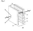
- Fig. 1 is a perspective view of a layered polarized diffractive filter 10 according to a first embodiment of the present invention.
- the layered polarized diffractive filter 10 comprises a transparent substrate 11 made of e.g. glass having a refractive index of n s on which a diffractive grating 12 having cyclic concave/convex portions of depth d is formed.
- a thin film of, e.g., ITO is formed as a transparent conductive film 14.
- the filter also has an opposing transparent substrate 13 having a surface on which a transparent conductive film 14 of ITO is also formed.
- an aligning film (not shown) is formed on each single surface of transparent substrates 11, 13, an aligning film (not shown) is formed.
- the aligning film is subjected to an aligning treatment in a direction parallel to a longitudinal direction of the grating of the diffractive grating 12, in other words, in a direction perpendicular to the direction of diffraction of the diffractive grating.
- a liquid crystal material (liquid crystal) 15 is filled in the space between the transparent substrates 11, 13 at the side of opposing the transparent conductive films 14 to thereby constitute a liquid crystal cell.
- phase differences with respect to applied voltages V 0 , V 1 and V 2 can be rendered to be 2 ⁇ ⁇ 1 / ⁇ , 2 ⁇ 2 / ⁇ and 2 ⁇ 3 / ⁇ respectively, for example.
- Such diffractive grating serves as a layered polarized diffractive filter wherein according to applied voltages V 0 , V 1 and V 2 , transmitting wavelengths correspond to ⁇ 1 , ⁇ 2 and ⁇ 3 respectively. Further, it is possible to form a filter wherein according to variable voltages to be applied, wavelengths to be diffraction-shielded vary.
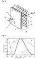
- the layered polarized diffractive filter 20 is similar to the layered polarized diffractive filter 10 in the first embodiment of the present invention except that diffractive gratings 22, 24 are formed on opposing surfaces of transparent substrates 21, 23 respectively so that longitudinal directions of the gratings orthogonally intersect each other.
- the diffractive grating 24 of the same structure as the diffractive grating 22 on the transparent substrate 21 is also formed on the opposing transparent substrate 23.
- These diffractive gratings 22, 24 are subjected to an aligning treatment in a direction parallel to each grating in the same manner as the first embodiment whereby the liquid crystal has a substantially 90° twisted (rotated) structure. Therefore, the filter serves also as an optical rotor.
- the alignment of the liquid crystal means the alignment of liquid crystal molecules. This is applicable to further embodiments.
- the diffractive grating 22 on the transparent substrate 21 provides the same transmission characteristics as the first embodiment under the refractive index n s of the transparent substrate 21 and the extraordinary index n e parallel to a longitudinal direction of the grating of a liquid crystal material 26. Due to the twisted (rotated) structure of the liquid crystal disposed between the opposing transparent substrates 21, 23, the incident linear polarized light is rotated by about 90°. Accordingly, there appear in the diffractive grating 24 on the transparent substrate 23 the same transmission characteristics as the transparent substrate 21 under the transparent substrate 23 and the extraordinary index n e parallel to a longitudinal direction of the grating of the liquid crystal material 26.
- transmittances at this diffractive grating with respect to wavelengths ⁇ 1 , ⁇ 2 and ⁇ 3 are T 1 , T 2 and T 3 (T 1 >T 2 >T 3 ) respectively.
- transmittances are T 1 2 , T 2 2 and T 3 2 (T 1 2 >>T 2 2 >>T 3 2 ).
- the direction of alignment of the liquid crystal is perpendicular to each transparent substrate 21 or 23 whereby there appear in both diffractive gratings 22, 24 transmission characteristics under the refractive indices n s of the transparent substrates 21, 23 and the ordinary index n o of the liquid crystal material to thereby increase the extinction ratio (in this case, however, the liquid crystal does not function as an optical rotor).
- Fig. 3 shows filtering characteristics of this embodiment.
- a solid line A indicates the transmittance when no voltage is applied
- a dotted line B and a broken line C indicate transmittances when voltages V 1 and V 2 (V 1 ⁇ V 2 ) are applied respectively.
- V 1 and V 2 V 1 ⁇ V 2
- Fig. 3 it is understood that when an applied voltage is gradually increased, the wavelength to be transmitted shifts to a side of short wavelength.
- the layered polarized diffractive filter 30 of this embodiment is different from that of the second embodiment in the following points.
- the refractive index of a material constituting either diffractive grating 32 (or 34) is equal to the extraordinary index and the refractive index of a material of the other grating 34 (or 32) is equal to the ordinary index in the diffractive gratings 32, 34 each having cyclic concave/convex portions formed on transparent substrates 31, 33 respectively.
- the following point is different from the second embodiment.
- the direction of alignment of the liquid crystal 36 is parallel to a longitudinal direction of the grating of either diffractive grating 32 (or 34) and is perpendicular to the longitudinal direction of the grating of the other diffractive grating 34 (or 32).
- the diffractive grating 32 and the diffractive grating 34 show substantially the same change of phase difference. Accordingly, it is possible to change the phase difference i.e. the transmittance equally in response to all polarization states of incident light.
- the diffractive grating or diffractive gratings are formed by a photolithography process. Accordingly, it is possible to form a filter in a specified portion corresponding to a light incident region, and it is easy to change the longitudinal direction, depth, cycle and so on of the grating or gratings depending on regions.
- the diffractive filter in any of the first to third embodiments can be installed in an optical system of an optical disk device employing light of, for example, a wavelength bands of 405 nm, 660 nm and 790 nm in combination so as to be used as a wavelength selective filter to transmit light having a wavelength usable for all or a part of the effective region and diffraction-shield light of unused wavelength.
- the diffractive filter can be used as a variable filter capable of treating, for example, wavelength bands of 450 nm, 550 nm and 650 nm for blue, green and red in an image display unit or an image reading unit employing light of visible region.
- the layered polarized diffractive filter 40 is the same as the layered polarized diffractive filter 20 (see Fig. 2) according to the second embodiment of the present invention except the following point.
- the layered polarized diffractive filter 20 comprises the diffractive gratings 22, 24 having substantially the same characteristics whereas in the layered polarized diffractive filter of this embodiment, diffractive gratings 42, 44 having different characteristics are formed on opposing surfaces of transparent substrates 41, 43 respectively so that longitudinal directions of the gratings intersect orthogonally each other.
- the diffractive grating. 44 having a different structure, i.e., different characteristics from the diffractive grating 42 formed on the transparent substrate 41, is formed on the opposing transparent substrate 43.
- These diffractive gratings 42, 44 are subjected to an aligning treatment in a direction parallel to the gratings in the same manner as the first embodiment, whereby the alignment of the liquid crystal has a substantially 90° twisted (rotated) structure of alignment in the same manner as the layered polarized diffractive filter 20 of the second embodiment, hence, it serves as an optical rotor.
- the diffractive grating 42 formed on the transparent substrate 41 provides transmission characteristics under the refractive index n s of the transparent substrate 41 and the extraordinary index n e parallel to a longitudinal direction of the grating of the liquid crystal material 46, in the same manner as the first embodiment.
- the incident linear polarized light rotates by about 90° due to the twisted (rotated) structure of alignment of the liquid crystal between the opposed transparent substrates 41 and 43.
- the refractive grating 44 on the opposing transparent substrate 43 also provides transmission characteristics under the transparent substrate 43 and the extraordinary index n e parallel to a longitudinal direction of the grating of the liquid crystal material 46, in the same manner as the transparent substrate 41.
- phase difference ⁇ determining the transmittance of transmitted light with respect to linear polarized light incident into the interface of the cyclic concave/convex portions of the liquid crystal cell changes from formula 1 to formula 2 in the same manner as the first embodiment.
- phase differences with respect to applied voltages of, for example, V 0 , V 1 and V 2 can be rendered to be 2 ⁇ 1 / ⁇ , 2 ⁇ 2 / ⁇ and 2 ⁇ 3 / ⁇ in the first diffractive grating and 2 ⁇ (2 ⁇ 1 / ⁇ ), 2 ⁇ (2 ⁇ 2 / ⁇ ) and 2 ⁇ (2 ⁇ 3 / ⁇ ) in the second diffractive grating.
- the full width at half maximum of the wavelength of the transmission spectrum in the second diffractive grating at or around a peak wavelength transmitted is narrower than the full width at half maximum of the wavelength of the transmission spectrum in the first diffractive grating, whereby color purity is improved.
- the phase difference of the first diffractive grating may not always be equal to the phase difference of the second diffractive grating but they may be integral multiples of a wavelength to be transmitted.
- the phase difference is preferred to be smaller in order to prevent a reduction of the transmittance or to suppress the number of transmission peaks of a wavelength other than an intended wavelength to be transmitted in a case that the phase difference is increased with integral multiples of the wavelength.
- it is most preferable for the phase differences of the two diffractive gratings to be in a combination of one time and two times of a wavelength to be transmitted, as described above.
- phase differences assuring that a voltage V 0 is applied across two transparent conductive films 45 for example, and transmittances of light having wavelengths of ⁇ 1 , ⁇ 2 and ⁇ 3 at the first diffractive grating 42 are T 1 1 , T 1 2 and T 1 3 , and transmittances of light having wavelengths of ⁇ 1 , ⁇ 2 and ⁇ 3 at the second diffractive grating 44 are T 2 1 , T 2 2 and T 2 3 .
- transmission characteristics of the device according to the fourth embodiment are T 1 1 ⁇ T 1 2 , T 1 2 ⁇ T 2 2 and T 1 3 ⁇ T 3 2 respectively.
- Fig. 6 shows an example of the filtering characteristics of this embodiment.
- a dotted line A indicates the transmittance of the first diffractive grating and a broken line B indicates the transmittance of the second diffractive grating respectively.
- a solid line C indicates the transmittance of a layered structure comprising two diffractive gratings whose longitudinal directions of grating intersect orthogonally. From this figure, it is understood that the full width at half maximum at or around a peak wavelength of transmitted light is made narrow.
- a quartz glass substrate having a refractive index of 1.46 is employed as the transparent substrate 11.
- a diffractive grating 12 having a grating period of 10 ⁇ m and a depth of 2 ⁇ m is formed in a surface of the quartz glass substrate by a photolithography process.
- ITO films of 20 nm thick are formed by sputtering on the diffractive grating 12 and the opposing transparent substrate 13.
- a polyimide resin is coated on them followed by baking and an aligning treatment by rubbing is conducted so that the direction of alignment is parallel to the direction of the grating 12 to thereby form aligning films (not shown).
- a peripheral seal (not shown) of epoxy containing glass fiber spacers of 10 ⁇ m is formed by printing on a peripheral portion of the transparent substrate 13, and then, this transparent substrate is pressure-bonded by applying heat to the transparent substrate 11 so that the directions of alignment are parallel to each other to thereby form a liquid crystal cell.
- liquid crystal 15 having an extraordinary index of 1.76 and an ordinary index of 1.51 is injected by a vacuum injection method and sealed to thereby form the laminated polarized diffractive filter 10.
- the filter When a rectangular a.c. voltage having a frequency of 1 kHz is applied across the transparent electrodes 14, the applied voltage being changed, a peak of the wavelength of transmitted light shifts gradually to a side of short wavelength. Under an applied voltage of about 3 V, the filter transmits 85% or more of light having a wavelength of 450 nm, and the transmittance of light having a wavelength of 650 nm is 15% or less. The light intensity of randomly incident polarized light is reduced to half by the polarizer disposed in front of the filter. However, the coefficient of utilization with respect to transmitted wavelength is about 40%.
- a glass substrate having a refractive index of 1.51 is employed as the transparent substrate 31.
- a SiON film having a thickness of 2.6 ⁇ m and having a composition ratio adjusted so as to be substantially equal to an ordinary index 1.51 of a liquid crystal material used is formed on a surface of the glass substrate by a plasma CVD method.
- a SiON film having a thickness of 2.6 ⁇ m and having a different composition ratio adjusted so as to be substantially equal to an extraordinary index 1.76 of the liquid crystal material used is formed in the same manner as above.
- diffractive gratings 32, 34 each having a grating period of 25 ⁇ m and a depth of 2.6 ⁇ m are formed by a photolithography process.
- transparent conductive films 35 ITO films having a thickness of 20 nm are formed on the diffractive gratings 32 and 34 by a sputtering method respectively.
- aligning films (not shown), a polyimide resin is coated on them followed by baking and an aligning treatment by rubbing is conducted so that the direction of alignment is parallel to a longitudinal direction of the grating with respect to the diffractive grating 32 and the direction of alignment is perpendicular to a longitudinal direction of the grating with respect to the diffractive grating 34.
- a peripheral seal (not shown) of epoxy containing glass fiber spacers of 10 ⁇ m is formed by printing on a peripheral portion of the transparent substrate 33 and both transparent substrates 31, 33 are pressure-bonded by applying heat so that directions of alignment of opposing gratings are parallel, whereby a liquid crystal cell is formed.
- liquid crystal 36 having an extraordinary index of 1.76 and an ordinary index of 1.51 is injected by a vacuum injection method and sealed to thereby form the layered polarized diffractive filter 30.
- the diffractive gratings 32 and 34 act independently on orthogonally intersecting linear polarized light. Accordingly, when polarized light is randomly incident into the liquid crystal cell and when no voltage is applied thereto, it shows a high transmittance as 85% or more with respect to light having a wavelength of 650 nm. On the other hand, it shows a low transmittance as 10% or less with respect to light having a wavelength of 450 nm. When a rectangular a.c. voltage having a frequency of 1 kHz is applied across the two transparent conductive films 35, a peak of the wavelength transmitted shifts gradually to a side of short wavelength.
- the filter transmits 85% or more of light having a wavelength of 450 nm and the transmittance of light having a wavelength of 650 nm is 10% or less. Since there is no polarizer disposed in front of the filter unlike Example 1, the coefficient of utilization with respect to transmitted wavelength is about 80%.
- a glass substrate having a refractive index of 1.51 is employed as the transparent substrate 41.
- an ITO film having a thickness of 20 nm is formed uniformly on a surface of the glass substrate by a sputtering method.
- a Ta 2 O 5 film having a refractive index of about 2.2 and a thickness of 1.2 ⁇ m is formed by a vacuum deposition method.
- an ITO film having a thickness of 20 nm and a Ta 2 O 5 film having a refractive index of about 2.2 and a thickness of 2.4 ⁇ m are formed, as the transparent conductive film 45 sequentially as well.
- a diffractive grating 42 having a grating period of 2 ⁇ m and a depth of 1.2 ⁇ m and a diffractive grating 44 having a grating period of 2 ⁇ m and a depth of 2.4 ⁇ m are formed respectively by a photolithography method.
- a polyvinyl cinnamate resin to align liquid crystal in a polarization direction of ultraviolet light irradiated is coated followed by baking and an aligning treatment by irradiating polarized ultraviolet light is conducted to the coated film so that the direction of alignment is parallel to a longitudinal direction of the grating with respect either to the diffractive grating 42 or the diffractive grating 44 to thereby form aligning films (not shown) .
- a peripheral seal (not shown) of epoxy containing glass fiber spacers of 10 ⁇ m is printed on a peripheral portion of the transparent substrate 43 and these transparent substrates 41, 43 are pressure-bonded by applying heat so that the longitudinal direction of the opposing gratings and the direction of alignment intersect orthogonally, whereby a liquid crystal cell is formed.
- liquid crystal 46 having an extraordinary index of 1.76 and an ordinary index of 1.51 is injected by a vacuum injection method and sealed to thereby form the layered polarized diffractive filter 40.
- the present invention is not limited to the above-mentioned Examples and can be achieved in various modes unless they deviate from the sprit of the present invention.
- the wavelength to be transmitted or diffraction-shielded can be changed.
- the diffractive filter of the present invention can be employed in an optical head device for recording or reading data to an optical disk using a large number of wavelengths or can be used as a part of an image displaying device or an image processing device using a wavelength range covering the whole visible light region, whereby a device of simple, smaller number of component elements, small-sized and reduced weight can be obtained.
Applications Claiming Priority (2)
| Application Number | Priority Date | Filing Date | Title |
|---|---|---|---|
| JP2004221265 | 2004-07-29 | ||
| PCT/JP2005/013766 WO2006011530A1 (fr) | 2004-07-29 | 2005-07-27 | Filtre de diffraction polarisé et filtre de diffraction polarisé en couches |
Publications (2)
| Publication Number | Publication Date |
|---|---|
| EP1780582A1 true EP1780582A1 (fr) | 2007-05-02 |
| EP1780582A4 EP1780582A4 (fr) | 2009-07-08 |
Family
ID=35786280
Family Applications (1)
| Application Number | Title | Priority Date | Filing Date |
|---|---|---|---|
| EP05767354A Withdrawn EP1780582A4 (fr) | 2004-07-29 | 2005-07-27 | Filtre de diffraction polarisé et filtre de diffraction polarisé en couches |
Country Status (7)
| Country | Link |
|---|---|
| US (1) | US7623291B2 (fr) |
| EP (1) | EP1780582A4 (fr) |
| JP (1) | JP4826472B2 (fr) |
| KR (1) | KR101098202B1 (fr) |
| CN (1) | CN1989441A (fr) |
| TW (1) | TW200615583A (fr) |
| WO (1) | WO2006011530A1 (fr) |
Cited By (2)
| Publication number | Priority date | Publication date | Assignee | Title |
|---|---|---|---|---|
| EP2700987A1 (fr) * | 2012-08-24 | 2014-02-26 | JDS Uniphase Corporation | Retardateur optique variable |
| US9588374B2 (en) | 2014-02-19 | 2017-03-07 | Lumentum Operations Llc | Reflective LC devices including thin film metal grating |
Families Citing this family (16)
| Publication number | Priority date | Publication date | Assignee | Title |
|---|---|---|---|---|
| WO2003025633A1 (fr) * | 2001-09-13 | 2003-03-27 | Asahi Glass Company, Limited | Dispositif de diffraction |
| US7729226B2 (en) * | 2003-10-06 | 2010-06-01 | Ricoh Company, Ltd. | Wavefront aberration compensation element, optical pickup, and optical disk apparatus |
| EP1780582A4 (fr) | 2004-07-29 | 2009-07-08 | Asahi Glass Co Ltd | Filtre de diffraction polarisé et filtre de diffraction polarisé en couches |
| TW200638101A (en) * | 2005-02-02 | 2006-11-01 | Asahi Glass Co Ltd | The devices of light flux changing and projected display apparatus |
| KR20080084964A (ko) * | 2005-12-15 | 2008-09-22 | 아사히 가라스 가부시키가이샤 | 파장 선택 회절 소자 및 광 헤드 장치 |
| KR101330860B1 (ko) * | 2007-12-27 | 2013-11-18 | 아사히 가라스 가부시키가이샤 | 액정 소자 및 광 헤드 장치 및 가변 광 변조 소자 |
| CN102654654A (zh) * | 2011-11-14 | 2012-09-05 | 京东方科技集团股份有限公司 | 一种3d显示器件及其制造方法 |
| EP2965134A1 (fr) * | 2013-03-05 | 2016-01-13 | Rambus Inc. | Réseaux de phase ayant une symétrie impaire pour détection optique sans lentille haute résolution |
| KR101395024B1 (ko) * | 2013-03-14 | 2014-05-27 | 광운대학교 산학협력단 | 능동 스펙트럼 필터링 장치 |
| JP2016065964A (ja) * | 2014-09-24 | 2016-04-28 | 株式会社デンソー | 光学部品 |
| KR102466673B1 (ko) * | 2016-01-13 | 2022-11-14 | 삼성전자주식회사 | 가변 전기광학 필터 |
| TWI645218B (zh) * | 2017-07-20 | 2018-12-21 | Benq Materials Corporation | 光重導向膜 |
| CN107577093B (zh) * | 2017-09-20 | 2020-12-01 | 京东方科技集团股份有限公司 | 一种显示模组及光波导显示装置 |
| WO2021167657A2 (fr) | 2019-11-13 | 2021-08-26 | Lumotive, LLC | Systèmes lidar à base de métasurfaces optiques accordables |
| CN111221068B (zh) * | 2020-01-21 | 2021-11-09 | 东南大学 | 一种基于亚波长光栅结构的起偏器 |
| US11487183B1 (en) * | 2022-03-17 | 2022-11-01 | Lumotive, LLC | Tunable optical device configurations and packaging |
Citations (3)
| Publication number | Priority date | Publication date | Assignee | Title |
|---|---|---|---|---|
| US4251137A (en) * | 1977-09-28 | 1981-02-17 | Rca Corporation | Tunable diffractive subtractive filter |
| US4729640A (en) * | 1984-10-03 | 1988-03-08 | Canon Kabushiki Kaisha | Liquid crystal light modulation device |
| WO1996027148A1 (fr) * | 1995-02-28 | 1996-09-06 | Philips Electronics N.V. | Dispositif electro-optique |
Family Cites Families (14)
| Publication number | Priority date | Publication date | Assignee | Title |
|---|---|---|---|---|
| JPS6186727A (ja) * | 1984-10-04 | 1986-05-02 | Canon Inc | 光制御素子 |
| JPS62235926A (ja) * | 1986-04-07 | 1987-10-16 | Canon Inc | 光変調素子 |
| JPH08278477A (ja) * | 1994-12-27 | 1996-10-22 | Seiko Epson Corp | 回折素子、光ヘッド及び光記録再生装置 |
| JP3711652B2 (ja) * | 1996-06-18 | 2005-11-02 | 旭硝子株式会社 | 偏光回折素子及びそれを用いた光ヘッド装置 |
| JP4281187B2 (ja) | 1999-03-31 | 2009-06-17 | 旭硝子株式会社 | 光ヘッド装置 |
| JP4345256B2 (ja) | 2001-02-14 | 2009-10-14 | 旭硝子株式会社 | 波長選択性回折素子および光ヘッド装置 |
| WO2003019247A1 (fr) | 2001-08-24 | 2003-03-06 | Asahi Glass Company, Limited | Polariseur multicouches a diffraction et element a cristaux liquides |
| WO2003025633A1 (fr) | 2001-09-13 | 2003-03-27 | Asahi Glass Company, Limited | Dispositif de diffraction |
| JPWO2004081620A1 (ja) | 2003-03-13 | 2006-06-15 | 旭硝子株式会社 | 回折素子および光学装置 |
| JPWO2004097816A1 (ja) | 2003-04-25 | 2006-07-13 | 旭硝子株式会社 | 回折素子および光ヘッド装置 |
| JP4561080B2 (ja) | 2003-11-07 | 2010-10-13 | 旭硝子株式会社 | 回折素子および光ヘッド装置 |
| JP5055694B2 (ja) | 2003-12-26 | 2012-10-24 | 旭硝子株式会社 | 偏光性回折素子および光ヘッド装置 |
| EP1780582A4 (fr) | 2004-07-29 | 2009-07-08 | Asahi Glass Co Ltd | Filtre de diffraction polarisé et filtre de diffraction polarisé en couches |
| TW200638101A (en) | 2005-02-02 | 2006-11-01 | Asahi Glass Co Ltd | The devices of light flux changing and projected display apparatus |
-
2005
- 2005-07-27 EP EP05767354A patent/EP1780582A4/fr not_active Withdrawn
- 2005-07-27 CN CNA2005800251386A patent/CN1989441A/zh active Pending
- 2005-07-27 JP JP2006527831A patent/JP4826472B2/ja active Active
- 2005-07-27 WO PCT/JP2005/013766 patent/WO2006011530A1/fr active Application Filing
- 2005-07-27 KR KR1020077000554A patent/KR101098202B1/ko active IP Right Grant
- 2005-07-29 TW TW094125919A patent/TW200615583A/zh unknown
-
2007
- 2007-01-26 US US11/627,720 patent/US7623291B2/en not_active Expired - Fee Related
Patent Citations (3)
| Publication number | Priority date | Publication date | Assignee | Title |
|---|---|---|---|---|
| US4251137A (en) * | 1977-09-28 | 1981-02-17 | Rca Corporation | Tunable diffractive subtractive filter |
| US4729640A (en) * | 1984-10-03 | 1988-03-08 | Canon Kabushiki Kaisha | Liquid crystal light modulation device |
| WO1996027148A1 (fr) * | 1995-02-28 | 1996-09-06 | Philips Electronics N.V. | Dispositif electro-optique |
Non-Patent Citations (1)
| Title |
|---|
| See also references of WO2006011530A1 * |
Cited By (5)
| Publication number | Priority date | Publication date | Assignee | Title |
|---|---|---|---|---|
| EP2700987A1 (fr) * | 2012-08-24 | 2014-02-26 | JDS Uniphase Corporation | Retardateur optique variable |
| US9946134B2 (en) | 2012-08-24 | 2018-04-17 | Lumentum Operations Llc | Variable optical retarder |
| US10747044B2 (en) | 2012-08-24 | 2020-08-18 | Lumentum Operations Llc | Variable optical retarder |
| US9588374B2 (en) | 2014-02-19 | 2017-03-07 | Lumentum Operations Llc | Reflective LC devices including thin film metal grating |
| US10473839B2 (en) | 2014-02-19 | 2019-11-12 | Lumentum Operations Llc | Reflective LC devices including thin film metal grating |
Also Published As
| Publication number | Publication date |
|---|---|
| KR20070055485A (ko) | 2007-05-30 |
| TW200615583A (en) | 2006-05-16 |
| EP1780582A4 (fr) | 2009-07-08 |
| JP4826472B2 (ja) | 2011-11-30 |
| CN1989441A (zh) | 2007-06-27 |
| JPWO2006011530A1 (ja) | 2008-05-01 |
| US20070121210A1 (en) | 2007-05-31 |
| US7623291B2 (en) | 2009-11-24 |
| WO2006011530A1 (fr) | 2006-02-02 |
| KR101098202B1 (ko) | 2011-12-23 |
Similar Documents
| Publication | Publication Date | Title |
|---|---|---|
| US7623291B2 (en) | Polarized diffractive filter and layered polarized diffractive filter | |
| US10509296B2 (en) | Compact liquid crystal beam steering devices including multiple polarization gratings | |
| EP1420275B1 (fr) | isolateur et atténuateur optique | |
| US7405786B2 (en) | Laminated retardation optical element, process of producing the same, and liquid crystal display | |
| US9575366B2 (en) | Fast switchable and high diffraction efficiency grating ferroelectric liquid crystal cell | |
| WO2006023528A2 (fr) | Filtre d'imagerie spectrale accordable conçu pour des plages spectrales d'uv | |
| KR20060104994A (ko) | 광학적 등방성을 갖는 액정을 사용한 광학 소자 | |
| US20020036735A1 (en) | Collimator and backlight system | |
| KR950029815A (ko) | 컬러액정표시장치 | |
| KR100744818B1 (ko) | 위상차 광학소자와 그 제조방법 및 액정표시장치 | |
| EP3650927B1 (fr) | Dispositif de commutation optique à grande vitesse | |
| JP2006215186A (ja) | 回折素子とその製造方法および回折素子を用いた偏光選択装置 | |
| JP4269788B2 (ja) | 反射型光変調素子および可変光減衰器 | |
| JP4106981B2 (ja) | 光減衰器 | |
| JP4377633B2 (ja) | 位相差光学素子、その製造方法及び液晶表示装置 | |
| JP4984389B2 (ja) | 横電界駆動液晶セルおよびそれを用いた波長可変フィルタ | |
| JP5150992B2 (ja) | 液晶素子および光減衰器 | |
| JP2002258053A (ja) | 円偏光抽出光学素子及びその製造方法、偏光光源装置、液晶表示装置 | |
| JP2004145268A (ja) | 位相差光学素子及びその製造方法、並びに位相差光学素子を備えた偏光素子及び液晶表示装置 | |
| JP2004325790A (ja) | 光変調素子および光減衰器 | |
| JP2004347784A (ja) | 反射型光学素子 | |
| JP4786841B2 (ja) | 液晶光スイッチとその駆動方法 | |
| CN114902124A (zh) | 太赫兹波控制元件 | |
| JP2006154492A (ja) | 液晶素子および光減衰器 | |
| WO2002048802A1 (fr) | Dispositif holographique commutable |
Legal Events
| Date | Code | Title | Description |
|---|---|---|---|
| PUAI | Public reference made under article 153(3) epc to a published international application that has entered the european phase |
Free format text: ORIGINAL CODE: 0009012 |
|
| 17P | Request for examination filed |
Effective date: 20070208 |
|
| AK | Designated contracting states |
Kind code of ref document: A1 Designated state(s): AT BE BG CH CY CZ DE DK EE ES FI FR GB GR HU IE IS IT LI LT LU LV MC NL PL PT RO SE SI SK TR |
|
| DAX | Request for extension of the european patent (deleted) | ||
| A4 | Supplementary search report drawn up and despatched |
Effective date: 20090605 |
|
| 17Q | First examination report despatched |
Effective date: 20090929 |
|
| RAP1 | Party data changed (applicant data changed or rights of an application transferred) |
Owner name: ASAHI GLASS COMPANY, LIMITED |
|
| STAA | Information on the status of an ep patent application or granted ep patent |
Free format text: STATUS: THE APPLICATION IS DEEMED TO BE WITHDRAWN |
|
| 18D | Application deemed to be withdrawn |
Effective date: 20130201 |