EP1779516B1 - Master-slave-flipflop für einen empfangsoszillator und mischer in einer i/q-schaltung - Google Patents
Master-slave-flipflop für einen empfangsoszillator und mischer in einer i/q-schaltung Download PDFInfo
- Publication number
- EP1779516B1 EP1779516B1 EP05773300A EP05773300A EP1779516B1 EP 1779516 B1 EP1779516 B1 EP 1779516B1 EP 05773300 A EP05773300 A EP 05773300A EP 05773300 A EP05773300 A EP 05773300A EP 1779516 B1 EP1779516 B1 EP 1779516B1
- Authority
- EP
- European Patent Office
- Prior art keywords
- latches
- channel
- channels
- latch
- frequency
- Prior art date
- Legal status (The legal status is an assumption and is not a legal conclusion. Google has not performed a legal analysis and makes no representation as to the accuracy of the status listed.)
- Expired - Lifetime
Links
Images


Classifications
-
- H—ELECTRICITY
- H03—ELECTRONIC CIRCUITRY
- H03D—DEMODULATION OR TRANSFERENCE OF MODULATION FROM ONE CARRIER TO ANOTHER
- H03D7/00—Transference of modulation from one carrier to another, e.g. frequency-changing
- H03D7/16—Multiple-frequency-changing
- H03D7/165—Multiple-frequency-changing at least two frequency changers being located in different paths, e.g. in two paths with carriers in quadrature
- H03D7/166—Multiple-frequency-changing at least two frequency changers being located in different paths, e.g. in two paths with carriers in quadrature using two or more quadrature frequency translation stages
-
- H—ELECTRICITY
- H03—ELECTRONIC CIRCUITRY
- H03K—PULSE TECHNIQUE
- H03K23/00—Pulse counters comprising counting chains; Frequency dividers comprising counting chains
- H03K23/40—Gating or clocking signals applied to all stages, i.e. synchronous counters
- H03K23/50—Gating or clocking signals applied to all stages, i.e. synchronous counters using bi-stable regenerative trigger circuits
- H03K23/54—Ring counters, i.e. feedback shift register counters
-
- H—ELECTRICITY
- H03—ELECTRONIC CIRCUITRY
- H03K—PULSE TECHNIQUE
- H03K23/00—Pulse counters comprising counting chains; Frequency dividers comprising counting chains
- H03K23/40—Gating or clocking signals applied to all stages, i.e. synchronous counters
- H03K23/50—Gating or clocking signals applied to all stages, i.e. synchronous counters using bi-stable regenerative trigger circuits
- H03K23/54—Ring counters, i.e. feedback shift register counters
- H03K23/542—Ring counters, i.e. feedback shift register counters with crossed-couplings, i.e. Johnson counters
Definitions
- the present invention relates to circuitry used in an integrated circuit (IC), and more particularly to circuitry used in generating frequencies used for processing of quadrature signals.
- IC integrated circuit
- a down conversion process occurs in which a received signal at a very high frequency, such as a radio frequency (RF) is received and processed to obtain a lower frequency signal to be used for further processing.
- RF radio frequency
- Such lower frequency signals may include an intermediate frequency (IF) signal, such as a low IF signal.
- IF intermediate frequency
- a RF signal may be directly downconverted to a zero IF signal.
- such down conversion is effected by taking a received signal at a first frequency (typically RF) and mixing it with a local oscillator (LO) frequency to obtain a desired IF or other lower frequency signal.
- a first frequency typically RF
- LO local oscillator
- the LO frequency may be generated using a crystal oscillator or other such reference frequency generator.
- such a frequency is provided to a frequency divider, where the reference frequency is divided by either a fixed or programmable amount. The divided frequency may then be provided to a mixer for mixing with a received signal.
- an odd number factor frequency divider is formed of a plurality of cascade-connected master-slave D-type flip-flops, operating from a common clock signal, with a single NOR gate being used to derive a signal expressing the negated logic sum of the respective Q-terminal logic outputs from the master D-type latch and the slave S-type latch which constitute the final-stage flip-flop of the plurality of cascade-connected flip-flops.
- JP 2003 133946 A provides a T-type flip-flop dividing circuit of the emitter coupled logic type or the collector coupled logic type which consists of a master flip-flop and a slave flip-flop. Emitter sizes of the input differential pair transistors of the master flip-flop and/or the slave flip-flop are different.
- the LO signals provided to the mixer are preferably low noise signals, as the noise created in generating the LO frequency such as via a frequency divider and a voltage controlled oscillator (VCO) can adversely affect receiver performance.
- VCO voltage controlled oscillator
- a divide by two frequency divider is present, noise and other interference may exist, such as second harmonics of the divided frequency.
- Such frequency dividers also suffer from noise problems and require a high frequency VCO with buffers capable of driving large capacitances at high frequencies, such that the VCO consumes high power.
- outputs from such a frequency divider may be jittery, causing a modulation in terms of phase that may appear as phase noise.
- a frequency divider used in developing a LO frequency should be well matched between its I and Q sides, as mismatches can cause a phase error and therefore image rejection degradation.
- the image rejection of a frequency divider refers to the ability to reject responses resulting from RF signals at a frequency offset from the desired RF carrier frequency by an amount equal to twice the IF of the receiver.
- a frequency divider should be well shielded, as 45 phase-shifted signals are present inside the frequency divider and an asymmetric coupling between the signals can cause degradation. Also, a frequency divider should consume low power, particularly where the circuitry operates at gigahertz frequencies.
- the invention provides an apparatus according to the subject-matter of independent claim 1. Another aspect of the invention is directed to a method of generating frequencies for processing of quadrature signals, according to the subject-matter of independent claim 15. Further aspects and embodiments of the invention are set forth in the dependent claims, the following description and the drawings.
- the present invention includes a frequency divider that has an I channel master storage element formed of devices of a first size and an I channel slave storage element coupled to an output of the I channel master storage element formed of devices of a second size, where the second size is smaller than the first size.
- the frequency divider also includes a Q channel master storage element coupled to an output of the I channel slave storage element formed of devices of the first size and a Q channel slave storage element coupled to an output of the Q channel master storage element formed of devices of the second size.
- the present invention includes an apparatus having a frequency divider with a first I channel having first and second latches and a first Q channel coupled to the first I channel having first and second latches, where the first latches are stronger than the second latches.
- the frequency divider may provide outputs to a quadrature mixer for mixing with incoming RF signals.
- a system such as a cellular telephone including a transceiver, which may be of a GSM/GPRS system having first I and Q channels of a frequency divider each having first and second latches, where the first latches are larger than the second latches.
- the transceiver may further include first I and Q channel mixers to receive I and Q channel phases from the first I and Q channels of the frequency divider.
- the frequency divider may further include second I and Q channels having third and fourth latches, where the third latches are larger than the fourth latches.
- the system may include second I and Q channel mixers to receive I and Q channel phases from the second I and Q channels of the frequency divider.
- the system may further include an antenna coupled to the transceiver to receive and transmit information and a processor coupled to the transceiver to process the information.
- Such a system may operate at high frequencies with reduced power consumption while reducing phase noise between the different phases generated by the I and Q channels.
- Still another embodiment of the present invention includes generating I and Q channel clean outputs from jittery inputs.
- the jittery inputs may be caused by latches formed of weaker devices, while latches formed of stronger devices may be used to generate the clean outputs.
- the clean outputs may be provided to a mixer for use in mixing with incoming RF signals.
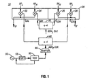
- FIG. 1 shown is a block diagram of a portion of a system in accordance with one embodiment of the present invention. More specifically, as shown in FIG. 1 , a local oscillator and mixer portion of a system is shown. As used herein, the term "lomix" refers to a local oscillator and a mixer. As shown in FIG. 1 , lomix 10 includes a quadrature mixer 20, a first frequency divider 30, and a second frequency divider 40. As shown in the embodiment of FIG. 1 , frequency dividers 30 and 40 may be divide by four frequency dividers, although the scope of the present invention is not so limited.
- phase locked loop PLL
- a fractional-N PLL may be present to provide different frequencies to buffer 65.
- lomix 10 may receive RF signals on either a low frequency RF input (RF L ) or a high frequency RF input (RF H ). Such signals may be provided to both an I channel and a Q channel of quadrature mixer 20.
- high RF signals may be at a frequency of between approximately 1.8 and 2 gigahertz (GHz).
- GHz gigahertz
- high RF signals may be at a frequency of approximately 1.9 GHz for a Personal Communication System (PCS), or at approximately a 1.84 GHz frequency for a Digital Cellular System (DCS), although the scope of the present invention is not so limited.
- low RF signals may be at a frequency of between approximately 800 megahertz (GHz) to one GHz.
- low RF signals may be at a frequency of approximately 850 MHz for a Global System for Mobile Communications (GSM) system, or at a 900 MHz frequency for a cellular telephone using an Extended GSM (EGSM) system, although the scope of the present invention is not so limited.
- GSM Global System for Mobile Communications
- EGSM Extended GSM
- low RF signals may be coupled to an I channel mixer 22 and a Q channel mixer 28, while high RF signals may be coupled to an I channel mixer 24 and a Q channel mixer 26.
- outputs of frequency divider 40 i.e., I LOL and Q LOL .
- I and Q mixers 22 and 28 may mix the incoming signals with the respective LO frequency to obtain respective IF signals, namely I IF and Q IF .
- the outputs of frequency divider 40 may be a 1 GHz LO frequency. That is, as shown in FIG. 1 , frequency divider 40 may receive a buffered clock signal of 4 GHz and in turn output quadrature LO signals of 1 GHz.
- a different LO frequency may be provided to mixers 22 and 28 to generate IF signals of different frequencies.
- low IF signals of approximately 100 to 300 kilohertz (KHz) may be generated and provided to other circuitry for further processing.
- high RF signals may be coupled to I channel mixer 24 and Q channel mixer 26 for mixing with the outputs of frequency divider 30 (namely I LOH and Q LOH ).
- mixers 24 and 26 may provide quadrature IF signals (namely I IF and Q IF ) for further processing.
- frequency divider 30 may receive a buffered input clock frequency of 8 GHz and generate quadrature LO signals of 2 GHz to I channel mixer 24 and Q channel mixer 26.
- low IF signals may be generated therefrom.
- the low IF signals may be between approximately 100-300 KHz in certain embodiments.
- frequency dividers 30 and 40 may be formed using a combination of strong and weak storage elements, such as latches.
- strong and weak storage elements such as latches.
- larger higher power devices may be used in one portion of the divider, while smaller lower power devices may be used in other portions of the dividers for phases that are not provided out of the frequency dividers. That is, in various embodiments, outputs from stages of a frequency divider to be provided to a quadrature mixer may be generated from strong latches, while stages not being provided out of the frequency divider may be formed of weak latches.
- DFF D-type flip-flops
- a DFF may receive a jittery input. Such an input may be modulated in phase, causing phase noise on the input to the DFF.
- CLK clock input
- a DFF is itself formed of a master latch and a slave latch, and the D-input of the master latch is driven by the output of the slave latch. Therefore, by making a master latch a stronger version of an associated slave latch, power may be saved, and may lead to appreciable power savings at higher operating frequencies.
- frequency divider 30 may be the same as frequency divider 30 of FIG. 1 .
- Frequency divider 30 may be formed of a master latch 32, which is coupled to a slave latch 34, which in turn is coupled to a master latch 36 that in turn is coupled to a slave latch 38.
- the outputs of slave latch 38 may be cross-coupled to the inputs of master latch 32 to form a loop therebetween.
- master latches 32 and 36 may be strong, that is a latch formed using larger devices than the devices used to form slave latches 34 and 38.
- the relative sizes of the devices used to form master latches and slave latches may vary. For example, in an embodiment used in a divide by four circuit that operates at a clock frequency of 8 GHz (i.e., a high RF band), the stronger latches may be approximately two times (2X) the size of the devices that form the slave latches, although the scope of the present invention is not so limited.
- the stronger latches may be approximately three times (3x) the size of the devices that form the slave latches, although the scope of the present invention is not so limited.
- standard deviation e.g., of threshold voltage or beta ( ⁇ )
- CMOS device parameters vary inversely to the area occupied by the device.
- larger devices have a smaller standard deviation than smaller devices.
- larger device geometries may be used for the devices that form the strong latches and provide outputs to an associated quadrature mixer. Accordingly, mismatch in these outputs may be minimized.
- the output of master latches 32 and 36 are clean outputs, meaning the outputs are either free of phase noise or have phase noise substantially reduced because of the size of the devices therein.
- the outputs of slave latches 34 and 38 are jittery outputs, as they suffer from a phase noise penalty.
- the noise is manageable. This is so, as the master latches to which the slaves are coupled can convert the jittery inputs to clean outputs, so long as the master latches are clocked with a clean clock signal.
- slave latches While shown in the embodiment of FIG. 2 with strong master latches and outputs therefrom being provided to the quadrature mixer, in other embodiments the slave latches may be made stronger than the master latches and the outputs therefrom instead routed to the quadrature mixers.
- V T beta and threshold voltage
- the outputs therefrom may be in better quadrature alignment.
- weak latches are used for the slave latches, power consumption may be reduced by more than 30%, particularly in embodiments operating at a RF band.
- weak devices are used for at least certain portions of the frequency divider, parasitic capacitance on clock traces provided to the devices may be reduced, resulting in significant power savings for the buffer that drives the clock signal to the frequency divider.
- Such a transceiver may be a CMOS transceiver for quad-band GSM/GPRS wireless communications such as for use in cellular handsets and wireless data modems, although the scope of the present invention is not so limited.
- incoming RF signals may be received by an antenna 102 and passed to an antenna switch 104. While different embodiments may be used with different RF communication devices, in one embodiment, incoming signals may be RF signals of a cellular telephone, and transceiver 100 may be a single chip transceiver for use in such a cell phone handset. Antenna switch 104 may be used to switch between incoming and outgoing signals from transceiver 100.
- a quad-band receiver may be present.
- a quad-band receiver may be adapted to receive GSM, EGSM, DCS, and PCS signals, although the scope of the present invention is not so limited.
- transceiver 100 may be used in a General Packet Radio Service (GPRS) device, a satellite tuner, or a wireless local area network (WLAN) device, for example.
- GPRS General Packet Radio Service
- WLAN wireless local area network
- Such incoming signals may pass through an external filter 108, such as a receive surface acoustic wave (SAW) filter bank, and be provided into transceiver 100, and more specifically to a low noise amplifier (LNA) 150. While shown as a single LNA, it is to be understood that multiple LNAs may be present to receive signals of the different bands.
- incoming RF signals may be provided to a quadrature mixer 160 having an I channel mixer 162 and a Q channel mixer 164. While shown with single mixers per phase, it is to be understood that quadrature mixer 160 may include multiple mixers for each phase, as shown in FIG. 1 , for example.
- Quadrature mixer 160 may receive I and Q LO inputs from a frequency divider and phase shifter 145, which may correspond to frequency dividers 30 and 40 shown in FIG. 1 .
- the I and Q channels may be routed to respective filters 165a and 165b and programmable gain amplifiers (PGA's) 170a and 170b. From there, the signals may be provided to analog-to-digital converters (ADC's) 175a and 175b for conversion to digital signals. The digital signals may then be provided to an IF block 180, for further downmixing and processing at a low IF frequency. Then the resulting baseband signals may be provided to an analog interface 190 for transmission to baseband components of a handset or other such device. While only the receive path is shown in FIG. 3 , it is to be understood that similar components may be present within transceiver 100 to provide for reception of baseband signals from within the handset or other such device and conversion to RF signals for transmission via antenna 102.
- ADC's analog-to-digital converters
- transceiver 100 may include additional and/or different components, and the embodiment shown in FIG. 3 is for illustrative purposes.
- system 200 may be a cellular telephone handset, although the scope of the present invention is not so limited.
- the system may be a pager, personal digital assistant (PDA) or other such device.
- antenna 102 may be coupled to a transceiver 100, such as the transceiver shown in FIG. 3 .
- transceiver 100 may be coupled to a digital signal processor (DSP) 210, which may handle processing of baseband communication signals.
- DSP digital signal processor
- DSP 210 may be coupled to a microprocessor 220, such as a central processing unit (CPU) that may be used to control operation of system 200 and further handle processing of application programs, such as personal information management (PIM) programs, email programs, downloaded games, and the like.
- microprocessor 200 and DSP 210 may also be coupled to a memory 230.
- Memory 230 may include different memory components, such as a flash memory and a read only memory (ROM), although the scope of the present invention is not so limited.
- a display 240 may be present to provide display of information associated with telephone calls and application programs.
- transceiver 100 may include one or more frequency dividers and quadrature mixers in accordance with an embodiment of the present invention.
Landscapes
- Engineering & Computer Science (AREA)
- Power Engineering (AREA)
- Transceivers (AREA)
- Superheterodyne Receivers (AREA)
Claims (18)
- Vorrichtung, umfassend:einen Frequenzteiler (30) undeinen Quadraturmischer (20),wobei ein erster I-Kanal des Frequenzteilers (30) ein erstes Latch (32) und ein zweites Latch (34) umfasst, wobei das erste Latch (32) mit dem zweiten Latch (34) verbunden ist, und
wobei ein erster, mit dem ersten I-Kanal verbundener Q-Kanal des Frequenzteilers (30) ein erstes Latch (36) und ein zweites Latch (38) umfasst, wobei das erste Latch (36) mit dem zweiten Latch (38) verbunden ist und wobei die ersten Latches (32, 36) des ersten I- und Q-Kanals größer sind als die zweiten Latches (34, 38) des ersten I- und Q-Kanals, und wobei die Ausgänge der ersten Latches (32, 36) des ersten I- und Q-Kanals mit dem Quadraturmischer (20) verbunden sind, um eine geteilte Frequenz bereitzustellen. - Vorrichtung nach Anspruch 1, bei der die Ausgänge der ersten Latches (32, 36) des ersten I- und Q-Kanals im Vergleich zu den Ausgängen der zweiten Latches (34, 38) des ersten I- und Q-Kanals ein verringertes Phasenrauschen aufweisen.
- Vorrichtung nach Anspruch 1, bei der die Ausgänge der ersten Latches (32, 36) des ersten I- und Q-Kanals saubere Ausgänge mit einem reduzierten Phasenrauschen sind und die Ausgänge der zweiten Latches (34, 38) des ersten I- und Q-Kanals Jitter-Ausgänge sind, und
wobei die ersten Latches (32, 36) des ersten I- und Q-Kanals dazu geeignet sind, Jitter-Eingänge zu empfangen und die Jitter-Eingänge in saubere Ausgänge mit reduziertem Phasenrauschen umzuwandeln. - Vorrichtung nach einem der vorangehenden Ansprüche, bei der Ausgänge des zweiten Latches (38) des ersten Q-Kanals kreuzweise mit Eingängen des ersten Latches (32) des ersten I-Kanals verbunden sind.
- Vorrichtung nach einem der vorangehenden Ansprüche, bei der das erste und zweite Latch (32, 34) des ersten I-Kanals und das erste und zweite Latch (36, 38) des ersten Q-Kanals jeweils in einer Master-Slave-Beziehung miteinander verbunden sind.
- Vorrichtung nach Anspruch 1, die außerdem einen Puffer umfasst, der zum Bereitstellen eines gepufferten Taktsignals an den ersten I-Kanal und den ersten Q-Kanal verbunden ist.
- Vorrichtung nach Anspruch 6, die außerdem eine fractional-N Phasenregelschleife umfasst, die zum Bereitstellen eines gesteuerten Taktsignals an den Puffer verbunden ist.
- Vorrichtung nach Anspruch 1, bei die ersten Latches (32, 36) des ersten I- und Q-Kanals aus Einheiten einer ersten Größe gebildet sind und die zweiten Latches (34, 38) des ersten I- und Q-Kanals aus Einheiten einer zweiten Größe gebildet sind, wobei die erste Größe im Wesentlichen größer als die zweite Größe ist.
- Vorrichtung nach Anspruch 1, außerdem umfassend:einen zweiten I-Kanal des Frequenzteilers (30) mit einem dritten Latch und einem vierten Latch, undeinen zweiten, mit dem zweiten I-Kanal verbundenen Q-Kanal des Frequenzteilers (30) mit einem dritten Latch und einem vierten Latch, wobei die dritten Latches des zweiten I- und Q-Kanals größer als die vierten Latches des zweiten I- und Q-Kanals sind.
- Vorrichtung nach Anspruch 9, bei der sich ein erstes Verhältnis zwischen der Größe von Einheiten, welche die ersten Latches (32, 36) und die zweiten Latches (34, 38) bilden, von einem zweiten Verhältnis zwischen der Größe von Einheiten, welche die dritten Latches und die vierten Latches bilden, unterscheidet.
- Vorrichtung nach Anspruch 9, bei der der erste I- und Q-Kanal zum Bereitstellen einer ersten Frequenz an den Quadraturmischer (20) und der zweite I- und Q-Kanal zum Bereitstellen einer zweiten Frequenz an den Quadraturmischer (20) geeignet sind.
- Vorrichtung nach Anspruch 11, bei der der Quadraturmischer (20) die erste Frequenz oder die zweite Frequenz zum Mischen mit einem eingehenden Signal verwendet, basierend auf dem eingehenden Signal.
- Vorrichtung nach einem der vorangehenden Ansprüche, bei der die Vorrichtung einen Transceiver für ein Mobiltelefon umfasst.
- Mobiltelefon, umfassend eine Vorrichtung nach einem der vorangehenden Ansprüche.
- Verfahren zum Erzeugen von Frequenzen zum Verarbeiten von Quadratursignalen, das Verfahren umfassend:Erzeugen eines sauberen I-Kanal-Ausgangs mit reduziertem Phasenrauschen in einer ersten I-Kanal-Stufe eines Frequenzteilers (30) aus einem ersten Jitter-Eingang;Bereitstellen des sauberen I-Kanal-Ausgangs mit dem reduzierten Phasenrauschen an einen Quadraturmischer;Erzeugen eines sauberen Q-Kanal-Ausgangs mit reduziertem Phasenrauschen in einer ersten Q-Kanal-Stufe des Frequenzteilers (30) aus einem zweiten Jitter-Eingang; undBereitstellen des sauberen Q-Kanal-Ausgangs mit reduziertem Phasenrauschen an den Quadraturmischer;wobei die sauberen Ausgänge mit reduziertem Phasenrauschen durch erste Latches (32, 36) der ersten I- und Q-Kanalstufe bereitgestellt werden und die Jitter-Eingänge durch zweite Latches (34, 38) der ersten I- und Q-Kanalstufe bereitgestellt werden, und wobei die ersten Legdes (32, 36) der ersten I- und Q-Kanalstufe größer als die zweiten Latches (34, 38) des ersten I- und Q-Kanals sind.
- Verfahren nach Anspruch 15, außerdem umfassend das Erzeugen des zweiten Jitter-Eingangs in einer zweiten I-Kanal-Stufe des Frequenzteilers (30).
- Verfahren nach Anspruch 16, bei dem die erste I-Kanal-Stufe Einheiten einer ersten Größe und die zweite I-Kanal-Stufe Einheiten einer zweiten Größe umfasst, wobei die erste Größe im Wesentlichen größer als die zweite Größe ist.
- Verfahren nach Anspruch 15, außerdem umfassend das Bereitstellen eines sauberen Taktsignals an die erste I-Kanal-Stufe und die erste Q-Kanal-Stufe.
Applications Claiming Priority (2)
| Application Number | Priority Date | Filing Date | Title |
|---|---|---|---|
| US10/901,508 US7379723B2 (en) | 2004-07-29 | 2004-07-29 | Local oscillator and mixer for transceiver |
| PCT/US2005/025171 WO2006020033A1 (en) | 2004-07-29 | 2005-07-15 | Master-slave flipflop for local oscillator and mixer in an i/q circuit |
Publications (2)
| Publication Number | Publication Date |
|---|---|
| EP1779516A1 EP1779516A1 (de) | 2007-05-02 |
| EP1779516B1 true EP1779516B1 (de) | 2009-09-02 |
Family
ID=34982367
Family Applications (1)
| Application Number | Title | Priority Date | Filing Date |
|---|---|---|---|
| EP05773300A Expired - Lifetime EP1779516B1 (de) | 2004-07-29 | 2005-07-15 | Master-slave-flipflop für einen empfangsoszillator und mischer in einer i/q-schaltung |
Country Status (7)
| Country | Link |
|---|---|
| US (1) | US7379723B2 (de) |
| EP (1) | EP1779516B1 (de) |
| CN (1) | CN101027840B (de) |
| AT (1) | ATE441979T1 (de) |
| DE (1) | DE602005016427D1 (de) |
| TW (1) | TW200620833A (de) |
| WO (1) | WO2006020033A1 (de) |
Families Citing this family (11)
| Publication number | Priority date | Publication date | Assignee | Title |
|---|---|---|---|---|
| JP4850786B2 (ja) * | 2007-06-15 | 2012-01-11 | ルネサスエレクトロニクス株式会社 | 送受信機 |
| US8131242B2 (en) * | 2007-07-02 | 2012-03-06 | Sony Corporation | System and method for implementing a swap function for an IQ generator |
| TWI339004B (en) | 2007-10-18 | 2011-03-11 | Univ Nat Taiwan Science Tech | Injection-locked frequency divider |
| US11477721B2 (en) * | 2008-02-22 | 2022-10-18 | Qualcomm Incorporated | Methods and apparatus for controlling transmission of a base station |
| US9325541B2 (en) | 2010-07-29 | 2016-04-26 | Marvell World Trade Ltd. | Modular frequency divider with switch configuration to reduce parasitic capacitance |
| KR101797695B1 (ko) | 2010-07-29 | 2017-11-14 | 마벨 월드 트레이드 리미티드 | 모듈식 주파수 분할기 및 혼합기 구성 |
| CN106165296B (zh) * | 2014-11-12 | 2019-05-03 | 联发科技(新加坡)私人有限公司 | 再生分频器以及相关的集成电路装置 |
| IL243028A (en) | 2015-12-10 | 2017-09-28 | Elbit Systems Land & C4I Ltd | Multichannel digital radio |
| US9966965B2 (en) | 2016-06-10 | 2018-05-08 | Silicon Laboratories Inc. | Apparatus for low power signal generator and associated methods |
| US9712176B1 (en) | 2016-06-10 | 2017-07-18 | Silicon Laboratories Inc. | Apparatus for low power signal generator and associated methods |
| CN112688641A (zh) * | 2020-12-16 | 2021-04-20 | 中电科仪器仪表有限公司 | 一种基于分频器实现正交混频的装置及方法 |
Family Cites Families (15)
| Publication number | Priority date | Publication date | Assignee | Title |
|---|---|---|---|---|
| JPS5570133A (en) * | 1978-11-21 | 1980-05-27 | Toshiba Corp | Divider circuit |
| JPS616899Y2 (de) | 1981-04-27 | 1986-03-03 | ||
| FR2548487B1 (fr) * | 1983-06-29 | 1985-10-25 | Labo Electronique Physique | Diviseur de frequence par deux |
| JP2687325B2 (ja) * | 1984-12-18 | 1997-12-08 | 日本電気株式会社 | 分周回路 |
| FR2627917A1 (fr) * | 1988-02-26 | 1989-09-01 | Radiotechnique Compelec | Element de memoire du type maitre-esclave et bascule pour diviseur de frequence par 2 comportant de tels elements de memoire |
| JPH0654901B2 (ja) * | 1989-02-08 | 1994-07-20 | 富士通株式会社 | フォーマット変換制御方式 |
| JP2853894B2 (ja) * | 1990-08-24 | 1999-02-03 | 三菱電機株式会社 | 分周回路及びパルス信号作成回路 |
| JPH0697818A (ja) | 1992-09-09 | 1994-04-08 | Hitachi Ltd | 同期式分周回路 |
| JPH11274917A (ja) | 1998-03-19 | 1999-10-08 | Nec Corp | 分周器 |
| US6707326B1 (en) | 1999-08-06 | 2004-03-16 | Skyworks Solutions, Inc. | Programmable frequency divider |
| US6560449B1 (en) | 2000-06-12 | 2003-05-06 | Broadcom Corporation | Image-rejection I/Q demodulators |
| JP2002344308A (ja) * | 2001-05-18 | 2002-11-29 | Matsushita Electric Ind Co Ltd | 奇数分周器とそれを用いた90度移相器 |
| JP2003133946A (ja) | 2001-10-26 | 2003-05-09 | Matsushita Electric Ind Co Ltd | 分周回路及び周波数シンセサイザ |
| EP1351378B1 (de) * | 2002-04-04 | 2007-07-04 | Texas Instruments Inc. | Quadraturteiler |
| KR100533626B1 (ko) * | 2003-04-01 | 2005-12-06 | 삼성전기주식회사 | 피드백타입 주파수 더블러를 갖는 쿼드러처 신호 생성기 |
-
2004
- 2004-07-29 US US10/901,508 patent/US7379723B2/en active Active
-
2005
- 2005-07-15 WO PCT/US2005/025171 patent/WO2006020033A1/en not_active Ceased
- 2005-07-15 AT AT05773300T patent/ATE441979T1/de not_active IP Right Cessation
- 2005-07-15 EP EP05773300A patent/EP1779516B1/de not_active Expired - Lifetime
- 2005-07-15 DE DE602005016427T patent/DE602005016427D1/de not_active Expired - Lifetime
- 2005-07-15 CN CN2005800326378A patent/CN101027840B/zh not_active Expired - Lifetime
- 2005-07-22 TW TW094124905A patent/TW200620833A/zh unknown
Also Published As
| Publication number | Publication date |
|---|---|
| ATE441979T1 (de) | 2009-09-15 |
| DE602005016427D1 (de) | 2009-10-15 |
| WO2006020033A1 (en) | 2006-02-23 |
| US20060025095A1 (en) | 2006-02-02 |
| US7379723B2 (en) | 2008-05-27 |
| TW200620833A (en) | 2006-06-16 |
| CN101027840B (zh) | 2012-06-13 |
| EP1779516A1 (de) | 2007-05-02 |
| CN101027840A (zh) | 2007-08-29 |
Similar Documents
| Publication | Publication Date | Title |
|---|---|---|
| US8275325B2 (en) | Transceiver | |
| US7474885B2 (en) | Passive subharmonic mixer | |
| WO2005119928A2 (en) | Multiple band rf transmitters and receivers having independently variable rf and if local oscillators and independent high-side and low-side rf local oscillators | |
| US7379723B2 (en) | Local oscillator and mixer for transceiver | |
| CN109565291A (zh) | 通过基于限幅振荡的校准的双二阶滤波器的中心频率和q调谐 | |
| EP1351378B1 (de) | Quadraturteiler | |
| CN101395810B (zh) | 可降低噪声的射频信号接收和/或发射设备 | |
| KR100912811B1 (ko) | 믹서 및 이를 구비한 송수신 장치 | |
| CN1784825A (zh) | 低功耗的接收机前端 | |
| CN1898877B (zh) | 用于vco中不相等功率分配的定向耦合器 | |
| US7471134B2 (en) | Mixer with clock resynchronization and method therefor | |
| CA3012393C (en) | Generating local oscillator signals in a wireless sensor device | |
| US7835706B2 (en) | Local oscillator (LO) port linearization for communication system with ratiometric transmit path architecture | |
| US20060045202A1 (en) | Matching I and Q portions of a device | |
| US7376396B2 (en) | Ratiometric transmit path architecture for communication systems | |
| US7376399B2 (en) | Weighted mixing circuitry for quadrature processing in communication systems | |
| ISHIKAWA et al. | Radio-frequency silicon LSI's for personal Communications | |
| US11916587B2 (en) | Dynamic subharmonic mixing for power reduction in wireless communications | |
| EP1766797B1 (de) | Gewichtete mischschaltkreise zur quadraturverarbeitung in kommunikationssystemen | |
| CN101322310A (zh) | 用于生成具有等于基频小数部分的频率的本振信号的电子装置 | |
| Piazza | Low power RF-receiver front-end ICs for mobile communications | |
| JPH07111474A (ja) | デジタル方式通信端末 |
Legal Events
| Date | Code | Title | Description |
|---|---|---|---|
| PUAI | Public reference made under article 153(3) epc to a published international application that has entered the european phase |
Free format text: ORIGINAL CODE: 0009012 |
|
| 17P | Request for examination filed |
Effective date: 20070216 |
|
| AK | Designated contracting states |
Kind code of ref document: A1 Designated state(s): AT BE BG CH CY CZ DE DK EE ES FI FR GB GR HU IE IS IT LI LT LU LV MC NL PL PT RO SE SI SK TR |
|
| RIN1 | Information on inventor provided before grant (corrected) |
Inventor name: RAFI, ASLAM |
|
| DAX | Request for extension of the european patent (deleted) | ||
| 17Q | First examination report despatched |
Effective date: 20071108 |
|
| GRAP | Despatch of communication of intention to grant a patent |
Free format text: ORIGINAL CODE: EPIDOSNIGR1 |
|
| GRAS | Grant fee paid |
Free format text: ORIGINAL CODE: EPIDOSNIGR3 |
|
| GRAA | (expected) grant |
Free format text: ORIGINAL CODE: 0009210 |
|
| AK | Designated contracting states |
Kind code of ref document: B1 Designated state(s): AT BE BG CH CY CZ DE DK EE ES FI FR GB GR HU IE IS IT LI LT LU LV MC NL PL PT RO SE SI SK TR |
|
| REG | Reference to a national code |
Ref country code: CH Ref legal event code: EP |
|
| REG | Reference to a national code |
Ref country code: IE Ref legal event code: FG4D |
|
| REF | Corresponds to: |
Ref document number: 602005016427 Country of ref document: DE Date of ref document: 20091015 Kind code of ref document: P |
|
| PG25 | Lapsed in a contracting state [announced via postgrant information from national office to epo] |
Ref country code: SE Free format text: LAPSE BECAUSE OF FAILURE TO SUBMIT A TRANSLATION OF THE DESCRIPTION OR TO PAY THE FEE WITHIN THE PRESCRIBED TIME-LIMIT Effective date: 20090902 Ref country code: LT Free format text: LAPSE BECAUSE OF FAILURE TO SUBMIT A TRANSLATION OF THE DESCRIPTION OR TO PAY THE FEE WITHIN THE PRESCRIBED TIME-LIMIT Effective date: 20090902 Ref country code: FI Free format text: LAPSE BECAUSE OF FAILURE TO SUBMIT A TRANSLATION OF THE DESCRIPTION OR TO PAY THE FEE WITHIN THE PRESCRIBED TIME-LIMIT Effective date: 20090902 |
|
| NLV1 | Nl: lapsed or annulled due to failure to fulfill the requirements of art. 29p and 29m of the patents act | ||
| LTIE | Lt: invalidation of european patent or patent extension |
Effective date: 20090902 |
|
| PG25 | Lapsed in a contracting state [announced via postgrant information from national office to epo] |
Ref country code: SI Free format text: LAPSE BECAUSE OF FAILURE TO SUBMIT A TRANSLATION OF THE DESCRIPTION OR TO PAY THE FEE WITHIN THE PRESCRIBED TIME-LIMIT Effective date: 20090902 Ref country code: LV Free format text: LAPSE BECAUSE OF FAILURE TO SUBMIT A TRANSLATION OF THE DESCRIPTION OR TO PAY THE FEE WITHIN THE PRESCRIBED TIME-LIMIT Effective date: 20090902 Ref country code: PL Free format text: LAPSE BECAUSE OF FAILURE TO SUBMIT A TRANSLATION OF THE DESCRIPTION OR TO PAY THE FEE WITHIN THE PRESCRIBED TIME-LIMIT Effective date: 20090902 Ref country code: NL Free format text: LAPSE BECAUSE OF FAILURE TO SUBMIT A TRANSLATION OF THE DESCRIPTION OR TO PAY THE FEE WITHIN THE PRESCRIBED TIME-LIMIT Effective date: 20090902 |
|
| PG25 | Lapsed in a contracting state [announced via postgrant information from national office to epo] |
Ref country code: CY Free format text: LAPSE BECAUSE OF FAILURE TO SUBMIT A TRANSLATION OF THE DESCRIPTION OR TO PAY THE FEE WITHIN THE PRESCRIBED TIME-LIMIT Effective date: 20090902 |
|
| PG25 | Lapsed in a contracting state [announced via postgrant information from national office to epo] |
Ref country code: RO Free format text: LAPSE BECAUSE OF FAILURE TO SUBMIT A TRANSLATION OF THE DESCRIPTION OR TO PAY THE FEE WITHIN THE PRESCRIBED TIME-LIMIT Effective date: 20090902 Ref country code: PT Free format text: LAPSE BECAUSE OF FAILURE TO SUBMIT A TRANSLATION OF THE DESCRIPTION OR TO PAY THE FEE WITHIN THE PRESCRIBED TIME-LIMIT Effective date: 20100104 Ref country code: IS Free format text: LAPSE BECAUSE OF FAILURE TO SUBMIT A TRANSLATION OF THE DESCRIPTION OR TO PAY THE FEE WITHIN THE PRESCRIBED TIME-LIMIT Effective date: 20100102 Ref country code: ES Free format text: LAPSE BECAUSE OF FAILURE TO SUBMIT A TRANSLATION OF THE DESCRIPTION OR TO PAY THE FEE WITHIN THE PRESCRIBED TIME-LIMIT Effective date: 20091213 Ref country code: EE Free format text: LAPSE BECAUSE OF FAILURE TO SUBMIT A TRANSLATION OF THE DESCRIPTION OR TO PAY THE FEE WITHIN THE PRESCRIBED TIME-LIMIT Effective date: 20090902 Ref country code: CZ Free format text: LAPSE BECAUSE OF FAILURE TO SUBMIT A TRANSLATION OF THE DESCRIPTION OR TO PAY THE FEE WITHIN THE PRESCRIBED TIME-LIMIT Effective date: 20090902 |
|
| PG25 | Lapsed in a contracting state [announced via postgrant information from national office to epo] |
Ref country code: SK Free format text: LAPSE BECAUSE OF FAILURE TO SUBMIT A TRANSLATION OF THE DESCRIPTION OR TO PAY THE FEE WITHIN THE PRESCRIBED TIME-LIMIT Effective date: 20090902 |
|
| PG25 | Lapsed in a contracting state [announced via postgrant information from national office to epo] |
Ref country code: BE Free format text: LAPSE BECAUSE OF FAILURE TO SUBMIT A TRANSLATION OF THE DESCRIPTION OR TO PAY THE FEE WITHIN THE PRESCRIBED TIME-LIMIT Effective date: 20090902 Ref country code: AT Free format text: LAPSE BECAUSE OF FAILURE TO SUBMIT A TRANSLATION OF THE DESCRIPTION OR TO PAY THE FEE WITHIN THE PRESCRIBED TIME-LIMIT Effective date: 20090902 |
|
| PLBE | No opposition filed within time limit |
Free format text: ORIGINAL CODE: 0009261 |
|
| STAA | Information on the status of an ep patent application or granted ep patent |
Free format text: STATUS: NO OPPOSITION FILED WITHIN TIME LIMIT |
|
| PG25 | Lapsed in a contracting state [announced via postgrant information from national office to epo] |
Ref country code: DK Free format text: LAPSE BECAUSE OF FAILURE TO SUBMIT A TRANSLATION OF THE DESCRIPTION OR TO PAY THE FEE WITHIN THE PRESCRIBED TIME-LIMIT Effective date: 20090902 |
|
| 26N | No opposition filed |
Effective date: 20100603 |
|
| PG25 | Lapsed in a contracting state [announced via postgrant information from national office to epo] |
Ref country code: GR Free format text: LAPSE BECAUSE OF FAILURE TO SUBMIT A TRANSLATION OF THE DESCRIPTION OR TO PAY THE FEE WITHIN THE PRESCRIBED TIME-LIMIT Effective date: 20091203 |
|
| PG25 | Lapsed in a contracting state [announced via postgrant information from national office to epo] |
Ref country code: MC Free format text: LAPSE BECAUSE OF NON-PAYMENT OF DUE FEES Effective date: 20100731 |
|
| REG | Reference to a national code |
Ref country code: CH Ref legal event code: PL |
|
| GBPC | Gb: european patent ceased through non-payment of renewal fee |
Effective date: 20100715 |
|
| PG25 | Lapsed in a contracting state [announced via postgrant information from national office to epo] |
Ref country code: IT Free format text: LAPSE BECAUSE OF FAILURE TO SUBMIT A TRANSLATION OF THE DESCRIPTION OR TO PAY THE FEE WITHIN THE PRESCRIBED TIME-LIMIT Effective date: 20090902 |
|
| REG | Reference to a national code |
Ref country code: FR Ref legal event code: ST Effective date: 20110331 |
|
| PG25 | Lapsed in a contracting state [announced via postgrant information from national office to epo] |
Ref country code: LI Free format text: LAPSE BECAUSE OF NON-PAYMENT OF DUE FEES Effective date: 20100731 Ref country code: CH Free format text: LAPSE BECAUSE OF NON-PAYMENT OF DUE FEES Effective date: 20100731 |
|
| PG25 | Lapsed in a contracting state [announced via postgrant information from national office to epo] |
Ref country code: FR Free format text: LAPSE BECAUSE OF NON-PAYMENT OF DUE FEES Effective date: 20100802 |
|
| PG25 | Lapsed in a contracting state [announced via postgrant information from national office to epo] |
Ref country code: IE Free format text: LAPSE BECAUSE OF NON-PAYMENT OF DUE FEES Effective date: 20100715 Ref country code: GB Free format text: LAPSE BECAUSE OF NON-PAYMENT OF DUE FEES Effective date: 20100715 |
|
| PG25 | Lapsed in a contracting state [announced via postgrant information from national office to epo] |
Ref country code: LU Free format text: LAPSE BECAUSE OF NON-PAYMENT OF DUE FEES Effective date: 20100715 Ref country code: HU Free format text: LAPSE BECAUSE OF FAILURE TO SUBMIT A TRANSLATION OF THE DESCRIPTION OR TO PAY THE FEE WITHIN THE PRESCRIBED TIME-LIMIT Effective date: 20100303 Ref country code: BG Free format text: LAPSE BECAUSE OF FAILURE TO SUBMIT A TRANSLATION OF THE DESCRIPTION OR TO PAY THE FEE WITHIN THE PRESCRIBED TIME-LIMIT Effective date: 20090902 |
|
| PG25 | Lapsed in a contracting state [announced via postgrant information from national office to epo] |
Ref country code: TR Free format text: LAPSE BECAUSE OF FAILURE TO SUBMIT A TRANSLATION OF THE DESCRIPTION OR TO PAY THE FEE WITHIN THE PRESCRIBED TIME-LIMIT Effective date: 20090902 |
|
| REG | Reference to a national code |
Ref country code: DE Ref legal event code: R081 Ref document number: 602005016427 Country of ref document: DE Owner name: SKYWORKS SOLUTIONS, INC., IRVINE, US Free format text: FORMER OWNER: SILICON LABORATORIES INC., AUSTIN, TEX., US Ref country code: DE Ref legal event code: R082 Ref document number: 602005016427 Country of ref document: DE Representative=s name: ISARPATENT - PATENT- UND RECHTSANWAELTE BARTH , DE Ref country code: DE Ref legal event code: R082 Ref document number: 602005016427 Country of ref document: DE Representative=s name: ISARPATENT - PATENT- UND RECHTSANWAELTE PARTG , DE |
|
| PGFP | Annual fee paid to national office [announced via postgrant information from national office to epo] |
Ref country code: DE Payment date: 20240729 Year of fee payment: 20 |
|
| REG | Reference to a national code |
Ref country code: DE Ref legal event code: R071 Ref document number: 602005016427 Country of ref document: DE |