EP1770753A2 - Actively-cooled distribution plate for reducing reactive gas temperature in a plasma processing system - Google Patents
Actively-cooled distribution plate for reducing reactive gas temperature in a plasma processing system Download PDFInfo
- Publication number
- EP1770753A2 EP1770753A2 EP06022819A EP06022819A EP1770753A2 EP 1770753 A2 EP1770753 A2 EP 1770753A2 EP 06022819 A EP06022819 A EP 06022819A EP 06022819 A EP06022819 A EP 06022819A EP 1770753 A2 EP1770753 A2 EP 1770753A2
- Authority
- EP
- European Patent Office
- Prior art keywords
- baffle plate
- cooling medium
- cooling
- cooling passages
- gas distribution
- Prior art date
- Legal status (The legal status is an assumption and is not a legal conclusion. Google has not performed a legal analysis and makes no representation as to the accuracy of the status listed.)
- Granted
Links
Images




Classifications
-
- C—CHEMISTRY; METALLURGY
- C23—COATING METALLIC MATERIAL; COATING MATERIAL WITH METALLIC MATERIAL; CHEMICAL SURFACE TREATMENT; DIFFUSION TREATMENT OF METALLIC MATERIAL; COATING BY VACUUM EVAPORATION, BY SPUTTERING, BY ION IMPLANTATION OR BY CHEMICAL VAPOUR DEPOSITION, IN GENERAL; INHIBITING CORROSION OF METALLIC MATERIAL OR INCRUSTATION IN GENERAL
- C23C—COATING METALLIC MATERIAL; COATING MATERIAL WITH METALLIC MATERIAL; SURFACE TREATMENT OF METALLIC MATERIAL BY DIFFUSION INTO THE SURFACE, BY CHEMICAL CONVERSION OR SUBSTITUTION; COATING BY VACUUM EVAPORATION, BY SPUTTERING, BY ION IMPLANTATION OR BY CHEMICAL VAPOUR DEPOSITION, IN GENERAL
- C23C16/00—Chemical coating by decomposition of gaseous compounds, without leaving reaction products of surface material in the coating, i.e. chemical vapour deposition [CVD] processes
- C23C16/44—Chemical coating by decomposition of gaseous compounds, without leaving reaction products of surface material in the coating, i.e. chemical vapour deposition [CVD] processes characterised by the method of coating
- C23C16/455—Chemical coating by decomposition of gaseous compounds, without leaving reaction products of surface material in the coating, i.e. chemical vapour deposition [CVD] processes characterised by the method of coating characterised by the method used for introducing gases into reaction chamber or for modifying gas flows in reaction chamber
- C23C16/45563—Gas nozzles
- C23C16/45565—Shower nozzles
-
- H—ELECTRICITY
- H10—SEMICONDUCTOR DEVICES; ELECTRIC SOLID-STATE DEVICES NOT OTHERWISE PROVIDED FOR
- H10P—GENERIC PROCESSES OR APPARATUS FOR THE MANUFACTURE OR TREATMENT OF DEVICES COVERED BY CLASS H10
- H10P72/00—Handling or holding of wafers, substrates or devices during manufacture or treatment thereof
- H10P72/04—Apparatus for manufacture or treatment
- H10P72/0402—Apparatus for fluid treatment
- H10P72/0418—Apparatus for fluid treatment for etching
- H10P72/0421—Apparatus for fluid treatment for etching for drying etching
-
- C—CHEMISTRY; METALLURGY
- C23—COATING METALLIC MATERIAL; COATING MATERIAL WITH METALLIC MATERIAL; CHEMICAL SURFACE TREATMENT; DIFFUSION TREATMENT OF METALLIC MATERIAL; COATING BY VACUUM EVAPORATION, BY SPUTTERING, BY ION IMPLANTATION OR BY CHEMICAL VAPOUR DEPOSITION, IN GENERAL; INHIBITING CORROSION OF METALLIC MATERIAL OR INCRUSTATION IN GENERAL
- C23C—COATING METALLIC MATERIAL; COATING MATERIAL WITH METALLIC MATERIAL; SURFACE TREATMENT OF METALLIC MATERIAL BY DIFFUSION INTO THE SURFACE, BY CHEMICAL CONVERSION OR SUBSTITUTION; COATING BY VACUUM EVAPORATION, BY SPUTTERING, BY ION IMPLANTATION OR BY CHEMICAL VAPOUR DEPOSITION, IN GENERAL
- C23C16/00—Chemical coating by decomposition of gaseous compounds, without leaving reaction products of surface material in the coating, i.e. chemical vapour deposition [CVD] processes
- C23C16/44—Chemical coating by decomposition of gaseous compounds, without leaving reaction products of surface material in the coating, i.e. chemical vapour deposition [CVD] processes characterised by the method of coating
- C23C16/4411—Cooling of the reaction chamber walls
-
- C—CHEMISTRY; METALLURGY
- C23—COATING METALLIC MATERIAL; COATING MATERIAL WITH METALLIC MATERIAL; CHEMICAL SURFACE TREATMENT; DIFFUSION TREATMENT OF METALLIC MATERIAL; COATING BY VACUUM EVAPORATION, BY SPUTTERING, BY ION IMPLANTATION OR BY CHEMICAL VAPOUR DEPOSITION, IN GENERAL; INHIBITING CORROSION OF METALLIC MATERIAL OR INCRUSTATION IN GENERAL
- C23C—COATING METALLIC MATERIAL; COATING MATERIAL WITH METALLIC MATERIAL; SURFACE TREATMENT OF METALLIC MATERIAL BY DIFFUSION INTO THE SURFACE, BY CHEMICAL CONVERSION OR SUBSTITUTION; COATING BY VACUUM EVAPORATION, BY SPUTTERING, BY ION IMPLANTATION OR BY CHEMICAL VAPOUR DEPOSITION, IN GENERAL
- C23C16/00—Chemical coating by decomposition of gaseous compounds, without leaving reaction products of surface material in the coating, i.e. chemical vapour deposition [CVD] processes
- C23C16/44—Chemical coating by decomposition of gaseous compounds, without leaving reaction products of surface material in the coating, i.e. chemical vapour deposition [CVD] processes characterised by the method of coating
- C23C16/448—Chemical coating by decomposition of gaseous compounds, without leaving reaction products of surface material in the coating, i.e. chemical vapour deposition [CVD] processes characterised by the method of coating characterised by the method used for generating reactive gas streams, e.g. by evaporation or sublimation of precursor materials
- C23C16/452—Chemical coating by decomposition of gaseous compounds, without leaving reaction products of surface material in the coating, i.e. chemical vapour deposition [CVD] processes characterised by the method of coating characterised by the method used for generating reactive gas streams, e.g. by evaporation or sublimation of precursor materials by activating reactive gas streams before their introduction into the reaction chamber, e.g. by ionisation or addition of reactive species
-
- C—CHEMISTRY; METALLURGY
- C23—COATING METALLIC MATERIAL; COATING MATERIAL WITH METALLIC MATERIAL; CHEMICAL SURFACE TREATMENT; DIFFUSION TREATMENT OF METALLIC MATERIAL; COATING BY VACUUM EVAPORATION, BY SPUTTERING, BY ION IMPLANTATION OR BY CHEMICAL VAPOUR DEPOSITION, IN GENERAL; INHIBITING CORROSION OF METALLIC MATERIAL OR INCRUSTATION IN GENERAL
- C23C—COATING METALLIC MATERIAL; COATING MATERIAL WITH METALLIC MATERIAL; SURFACE TREATMENT OF METALLIC MATERIAL BY DIFFUSION INTO THE SURFACE, BY CHEMICAL CONVERSION OR SUBSTITUTION; COATING BY VACUUM EVAPORATION, BY SPUTTERING, BY ION IMPLANTATION OR BY CHEMICAL VAPOUR DEPOSITION, IN GENERAL
- C23C16/00—Chemical coating by decomposition of gaseous compounds, without leaving reaction products of surface material in the coating, i.e. chemical vapour deposition [CVD] processes
- C23C16/44—Chemical coating by decomposition of gaseous compounds, without leaving reaction products of surface material in the coating, i.e. chemical vapour deposition [CVD] processes characterised by the method of coating
- C23C16/455—Chemical coating by decomposition of gaseous compounds, without leaving reaction products of surface material in the coating, i.e. chemical vapour deposition [CVD] processes characterised by the method of coating characterised by the method used for introducing gases into reaction chamber or for modifying gas flows in reaction chamber
- C23C16/45561—Gas plumbing upstream of the reaction chamber
-
- C—CHEMISTRY; METALLURGY
- C23—COATING METALLIC MATERIAL; COATING MATERIAL WITH METALLIC MATERIAL; CHEMICAL SURFACE TREATMENT; DIFFUSION TREATMENT OF METALLIC MATERIAL; COATING BY VACUUM EVAPORATION, BY SPUTTERING, BY ION IMPLANTATION OR BY CHEMICAL VAPOUR DEPOSITION, IN GENERAL; INHIBITING CORROSION OF METALLIC MATERIAL OR INCRUSTATION IN GENERAL
- C23C—COATING METALLIC MATERIAL; COATING MATERIAL WITH METALLIC MATERIAL; SURFACE TREATMENT OF METALLIC MATERIAL BY DIFFUSION INTO THE SURFACE, BY CHEMICAL CONVERSION OR SUBSTITUTION; COATING BY VACUUM EVAPORATION, BY SPUTTERING, BY ION IMPLANTATION OR BY CHEMICAL VAPOUR DEPOSITION, IN GENERAL
- C23C16/00—Chemical coating by decomposition of gaseous compounds, without leaving reaction products of surface material in the coating, i.e. chemical vapour deposition [CVD] processes
- C23C16/44—Chemical coating by decomposition of gaseous compounds, without leaving reaction products of surface material in the coating, i.e. chemical vapour deposition [CVD] processes characterised by the method of coating
- C23C16/455—Chemical coating by decomposition of gaseous compounds, without leaving reaction products of surface material in the coating, i.e. chemical vapour deposition [CVD] processes characterised by the method of coating characterised by the method used for introducing gases into reaction chamber or for modifying gas flows in reaction chamber
- C23C16/45563—Gas nozzles
- C23C16/45572—Cooled nozzles
-
- H—ELECTRICITY
- H01—ELECTRIC ELEMENTS
- H01J—ELECTRIC DISCHARGE TUBES OR DISCHARGE LAMPS
- H01J37/00—Discharge tubes with provision for introducing objects or material to be exposed to the discharge, e.g. for the purpose of examination or processing thereof
- H01J37/32—Gas-filled discharge tubes
- H01J37/32009—Arrangements for generation of plasma specially adapted for examination or treatment of objects, e.g. plasma sources
-
- H—ELECTRICITY
- H01—ELECTRIC ELEMENTS
- H01J—ELECTRIC DISCHARGE TUBES OR DISCHARGE LAMPS
- H01J37/00—Discharge tubes with provision for introducing objects or material to be exposed to the discharge, e.g. for the purpose of examination or processing thereof
- H01J37/32—Gas-filled discharge tubes
- H01J37/32431—Constructional details of the reactor
- H01J37/3244—Gas supply means
-
- H—ELECTRICITY
- H01—ELECTRIC ELEMENTS
- H01J—ELECTRIC DISCHARGE TUBES OR DISCHARGE LAMPS
- H01J37/00—Discharge tubes with provision for introducing objects or material to be exposed to the discharge, e.g. for the purpose of examination or processing thereof
- H01J37/32—Gas-filled discharge tubes
- H01J37/32431—Constructional details of the reactor
- H01J37/32458—Vessel
- H01J37/32522—Temperature
-
- H—ELECTRICITY
- H10—SEMICONDUCTOR DEVICES; ELECTRIC SOLID-STATE DEVICES NOT OTHERWISE PROVIDED FOR
- H10P—GENERIC PROCESSES OR APPARATUS FOR THE MANUFACTURE OR TREATMENT OF DEVICES COVERED BY CLASS H10
- H10P50/00—Etching of wafers, substrates or parts of devices
- H10P50/20—Dry etching; Plasma etching; Reactive-ion etching
- H10P50/24—Dry etching; Plasma etching; Reactive-ion etching of semiconductor materials
- H10P50/242—Dry etching; Plasma etching; Reactive-ion etching of semiconductor materials of Group IV materials
-
- H—ELECTRICITY
- H10—SEMICONDUCTOR DEVICES; ELECTRIC SOLID-STATE DEVICES NOT OTHERWISE PROVIDED FOR
- H10P—GENERIC PROCESSES OR APPARATUS FOR THE MANUFACTURE OR TREATMENT OF DEVICES COVERED BY CLASS H10
- H10P72/00—Handling or holding of wafers, substrates or devices during manufacture or treatment thereof
- H10P72/04—Apparatus for manufacture or treatment
- H10P72/0431—Apparatus for thermal treatment
-
- H—ELECTRICITY
- H10—SEMICONDUCTOR DEVICES; ELECTRIC SOLID-STATE DEVICES NOT OTHERWISE PROVIDED FOR
- H10P—GENERIC PROCESSES OR APPARATUS FOR THE MANUFACTURE OR TREATMENT OF DEVICES COVERED BY CLASS H10
- H10P72/00—Handling or holding of wafers, substrates or devices during manufacture or treatment thereof
- H10P72/06—Apparatus for monitoring, sorting, marking, testing or measuring
- H10P72/0602—Temperature monitoring
-
- H—ELECTRICITY
- H10—SEMICONDUCTOR DEVICES; ELECTRIC SOLID-STATE DEVICES NOT OTHERWISE PROVIDED FOR
- H10P—GENERIC PROCESSES OR APPARATUS FOR THE MANUFACTURE OR TREATMENT OF DEVICES COVERED BY CLASS H10
- H10P76/00—Manufacture or treatment of masks on semiconductor bodies, e.g. by lithography or photolithography
Definitions
- the present invention relates generally to the field of semiconductor plasma processing systems such as photoresist ashers, and more specifically to a actively-cooled distribution plate for reducing reactive gas temperature for use in such systems.
- photolithography techniques are used to form integrated circuit patterns on a substrate, such a silicon wafer.
- the substrate is coated with a photoresist, portions of which are exposed to ultraviolet (UV) radiation through a mask to image a desired circuit pattern on the photoresist.
- UV radiation ultraviolet
- the portions of the photoresist left unexposed to the UV radiation are removed by a processing solution, leaving only the exposed portions on the substrate. These remaining exposed portions are baked during a photostabilization process to enable the photoresist to withstand subsequent processing.
- the photoresist is "ashed” or “burned” and the ashed or burned photoresist, along with the residue, is “stripped” or “cleaned” from the surface of the substrate.
- One manner of removing photoresist and residues is by rapidly heating the photoresist-covered substrate in a vacuum chamber to a preset temperature by infrared radiation, and directing a microwave-energized reactive plasma toward the heated substrate surface.
- the hot reactive gases in the plasma add heat to the surface of the substrate by means of convection.
- Heat energy on the order of 100 millliwatts per square centimeter (mW/cm 2 ) is also added to the wafer as a result of the surface reaction.
- mW/cm 2 millliwatts per square centimeter
- Excessive heat on the surface of the wafer can damage devices or portions thereof which have been formed on or in the wafer.
- excessive heat on the surface of the wafer can cause photoresist cracking during, for example, high-density ion implanted (HDII) wafer ash processes.
- HDII high-density ion implanted
- a typical plasma processing apparatus is shown in U.S. Patent No. 5,449,410 to Chang et al. wherein an aluminum baffle plate or showerhead is provided for distributing gas into a plasma chamber.
- an aluminum baffle plate or showerhead is provided for distributing gas into a plasma chamber.
- no means of controlling the temperature of the gas is shown. Accordingly, the apparatus shown will suffer from the adverse effects of high temperature gases as described above.
- first wafer effect refers to secondary heating of subsequent wafers caused indirectly by the heating of the first-processed wafer.
- the heated processed wafer and the process chamber side walls radiate heat toward the gas distribution baffle plate (typically made from quartz).
- the heated quartz plate then indirectly provides a secondary heating mechanism for subsequent wafers that are processed in the chamber.
- the first and subsequent wafers processed by the system exhibit process non-uniformities.
- baffle plates are typically made of quartz, due to their ability to withstand high process temperatures, they tend to exhibit poor thermal conductivity as well as undesirable infrared (IR) wavelength absorption characteristics.
- IR infrared
- the temperature of a quartz baffle plate can be difficult to control if IR wavelength energy is absorbed from the wafer with no means for sinking or dissipating the absorbed radiant energy. As a result, process uniformity and system throughput are adversely affected.
- a plasma processing system having processor chamber walls and/or a gas distribution or baffle plate equipped with integral cooling passages for reducing an operating temperature thereof during processing of a wafer by the system.
- Cooling medium inlets and outlets are connected to the cooling passages to permit circulation of a cooling medium through the cooling passages.
- the chamber walls and the gas distribution or baffle plate are comprised of aluminum and the cooling passages are machined directly therein.
- the cooling medium may be either liquid (e.g. , water) or gas ( e.g. , helium or nitrogen).
- the baffle plate comprises a generally planar, apertured, gas distribution central portion surrounded by a flange, into both of which the cooling passages may extend.
- the cooling passages in the chamber walls and those in the gas distribution or baffle plate may be in communication with one another so as to permit them to share a single coolant circulating system.
- the cooling passages in the chamber walls and those in the gas distribution or baffle plate may not be in communication with one another, so as to provide independent circulating systems (gas or liquid) for each, thereby enabling independent temperature control and individual flow control thereof.
- the cooling medium in the chamber wall cooling passages is maintained approximately within the range of 15° C - 30° C
- the cooling medium in the gas distribution or baffle plate cooling passages is maintained approximately within the range of 15° C - 80° C.
- Figure 1 discloses a prior art photoresist asher 10, comprising a gas box 12; a microwave plasma generator assembly 14; a process chamber 16 defining an interior cavity 17 in which is heated a semiconductor substrate such as a wafer 18; and a radiant heater assembly 20 for heating the wafer 18, situated at the bottom of the process chamber.
- a temperature probe 24, such as a thermocouple, is used to monitor the temperature of the wafer 18.
- a vacuum pump 26 is used to evacuate the process chamber 16 for processes requiring vacuum conditions.
- a monochromator 28 is used to monitor the optical emission characteristics of gases within the chamber to aid in process endpoint determination.
- the wafer 18 is introduced into and removed from the process chamber via an appropriate load lock mechanism (not shown) via entry/exit passageway 30.
- load lock mechanism not shown
- entry/exit passageway 30 entry/exit passageway 30.
- a desired mixture of gases is introduced into a plasma tube 32 from gas box 12 through an inlet conduit 34.
- the plasma tube 32 is made of alumina (Al 2 O 3 ) or sapphire to accommodate fluorine chemistries without etching or other degradation.
- the gases forming the desired mixture are stored in separate supplies (not shown) and mixed in the gas box 12 by means of valves 36 and piping 38.
- One example of a desired gas mixture is forming gas (primarily nitrogen with a small percentage of hydrogen), and oxygen.
- a fluorine containing gas such as carbon tetrafluoride (CF 4 ) may be added to the gas mixture to increase ashing rates for certain processes.
- the desired gas mixture is energized by the microwave plasma generator assembly 14 to form a reactive plasma that will ash photoresist on the wafer 18 in the process chamber 16 when heated by the radiant heater assembly 20.
- a magnetron 40 generates microwave energy that is coupled to a waveguide 42. Microwave energy is fed from the waveguide through apertures (not shown) in microwave enclosure 44, which surrounds the plasma tube 32.
- An outer quartz cooling tube 46 surrounds the plasma tube 32, slightly separated therefrom. Pressurized air is fed into the gap between the tubes 32 and 46 to effectively cool the tube 32 during operation.
- the microwave enclosure 44 is segmented into sections shown by phantom lines 45. Segmentation of the enclosure 44 allows uniform microwave power distribution across the length of the alumina or sapphire plasma tube, and protects it from overheating by preventing an unacceptably large thermal gradient from developing along its axial length when suitable input power is provided. Each segment of the enclosure 44 is separately fed with microwave energy that passes through the quartz tube 46 and the alumina or sapphire tube 32 passing therethrough.
- the gas mixture within the plasma tube 32 is energized to create a plasma.
- Microwave traps 48 and 50 are provided at the ends of the microwave enclosure 44 to prevent microwave leakage.
- Energized plasma (typically having a temperature of about 150° C) enters the process chamber 16 through an opening 51 in the top wall 52 thereof.
- baffle plate 54 Positioned between the top wall 52 of the plasma chamber 16 and the wafer 18 being processed is a first preferred embodiment of the inventive gas distribution (or baffle) plate 54 of the present invention.
- the baffle plate may take the form of a dual-layered baffle plate assembly 154 ( Figures 3-7) comprising upper and lower baffle plates.
- the baffle plate 54 ( Figures 1-2) and the baffle plate assembly 154 ( Figures 3-7) evenly distribute the reactive plasma across the surface of the wafer 18 being processed, and provide means for cooling the gases within the plasma to achieve desired process results.
- the radiant heater assembly 20 comprises a plurality of tungsten halogen lamps 58 residing in a reflector 56 that reflects and redirects the heat generated by the lamps toward the backside of the wafer 18 positioned within the process chamber 16 on quartz or ceramic pins 68.
- One or more temperature sensors 72 are mounted on the interior of process chamber side wall 53 to provide an indication of wall temperature.
- the baffle plate 54 shown in the photoresist asher 10 of Figure 1 is shown in greater detail in Figure 2, which is designed for incorporation into a 200 millimieter (mm) wafer processing system.
- the baffle plate 54 comprises a generally planar gas distribution central portion 74, having apertures 76 therein, surrounded by a flange 78.
- the flange 78 surrounds the central portion and seats intermediate the process chamber side wall 53 and top wall 52 (see Figure 1).
- Seals 79 and 81 respectively, provide air tight connections between the flange 78 and the side wall 53, and between the flange 78 and the top wall 52.
- the seals 79 and 81 reside in grooves 83 and 85, respectively, located in the flange 78 (see Figure 2).
- the flange 78 also provides mounting holes 84 for mounting to the top wall 52 and side wall 53.
- the central apertured portion 74 of the baffle plate 54 is provided with internal cooling passages 80 connected to cooling medium inlet 82 and outlet 86.
- the cooling passages 80 reduce the operating temperature of the baffle plate 54, and extend about its central portion 74 in a configuration that avoids intersection with any of the apertures 76.
- water is used as the cooling medium, although other liquids (e.g. , oil) or gases (e.g. , helium or nitrogen) having a high heat capacity are contemplated.
- the cooled baffle plate functions as a heat exchanger to remove heat from the reactive gases, thereby reducing its temperature.
- the baffle plate 54 also minimizes mobile ion contamination that can potentially cause wafer device damage, for example, weakening the dielectric strength of gate oxides.
- the baffle plate is preferably formed from a single piece of low-alloy anodized aluminum (e.g. , Alcoa type C-276), which significantly improves the heat transfer characteristics of the baffle plate over known quartz baffle plates.
- the use of aluminum also permits the cooling passages to be drilled or machined directly therein. This makes the baffle plate less sensitive to inconsistencies in the reflector heating system and parasitic heating from the wafer, and allows for operation at a substantially uniform temperature.
- FIG 3 shows a second embodiment of the invention, in which the baffle plate takes the form of the baffle plate assembly 154, which is designed for incorporation into a 300 millimeter (mm) wafer processing system.
- Figure 3 is a partial cutaway, perspective view of a 300 mm photoresist asher chamber assembly 100 (shown without an associated radiant heater assembly) into which is incorporated this baffle plate assembly 154.
- the baffle plate assembly 154 comprises a generally planar upper baffle plate 155 and lower baffle plate 157 positioned generally parallel to each other and separated from one another.
- the assembly 154 is shown attached to the 300 mm process chamber 116.
- the upper and lower baffle plates 155 and 157, respectively, are provided with apertures 175 and 176.
- the apertures 175 in the upper baffle plate are slightly larger than the apertures 176 in the lower baffle plate.
- a process chamber access port 128 is provided for either a vacuum pump or a monochromator.
- both the baffle plate assembly 154 and the process chamber 116 may be provided with active cooling mechanisms.
- internal cooling channels 156 are provided in the side walls 153 thereof. Cooling medium inlets 158 and 160, respectively, are provided to permit entry and exit of a cooling medium, such as water, and out of the cooling channels.
- the process chamber side walls 153 are preferably formed from low-alloy anodized aluminum (e.g. , Alcoa type C-276), which permits the cooling passages 156 to be drilled or machined directly therein, thereby making the side walls less sensitive to inconsistencies in the reflector heating system, and allowing for operation at a substantially uniform process temperature.
- the upper baffle plate 155 is comprised merely of a solid, apertured quartz plate, attached to the lower plate by means of posts 161 at attachment points 159 (see Figure 4 and 6).
- the upper baffle plate which may be sapphire coated, functions to divert a portion of the hot gaseous plasma which does not pass through its apertures 175 radially outward, so as to prevent the radially inward potion of the wafer 18 being processed from overheating and to promote reaction rate uniformity.
- a non-apertured sapphire plate 177 ( Figures 5 and 6) covers the central portion of the upper baffle plate 155.
- the active cooling mechanism provided by the lower baffle plate 157 is more clearly shown in its partial cutaway, perspective view in Figure 4.
- the lower baffle plate 157 comprises a generally planar gas distribution central portion 174, having the apertures 176 therein, surrounded by a flange 178.
- the flange 178 provides the surface to which a top wall 181 of the process chamber 116 may be attached using mounting holes 184.
- Seal 179 provides an airtight connection between the flange 178 and the side wall 153 ( Figure 3).
- the seal 179 resides in a groove 183 in flange 178 ( Figure 4).
- the central apertured portion 174 of the baffle plate 157 is provided with internal cooling passages 180 connected to cooling medium inlet 182 and outlet 186 ( Figure 3). As shown in Figures 4 and 6, the cooling passages 180 may extend from the flange 178 into and about the central portion 174 in a configuration that avoids intersection with any of the apertures 176.
- Figure 7 One preferred configuration is shown in Figure 7.
- cooling channels may also extend into the process chamber top wall.
- These individual cooling subsystems of these structural components i.e., baffle plate, side walls and top wall
- the cooling subsystems may either share a single gas or liquid coolant circulating system, or may be provided with independent circulating systems (gas or liquid) so as to provide independent temperature control and individual flow control thereof.
- active cooling of the process chamber side walls and top wall are also provided, by maintaining these chamber surfaces at between 15° C - 30° C (just above the dew point), the wafer can remain sufficiently cool to prevent photoresist cracking during, for example, high-density ion implanted (HDII) wafer ash processes.
- HDII high-density ion implanted
- the cooling passages minimize the spatial temperature gradient across the surface of the lower baffle plate 157 and maintain the entire surface of the baffle plate at a uniform temperature.
- the cooling medium such as water (maintained, e.g., at 15° C - 80° C) flows into the channels 180 via inlets 182 and flows out via outlets 186 ( Figures 5 and 7), using a deionized water recirculating system including an air-cooled chiller assembly.
- the chiller assembly has a heat removal capacity greater than the heat generation rate of the process chamber even during rapid heating of the wafer.
- the lower baffle plate can be operated at up to 250° C to remove process residues from the surface of the plate. These residues may otherwise condense and remain on the surface of the lower plate if not periodically exposed to higher temperatures during wafer processing.
- the lower baffle plate 157 functions as a heat exchanger to remove heat from the reactive gases, thereby reducing their temperature.
- the lower baffle plate 157 is preferably formed from a single piece of low-alloy anodized aluminum (e.g. , Alcoa type C-276), which improves the heat transfer characteristics of the baffle plate over known quartz baffle plates.
- low-alloy anodized aluminum e.g. , Alcoa type C-276
- the use of aluminum also permits the cooling passages to be drilled or machined directly therein. This makes the baffle plate less sensitive to inconsistencies in the reflector heating system and parasitic heating from the wafer, and allows for operation at a substantially uniform temperature.
- a pressure drop across the lower baffle plate 157 distributes the gas flow across the upper surface of the plate, in addition to increasing the heat transfer rate between the gas and the plate surfaces.
- This same effect in combination with the upper quartz plate 155, reduces mobile ion contamination that can potentially cause device damage such as compromising the dielectric strength of gate oxides.
- the combination of the quartz upper plate 155 and the aluminum lower plate 157 in the dual-layered baffle plate assembly 154 has been found to be suitable for use in the corrosive conditions found in a process chamber used for photoresist removal, even when corrosive element-producing gases such as CF 4 are utilized.
- the systems 10 (200 mm) and 100 (300 mm) have been operated using the water-cooled baffle plate 157 and the baffle plate assembly 154, respectively, at maximum microwave power, under which conditions the gas temperatures have been reduced below the minimum expected process temperature, typically 80° C. Also, it has been possible to obtain a relatively flat temperature profile across the surface of the wafer during processing, resulting in reduced process non-uniformity due to the gas and radiation cooling effects of the cooled lower baffle plate. Active cooling of the lower baffle plate also reduces thermal loading of the baffle plate by the first-processed wafer to improve wafer-to-wafer process uniformity.
- a 270° C ashing process was run while flowing water at 30° C through the lower baffle plate 157 at a flow rate of .4 gallon per minute (gpm).
- An ash rate of 5.59 microns per minute was achieved with a 2.25% ash rate non-uniformity across the across the wafer.
- An ash rate of 5.66 microns per minute with a 6.2% ash rate non-uniformity across the wafer was obtained with a prior quartz non-actively cooled baffle blate.
Landscapes
- Chemical & Material Sciences (AREA)
- Engineering & Computer Science (AREA)
- Metallurgy (AREA)
- Chemical Kinetics & Catalysis (AREA)
- Materials Engineering (AREA)
- Mechanical Engineering (AREA)
- General Chemical & Material Sciences (AREA)
- Organic Chemistry (AREA)
- Physics & Mathematics (AREA)
- Plasma & Fusion (AREA)
- Analytical Chemistry (AREA)
- Drying Of Semiconductors (AREA)
- Exposure Of Semiconductors, Excluding Electron Or Ion Beam Exposure (AREA)
- Plasma Technology (AREA)
- Photosensitive Polymer And Photoresist Processing (AREA)
Abstract
Description
- The following U.S. patent application is incorporated by reference herein as if it had been fully set forth: Application Serial Number:
558,606, filed on 26 April 2000 , entitled Gas Distribution Plate Assembly for Providing Laminar Flow Across the Surface of a Substrate (corresponding to a European patent application filed simultaneously herewith, agents reference J42381 EP). - The present invention relates generally to the field of semiconductor plasma processing systems such as photoresist ashers, and more specifically to a actively-cooled distribution plate for reducing reactive gas temperature for use in such systems.
- In the manufacture of integrated circuits, photolithography techniques are used to form integrated circuit patterns on a substrate, such a silicon wafer. Typically, the substrate is coated with a photoresist, portions of which are exposed to ultraviolet (UV) radiation through a mask to image a desired circuit pattern on the photoresist. The portions of the photoresist left unexposed to the UV radiation are removed by a processing solution, leaving only the exposed portions on the substrate. These remaining exposed portions are baked during a photostabilization process to enable the photoresist to withstand subsequent processing.
- After such processing, in which the integrated circuit components are formed, it is generally necessary to remove the baked photoresist from the wafer. In addition, residue that has been introduced on the substrate surface through processes such as etching must be removed. Typically, the photoresist is "ashed" or "burned" and the ashed or burned photoresist, along with the residue, is "stripped" or "cleaned" from the surface of the substrate. One manner of removing photoresist and residues is by rapidly heating the photoresist-covered substrate in a vacuum chamber to a preset temperature by infrared radiation, and directing a microwave-energized reactive plasma toward the heated substrate surface. In the resulting photoresist ashing process, wherein the reactive plasma reacts with the photoresist, the hot reactive gases in the plasma add heat to the surface of the substrate by means of convection. Heat energy on the order of 100 millliwatts per square centimeter (mW/cm2) is also added to the wafer as a result of the surface reaction. Excessive heat on the surface of the wafer can damage devices or portions thereof which have been formed on or in the wafer. In addition, excessive heat on the surface of the wafer can cause photoresist cracking during, for example, high-density ion implanted (HDII) wafer ash processes.
- Reducing the temperature of the ashing process in the chamber will slow the reaction rate and thus the amount of heat added to the wafer by the surface reaction. However, the gas temperature, which is a function of the gas mixture and the applied microwave power, will remain unaffected by the reduced process temperature. The problem is exacerbated if the process includes a reaction catalyst such as carbon tetrafluoride (CF4) which tends to increase the rate of reaction due to increased production of atomic oxygen. As a result, the catalyst-assisted process results in higher temperature gases, even at lower process temperatures.
- A typical plasma processing apparatus is shown in
U.S. Patent No. 5,449,410 to Chang et al. wherein an aluminum baffle plate or showerhead is provided for distributing gas into a plasma chamber. However, no means of controlling the temperature of the gas is shown. Accordingly, the apparatus shown will suffer from the adverse effects of high temperature gases as described above. - In addition, because individual wafers are processed in a serial fashion by known single-wafer process chambers, systems such as that shown in
U.S. Patent No. 5,449,410 exhibit a phenomenon known as the "first wafer effect", which refers to secondary heating of subsequent wafers caused indirectly by the heating of the first-processed wafer. Specifically, upon completion of processing of the first wafer, the heated processed wafer and the process chamber side walls radiate heat toward the gas distribution baffle plate (typically made from quartz). The heated quartz plate then indirectly provides a secondary heating mechanism for subsequent wafers that are processed in the chamber. As a result, the first and subsequent wafers processed by the system exhibit process non-uniformities. - Still another problem with known baffle plates is that thermal gradients develop across the surface of the baffle plate. Because such baffle plates are typically made of quartz, due to their ability to withstand high process temperatures, they tend to exhibit poor thermal conductivity as well as undesirable infrared (IR) wavelength absorption characteristics. In addition, the temperature of a quartz baffle plate can be difficult to control if IR wavelength energy is absorbed from the wafer with no means for sinking or dissipating the absorbed radiant energy. As a result, process uniformity and system throughput are adversely affected.
- Thus, it is an object of the present invention to provide a mechanism for reducing the temperature of gases used in a wafer processing system such as a photoresist asher to prevent damage to the wafer during the ashing process. It is a further object of the present invention to reduce the temperature of reactive gases required by low temperature processes, by incorporating cooling means into a gas distribution or baffle plate used therein. It is yet a further object of the invention to improve wafer-to-wafer process uniformity in such processes, by eliminating secondary heating caused by the "first wafer effect". It is still a further object of the invention to provide a mechanism for providing a relatively flat temperature profile across the surface of the gas distribution or baffle plate, thereby improving both high and low temperature within-wafer process uniformity.
- A plasma processing system is provided, having processor chamber walls and/or a gas distribution or baffle plate equipped with integral cooling passages for reducing an operating temperature thereof during processing of a wafer by the system. Cooling medium inlets and outlets are connected to the cooling passages to permit circulation of a cooling medium through the cooling passages. Preferably, the chamber walls and the gas distribution or baffle plate are comprised of aluminum and the cooling passages are machined directly therein. The cooling medium may be either liquid (e.g., water) or gas (e.g., helium or nitrogen).
- The baffle plate comprises a generally planar, apertured, gas distribution central portion surrounded by a flange, into both of which the cooling passages may extend. The cooling passages in the chamber walls and those in the gas distribution or baffle plate may be in communication with one another so as to permit them to share a single coolant circulating system. Alternatively, the cooling passages in the chamber walls and those in the gas distribution or baffle plate may not be in communication with one another, so as to provide independent circulating systems (gas or liquid) for each, thereby enabling independent temperature control and individual flow control thereof. In operation, the cooling medium in the chamber wall cooling passages is maintained approximately within the range of 15° C - 30° C, and the cooling medium in the gas distribution or baffle plate cooling passages is maintained approximately within the range of 15° C - 80° C.
-
- Figure 1 is a sectional view of a photoresist asher into which is incorporated a first embodiment of a baffle plate constructed according to the present invention;
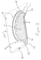
- Figure 2 is a partial cutaway, perspective view of the first embodiment of the baffle plate of Figure 1;
- Figure 3 is a partial cutaway, perspective view of a photoresist asher chamber assembly into which is incorporated a second embodiment of a baffle plate assembly constructed according to the present invention;
- Figure 4 is a partial cutaway, perspective view of a lower baffle plate of the second embodiment of the baffle plate assembly of Figure 3;
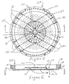
- Figure 5 is a plan view of the baffle plate assembly shown in Figure 3;
- Figure 6 is a sectional view of the baffle plate assembly of Figure 5, taken along the lines 6-6; and
- Figure 7 is a sectional view of the baffle plate assembly of Figure 6, taken along the lines 7-7.
- Referring now to the drawings, Figure 1 discloses a prior
art photoresist asher 10, comprising agas box 12; a microwaveplasma generator assembly 14; aprocess chamber 16 defining an interior cavity 17 in which is heated a semiconductor substrate such as awafer 18; and aradiant heater assembly 20 for heating thewafer 18, situated at the bottom of the process chamber. Atemperature probe 24, such as a thermocouple, is used to monitor the temperature of thewafer 18. Avacuum pump 26 is used to evacuate theprocess chamber 16 for processes requiring vacuum conditions. - A
monochromator 28 is used to monitor the optical emission characteristics of gases within the chamber to aid in process endpoint determination. Thewafer 18 is introduced into and removed from the process chamber via an appropriate load lock mechanism (not shown) via entry/exit passageway 30. Although the present invention is shown as being implemented within a photoresist asher, it may also be used in other semiconductor manufacturing equipment, such as residue removal and strip processes. - In operation, a desired mixture of gases is introduced into a
plasma tube 32 fromgas box 12 through aninlet conduit 34. Theplasma tube 32 is made of alumina (Al2O3) or sapphire to accommodate fluorine chemistries without etching or other degradation. The gases forming the desired mixture are stored in separate supplies (not shown) and mixed in thegas box 12 by means ofvalves 36 andpiping 38. One example of a desired gas mixture is forming gas (primarily nitrogen with a small percentage of hydrogen), and oxygen. A fluorine containing gas such as carbon tetrafluoride (CF4) may be added to the gas mixture to increase ashing rates for certain processes. - The desired gas mixture is energized by the microwave
plasma generator assembly 14 to form a reactive plasma that will ash photoresist on thewafer 18 in theprocess chamber 16 when heated by theradiant heater assembly 20. Amagnetron 40 generates microwave energy that is coupled to awaveguide 42. Microwave energy is fed from the waveguide through apertures (not shown) inmicrowave enclosure 44, which surrounds theplasma tube 32. - An outer
quartz cooling tube 46 surrounds theplasma tube 32, slightly separated therefrom. Pressurized air is fed into the gap between thetubes tube 32 during operation. Themicrowave enclosure 44 is segmented into sections shown byphantom lines 45. Segmentation of theenclosure 44 allows uniform microwave power distribution across the length of the alumina or sapphire plasma tube, and protects it from overheating by preventing an unacceptably large thermal gradient from developing along its axial length when suitable input power is provided. Each segment of theenclosure 44 is separately fed with microwave energy that passes through thequartz tube 46 and the alumina orsapphire tube 32 passing therethrough. - The gas mixture within the
plasma tube 32 is energized to create a plasma. Microwave traps 48 and 50 are provided at the ends of themicrowave enclosure 44 to prevent microwave leakage. Energized plasma (typically having a temperature of about 150° C) enters theprocess chamber 16 through anopening 51 in thetop wall 52 thereof. - Positioned between the
top wall 52 of theplasma chamber 16 and thewafer 18 being processed is a first preferred embodiment of the inventive gas distribution (or baffle)plate 54 of the present invention. Although shown as single member baffle plate, it is contemplated that the baffle plate may take the form of a dual-layered baffle plate assembly 154 (Figures 3-7) comprising upper and lower baffle plates. In either embodiment, the baffle plate 54 (Figures 1-2) and the baffle plate assembly 154 (Figures 3-7) evenly distribute the reactive plasma across the surface of thewafer 18 being processed, and provide means for cooling the gases within the plasma to achieve desired process results. - With reference back to Figure 1, in operation, the reactive plasma passes through the
baffle plate 54 and ashes the photoresist on thewafer 18. Theradiant heater assembly 20 comprises a plurality oftungsten halogen lamps 58 residing in areflector 56 that reflects and redirects the heat generated by the lamps toward the backside of thewafer 18 positioned within theprocess chamber 16 on quartz or ceramic pins 68. One or more temperature sensors 72, such as thermocouples, are mounted on the interior of processchamber side wall 53 to provide an indication of wall temperature. - The
baffle plate 54 shown in thephotoresist asher 10 of Figure 1 is shown in greater detail in Figure 2, which is designed for incorporation into a 200 millimieter (mm) wafer processing system. Thebaffle plate 54 comprises a generally planar gas distributioncentral portion 74, havingapertures 76 therein, surrounded by aflange 78. Theflange 78 surrounds the central portion and seats intermediate the processchamber side wall 53 and top wall 52 (see Figure 1).Seals 79 and 81, respectively, provide air tight connections between theflange 78 and theside wall 53, and between theflange 78 and thetop wall 52. Theseals 79 and 81 reside ingrooves 83 and 85, respectively, located in the flange 78 (see Figure 2). Theflange 78 also provides mountingholes 84 for mounting to thetop wall 52 andside wall 53. - The
central apertured portion 74 of thebaffle plate 54 is provided withinternal cooling passages 80 connected to coolingmedium inlet 82 and outlet 86. Thecooling passages 80 reduce the operating temperature of thebaffle plate 54, and extend about itscentral portion 74 in a configuration that avoids intersection with any of theapertures 76. In the preferrred embodiment, water is used as the cooling medium, although other liquids (e.g., oil) or gases (e.g., helium or nitrogen) having a high heat capacity are contemplated. As reactive gases pass through theapertures 76, the cooled baffle plate functions as a heat exchanger to remove heat from the reactive gases, thereby reducing its temperature. Thebaffle plate 54 also minimizes mobile ion contamination that can potentially cause wafer device damage, for example, weakening the dielectric strength of gate oxides. I - The baffle plate is preferably formed from a single piece of low-alloy anodized aluminum (e.g., Alcoa type C-276), which significantly improves the heat transfer characteristics of the baffle plate over known quartz baffle plates. The use of aluminum also permits the cooling passages to be drilled or machined directly therein. This makes the baffle plate less sensitive to inconsistencies in the reflector heating system and parasitic heating from the wafer, and allows for operation at a substantially uniform temperature.
- The use of aluminum also blocks a large percentage of ultraviolet (UV) energy emanating from the plasma tube that would otherwise make temperature control more difficult and possibly cause wafer device damage. Operating at a uniform surface temperature and minimizing exposure to UV radiation provides a substantial improvement in reaction rate uniformity across the surface of the wafer over known quartz baffle plates. In addition, maintaining a consistent baffle plate temperature eliminates the "first wafer effects" due to parasitic heating of the baffle plate as successive wafers are placed in the process chamber and heated to process temperature by the radiant heating system.
- Figure 3 shows a second embodiment of the invention, in which the baffle plate takes the form of the
baffle plate assembly 154, which is designed for incorporation into a 300 millimeter (mm) wafer processing system. Figure 3 is a partial cutaway, perspective view of a 300 mm photoresist asher chamber assembly 100 (shown without an associated radiant heater assembly) into which is incorporated thisbaffle plate assembly 154. Thebaffle plate assembly 154 comprises a generally planarupper baffle plate 155 andlower baffle plate 157 positioned generally parallel to each other and separated from one another. Theassembly 154 is shown attached to the 300mm process chamber 116. The upper andlower baffle plates apertures apertures 175 in the upper baffle plate are slightly larger than theapertures 176 in the lower baffle plate. A processchamber access port 128 is provided for either a vacuum pump or a monochromator. - In this second embodiment of the invention, both the
baffle plate assembly 154 and theprocess chamber 116 may be provided with active cooling mechanisms. With regard to the process chamber,internal cooling channels 156 are provided in theside walls 153 thereof. Coolingmedium inlets chamber side walls 153 are preferably formed from low-alloy anodized aluminum (e.g., Alcoa type C-276), which permits thecooling passages 156 to be drilled or machined directly therein, thereby making the side walls less sensitive to inconsistencies in the reflector heating system, and allowing for operation at a substantially uniform process temperature. - Although the
lower baffle plate 157 provided with active cooling, as explained further below, theupper baffle 155 plate is also not provided with an active cooling mechanism. Theupper baffle plate 155 is comprised merely of a solid, apertured quartz plate, attached to the lower plate by means ofposts 161 at attachment points 159 (see Figure 4 and 6). The upper baffle plate, which may be sapphire coated, functions to divert a portion of the hot gaseous plasma which does not pass through itsapertures 175 radially outward, so as to prevent the radially inward potion of thewafer 18 being processed from overheating and to promote reaction rate uniformity. A non-apertured sapphire plate 177 (Figures 5 and 6) covers the central portion of theupper baffle plate 155. - The active cooling mechanism provided by the
lower baffle plate 157 is more clearly shown in its partial cutaway, perspective view in Figure 4. Thelower baffle plate 157 comprises a generally planar gas distributioncentral portion 174, having theapertures 176 therein, surrounded by aflange 178. Theflange 178 provides the surface to which atop wall 181 of theprocess chamber 116 may be attached using mountingholes 184.Seal 179 provides an airtight connection between theflange 178 and the side wall 153 (Figure 3). Theseal 179 resides in agroove 183 in flange 178 (Figure 4). - The central
apertured portion 174 of thebaffle plate 157 is provided withinternal cooling passages 180 connected to coolingmedium inlet 182 and outlet 186 (Figure 3). As shown in Figures 4 and 6, thecooling passages 180 may extend from theflange 178 into and about thecentral portion 174 in a configuration that avoids intersection with any of theapertures 176. One preferred configuration is shown in Figure 7. - Still further, the cooling channels may also extend into the process chamber top wall. These individual cooling subsystems of these structural components (i.e., baffle plate, side walls and top wall) function to reduce the operating temperatures thereof. The cooling subsystems may either share a single gas or liquid coolant circulating system, or may be provided with independent circulating systems (gas or liquid) so as to provide independent temperature control and individual flow control thereof. Also, in embodiments of the invention wherein active cooling of the process chamber side walls and top wall are also provided, by maintaining these chamber surfaces at between 15° C - 30° C (just above the dew point), the wafer can remain sufficiently cool to prevent photoresist cracking during, for example, high-density ion implanted (HDII) wafer ash processes.
- The cooling passages minimize the spatial temperature gradient across the surface of the
lower baffle plate 157 and maintain the entire surface of the baffle plate at a uniform temperature. The cooling medium such as water (maintained, e.g., at 15° C - 80° C) flows into thechannels 180 viainlets 182 and flows out via outlets 186 (Figures 5 and 7), using a deionized water recirculating system including an air-cooled chiller assembly. The chiller assembly has a heat removal capacity greater than the heat generation rate of the process chamber even during rapid heating of the wafer. - Although water is used in the preferred embodiment as the cooling medium, other high heat capacity liquids or gases may be used, depending upon the required operating temperature of the lower baffle plate. For example, the lower baffle plate can be operated at up to 250° C to remove process residues from the surface of the plate. These residues may otherwise condense and remain on the surface of the lower plate if not periodically exposed to higher temperatures during wafer processing. At lower operating temperatures (e.g., 15° C - 80° C), as reactive gases pass through the
apertures 176, thelower baffle plate 157 functions as a heat exchanger to remove heat from the reactive gases, thereby reducing their temperature. - The
lower baffle plate 157 is preferably formed from a single piece of low-alloy anodized aluminum (e.g., Alcoa type C-276), which improves the heat transfer characteristics of the baffle plate over known quartz baffle plates. The use of aluminum also permits the cooling passages to be drilled or machined directly therein. This makes the baffle plate less sensitive to inconsistencies in the reflector heating system and parasitic heating from the wafer, and allows for operation at a substantially uniform temperature. - The use of aluminum also blocks a large percentage of ultraviolet (UV) energy emanating from the plasma tube that would otherwise make temperature control more difficult and possibly cause wafer device damage. Operating at a uniform surface temperature and minimizing exposure to UV radiation provides a substantial improvement in reaction rate uniformity across the surface of the wafer over known quartz baffle plates. In addition, maintaining a consistent baffle plate temperature eliminates the "first wafer effects" due to parasitic heating of the baffle plate as successive wafers are placed in the process chamber and heated to process temperature by the radiant heating system.
- A pressure drop across the
lower baffle plate 157 distributes the gas flow across the upper surface of the plate, in addition to increasing the heat transfer rate between the gas and the plate surfaces. This same effect, in combination with theupper quartz plate 155, reduces mobile ion contamination that can potentially cause device damage such as compromising the dielectric strength of gate oxides. The combination of the quartzupper plate 155 and the aluminumlower plate 157 in the dual-layeredbaffle plate assembly 154 has been found to be suitable for use in the corrosive conditions found in a process chamber used for photoresist removal, even when corrosive element-producing gases such as CF4 are utilized. - In operation, the systems 10 (200 mm) and 100 (300 mm) have been operated using the water-cooled
baffle plate 157 and thebaffle plate assembly 154, respectively, at maximum microwave power, under which conditions the gas temperatures have been reduced below the minimum expected process temperature, typically 80° C. Also, it has been possible to obtain a relatively flat temperature profile across the surface of the wafer during processing, resulting in reduced process non-uniformity due to the gas and radiation cooling effects of the cooled lower baffle plate. Active cooling of the lower baffle plate also reduces thermal loading of the baffle plate by the first-processed wafer to improve wafer-to-wafer process uniformity. - In one example, a 270° C ashing process was run while flowing water at 30° C through the
lower baffle plate 157 at a flow rate of .4 gallon per minute (gpm). An ash rate of 5.59 microns per minute was achieved with a 2.25% ash rate non-uniformity across the across the wafer. An ash rate of 5.66 microns per minute with a 6.2% ash rate non-uniformity across the wafer was obtained with a prior quartz non-actively cooled baffle blate. These test results show that using an actively-cooled baflle plate provides significant improvements in the area of process uniformity with minimal effect on ash rates. - Accordingly, a preferred embodiment of a method and system for cooling the reactive gases in a plasma processing system, as well as the wafer being processed, has been described. With the foregoing description in mind, however, it is understood that this description is made only by way of example, that the invention is not limited to the particular embodiments described herein, and that various rearrangements, modifications, and substitutions may be implemented with respect to the foregoing description without departing from the scope of the invention as defined by the following claims and their equivalents.
Claims (23)
- A plasma processing system (10) comprising:(i) a plasma generator (14);(ii) a processing chamber (16) having an interior processing cavity (17) in communication with said plasma generator (14) such that plasma within said generator may pass into said cavity and react with the surface of a substrate (18) residing therein; said processing chamber comprising walls (53) which at least partially define said cavity (17), said walls provided with first cooling passages (156) for reducing an operating temperature thereof ;(iii) a cooling medium inlet (158) and a cooling medium outlet (160) connected to said first cooling passages (156) to permit circulation of a cooling medium through said first cooling passages; and(iv) a radiant heater assembly (20) for heating the substrate (18).
- The plasma processing system (10) of claim 1, wherein said first cooling passages (156) are internal to said walls (53).
- The plasma processing system (10) of claim 2, wherein said walls (53) are comprised of low-alloy anodized aluminum and said first cooling passages (156) are machined into said walls.
- The plasma processing system (10) of claim 2, wherein said cooling medium is a liquid.
- The plasma processing system (10) of claim 4, wherein said cooling medium is water.
- The plasma processing system (10) of claim 2, wherein said cooling medium is a gas.
- The plasma processing system (10) of claim 6, wherein said cooling medium is helium or nitrogen.
- The plasma processing system (10) of claim 2, further comprising a baffle plate (54) positioned between said plasma generator (14) and said processing cavity (17), said baffle plate (54) having (i) apertures (76) therein for permitting the plasma to pass therethrough; (ii) second cooling passages (80) for accepting a flow of cooling medium to reduce an operating temperature of said baffle plate; and (iii) a cooling medium inlet (82) and a cooling medium outlet (86) connected to said second cooling passages (80) to permit circulation of a cooling medium therethrough.
- The plasma processing system (10) of claim 8, wherein said baffle plate (54) comprises a generally planar, apertured, gas distribution central portion (74) surrounded by a flange (78), said second cooling passages extending from said flange into said apertured central portion.
- The plasma processing system (10) of claim 8, wherein said first cooling passages (156) and said second cooling passages (80) are in communication with one another so as to permit them to share a single coolant circulating system.
- The plasma processing system (10) of claim 8, wherein said first cooling passages (156) and said second cooling passages (80) are not in communication with one another.
- The plasma processing system (10) of claim 11, wherein the cooling medium in said first cooling passages (156) is maintained approximately within the range of 15° C - 30° C, and the cooling medium in said second cooling passages (80) is maintained approximately within the range of 15° C - 80° C.
- The plasma processing system (10) of claim 8, wherein said baffle plate (54) is comprised of low-alloy anodized aluminum and said second cooling passages (80) are machined therein.
- A gas distribution plate (54) for a plasma processing system, comprising:(i) a generally planar central portion (74) having apertures (76) therein for permitting gas to pass therethrough;(ii) cooling passages (80) for accepting a flow of cooling medium to reduce an operating temperature of said baffle plate; and(iii) a cooling medium inlet (82) and a cooling medium outlet (86) connected to said second cooling passages (80) to permit circulation of a cooling medium therethrough.
- The gas distribution plate (54) of claim 14, wherein said central portion (74) is surrounded by a flange (78), said cooling passages (80) extending from said flange into said apertured central portion.
- The gas distribution plate (54) of claim 14, wherein said plate (54) is comprised of low-alloy anodized aluminum and said cooling passages (80) are machined therein.
- The gas distribution plate (54) of claim 14, wherein said cooling medium is a liquid.
- The gas distribution plate (54) of claim 17, wherein said cooling medium is water.
- The gas distribution plate (54) of claim 14, wherein said cooling medium is a gas.
- The gas distribution plate (54) of claim 19, wherein said cooling medium is helium or nitrogen.
- The gas distribution plate (54) of claim 14, further comprising a generally planar upper baffle plate (155) attached to said baffle plate (54) and separated by a distance therefrom, said upper baffle plate 155 provided with apertures 175.
- The gas distribution plate (54) of claim 21, wherein said apertures (175) in the upper baffle plate (155) are slightly larger than said apertures (176) in the lower baffle plate (54).
- The gas distribution plate (54) of claim 21, wherein said upper baffle plate (155) is comprised of quartz.
Applications Claiming Priority (2)
| Application Number | Priority Date | Filing Date | Title |
|---|---|---|---|
| US09/560,538 US6635117B1 (en) | 2000-04-26 | 2000-04-26 | Actively-cooled distribution plate for reducing reactive gas temperature in a plasma processing system |
| EP01303757A EP1150330B1 (en) | 2000-04-26 | 2001-04-25 | Actively-cooled distribution plate for reducing reactive gas temperature in a plasma processing system |
Related Parent Applications (2)
| Application Number | Title | Priority Date | Filing Date |
|---|---|---|---|
| EP01303757A Division EP1150330B1 (en) | 2000-04-26 | 2001-04-25 | Actively-cooled distribution plate for reducing reactive gas temperature in a plasma processing system |
| EP01303757.7 Division | 2001-04-25 |
Publications (3)
| Publication Number | Publication Date |
|---|---|
| EP1770753A2 true EP1770753A2 (en) | 2007-04-04 |
| EP1770753A3 EP1770753A3 (en) | 2008-02-20 |
| EP1770753B1 EP1770753B1 (en) | 2010-12-22 |
Family
ID=24238217
Family Applications (2)
| Application Number | Title | Priority Date | Filing Date |
|---|---|---|---|
| EP01303757A Expired - Lifetime EP1150330B1 (en) | 2000-04-26 | 2001-04-25 | Actively-cooled distribution plate for reducing reactive gas temperature in a plasma processing system |
| EP06022819A Expired - Lifetime EP1770753B1 (en) | 2000-04-26 | 2001-04-25 | Actively-cooled distribution plate for reducing reactive gas temperature in a plasma processing system |
Family Applications Before (1)
| Application Number | Title | Priority Date | Filing Date |
|---|---|---|---|
| EP01303757A Expired - Lifetime EP1150330B1 (en) | 2000-04-26 | 2001-04-25 | Actively-cooled distribution plate for reducing reactive gas temperature in a plasma processing system |
Country Status (6)
| Country | Link |
|---|---|
| US (2) | US6635117B1 (en) |
| EP (2) | EP1150330B1 (en) |
| JP (1) | JP4793528B2 (en) |
| KR (1) | KR100587628B1 (en) |
| DE (2) | DE60131695T2 (en) |
| TW (1) | TW490705B (en) |
Cited By (3)
| Publication number | Priority date | Publication date | Assignee | Title |
|---|---|---|---|---|
| WO2011149790A3 (en) * | 2010-05-27 | 2012-01-26 | Applied Materials, Inc. | Component temperature control by coolant flow control and heater duty cycle control |
| US9214315B2 (en) | 2010-01-29 | 2015-12-15 | Applied Materials, Inc. | Temperature control in plasma processing apparatus using pulsed heat transfer fluid flow |
| US10274270B2 (en) | 2011-10-27 | 2019-04-30 | Applied Materials, Inc. | Dual zone common catch heat exchanger/chiller |
Families Citing this family (501)
| Publication number | Priority date | Publication date | Assignee | Title |
|---|---|---|---|---|
| US6537419B1 (en) * | 2000-04-26 | 2003-03-25 | David W. Kinnard | Gas distribution plate assembly for providing laminar gas flow across the surface of a substrate |
| US6635117B1 (en) * | 2000-04-26 | 2003-10-21 | Axcelis Technologies, Inc. | Actively-cooled distribution plate for reducing reactive gas temperature in a plasma processing system |
| US6939434B2 (en) * | 2000-08-11 | 2005-09-06 | Applied Materials, Inc. | Externally excited torroidal plasma source with magnetic control of ion distribution |
| JP2002129334A (en) * | 2000-10-26 | 2002-05-09 | Applied Materials Inc | Cleaning method for vapor deposition apparatus and vapor deposition apparatus |
| KR100434487B1 (en) * | 2001-01-17 | 2004-06-05 | 삼성전자주식회사 | Shower head & film forming apparatus having the same |
| DE10134513A1 (en) * | 2001-07-16 | 2003-01-30 | Unaxis Balzers Ag | Lifting and support device |
| KR100476370B1 (en) * | 2002-07-19 | 2005-03-16 | 주식회사 하이닉스반도체 | Batch type Atomic Layer Deposition and method for insitu-cleaning in the batch type atomic layer deposition |
| US6945054B1 (en) | 2002-10-04 | 2005-09-20 | Richard S. Norman | Method and apparatus for cooling microelectronic complexes including multiple discrete functional modules |
| US20040235299A1 (en) * | 2003-05-22 | 2004-11-25 | Axcelis Technologies, Inc. | Plasma ashing apparatus and endpoint detection process |
| US8580076B2 (en) * | 2003-05-22 | 2013-11-12 | Lam Research Corporation | Plasma apparatus, gas distribution assembly for a plasma apparatus and processes therewith |
| US6976782B1 (en) | 2003-11-24 | 2005-12-20 | Lam Research Corporation | Methods and apparatus for in situ substrate temperature monitoring |
| US7892357B2 (en) * | 2004-01-12 | 2011-02-22 | Axcelis Technologies, Inc. | Gas distribution plate assembly for plasma reactors |
| US20050221618A1 (en) * | 2004-03-31 | 2005-10-06 | Amrhein Frederick J | System for controlling a plenum output flow geometry |
| US20050241767A1 (en) * | 2004-04-30 | 2005-11-03 | Ferris David S | Multi-piece baffle plate assembly for a plasma processing system |
| US20050250346A1 (en) * | 2004-05-06 | 2005-11-10 | Applied Materials, Inc. | Process and apparatus for post deposition treatment of low k dielectric materials |
| US7988816B2 (en) | 2004-06-21 | 2011-08-02 | Tokyo Electron Limited | Plasma processing apparatus and method |
| US7951262B2 (en) | 2004-06-21 | 2011-05-31 | Tokyo Electron Limited | Plasma processing apparatus and method |
| US20050284573A1 (en) * | 2004-06-24 | 2005-12-29 | Egley Fred D | Bare aluminum baffles for resist stripping chambers |
| US8349128B2 (en) | 2004-06-30 | 2013-01-08 | Applied Materials, Inc. | Method and apparatus for stable plasma processing |
| US20060000802A1 (en) * | 2004-06-30 | 2006-01-05 | Ajay Kumar | Method and apparatus for photomask plasma etching |
| CN102154628B (en) * | 2004-08-02 | 2014-05-07 | 维高仪器股份有限公司 | Multi-gas distribution injector for chemical vapor deposition reactors |
| US7449416B2 (en) | 2004-09-01 | 2008-11-11 | Axcelis Technologies, Inc. | Apparatus and plasma ashing process for increasing photoresist removal rate |
| JP2006080347A (en) * | 2004-09-10 | 2006-03-23 | Hitachi High-Technologies Corp | Plasma processing equipment |
| US20060228889A1 (en) * | 2005-03-31 | 2006-10-12 | Edelberg Erik A | Methods of removing resist from substrates in resist stripping chambers |
| US8298336B2 (en) * | 2005-04-01 | 2012-10-30 | Lam Research Corporation | High strip rate downstream chamber |
| US20060251827A1 (en) * | 2005-05-09 | 2006-11-09 | Applied Materials, Inc. | Tandem uv chamber for curing dielectric materials |
| US20060249175A1 (en) * | 2005-05-09 | 2006-11-09 | Applied Materials, Inc. | High efficiency UV curing system |
| JP4664119B2 (en) | 2005-05-17 | 2011-04-06 | 東京エレクトロン株式会社 | Plasma processing equipment |
| JP5044931B2 (en) * | 2005-10-31 | 2012-10-10 | 東京エレクトロン株式会社 | Gas supply apparatus and substrate processing apparatus |
| US20070119371A1 (en) * | 2005-11-04 | 2007-05-31 | Paul Ma | Apparatus and process for plasma-enhanced atomic layer deposition |
| KR100738873B1 (en) | 2006-02-07 | 2007-07-12 | 주식회사 에스에프에이 | Chemical Vapor Deposition Equipment for Flat Panel Displays |
| US7476291B2 (en) * | 2006-09-28 | 2009-01-13 | Lam Research Corporation | High chamber temperature process and chamber design for photo-resist stripping and post-metal etch passivation |
| US7909961B2 (en) * | 2006-10-30 | 2011-03-22 | Applied Materials, Inc. | Method and apparatus for photomask plasma etching |
| US7943005B2 (en) * | 2006-10-30 | 2011-05-17 | Applied Materials, Inc. | Method and apparatus for photomask plasma etching |
| KR100766440B1 (en) * | 2006-12-22 | 2007-10-15 | 엘지전자 주식회사 | Microwave Heater |
| WO2008114363A1 (en) * | 2007-03-16 | 2008-09-25 | Fujitsu Microelectronics Limited | Apparatus for producing semiconductor device and process for producing semiconductor device |
| JP2008243937A (en) | 2007-03-26 | 2008-10-09 | Tokyo Electron Ltd | Substrate processing apparatus and substrate processing method |
| US8500382B2 (en) * | 2007-05-22 | 2013-08-06 | Axcelis Technologies Inc. | Airflow management for particle abatement in semiconductor manufacturing equipment |
| US7651269B2 (en) * | 2007-07-19 | 2010-01-26 | Lam Research Corporation | Temperature probes having a thermally isolated tip |
| US8673080B2 (en) | 2007-10-16 | 2014-03-18 | Novellus Systems, Inc. | Temperature controlled showerhead |
| JP5230225B2 (en) * | 2008-03-06 | 2013-07-10 | 東京エレクトロン株式会社 | Lid parts, processing gas diffusion supply device, and substrate processing device |
| US8252114B2 (en) * | 2008-03-28 | 2012-08-28 | Tokyo Electron Limited | Gas distribution system and method for distributing process gas in a processing system |
| US20100206229A1 (en) * | 2008-05-30 | 2010-08-19 | Alta Devices, Inc. | Vapor deposition reactor system |
| US20100212591A1 (en) * | 2008-05-30 | 2010-08-26 | Alta Devices, Inc. | Reactor lid assembly for vapor deposition |
| US8679288B2 (en) | 2008-06-09 | 2014-03-25 | Lam Research Corporation | Showerhead electrode assemblies for plasma processing apparatuses |
| JP5661622B2 (en) * | 2008-07-07 | 2015-01-28 | ラム リサーチ コーポレーションLam Research Corporation | Plasma facing probe apparatus with a vacuum gap for use in a plasma processing chamber |
| US8179152B2 (en) | 2008-07-07 | 2012-05-15 | Lam Research Corporation | Passive capacitively-coupled electrostatic (CCE) probe arrangement for detecting plasma instabilities in a plasma processing chamber |
| JP5231117B2 (en) * | 2008-07-24 | 2013-07-10 | 株式会社ニューフレアテクノロジー | Film forming apparatus and film forming method |
| EP2151509A1 (en) * | 2008-08-04 | 2010-02-10 | Applied Materials, Inc. | Reactive gas distributor, reactive gas treatment system, and reactive gas treatment method |
| US8449679B2 (en) | 2008-08-15 | 2013-05-28 | Lam Research Corporation | Temperature controlled hot edge ring assembly |
| US10378106B2 (en) | 2008-11-14 | 2019-08-13 | Asm Ip Holding B.V. | Method of forming insulation film by modified PEALD |
| KR101037188B1 (en) | 2008-12-17 | 2011-05-26 | 세메스 주식회사 | Plasma processing equipment |
| JP5479867B2 (en) | 2009-01-14 | 2014-04-23 | 東京エレクトロン株式会社 | Inductively coupled plasma processing equipment |
| TW201042075A (en) * | 2009-03-16 | 2010-12-01 | Alta Devices Inc | Showerhead for vapor deposition |
| US9394608B2 (en) | 2009-04-06 | 2016-07-19 | Asm America, Inc. | Semiconductor processing reactor and components thereof |
| KR101110080B1 (en) * | 2009-07-08 | 2012-03-13 | 주식회사 유진테크 | Substrate treatment method for selectively inserting diffusion plate |
| US8802201B2 (en) | 2009-08-14 | 2014-08-12 | Asm America, Inc. | Systems and methods for thin-film deposition of metal oxides using excited nitrogen-oxygen species |
| US9338871B2 (en) | 2010-01-29 | 2016-05-10 | Applied Materials, Inc. | Feedforward temperature control for plasma processing apparatus |
| JP5903429B2 (en) | 2010-04-30 | 2016-04-13 | アプライド マテリアルズ インコーポレイテッドApplied Materials,Incorporated | Vertical in-line CVD system |
| JP5373702B2 (en) * | 2010-06-07 | 2013-12-18 | 株式会社Sen | Ion beam scan processing apparatus and ion beam scan processing method |
| US8845806B2 (en) * | 2010-10-22 | 2014-09-30 | Asm Japan K.K. | Shower plate having different aperture dimensions and/or distributions |
| US9070760B2 (en) * | 2011-03-14 | 2015-06-30 | Plasma-Therm Llc | Method and apparatus for plasma dicing a semi-conductor wafer |
| US9129778B2 (en) | 2011-03-18 | 2015-09-08 | Lam Research Corporation | Fluid distribution members and/or assemblies |
| US8562785B2 (en) * | 2011-05-31 | 2013-10-22 | Lam Research Corporation | Gas distribution showerhead for inductively coupled plasma etch reactor |
| US9245717B2 (en) | 2011-05-31 | 2016-01-26 | Lam Research Corporation | Gas distribution system for ceramic showerhead of plasma etch reactor |
| US9312155B2 (en) | 2011-06-06 | 2016-04-12 | Asm Japan K.K. | High-throughput semiconductor-processing apparatus equipped with multiple dual-chamber modules |
| US20120315396A1 (en) * | 2011-06-13 | 2012-12-13 | Intermolecular, Inc. | Apparatus and method for combinatorial plasma distribution through a multi-zoned showerhead |
| US9793148B2 (en) | 2011-06-22 | 2017-10-17 | Asm Japan K.K. | Method for positioning wafers in multiple wafer transport |
| US10364496B2 (en) | 2011-06-27 | 2019-07-30 | Asm Ip Holding B.V. | Dual section module having shared and unshared mass flow controllers |
| USD664249S1 (en) * | 2011-07-01 | 2012-07-24 | Applied Materials, Inc. | Flow blocker plate |
| US10854498B2 (en) | 2011-07-15 | 2020-12-01 | Asm Ip Holding B.V. | Wafer-supporting device and method for producing same |
| US20130023129A1 (en) | 2011-07-20 | 2013-01-24 | Asm America, Inc. | Pressure transmitter for a semiconductor processing environment |
| JP1438745S (en) * | 2011-09-20 | 2015-04-06 | ||
| JP1438319S (en) | 2011-09-20 | 2015-04-06 | ||
| US9017481B1 (en) | 2011-10-28 | 2015-04-28 | Asm America, Inc. | Process feed management for semiconductor substrate processing |
| US8946830B2 (en) | 2012-04-04 | 2015-02-03 | Asm Ip Holdings B.V. | Metal oxide protective layer for a semiconductor device |
| US9447499B2 (en) | 2012-06-22 | 2016-09-20 | Novellus Systems, Inc. | Dual plenum, axi-symmetric showerhead with edge-to-center gas delivery |
| US8875728B2 (en) * | 2012-07-12 | 2014-11-04 | Siliken Chemicals, S.L. | Cooled gas distribution plate, thermal bridge breaking system, and related methods |
| US9558931B2 (en) | 2012-07-27 | 2017-01-31 | Asm Ip Holding B.V. | System and method for gas-phase sulfur passivation of a semiconductor surface |
| JP6172660B2 (en) * | 2012-08-23 | 2017-08-02 | 東京エレクトロン株式会社 | Film forming apparatus and method for forming low dielectric constant film |
| US9659799B2 (en) | 2012-08-28 | 2017-05-23 | Asm Ip Holding B.V. | Systems and methods for dynamic semiconductor process scheduling |
| US9021985B2 (en) | 2012-09-12 | 2015-05-05 | Asm Ip Holdings B.V. | Process gas management for an inductively-coupled plasma deposition reactor |
| KR20140038070A (en) * | 2012-09-20 | 2014-03-28 | 삼성코닝정밀소재 주식회사 | Gas injector and injector pipe thereof |
| US9324811B2 (en) | 2012-09-26 | 2016-04-26 | Asm Ip Holding B.V. | Structures and devices including a tensile-stressed silicon arsenic layer and methods of forming same |
| US10714315B2 (en) | 2012-10-12 | 2020-07-14 | Asm Ip Holdings B.V. | Semiconductor reaction chamber showerhead |
| JP6096470B2 (en) * | 2012-10-29 | 2017-03-15 | 東京エレクトロン株式会社 | Plasma processing method and plasma processing apparatus |
| US10316409B2 (en) * | 2012-12-21 | 2019-06-11 | Novellus Systems, Inc. | Radical source design for remote plasma atomic layer deposition |
| US9640416B2 (en) | 2012-12-26 | 2017-05-02 | Asm Ip Holding B.V. | Single-and dual-chamber module-attachable wafer-handling chamber |
| US20160376700A1 (en) | 2013-02-01 | 2016-12-29 | Asm Ip Holding B.V. | System for treatment of deposition reactor |
| US20140235069A1 (en) * | 2013-02-15 | 2014-08-21 | Novellus Systems, Inc. | Multi-plenum showerhead with temperature control |
| US9748121B2 (en) * | 2013-03-05 | 2017-08-29 | Applied Materials, Inc. | Thermal coupled quartz dome heat sink |
| US9589770B2 (en) | 2013-03-08 | 2017-03-07 | Asm Ip Holding B.V. | Method and systems for in-situ formation of intermediate reactive species |
| US9484191B2 (en) | 2013-03-08 | 2016-11-01 | Asm Ip Holding B.V. | Pulsed remote plasma method and system |
| US9322097B2 (en) | 2013-03-13 | 2016-04-26 | Applied Materials, Inc. | EPI base ring |
| CN103276371B (en) * | 2013-03-26 | 2015-12-09 | 中晟光电设备(上海)有限公司 | The diffuser of CVD equipment, refrigerating unit and method of cooling |
| US9677176B2 (en) | 2013-07-03 | 2017-06-13 | Novellus Systems, Inc. | Multi-plenum, dual-temperature showerhead |
| US8993054B2 (en) | 2013-07-12 | 2015-03-31 | Asm Ip Holding B.V. | Method and system to reduce outgassing in a reaction chamber |
| US9859145B2 (en) * | 2013-07-17 | 2018-01-02 | Lam Research Corporation | Cooled pin lifter paddle for semiconductor substrate processing apparatus |
| US9018111B2 (en) | 2013-07-22 | 2015-04-28 | Asm Ip Holding B.V. | Semiconductor reaction chamber with plasma capabilities |
| US9793115B2 (en) | 2013-08-14 | 2017-10-17 | Asm Ip Holding B.V. | Structures and devices including germanium-tin films and methods of forming same |
| US9240412B2 (en) | 2013-09-27 | 2016-01-19 | Asm Ip Holding B.V. | Semiconductor structure and device and methods of forming same using selective epitaxial process |
| US9556516B2 (en) | 2013-10-09 | 2017-01-31 | ASM IP Holding B.V | Method for forming Ti-containing film by PEALD using TDMAT or TDEAT |
| US10179947B2 (en) | 2013-11-26 | 2019-01-15 | Asm Ip Holding B.V. | Method for forming conformal nitrided, oxidized, or carbonized dielectric film by atomic layer deposition |
| US10683571B2 (en) | 2014-02-25 | 2020-06-16 | Asm Ip Holding B.V. | Gas supply manifold and method of supplying gases to chamber using same |
| US9447498B2 (en) | 2014-03-18 | 2016-09-20 | Asm Ip Holding B.V. | Method for performing uniform processing in gas system-sharing multiple reaction chambers |
| US10167557B2 (en) | 2014-03-18 | 2019-01-01 | Asm Ip Holding B.V. | Gas distribution system, reactor including the system, and methods of using the same |
| US11015245B2 (en) | 2014-03-19 | 2021-05-25 | Asm Ip Holding B.V. | Gas-phase reactor and system having exhaust plenum and components thereof |
| US9404587B2 (en) | 2014-04-24 | 2016-08-02 | ASM IP Holding B.V | Lockout tagout for semiconductor vacuum valve |
| US10741365B2 (en) * | 2014-05-05 | 2020-08-11 | Lam Research Corporation | Low volume showerhead with porous baffle |
| US10858737B2 (en) | 2014-07-28 | 2020-12-08 | Asm Ip Holding B.V. | Showerhead assembly and components thereof |
| US9543180B2 (en) | 2014-08-01 | 2017-01-10 | Asm Ip Holding B.V. | Apparatus and method for transporting wafers between wafer carrier and process tool under vacuum |
| US9890456B2 (en) | 2014-08-21 | 2018-02-13 | Asm Ip Holding B.V. | Method and system for in situ formation of gas-phase compounds |
| KR101568363B1 (en) | 2014-08-27 | 2015-11-12 | 피에스케이 주식회사 | Substrate treating apparatus and baffle |
| US9657845B2 (en) | 2014-10-07 | 2017-05-23 | Asm Ip Holding B.V. | Variable conductance gas distribution apparatus and method |
| US10941490B2 (en) | 2014-10-07 | 2021-03-09 | Asm Ip Holding B.V. | Multiple temperature range susceptor, assembly, reactor and system including the susceptor, and methods of using the same |
| KR102300403B1 (en) | 2014-11-19 | 2021-09-09 | 에이에스엠 아이피 홀딩 비.브이. | Method of depositing thin film |
| KR102263121B1 (en) | 2014-12-22 | 2021-06-09 | 에이에스엠 아이피 홀딩 비.브이. | Semiconductor device and manufacuring method thereof |
| US9478415B2 (en) | 2015-02-13 | 2016-10-25 | Asm Ip Holding B.V. | Method for forming film having low resistance and shallow junction depth |
| US10529542B2 (en) | 2015-03-11 | 2020-01-07 | Asm Ip Holdings B.V. | Cross-flow reactor and method |
| US10276355B2 (en) | 2015-03-12 | 2019-04-30 | Asm Ip Holding B.V. | Multi-zone reactor, system including the reactor, and method of using the same |
| US10378107B2 (en) * | 2015-05-22 | 2019-08-13 | Lam Research Corporation | Low volume showerhead with faceplate holes for improved flow uniformity |
| US10023959B2 (en) | 2015-05-26 | 2018-07-17 | Lam Research Corporation | Anti-transient showerhead |
| US10458018B2 (en) | 2015-06-26 | 2019-10-29 | Asm Ip Holding B.V. | Structures including metal carbide material, devices including the structures, and methods of forming same |
| US10600673B2 (en) | 2015-07-07 | 2020-03-24 | Asm Ip Holding B.V. | Magnetic susceptor to baseplate seal |
| US9899291B2 (en) | 2015-07-13 | 2018-02-20 | Asm Ip Holding B.V. | Method for protecting layer by forming hydrocarbon-based extremely thin film |
| US10043661B2 (en) | 2015-07-13 | 2018-08-07 | Asm Ip Holding B.V. | Method for protecting layer by forming hydrocarbon-based extremely thin film |
| CN106356318B (en) * | 2015-07-16 | 2019-10-18 | 中微半导体设备(上海)股份有限公司 | A kind of gas distribution diffusion plate, plasma processor |
| US10083836B2 (en) | 2015-07-24 | 2018-09-25 | Asm Ip Holding B.V. | Formation of boron-doped titanium metal films with high work function |
| US10087525B2 (en) | 2015-08-04 | 2018-10-02 | Asm Ip Holding B.V. | Variable gap hard stop design |
| US9647114B2 (en) | 2015-08-14 | 2017-05-09 | Asm Ip Holding B.V. | Methods of forming highly p-type doped germanium tin films and structures and devices including the films |
| US9711345B2 (en) | 2015-08-25 | 2017-07-18 | Asm Ip Holding B.V. | Method for forming aluminum nitride-based film by PEALD |
| US9960072B2 (en) | 2015-09-29 | 2018-05-01 | Asm Ip Holding B.V. | Variable adjustment for precise matching of multiple chamber cavity housings |
| US9909214B2 (en) | 2015-10-15 | 2018-03-06 | Asm Ip Holding B.V. | Method for depositing dielectric film in trenches by PEALD |
| US9899210B2 (en) * | 2015-10-20 | 2018-02-20 | Taiwan Semiconductor Manufacturing Co., Ltd. | Chemical vapor deposition apparatus and method for manufacturing semiconductor device using the same |
| US10211308B2 (en) | 2015-10-21 | 2019-02-19 | Asm Ip Holding B.V. | NbMC layers |
| US10322384B2 (en) | 2015-11-09 | 2019-06-18 | Asm Ip Holding B.V. | Counter flow mixer for process chamber |
| US9455138B1 (en) | 2015-11-10 | 2016-09-27 | Asm Ip Holding B.V. | Method for forming dielectric film in trenches by PEALD using H-containing gas |
| US9905420B2 (en) | 2015-12-01 | 2018-02-27 | Asm Ip Holding B.V. | Methods of forming silicon germanium tin films and structures and devices including the films |
| US9607837B1 (en) | 2015-12-21 | 2017-03-28 | Asm Ip Holding B.V. | Method for forming silicon oxide cap layer for solid state diffusion process |
| US9627221B1 (en) | 2015-12-28 | 2017-04-18 | Asm Ip Holding B.V. | Continuous process incorporating atomic layer etching |
| US9735024B2 (en) | 2015-12-28 | 2017-08-15 | Asm Ip Holding B.V. | Method of atomic layer etching using functional group-containing fluorocarbon |
| US11139308B2 (en) | 2015-12-29 | 2021-10-05 | Asm Ip Holding B.V. | Atomic layer deposition of III-V compounds to form V-NAND devices |
| US9754779B1 (en) | 2016-02-19 | 2017-09-05 | Asm Ip Holding B.V. | Method for forming silicon nitride film selectively on sidewalls or flat surfaces of trenches |
| US10468251B2 (en) | 2016-02-19 | 2019-11-05 | Asm Ip Holding B.V. | Method for forming spacers using silicon nitride film for spacer-defined multiple patterning |
| US10529554B2 (en) | 2016-02-19 | 2020-01-07 | Asm Ip Holding B.V. | Method for forming silicon nitride film selectively on sidewalls or flat surfaces of trenches |
| US10501866B2 (en) | 2016-03-09 | 2019-12-10 | Asm Ip Holding B.V. | Gas distribution apparatus for improved film uniformity in an epitaxial system |
| US10343920B2 (en) | 2016-03-18 | 2019-07-09 | Asm Ip Holding B.V. | Aligned carbon nanotubes |
| US9892913B2 (en) | 2016-03-24 | 2018-02-13 | Asm Ip Holding B.V. | Radial and thickness control via biased multi-port injection settings |
| US10190213B2 (en) | 2016-04-21 | 2019-01-29 | Asm Ip Holding B.V. | Deposition of metal borides |
| US10865475B2 (en) | 2016-04-21 | 2020-12-15 | Asm Ip Holding B.V. | Deposition of metal borides and silicides |
| US10087522B2 (en) | 2016-04-21 | 2018-10-02 | Asm Ip Holding B.V. | Deposition of metal borides |
| US10032628B2 (en) | 2016-05-02 | 2018-07-24 | Asm Ip Holding B.V. | Source/drain performance through conformal solid state doping |
| US10367080B2 (en) | 2016-05-02 | 2019-07-30 | Asm Ip Holding B.V. | Method of forming a germanium oxynitride film |
| KR102592471B1 (en) | 2016-05-17 | 2023-10-20 | 에이에스엠 아이피 홀딩 비.브이. | Method of forming metal interconnection and method of fabricating semiconductor device using the same |
| US11453943B2 (en) | 2016-05-25 | 2022-09-27 | Asm Ip Holding B.V. | Method for forming carbon-containing silicon/metal oxide or nitride film by ALD using silicon precursor and hydrocarbon precursor |
| US10388509B2 (en) | 2016-06-28 | 2019-08-20 | Asm Ip Holding B.V. | Formation of epitaxial layers via dislocation filtering |
| US9859151B1 (en) | 2016-07-08 | 2018-01-02 | Asm Ip Holding B.V. | Selective film deposition method to form air gaps |
| US10612137B2 (en) | 2016-07-08 | 2020-04-07 | Asm Ip Holdings B.V. | Organic reactants for atomic layer deposition |
| US9793135B1 (en) | 2016-07-14 | 2017-10-17 | ASM IP Holding B.V | Method of cyclic dry etching using etchant film |
| US10714385B2 (en) | 2016-07-19 | 2020-07-14 | Asm Ip Holding B.V. | Selective deposition of tungsten |
| KR102354490B1 (en) | 2016-07-27 | 2022-01-21 | 에이에스엠 아이피 홀딩 비.브이. | Method of processing a substrate |
| KR102532607B1 (en) | 2016-07-28 | 2023-05-15 | 에이에스엠 아이피 홀딩 비.브이. | Substrate processing apparatus and method of operating the same |
| US9887082B1 (en) | 2016-07-28 | 2018-02-06 | Asm Ip Holding B.V. | Method and apparatus for filling a gap |
| US9812320B1 (en) | 2016-07-28 | 2017-11-07 | Asm Ip Holding B.V. | Method and apparatus for filling a gap |
| US10177025B2 (en) | 2016-07-28 | 2019-01-08 | Asm Ip Holding B.V. | Method and apparatus for filling a gap |
| US10395919B2 (en) | 2016-07-28 | 2019-08-27 | Asm Ip Holding B.V. | Method and apparatus for filling a gap |
| US10090316B2 (en) | 2016-09-01 | 2018-10-02 | Asm Ip Holding B.V. | 3D stacked multilayer semiconductor memory using doped select transistor channel |
| US10410943B2 (en) | 2016-10-13 | 2019-09-10 | Asm Ip Holding B.V. | Method for passivating a surface of a semiconductor and related systems |
| US10643826B2 (en) | 2016-10-26 | 2020-05-05 | Asm Ip Holdings B.V. | Methods for thermally calibrating reaction chambers |
| US11532757B2 (en) | 2016-10-27 | 2022-12-20 | Asm Ip Holding B.V. | Deposition of charge trapping layers |
| US10714350B2 (en) | 2016-11-01 | 2020-07-14 | ASM IP Holdings, B.V. | Methods for forming a transition metal niobium nitride film on a substrate by atomic layer deposition and related semiconductor device structures |
| US10229833B2 (en) | 2016-11-01 | 2019-03-12 | Asm Ip Holding B.V. | Methods for forming a transition metal nitride film on a substrate by atomic layer deposition and related semiconductor device structures |
| US10643904B2 (en) | 2016-11-01 | 2020-05-05 | Asm Ip Holdings B.V. | Methods for forming a semiconductor device and related semiconductor device structures |
| US10435790B2 (en) | 2016-11-01 | 2019-10-08 | Asm Ip Holding B.V. | Method of subatmospheric plasma-enhanced ALD using capacitively coupled electrodes with narrow gap |
| US10134757B2 (en) | 2016-11-07 | 2018-11-20 | Asm Ip Holding B.V. | Method of processing a substrate and a device manufactured by using the method |
| KR102546317B1 (en) | 2016-11-15 | 2023-06-21 | 에이에스엠 아이피 홀딩 비.브이. | Gas supply unit and substrate processing apparatus including the same |
| US10340135B2 (en) | 2016-11-28 | 2019-07-02 | Asm Ip Holding B.V. | Method of topologically restricted plasma-enhanced cyclic deposition of silicon or metal nitride |
| US10604841B2 (en) | 2016-12-14 | 2020-03-31 | Lam Research Corporation | Integrated showerhead with thermal control for delivering radical and precursor gas to a downstream chamber to enable remote plasma film deposition |
| KR102762543B1 (en) | 2016-12-14 | 2025-02-05 | 에이에스엠 아이피 홀딩 비.브이. | Substrate processing apparatus |
| US11447861B2 (en) | 2016-12-15 | 2022-09-20 | Asm Ip Holding B.V. | Sequential infiltration synthesis apparatus and a method of forming a patterned structure |
| US11581186B2 (en) | 2016-12-15 | 2023-02-14 | Asm Ip Holding B.V. | Sequential infiltration synthesis apparatus |
| US9916980B1 (en) | 2016-12-15 | 2018-03-13 | Asm Ip Holding B.V. | Method of forming a structure on a substrate |
| KR102700194B1 (en) | 2016-12-19 | 2024-08-28 | 에이에스엠 아이피 홀딩 비.브이. | Substrate processing apparatus |
| US10269558B2 (en) | 2016-12-22 | 2019-04-23 | Asm Ip Holding B.V. | Method of forming a structure on a substrate |
| US10867788B2 (en) | 2016-12-28 | 2020-12-15 | Asm Ip Holding B.V. | Method of forming a structure on a substrate |
| US11390950B2 (en) | 2017-01-10 | 2022-07-19 | Asm Ip Holding B.V. | Reactor system and method to reduce residue buildup during a film deposition process |
| US10655221B2 (en) | 2017-02-09 | 2020-05-19 | Asm Ip Holding B.V. | Method for depositing oxide film by thermal ALD and PEALD |
| US10468261B2 (en) | 2017-02-15 | 2019-11-05 | Asm Ip Holding B.V. | Methods for forming a metallic film on a substrate by cyclical deposition and related semiconductor device structures |
| US10283353B2 (en) | 2017-03-29 | 2019-05-07 | Asm Ip Holding B.V. | Method of reforming insulating film deposited on substrate with recess pattern |
| US10529563B2 (en) | 2017-03-29 | 2020-01-07 | Asm Ip Holdings B.V. | Method for forming doped metal oxide films on a substrate by cyclical deposition and related semiconductor device structures |
| US10103040B1 (en) | 2017-03-31 | 2018-10-16 | Asm Ip Holding B.V. | Apparatus and method for manufacturing a semiconductor device |
| USD830981S1 (en) | 2017-04-07 | 2018-10-16 | Asm Ip Holding B.V. | Susceptor for semiconductor substrate processing apparatus |
| KR102457289B1 (en) | 2017-04-25 | 2022-10-21 | 에이에스엠 아이피 홀딩 비.브이. | Method for depositing a thin film and manufacturing a semiconductor device |
| US10770286B2 (en) | 2017-05-08 | 2020-09-08 | Asm Ip Holdings B.V. | Methods for selectively forming a silicon nitride film on a substrate and related semiconductor device structures |
| US10446393B2 (en) | 2017-05-08 | 2019-10-15 | Asm Ip Holding B.V. | Methods for forming silicon-containing epitaxial layers and related semiconductor device structures |
| US10892156B2 (en) | 2017-05-08 | 2021-01-12 | Asm Ip Holding B.V. | Methods for forming a silicon nitride film on a substrate and related semiconductor device structures |
| US10504742B2 (en) | 2017-05-31 | 2019-12-10 | Asm Ip Holding B.V. | Method of atomic layer etching using hydrogen plasma |
| US10886123B2 (en) | 2017-06-02 | 2021-01-05 | Asm Ip Holding B.V. | Methods for forming low temperature semiconductor layers and related semiconductor device structures |
| US10790119B2 (en) | 2017-06-09 | 2020-09-29 | Mattson Technology, Inc | Plasma processing apparatus with post plasma gas injection |
| US11201036B2 (en) * | 2017-06-09 | 2021-12-14 | Beijing E-Town Semiconductor Technology Co., Ltd | Plasma strip tool with uniformity control |
| US12040200B2 (en) | 2017-06-20 | 2024-07-16 | Asm Ip Holding B.V. | Semiconductor processing apparatus and methods for calibrating a semiconductor processing apparatus |
| US11306395B2 (en) | 2017-06-28 | 2022-04-19 | Asm Ip Holding B.V. | Methods for depositing a transition metal nitride film on a substrate by atomic layer deposition and related deposition apparatus |
| US10685834B2 (en) | 2017-07-05 | 2020-06-16 | Asm Ip Holdings B.V. | Methods for forming a silicon germanium tin layer and related semiconductor device structures |
| KR20190009245A (en) | 2017-07-18 | 2019-01-28 | 에이에스엠 아이피 홀딩 비.브이. | Methods for forming a semiconductor device structure and related semiconductor device structures |
| US11374112B2 (en) | 2017-07-19 | 2022-06-28 | Asm Ip Holding B.V. | Method for depositing a group IV semiconductor and related semiconductor device structures |
| US11018002B2 (en) | 2017-07-19 | 2021-05-25 | Asm Ip Holding B.V. | Method for selectively depositing a Group IV semiconductor and related semiconductor device structures |
| US10541333B2 (en) | 2017-07-19 | 2020-01-21 | Asm Ip Holding B.V. | Method for depositing a group IV semiconductor and related semiconductor device structures |
| US10312055B2 (en) | 2017-07-26 | 2019-06-04 | Asm Ip Holding B.V. | Method of depositing film by PEALD using negative bias |
| US10605530B2 (en) | 2017-07-26 | 2020-03-31 | Asm Ip Holding B.V. | Assembly of a liner and a flange for a vertical furnace as well as the liner and the vertical furnace |
| US10590535B2 (en) | 2017-07-26 | 2020-03-17 | Asm Ip Holdings B.V. | Chemical treatment, deposition and/or infiltration apparatus and method for using the same |
| TWI815813B (en) | 2017-08-04 | 2023-09-21 | 荷蘭商Asm智慧財產控股公司 | Showerhead assembly for distributing a gas within a reaction chamber |
| US10770336B2 (en) | 2017-08-08 | 2020-09-08 | Asm Ip Holding B.V. | Substrate lift mechanism and reactor including same |
| US10692741B2 (en) | 2017-08-08 | 2020-06-23 | Asm Ip Holdings B.V. | Radiation shield |
| US11769682B2 (en) | 2017-08-09 | 2023-09-26 | Asm Ip Holding B.V. | Storage apparatus for storing cassettes for substrates and processing apparatus equipped therewith |
| US11139191B2 (en) | 2017-08-09 | 2021-10-05 | Asm Ip Holding B.V. | Storage apparatus for storing cassettes for substrates and processing apparatus equipped therewith |
| US10249524B2 (en) | 2017-08-09 | 2019-04-02 | Asm Ip Holding B.V. | Cassette holder assembly for a substrate cassette and holding member for use in such assembly |
| US10236177B1 (en) | 2017-08-22 | 2019-03-19 | ASM IP Holding B.V.. | Methods for depositing a doped germanium tin semiconductor and related semiconductor device structures |
| USD900036S1 (en) | 2017-08-24 | 2020-10-27 | Asm Ip Holding B.V. | Heater electrical connector and adapter |
| US11830730B2 (en) | 2017-08-29 | 2023-11-28 | Asm Ip Holding B.V. | Layer forming method and apparatus |
| US11295980B2 (en) | 2017-08-30 | 2022-04-05 | Asm Ip Holding B.V. | Methods for depositing a molybdenum metal film over a dielectric surface of a substrate by a cyclical deposition process and related semiconductor device structures |
| US11056344B2 (en) | 2017-08-30 | 2021-07-06 | Asm Ip Holding B.V. | Layer forming method |
| KR102491945B1 (en) | 2017-08-30 | 2023-01-26 | 에이에스엠 아이피 홀딩 비.브이. | Substrate processing apparatus |
| KR102401446B1 (en) | 2017-08-31 | 2022-05-24 | 에이에스엠 아이피 홀딩 비.브이. | Substrate processing apparatus |
| DE202017105481U1 (en) * | 2017-09-11 | 2018-12-12 | Aixtron Se | Gas inlet member for a CVD or PVD reactor |
| US10607895B2 (en) | 2017-09-18 | 2020-03-31 | Asm Ip Holdings B.V. | Method for forming a semiconductor device structure comprising a gate fill metal |
| KR102630301B1 (en) | 2017-09-21 | 2024-01-29 | 에이에스엠 아이피 홀딩 비.브이. | Method of sequential infiltration synthesis treatment of infiltrateable material and structures and devices formed using same |
| US10844484B2 (en) | 2017-09-22 | 2020-11-24 | Asm Ip Holding B.V. | Apparatus for dispensing a vapor phase reactant to a reaction chamber and related methods |
| US10658205B2 (en) | 2017-09-28 | 2020-05-19 | Asm Ip Holdings B.V. | Chemical dispensing apparatus and methods for dispensing a chemical to a reaction chamber |
| US10403504B2 (en) | 2017-10-05 | 2019-09-03 | Asm Ip Holding B.V. | Method for selectively depositing a metallic film on a substrate |
| US10319588B2 (en) | 2017-10-10 | 2019-06-11 | Asm Ip Holding B.V. | Method for depositing a metal chalcogenide on a substrate by cyclical deposition |
| US10923344B2 (en) | 2017-10-30 | 2021-02-16 | Asm Ip Holding B.V. | Methods for forming a semiconductor structure and related semiconductor structures |
| KR102443047B1 (en) | 2017-11-16 | 2022-09-14 | 에이에스엠 아이피 홀딩 비.브이. | Substrate processing apparatus method and apparatus manufactured thereby |
| US10910262B2 (en) | 2017-11-16 | 2021-02-02 | Asm Ip Holding B.V. | Method of selectively depositing a capping layer structure on a semiconductor device structure |
| US11022879B2 (en) | 2017-11-24 | 2021-06-01 | Asm Ip Holding B.V. | Method of forming an enhanced unexposed photoresist layer |
| JP7206265B2 (en) | 2017-11-27 | 2023-01-17 | エーエスエム アイピー ホールディング ビー.ブイ. | Equipment with a clean mini-environment |
| CN111316417B (en) | 2017-11-27 | 2023-12-22 | 阿斯莫Ip控股公司 | Storage device for use with batch furnaces for storing wafer cassettes |
| US10290508B1 (en) | 2017-12-05 | 2019-05-14 | Asm Ip Holding B.V. | Method for forming vertical spacers for spacer-defined patterning |
| JP7546483B2 (en) | 2017-12-08 | 2024-09-06 | ラム リサーチ コーポレーション | Integrated showerhead with improved hole pattern for delivering radical and precursor gases to a downstream chamber to enable remote plasma film deposition |
| US10872771B2 (en) | 2018-01-16 | 2020-12-22 | Asm Ip Holding B. V. | Method for depositing a material film on a substrate within a reaction chamber by a cyclical deposition process and related device structures |
| CN111630203A (en) | 2018-01-19 | 2020-09-04 | Asm Ip私人控股有限公司 | Method of depositing a gap fill layer by plasma assisted deposition |
| TWI799494B (en) | 2018-01-19 | 2023-04-21 | 荷蘭商Asm 智慧財產控股公司 | Deposition method |
| USD903477S1 (en) | 2018-01-24 | 2020-12-01 | Asm Ip Holdings B.V. | Metal clamp |
| US11018047B2 (en) | 2018-01-25 | 2021-05-25 | Asm Ip Holding B.V. | Hybrid lift pin |
| USD880437S1 (en) | 2018-02-01 | 2020-04-07 | Asm Ip Holding B.V. | Gas supply plate for semiconductor manufacturing apparatus |
| US10535516B2 (en) | 2018-02-01 | 2020-01-14 | Asm Ip Holdings B.V. | Method for depositing a semiconductor structure on a surface of a substrate and related semiconductor structures |
| US11081345B2 (en) | 2018-02-06 | 2021-08-03 | Asm Ip Holding B.V. | Method of post-deposition treatment for silicon oxide film |
| US10896820B2 (en) | 2018-02-14 | 2021-01-19 | Asm Ip Holding B.V. | Method for depositing a ruthenium-containing film on a substrate by a cyclical deposition process |
| JP7124098B2 (en) | 2018-02-14 | 2022-08-23 | エーエスエム・アイピー・ホールディング・ベー・フェー | Method for depositing a ruthenium-containing film on a substrate by a cyclical deposition process |
| US10731249B2 (en) | 2018-02-15 | 2020-08-04 | Asm Ip Holding B.V. | Method of forming a transition metal containing film on a substrate by a cyclical deposition process, a method for supplying a transition metal halide compound to a reaction chamber, and related vapor deposition apparatus |
| US10658181B2 (en) | 2018-02-20 | 2020-05-19 | Asm Ip Holding B.V. | Method of spacer-defined direct patterning in semiconductor fabrication |
| KR102636427B1 (en) | 2018-02-20 | 2024-02-13 | 에이에스엠 아이피 홀딩 비.브이. | Substrate processing method and apparatus |
| US10975470B2 (en) | 2018-02-23 | 2021-04-13 | Asm Ip Holding B.V. | Apparatus for detecting or monitoring for a chemical precursor in a high temperature environment |
| US11473195B2 (en) | 2018-03-01 | 2022-10-18 | Asm Ip Holding B.V. | Semiconductor processing apparatus and a method for processing a substrate |
| US11629406B2 (en) | 2018-03-09 | 2023-04-18 | Asm Ip Holding B.V. | Semiconductor processing apparatus comprising one or more pyrometers for measuring a temperature of a substrate during transfer of the substrate |
| US11114283B2 (en) | 2018-03-16 | 2021-09-07 | Asm Ip Holding B.V. | Reactor, system including the reactor, and methods of manufacturing and using same |
| KR102646467B1 (en) | 2018-03-27 | 2024-03-11 | 에이에스엠 아이피 홀딩 비.브이. | Method of forming an electrode on a substrate and a semiconductor device structure including an electrode |
| US11230766B2 (en) | 2018-03-29 | 2022-01-25 | Asm Ip Holding B.V. | Substrate processing apparatus and method |
| US10510536B2 (en) | 2018-03-29 | 2019-12-17 | Asm Ip Holding B.V. | Method of depositing a co-doped polysilicon film on a surface of a substrate within a reaction chamber |
| US11088002B2 (en) | 2018-03-29 | 2021-08-10 | Asm Ip Holding B.V. | Substrate rack and a substrate processing system and method |
| KR102501472B1 (en) | 2018-03-30 | 2023-02-20 | 에이에스엠 아이피 홀딩 비.브이. | Substrate processing method |
| KR102600229B1 (en) | 2018-04-09 | 2023-11-10 | 에이에스엠 아이피 홀딩 비.브이. | Substrate supporting device, substrate processing apparatus including the same and substrate processing method |
| KR102709511B1 (en) | 2018-05-08 | 2024-09-24 | 에이에스엠 아이피 홀딩 비.브이. | Methods for depositing an oxide film on a substrate by a cyclical deposition process and related device structures |
| US12025484B2 (en) | 2018-05-08 | 2024-07-02 | Asm Ip Holding B.V. | Thin film forming method |
| US12272527B2 (en) | 2018-05-09 | 2025-04-08 | Asm Ip Holding B.V. | Apparatus for use with hydrogen radicals and method of using same |
| KR102516885B1 (en) * | 2018-05-10 | 2023-03-30 | 삼성전자주식회사 | Deposition equipment and method of fabricating semiconductor device using the same |
| TWI816783B (en) | 2018-05-11 | 2023-10-01 | 荷蘭商Asm 智慧財產控股公司 | Methods for forming a doped metal carbide film on a substrate and related semiconductor device structures |
| KR102596988B1 (en) | 2018-05-28 | 2023-10-31 | 에이에스엠 아이피 홀딩 비.브이. | Method of processing a substrate and a device manufactured by the same |
| TWI840362B (en) | 2018-06-04 | 2024-05-01 | 荷蘭商Asm Ip私人控股有限公司 | Wafer handling chamber with moisture reduction |
| US11718913B2 (en) | 2018-06-04 | 2023-08-08 | Asm Ip Holding B.V. | Gas distribution system and reactor system including same |
| WO2019236937A1 (en) * | 2018-06-08 | 2019-12-12 | Applied Materials, Inc. | Temperature controlled gas diffuser for flat panel process equipment |
| US11286562B2 (en) | 2018-06-08 | 2022-03-29 | Asm Ip Holding B.V. | Gas-phase chemical reactor and method of using same |
| KR102568797B1 (en) | 2018-06-21 | 2023-08-21 | 에이에스엠 아이피 홀딩 비.브이. | Substrate processing system |
| US10797133B2 (en) | 2018-06-21 | 2020-10-06 | Asm Ip Holding B.V. | Method for depositing a phosphorus doped silicon arsenide film and related semiconductor device structures |
| KR20250134000A (en) | 2018-06-27 | 2025-09-09 | 에이에스엠 아이피 홀딩 비.브이. | Cyclic deposition methods for forming metal-containing material and films and structures including the metal-containing material |
| US11499222B2 (en) | 2018-06-27 | 2022-11-15 | Asm Ip Holding B.V. | Cyclic deposition methods for forming metal-containing material and films and structures including the metal-containing material |
| KR102686758B1 (en) | 2018-06-29 | 2024-07-18 | 에이에스엠 아이피 홀딩 비.브이. | Method for depositing a thin film and manufacturing a semiconductor device |
| US10612136B2 (en) | 2018-06-29 | 2020-04-07 | ASM IP Holding, B.V. | Temperature-controlled flange and reactor system including same |
| US10388513B1 (en) | 2018-07-03 | 2019-08-20 | Asm Ip Holding B.V. | Method for depositing silicon-free carbon-containing film as gap-fill layer by pulse plasma-assisted deposition |
| US10755922B2 (en) | 2018-07-03 | 2020-08-25 | Asm Ip Holding B.V. | Method for depositing silicon-free carbon-containing film as gap-fill layer by pulse plasma-assisted deposition |
| US10767789B2 (en) | 2018-07-16 | 2020-09-08 | Asm Ip Holding B.V. | Diaphragm valves, valve components, and methods for forming valve components |
| US10483099B1 (en) | 2018-07-26 | 2019-11-19 | Asm Ip Holding B.V. | Method for forming thermally stable organosilicon polymer film |
| US11053591B2 (en) | 2018-08-06 | 2021-07-06 | Asm Ip Holding B.V. | Multi-port gas injection system and reactor system including same |
| US10883175B2 (en) | 2018-08-09 | 2021-01-05 | Asm Ip Holding B.V. | Vertical furnace for processing substrates and a liner for use therein |
| US10829852B2 (en) | 2018-08-16 | 2020-11-10 | Asm Ip Holding B.V. | Gas distribution device for a wafer processing apparatus |
| US11430674B2 (en) | 2018-08-22 | 2022-08-30 | Asm Ip Holding B.V. | Sensor array, apparatus for dispensing a vapor phase reactant to a reaction chamber and related methods |
| US11024523B2 (en) | 2018-09-11 | 2021-06-01 | Asm Ip Holding B.V. | Substrate processing apparatus and method |
| KR102707956B1 (en) | 2018-09-11 | 2024-09-19 | 에이에스엠 아이피 홀딩 비.브이. | Method for deposition of a thin film |
| US11049751B2 (en) | 2018-09-14 | 2021-06-29 | Asm Ip Holding B.V. | Cassette supply system to store and handle cassettes and processing apparatus equipped therewith |
| CN110970344B (en) | 2018-10-01 | 2024-10-25 | Asmip控股有限公司 | Substrate holding device, system including the same and method of using the same |
| US11232963B2 (en) | 2018-10-03 | 2022-01-25 | Asm Ip Holding B.V. | Substrate processing apparatus and method |
| KR102592699B1 (en) | 2018-10-08 | 2023-10-23 | 에이에스엠 아이피 홀딩 비.브이. | Substrate support unit and apparatuses for depositing thin film and processing the substrate including the same |
| US10847365B2 (en) | 2018-10-11 | 2020-11-24 | Asm Ip Holding B.V. | Method of forming conformal silicon carbide film by cyclic CVD |
| US10811256B2 (en) | 2018-10-16 | 2020-10-20 | Asm Ip Holding B.V. | Method for etching a carbon-containing feature |
| KR102546322B1 (en) | 2018-10-19 | 2023-06-21 | 에이에스엠 아이피 홀딩 비.브이. | Substrate processing apparatus and substrate processing method |
| KR102605121B1 (en) | 2018-10-19 | 2023-11-23 | 에이에스엠 아이피 홀딩 비.브이. | Substrate processing apparatus and substrate processing method |
| USD948463S1 (en) | 2018-10-24 | 2022-04-12 | Asm Ip Holding B.V. | Susceptor for semiconductor substrate supporting apparatus |
| US10381219B1 (en) | 2018-10-25 | 2019-08-13 | Asm Ip Holding B.V. | Methods for forming a silicon nitride film |
| US12378665B2 (en) | 2018-10-26 | 2025-08-05 | Asm Ip Holding B.V. | High temperature coatings for a preclean and etch apparatus and related methods |
| US11087997B2 (en) | 2018-10-31 | 2021-08-10 | Asm Ip Holding B.V. | Substrate processing apparatus for processing substrates |
| KR102748291B1 (en) | 2018-11-02 | 2024-12-31 | 에이에스엠 아이피 홀딩 비.브이. | Substrate support unit and substrate processing apparatus including the same |
| US11572620B2 (en) | 2018-11-06 | 2023-02-07 | Asm Ip Holding B.V. | Methods for selectively depositing an amorphous silicon film on a substrate |
| US11031242B2 (en) | 2018-11-07 | 2021-06-08 | Asm Ip Holding B.V. | Methods for depositing a boron doped silicon germanium film |
| US10818758B2 (en) | 2018-11-16 | 2020-10-27 | Asm Ip Holding B.V. | Methods for forming a metal silicate film on a substrate in a reaction chamber and related semiconductor device structures |
| US10847366B2 (en) | 2018-11-16 | 2020-11-24 | Asm Ip Holding B.V. | Methods for depositing a transition metal chalcogenide film on a substrate by a cyclical deposition process |
| CN109267037A (en) * | 2018-11-21 | 2019-01-25 | 新疆大学 | Atmospheric plasma enhances chemical vapor deposition method and the equipment using this method |
| US10559458B1 (en) | 2018-11-26 | 2020-02-11 | Asm Ip Holding B.V. | Method of forming oxynitride film |
| US12040199B2 (en) | 2018-11-28 | 2024-07-16 | Asm Ip Holding B.V. | Substrate processing apparatus for processing substrates |
| US11217444B2 (en) | 2018-11-30 | 2022-01-04 | Asm Ip Holding B.V. | Method for forming an ultraviolet radiation responsive metal oxide-containing film |
| KR102636428B1 (en) | 2018-12-04 | 2024-02-13 | 에이에스엠 아이피 홀딩 비.브이. | A method for cleaning a substrate processing apparatus |
| US11158513B2 (en) | 2018-12-13 | 2021-10-26 | Asm Ip Holding B.V. | Methods for forming a rhenium-containing film on a substrate by a cyclical deposition process and related semiconductor device structures |
| JP7504584B2 (en) | 2018-12-14 | 2024-06-24 | エーエスエム・アイピー・ホールディング・ベー・フェー | Method and system for forming device structures using selective deposition of gallium nitride - Patents.com |
| TWI819180B (en) | 2019-01-17 | 2023-10-21 | 荷蘭商Asm 智慧財產控股公司 | Methods of forming a transition metal containing film on a substrate by a cyclical deposition process |
| KR102727227B1 (en) | 2019-01-22 | 2024-11-07 | 에이에스엠 아이피 홀딩 비.브이. | Semiconductor processing device |
| CN111524788B (en) | 2019-02-01 | 2023-11-24 | Asm Ip私人控股有限公司 | Method for forming topologically selective films of silicon oxide |
| US11482533B2 (en) | 2019-02-20 | 2022-10-25 | Asm Ip Holding B.V. | Apparatus and methods for plug fill deposition in 3-D NAND applications |
| TWI845607B (en) | 2019-02-20 | 2024-06-21 | 荷蘭商Asm Ip私人控股有限公司 | Cyclical deposition method and apparatus for filling a recess formed within a substrate surface |
| KR102626263B1 (en) | 2019-02-20 | 2024-01-16 | 에이에스엠 아이피 홀딩 비.브이. | Cyclical deposition method including treatment step and apparatus for same |
| KR102638425B1 (en) | 2019-02-20 | 2024-02-21 | 에이에스엠 아이피 홀딩 비.브이. | Method and apparatus for filling a recess formed within a substrate surface |
| TWI842826B (en) | 2019-02-22 | 2024-05-21 | 荷蘭商Asm Ip私人控股有限公司 | Substrate processing apparatus and method for processing substrate |
| KR102858005B1 (en) | 2019-03-08 | 2025-09-09 | 에이에스엠 아이피 홀딩 비.브이. | Method for Selective Deposition of Silicon Nitride Layer and Structure Including Selectively-Deposited Silicon Nitride Layer |
| KR102762833B1 (en) | 2019-03-08 | 2025-02-04 | 에이에스엠 아이피 홀딩 비.브이. | STRUCTURE INCLUDING SiOCN LAYER AND METHOD OF FORMING SAME |
| KR102782593B1 (en) | 2019-03-08 | 2025-03-14 | 에이에스엠 아이피 홀딩 비.브이. | Structure Including SiOC Layer and Method of Forming Same |
| KR20200109620A (en) * | 2019-03-13 | 2020-09-23 | (주)포인트엔지니어링 | Bonding component |
| JP2020167398A (en) | 2019-03-28 | 2020-10-08 | エーエスエム・アイピー・ホールディング・ベー・フェー | Door openers and substrate processing equipment provided with door openers |
| KR102809999B1 (en) | 2019-04-01 | 2025-05-19 | 에이에스엠 아이피 홀딩 비.브이. | Method of manufacturing semiconductor device |
| US11447864B2 (en) | 2019-04-19 | 2022-09-20 | Asm Ip Holding B.V. | Layer forming method and apparatus |
| KR20200125453A (en) | 2019-04-24 | 2020-11-04 | 에이에스엠 아이피 홀딩 비.브이. | Gas-phase reactor system and method of using same |
| KR102929471B1 (en) | 2019-05-07 | 2026-02-20 | 에이에스엠 아이피 홀딩 비.브이. | Chemical source vessel with dip tube |
| KR102869364B1 (en) | 2019-05-07 | 2025-10-10 | 에이에스엠 아이피 홀딩 비.브이. | Method for Reforming Amorphous Carbon Polymer Film |
| KR102929472B1 (en) | 2019-05-10 | 2026-02-20 | 에이에스엠 아이피 홀딩 비.브이. | Method of depositing material onto a surface and structure formed according to the method |
| JP7598201B2 (en) | 2019-05-16 | 2024-12-11 | エーエスエム・アイピー・ホールディング・ベー・フェー | Wafer boat handling apparatus, vertical batch furnace and method |
| JP7612342B2 (en) | 2019-05-16 | 2025-01-14 | エーエスエム・アイピー・ホールディング・ベー・フェー | Wafer boat handling apparatus, vertical batch furnace and method |
| USD947913S1 (en) | 2019-05-17 | 2022-04-05 | Asm Ip Holding B.V. | Susceptor shaft |
| USD975665S1 (en) | 2019-05-17 | 2023-01-17 | Asm Ip Holding B.V. | Susceptor shaft |
| USD935572S1 (en) | 2019-05-24 | 2021-11-09 | Asm Ip Holding B.V. | Gas channel plate |
| USD922229S1 (en) | 2019-06-05 | 2021-06-15 | Asm Ip Holding B.V. | Device for controlling a temperature of a gas supply unit |
| KR20200141003A (en) | 2019-06-06 | 2020-12-17 | 에이에스엠 아이피 홀딩 비.브이. | Gas-phase reactor system including a gas detector |
| KR102918757B1 (en) | 2019-06-10 | 2026-01-28 | 에이에스엠 아이피 홀딩 비.브이. | Method for cleaning quartz epitaxial chambers |
| KR20200143254A (en) | 2019-06-11 | 2020-12-23 | 에이에스엠 아이피 홀딩 비.브이. | Method of forming an electronic structure using an reforming gas, system for performing the method, and structure formed using the method |
| USD944946S1 (en) | 2019-06-14 | 2022-03-01 | Asm Ip Holding B.V. | Shower plate |
| USD931978S1 (en) | 2019-06-27 | 2021-09-28 | Asm Ip Holding B.V. | Showerhead vacuum transport |
| KR102911421B1 (en) | 2019-07-03 | 2026-01-12 | 에이에스엠 아이피 홀딩 비.브이. | Temperature control assembly for substrate processing apparatus and method of using same |
| JP7499079B2 (en) | 2019-07-09 | 2024-06-13 | エーエスエム・アイピー・ホールディング・ベー・フェー | Plasma device using coaxial waveguide and substrate processing method |
| CN112216646B (en) | 2019-07-10 | 2026-02-10 | Asmip私人控股有限公司 | Substrate support assembly and substrate processing apparatus including the thereof |
| KR102895115B1 (en) | 2019-07-16 | 2025-12-03 | 에이에스엠 아이피 홀딩 비.브이. | Substrate processing apparatus |
| KR102860110B1 (en) | 2019-07-17 | 2025-09-16 | 에이에스엠 아이피 홀딩 비.브이. | Methods of forming silicon germanium structures |
| KR102955799B1 (en) | 2019-07-17 | 2026-04-21 | 에이에스엠 아이피 홀딩 비.브이. | Radical assist ignition plasma system and method |
| US11643724B2 (en) | 2019-07-18 | 2023-05-09 | Asm Ip Holding B.V. | Method of forming structures using a neutral beam |
| KR102903090B1 (en) | 2019-07-19 | 2025-12-19 | 에이에스엠 아이피 홀딩 비.브이. | Method of Forming Topology-Controlled Amorphous Carbon Polymer Film |
| TWI839544B (en) | 2019-07-19 | 2024-04-21 | 荷蘭商Asm Ip私人控股有限公司 | Method of forming topology-controlled amorphous carbon polymer film |
| TWI851767B (en) | 2019-07-29 | 2024-08-11 | 荷蘭商Asm Ip私人控股有限公司 | Methods for selective deposition utilizing n-type dopants and/or alternative dopants to achieve high dopant incorporation |
| CN112309900B (en) | 2019-07-30 | 2025-11-04 | Asmip私人控股有限公司 | Substrate processing equipment |
| KR20210015655A (en) | 2019-07-30 | 2021-02-10 | 에이에스엠 아이피 홀딩 비.브이. | Substrate processing apparatus and method |
| CN112309899B (en) | 2019-07-30 | 2025-11-14 | Asmip私人控股有限公司 | Substrate processing equipment |
| US11227782B2 (en) | 2019-07-31 | 2022-01-18 | Asm Ip Holding B.V. | Vertical batch furnace assembly |
| US12622218B2 (en) | 2019-07-31 | 2026-05-05 | Asm Ip Holding B.V. | Cassette lid opening device |
| US11587814B2 (en) | 2019-07-31 | 2023-02-21 | Asm Ip Holding B.V. | Vertical batch furnace assembly |
| US11587815B2 (en) | 2019-07-31 | 2023-02-21 | Asm Ip Holding B.V. | Vertical batch furnace assembly |
| CN112323048B (en) | 2019-08-05 | 2024-02-09 | Asm Ip私人控股有限公司 | Liquid level sensor for chemical source container |
| KR20210018761A (en) | 2019-08-09 | 2021-02-18 | 에이에스엠 아이피 홀딩 비.브이. | heater assembly including cooling apparatus and method of using same |
| USD965524S1 (en) | 2019-08-19 | 2022-10-04 | Asm Ip Holding B.V. | Susceptor support |
| USD965044S1 (en) | 2019-08-19 | 2022-09-27 | Asm Ip Holding B.V. | Susceptor shaft |
| JP7810514B2 (en) | 2019-08-21 | 2026-02-03 | エーエスエム・アイピー・ホールディング・ベー・フェー | Film-forming raw material mixed gas generating device and film-forming device |
| USD949319S1 (en) | 2019-08-22 | 2022-04-19 | Asm Ip Holding B.V. | Exhaust duct |
| USD930782S1 (en) | 2019-08-22 | 2021-09-14 | Asm Ip Holding B.V. | Gas distributor |
| KR20210024423A (en) | 2019-08-22 | 2021-03-05 | 에이에스엠 아이피 홀딩 비.브이. | Method for forming a structure with a hole |
| USD940837S1 (en) | 2019-08-22 | 2022-01-11 | Asm Ip Holding B.V. | Electrode |
| USD979506S1 (en) | 2019-08-22 | 2023-02-28 | Asm Ip Holding B.V. | Insulator |
| KR102944722B1 (en) | 2019-08-23 | 2026-03-26 | 램 리써치 코포레이션 | Thermally controlled chandelier shower head |
| KR102928101B1 (en) | 2019-08-23 | 2026-02-13 | 에이에스엠 아이피 홀딩 비.브이. | Method for depositing silicon oxide film having improved quality by peald using bis(diethylamino)silane |
| US11286558B2 (en) | 2019-08-23 | 2022-03-29 | Asm Ip Holding B.V. | Methods for depositing a molybdenum nitride film on a surface of a substrate by a cyclical deposition process and related semiconductor device structures including a molybdenum nitride film |
| CN119980191A (en) | 2019-08-28 | 2025-05-13 | 朗姆研究公司 | Metal Deposition |
| CN112442674A (en) | 2019-09-03 | 2021-03-05 | Asm Ip私人控股有限公司 | Method and apparatus for depositing chalcogenide films and structures including films |
| KR102806450B1 (en) | 2019-09-04 | 2025-05-12 | 에이에스엠 아이피 홀딩 비.브이. | Methods for selective deposition using a sacrificial capping layer |
| KR102733104B1 (en) | 2019-09-05 | 2024-11-22 | 에이에스엠 아이피 홀딩 비.브이. | Substrate processing apparatus |
| US12469693B2 (en) | 2019-09-17 | 2025-11-11 | Asm Ip Holding B.V. | Method of forming a carbon-containing layer and structure including the layer |
| WO2021054147A1 (en) * | 2019-09-17 | 2021-03-25 | 東京エレクトロン株式会社 | Plasma treatment apparatus |
| US11562901B2 (en) | 2019-09-25 | 2023-01-24 | Asm Ip Holding B.V. | Substrate processing method |
| CN112593212B (en) | 2019-10-02 | 2023-12-22 | Asm Ip私人控股有限公司 | Method for forming topologically selective silicon oxide film through cyclic plasma enhanced deposition process |
| KR102948143B1 (en) | 2019-10-08 | 2026-04-07 | 에이에스엠 아이피 홀딩 비.브이. | Reactor system including a gas distribution assembly for use with activated species and method of using same |
| TWI846953B (en) | 2019-10-08 | 2024-07-01 | 荷蘭商Asm Ip私人控股有限公司 | Substrate processing device |
| US12428726B2 (en) | 2019-10-08 | 2025-09-30 | Asm Ip Holding B.V. | Gas injection system and reactor system including same |
| TWI846966B (en) | 2019-10-10 | 2024-07-01 | 荷蘭商Asm Ip私人控股有限公司 | Method of forming a photoresist underlayer and structure including same |
| US12009241B2 (en) | 2019-10-14 | 2024-06-11 | Asm Ip Holding B.V. | Vertical batch furnace assembly with detector to detect cassette |
| TWI834919B (en) | 2019-10-16 | 2024-03-11 | 荷蘭商Asm Ip私人控股有限公司 | Method of topology-selective film formation of silicon oxide |
| US11637014B2 (en) | 2019-10-17 | 2023-04-25 | Asm Ip Holding B.V. | Methods for selective deposition of doped semiconductor material |
| KR102845724B1 (en) | 2019-10-21 | 2025-08-13 | 에이에스엠 아이피 홀딩 비.브이. | Apparatus and methods for selectively etching films |
| KR102334531B1 (en) * | 2019-10-24 | 2021-12-06 | 피에스케이 주식회사 | Substrate processing apparatus and substrate processing method |
| US11996292B2 (en) | 2019-10-25 | 2024-05-28 | Asm Ip Holding B.V. | Methods for filling a gap feature on a substrate surface and related semiconductor structures |
| US11646205B2 (en) | 2019-10-29 | 2023-05-09 | Asm Ip Holding B.V. | Methods of selectively forming n-type doped material on a surface, systems for selectively forming n-type doped material, and structures formed using same |
| KR102890638B1 (en) | 2019-11-05 | 2025-11-25 | 에이에스엠 아이피 홀딩 비.브이. | Structures with doped semiconductor layers and methods and systems for forming same |
| US11501968B2 (en) | 2019-11-15 | 2022-11-15 | Asm Ip Holding B.V. | Method for providing a semiconductor device with silicon filled gaps |
| KR102861314B1 (en) | 2019-11-20 | 2025-09-17 | 에이에스엠 아이피 홀딩 비.브이. | Method of depositing carbon-containing material on a surface of a substrate, structure formed using the method, and system for forming the structure |
| CN112951697B (en) | 2019-11-26 | 2025-07-29 | Asmip私人控股有限公司 | Substrate processing apparatus |
| KR20210065848A (en) | 2019-11-26 | 2021-06-04 | 에이에스엠 아이피 홀딩 비.브이. | Methods for selectivley forming a target film on a substrate comprising a first dielectric surface and a second metallic surface |
| CN120998766A (en) | 2019-11-29 | 2025-11-21 | Asm Ip私人控股有限公司 | Substrate processing equipment |
| CN120432376A (en) | 2019-11-29 | 2025-08-05 | Asm Ip私人控股有限公司 | Substrate processing equipment |
| JP7527928B2 (en) | 2019-12-02 | 2024-08-05 | エーエスエム・アイピー・ホールディング・ベー・フェー | Substrate processing apparatus and substrate processing method |
| KR20210070898A (en) | 2019-12-04 | 2021-06-15 | 에이에스엠 아이피 홀딩 비.브이. | Substrate processing apparatus |
| JP7703317B2 (en) | 2019-12-17 | 2025-07-07 | エーエスエム・アイピー・ホールディング・ベー・フェー | Methods for forming vanadium nitride layers and structures including vanadium nitride layers - Patents.com |
| KR102943768B1 (en) | 2019-12-19 | 2026-03-26 | 에이에스엠 아이피 홀딩 비.브이. | Methods for filling a gap feature on a substrate and related semiconductor structures |
| TWI887322B (en) | 2020-01-06 | 2025-06-21 | 荷蘭商Asm Ip私人控股有限公司 | Reactor system, lift pin, and processing method |
| CN111198482B (en) * | 2020-01-06 | 2023-10-24 | 长江存储科技有限责任公司 | Photoresist removal device and method |
| TWI901623B (en) | 2020-01-06 | 2025-10-21 | 荷蘭商Asm Ip私人控股有限公司 | Gas supply assembly and valve plate assembly |
| US11993847B2 (en) | 2020-01-08 | 2024-05-28 | Asm Ip Holding B.V. | Injector |
| KR102882467B1 (en) | 2020-01-16 | 2025-11-05 | 에이에스엠 아이피 홀딩 비.브이. | Method of forming high aspect ratio features |
| KR102675856B1 (en) | 2020-01-20 | 2024-06-17 | 에이에스엠 아이피 홀딩 비.브이. | Method of forming thin film and method of modifying surface of thin film |
| TWI889744B (en) | 2020-01-29 | 2025-07-11 | 荷蘭商Asm Ip私人控股有限公司 | Contaminant trap system, and baffle plate stack |
| TWI871421B (en) | 2020-02-03 | 2025-02-01 | 荷蘭商Asm Ip私人控股有限公司 | Devices and structures including a vanadium or indium layer and methods and systems for forming the same |
| KR20210100010A (en) | 2020-02-04 | 2021-08-13 | 에이에스엠 아이피 홀딩 비.브이. | Method and apparatus for transmittance measurements of large articles |
| US11776846B2 (en) | 2020-02-07 | 2023-10-03 | Asm Ip Holding B.V. | Methods for depositing gap filling fluids and related systems and devices |
| KR20210103953A (en) | 2020-02-13 | 2021-08-24 | 에이에스엠 아이피 홀딩 비.브이. | Gas distribution assembly and method of using same |
| KR102916725B1 (en) | 2020-02-13 | 2026-01-23 | 에이에스엠 아이피 홀딩 비.브이. | Substrate processing apparatus including light receiving device and calibration method of light receiving device |
| US11781243B2 (en) | 2020-02-17 | 2023-10-10 | Asm Ip Holding B.V. | Method for depositing low temperature phosphorous-doped silicon |
| TWI895326B (en) | 2020-02-28 | 2025-09-01 | 荷蘭商Asm Ip私人控股有限公司 | System dedicated for parts cleaning |
| TWI914330B (en) | 2020-03-04 | 2026-02-11 | 荷蘭商Asm Ip私人控股有限公司 | Reactor system, and alignment fixture |
| KR20210116249A (en) | 2020-03-11 | 2021-09-27 | 에이에스엠 아이피 홀딩 비.브이. | lockout tagout assembly and system and method of using same |
| KR20210116240A (en) | 2020-03-11 | 2021-09-27 | 에이에스엠 아이피 홀딩 비.브이. | Substrate handling device with adjustable joints |
| CN113394086A (en) | 2020-03-12 | 2021-09-14 | Asm Ip私人控股有限公司 | Method for producing a layer structure having a target topological profile |
| US12173404B2 (en) | 2020-03-17 | 2024-12-24 | Asm Ip Holding B.V. | Method of depositing epitaxial material, structure formed using the method, and system for performing the method |
| KR102755229B1 (en) | 2020-04-02 | 2025-01-14 | 에이에스엠 아이피 홀딩 비.브이. | Thin film forming method |
| TWI887376B (en) | 2020-04-03 | 2025-06-21 | 荷蘭商Asm Ip私人控股有限公司 | Method for manufacturing semiconductor device |
| TWI888525B (en) | 2020-04-08 | 2025-07-01 | 荷蘭商Asm Ip私人控股有限公司 | Apparatus and methods for selectively etching silcon oxide films |
| KR20210128343A (en) | 2020-04-15 | 2021-10-26 | 에이에스엠 아이피 홀딩 비.브이. | Method of forming chromium nitride layer and structure including the chromium nitride layer |
| US11821078B2 (en) | 2020-04-15 | 2023-11-21 | Asm Ip Holding B.V. | Method for forming precoat film and method for forming silicon-containing film |
| US11996289B2 (en) | 2020-04-16 | 2024-05-28 | Asm Ip Holding B.V. | Methods of forming structures including silicon germanium and silicon layers, devices formed using the methods, and systems for performing the methods |
| KR102901748B1 (en) | 2020-04-21 | 2025-12-17 | 에이에스엠 아이피 홀딩 비.브이. | Method for processing a substrate |
| KR20210132600A (en) | 2020-04-24 | 2021-11-04 | 에이에스엠 아이피 홀딩 비.브이. | Methods and systems for depositing a layer comprising vanadium, nitrogen, and a further element |
| KR102866804B1 (en) | 2020-04-24 | 2025-09-30 | 에이에스엠 아이피 홀딩 비.브이. | Vertical batch furnace assembly comprising a cooling gas supply |
| KR102934380B1 (en) | 2020-04-24 | 2026-03-05 | 에이에스엠 아이피 홀딩 비.브이. | Methods of forming structures including vanadium boride and vanadium phosphide layers |
| US11898243B2 (en) | 2020-04-24 | 2024-02-13 | Asm Ip Holding B.V. | Method of forming vanadium nitride-containing layer |
| KR20210132612A (en) | 2020-04-24 | 2021-11-04 | 에이에스엠 아이피 홀딩 비.브이. | Methods and apparatus for stabilizing vanadium compounds |
| KR102783898B1 (en) | 2020-04-29 | 2025-03-18 | 에이에스엠 아이피 홀딩 비.브이. | Solid source precursor vessel |
| KR20210134869A (en) | 2020-05-01 | 2021-11-11 | 에이에스엠 아이피 홀딩 비.브이. | Fast FOUP swapping with a FOUP handler |
| JP7726664B2 (en) | 2020-05-04 | 2025-08-20 | エーエスエム・アイピー・ホールディング・ベー・フェー | Substrate processing system for processing a substrate |
| JP7736446B2 (en) | 2020-05-07 | 2025-09-09 | エーエスエム・アイピー・ホールディング・ベー・フェー | Reactor system with tuned circuit |
| KR102788543B1 (en) | 2020-05-13 | 2025-03-27 | 에이에스엠 아이피 홀딩 비.브이. | Laser alignment fixture for a reactor system |
| TWI915365B (en) | 2020-05-15 | 2026-02-21 | 荷蘭商Asm Ip私人控股有限公司 | Method of forming a silicon germanium layer, semiconductor structure, semiconductor device, method of forming a deposition layer, and deposition system |
| TWI911214B (en) | 2020-05-19 | 2026-01-11 | 荷蘭商Asm Ip私人控股有限公司 | Substrate processing apparatus |
| KR102795476B1 (en) | 2020-05-21 | 2025-04-11 | 에이에스엠 아이피 홀딩 비.브이. | Structures including multiple carbon layers and methods of forming and using same |
| KR20210145079A (en) | 2020-05-21 | 2021-12-01 | 에이에스엠 아이피 홀딩 비.브이. | Flange and apparatus for processing substrates |
| TWI873343B (en) | 2020-05-22 | 2025-02-21 | 荷蘭商Asm Ip私人控股有限公司 | Reaction system for forming thin film on substrate |
| KR20210146802A (en) | 2020-05-26 | 2021-12-06 | 에이에스엠 아이피 홀딩 비.브이. | Method for depositing boron and gallium containing silicon germanium layers |
| TWI876048B (en) | 2020-05-29 | 2025-03-11 | 荷蘭商Asm Ip私人控股有限公司 | Substrate processing device |
| TW202212620A (en) | 2020-06-02 | 2022-04-01 | 荷蘭商Asm Ip私人控股有限公司 | Apparatus for processing substrate, method of forming film, and method of controlling apparatus for processing substrate |
| KR20210156219A (en) | 2020-06-16 | 2021-12-24 | 에이에스엠 아이피 홀딩 비.브이. | Method for depositing boron containing silicon germanium layers |
| TWI908816B (en) | 2020-06-24 | 2025-12-21 | 荷蘭商Asm Ip私人控股有限公司 | Method for forming a layer provided with silicon |
| TWI873359B (en) | 2020-06-30 | 2025-02-21 | 荷蘭商Asm Ip私人控股有限公司 | Substrate processing method |
| TWI896694B (en) | 2020-07-01 | 2025-09-11 | 荷蘭商Asm Ip私人控股有限公司 | Depositing method, semiconductor structure, and depositing system |
| TW202202649A (en) | 2020-07-08 | 2022-01-16 | 荷蘭商Asm Ip私人控股有限公司 | Substrate processing method |
| TWI864307B (en) | 2020-07-17 | 2024-12-01 | 荷蘭商Asm Ip私人控股有限公司 | Structures, methods and systems for use in photolithography |
| TWI878570B (en) | 2020-07-20 | 2025-04-01 | 荷蘭商Asm Ip私人控股有限公司 | Method and system for depositing molybdenum layers |
| KR20220011092A (en) | 2020-07-20 | 2022-01-27 | 에이에스엠 아이피 홀딩 비.브이. | Method and system for forming structures including transition metal layers |
| US12322591B2 (en) | 2020-07-27 | 2025-06-03 | Asm Ip Holding B.V. | Thin film deposition process |
| TW202605918A (en) | 2020-08-11 | 2026-02-01 | 荷蘭商Asm Ip私人控股有限公司 | Gate stack |
| KR102915124B1 (en) | 2020-08-14 | 2026-01-19 | 에이에스엠 아이피 홀딩 비.브이. | Method for processing a substrate |
| US12040177B2 (en) | 2020-08-18 | 2024-07-16 | Asm Ip Holding B.V. | Methods for forming a laminate film by cyclical plasma-enhanced deposition processes |
| TWI911263B (en) | 2020-08-25 | 2026-01-11 | 荷蘭商Asm Ip私人控股有限公司 | Method for cleaning a substrate, method for selectively depositing, and reaction system |
| US11725280B2 (en) | 2020-08-26 | 2023-08-15 | Asm Ip Holding B.V. | Method for forming metal silicon oxide and metal silicon oxynitride layers |
| TWI911265B (en) | 2020-08-27 | 2026-01-11 | 荷蘭商Asm Ip私人控股有限公司 | Method of forming patterned structures, method of manipulating mechanical property, and device structure |
| TWI904232B (en) | 2020-09-10 | 2025-11-11 | 荷蘭商Asm Ip私人控股有限公司 | Methods for depositing gap filing fluids and related systems and devices |
| USD990534S1 (en) | 2020-09-11 | 2023-06-27 | Asm Ip Holding B.V. | Weighted lift pin |
| KR20220036866A (en) | 2020-09-16 | 2022-03-23 | 에이에스엠 아이피 홀딩 비.브이. | Silicon oxide deposition method |
| USD1012873S1 (en) | 2020-09-24 | 2024-01-30 | Asm Ip Holding B.V. | Electrode for semiconductor processing apparatus |
| TWI889903B (en) | 2020-09-25 | 2025-07-11 | 荷蘭商Asm Ip私人控股有限公司 | Semiconductor processing method |
| US12009224B2 (en) | 2020-09-29 | 2024-06-11 | Asm Ip Holding B.V. | Apparatus and method for etching metal nitrides |
| KR20220045900A (en) | 2020-10-06 | 2022-04-13 | 에이에스엠 아이피 홀딩 비.브이. | Deposition method and an apparatus for depositing a silicon-containing material |
| CN114388427A (en) | 2020-10-06 | 2022-04-22 | Asm Ip私人控股有限公司 | Method and system for forming silicon nitride on sidewalls of features |
| CN114293174A (en) | 2020-10-07 | 2022-04-08 | Asm Ip私人控股有限公司 | Gas supply unit and substrate processing apparatus including the same |
| KR102855834B1 (en) | 2020-10-14 | 2025-09-04 | 에이에스엠 아이피 홀딩 비.브이. | Method of Depositing Material on Stepped Structure |
| KR102873665B1 (en) | 2020-10-15 | 2025-10-17 | 에이에스엠 아이피 홀딩 비.브이. | Method of manufacturing semiconductor device, and substrate treatment apparatus using ether-cat |
| TW202217037A (en) | 2020-10-22 | 2022-05-01 | 荷蘭商Asm Ip私人控股有限公司 | Method of depositing vanadium metal, structure, device and a deposition assembly |
| TW202223136A (en) | 2020-10-28 | 2022-06-16 | 荷蘭商Asm Ip私人控股有限公司 | Method for forming layer on substrate, and semiconductor processing system |
| TW202229620A (en) | 2020-11-12 | 2022-08-01 | 特文特大學 | Deposition system, method for controlling reaction condition, method for depositing |
| TW202229795A (en) | 2020-11-23 | 2022-08-01 | 荷蘭商Asm Ip私人控股有限公司 | A substrate processing apparatus with an injector |
| TW202235649A (en) | 2020-11-24 | 2022-09-16 | 荷蘭商Asm Ip私人控股有限公司 | Methods for filling a gap and related systems and devices |
| KR20220076343A (en) | 2020-11-30 | 2022-06-08 | 에이에스엠 아이피 홀딩 비.브이. | an injector configured for arrangement within a reaction chamber of a substrate processing apparatus |
| KR20220077875A (en) | 2020-12-02 | 2022-06-09 | 에이에스엠 아이피 홀딩 비.브이. | Cleaning fixture for showerhead assemblies |
| US12255053B2 (en) | 2020-12-10 | 2025-03-18 | Asm Ip Holding B.V. | Methods and systems for depositing a layer |
| CN113488367A (en) | 2020-12-14 | 2021-10-08 | 北京屹唐半导体科技股份有限公司 | Workpiece processing apparatus having a plasma processing system and a thermal processing system |
| CN113471046B (en) * | 2020-12-14 | 2023-06-20 | 北京屹唐半导体科技股份有限公司 | Workpiece treatment device with plasma treatment system and heat treatment system |
| US12159788B2 (en) | 2020-12-14 | 2024-12-03 | Asm Ip Holding B.V. | Method of forming structures for threshold voltage control |
| US11946137B2 (en) | 2020-12-16 | 2024-04-02 | Asm Ip Holding B.V. | Runout and wobble measurement fixtures |
| TW202232639A (en) | 2020-12-18 | 2022-08-16 | 荷蘭商Asm Ip私人控股有限公司 | Wafer processing apparatus with a rotatable table |
| TW202226899A (en) | 2020-12-22 | 2022-07-01 | 荷蘭商Asm Ip私人控股有限公司 | Plasma treatment device having matching box |
| KR20220090438A (en) | 2020-12-22 | 2022-06-29 | 에이에스엠 아이피 홀딩 비.브이. | Transition metal deposition method |
| KR20220090435A (en) | 2020-12-22 | 2022-06-29 | 에이에스엠 아이피 홀딩 비.브이. | Precursor capsule, vessel and method |
| USD1023959S1 (en) | 2021-05-11 | 2024-04-23 | Asm Ip Holding B.V. | Electrode for substrate processing apparatus |
| USD980814S1 (en) | 2021-05-11 | 2023-03-14 | Asm Ip Holding B.V. | Gas distributor for substrate processing apparatus |
| USD981973S1 (en) | 2021-05-11 | 2023-03-28 | Asm Ip Holding B.V. | Reactor wall for substrate processing apparatus |
| USD980813S1 (en) | 2021-05-11 | 2023-03-14 | Asm Ip Holding B.V. | Gas flow control plate for substrate processing apparatus |
| USD990441S1 (en) | 2021-09-07 | 2023-06-27 | Asm Ip Holding B.V. | Gas flow control plate |
| US11448977B1 (en) * | 2021-09-24 | 2022-09-20 | Applied Materials, Inc. | Gas distribution plate with UV blocker at the center |
| US20240417854A1 (en) * | 2021-10-29 | 2024-12-19 | Lam Research Corporation | Modulating thermal conductivity to control cooling of showerhead |
| USD1099184S1 (en) | 2021-11-29 | 2025-10-21 | Asm Ip Holding B.V. | Weighted lift pin |
| USD1060598S1 (en) | 2021-12-03 | 2025-02-04 | Asm Ip Holding B.V. | Split showerhead cover |
| USD1066275S1 (en) * | 2022-04-04 | 2025-03-11 | Applied Materials, Inc. | Baffle for anti-rotation process kit for substrate processing chamber |
| USD1076837S1 (en) * | 2023-01-19 | 2025-05-27 | Lam Research Corporation | Baffle |
| US12597587B2 (en) * | 2023-06-12 | 2026-04-07 | Applied Materials Inc. | Process chambers having multiple cooling plates |
| TW202531542A (en) * | 2023-10-02 | 2025-08-01 | 美商蘭姆研究公司 | Cooling plate with aperiodic organic reticulated cooling passage pattern |
| GB2639898A (en) * | 2024-03-27 | 2025-10-08 | Element Six Tech Ltd | Microwave Plasma reactor |
Family Cites Families (31)
| Publication number | Priority date | Publication date | Assignee | Title |
|---|---|---|---|---|
| JPH0393226A (en) * | 1989-09-05 | 1991-04-18 | Iwatani Internatl Corp | Wafer cooler in wafer dry etching system |
| US5212116A (en) * | 1990-06-18 | 1993-05-18 | At&T Bell Laboratories | Method for forming planarized films by preferential etching of the center of a wafer |
| JP2939355B2 (en) * | 1991-04-22 | 1999-08-25 | 東京エレクトロン株式会社 | Plasma processing equipment |
| US6063233A (en) * | 1991-06-27 | 2000-05-16 | Applied Materials, Inc. | Thermal control apparatus for inductively coupled RF plasma reactor having an overhead solenoidal antenna |
| JPH05136092A (en) * | 1991-11-12 | 1993-06-01 | Sony Corp | Plasma device and dry etching method using same |
| JPH05175160A (en) * | 1991-12-20 | 1993-07-13 | Tokyo Ohka Kogyo Co Ltd | Plasma processing device |
| US5376223A (en) * | 1992-01-09 | 1994-12-27 | Varian Associates, Inc. | Plasma etch process |
| US5449410A (en) | 1993-07-28 | 1995-09-12 | Applied Materials, Inc. | Plasma processing apparatus |
| JP2909364B2 (en) * | 1993-09-20 | 1999-06-23 | 東京エレクトロン株式会社 | Processing apparatus and cleaning method thereof |
| JPH07115064A (en) * | 1993-08-25 | 1995-05-02 | Tokyo Electron Ltd | Film forming apparatus, film forming method, and film forming apparatus cleaning method |
| US5647911A (en) | 1993-12-14 | 1997-07-15 | Sony Corporation | Gas diffuser plate assembly and RF electrode |
| WO1996013621A1 (en) * | 1994-10-31 | 1996-05-09 | Krogh Ole D | An ecr plasma source |
| JPH08218171A (en) * | 1995-02-08 | 1996-08-27 | Nippon Sanso Kk | Shower head type CVD equipment |
| US5653806A (en) | 1995-03-10 | 1997-08-05 | Advanced Technology Materials, Inc. | Showerhead-type discharge assembly for delivery of source reagent vapor to a substrate, and CVD process utilizing same |
| JP3362552B2 (en) * | 1995-03-10 | 2003-01-07 | 東京エレクトロン株式会社 | Film processing equipment |
| JP3360098B2 (en) * | 1995-04-20 | 2002-12-24 | 東京エレクトロン株式会社 | Shower head structure of processing equipment |
| SG45121A1 (en) * | 1995-10-28 | 1998-01-16 | Inst Of Microelectronics | Apparatus for dispensing fluid in an array pattern |
| JP3155199B2 (en) * | 1996-04-12 | 2001-04-09 | 東京エレクトロン株式会社 | Plasma processing equipment |
| US5906683A (en) * | 1996-04-16 | 1999-05-25 | Applied Materials, Inc. | Lid assembly for semiconductor processing chamber |
| US6143081A (en) * | 1996-07-12 | 2000-11-07 | Tokyo Electron Limited | Film forming apparatus and method, and film modifying apparatus and method |
| KR20000069146A (en) * | 1996-11-27 | 2000-11-25 | 로벤 에프. 리차드 쥬니어 | Chemical vapor deposition apparatus |
| US6055927A (en) * | 1997-01-14 | 2000-05-02 | Applied Komatsu Technology, Inc. | Apparatus and method for white powder reduction in silicon nitride deposition using remote plasma source cleaning technology |
| JP3227105B2 (en) * | 1997-03-24 | 2001-11-12 | 株式会社荏原製作所 | Evacuation system |
| US5968275A (en) * | 1997-06-25 | 1999-10-19 | Lam Research Corporation | Methods and apparatus for passivating a substrate in a plasma reactor |
| JP3726477B2 (en) * | 1998-03-16 | 2005-12-14 | 株式会社日立製作所 | Plasma processing apparatus and plasma processing method |
| US20030010453A1 (en) * | 1998-03-18 | 2003-01-16 | Jyunichi Tanaka | Plasma processing apparatus and plasma processing method |
| JP2000100790A (en) * | 1998-09-22 | 2000-04-07 | Canon Inc | Plasma processing apparatus and processing method using the same |
| US6415736B1 (en) * | 1999-06-30 | 2002-07-09 | Lam Research Corporation | Gas distribution apparatus for semiconductor processing |
| US6432255B1 (en) * | 2000-01-31 | 2002-08-13 | Applied Materials, Inc. | Method and apparatus for enhancing chamber cleaning |
| US6537419B1 (en) * | 2000-04-26 | 2003-03-25 | David W. Kinnard | Gas distribution plate assembly for providing laminar gas flow across the surface of a substrate |
| US6635117B1 (en) * | 2000-04-26 | 2003-10-21 | Axcelis Technologies, Inc. | Actively-cooled distribution plate for reducing reactive gas temperature in a plasma processing system |
-
2000
- 2000-04-26 US US09/560,538 patent/US6635117B1/en not_active Expired - Lifetime
-
2001
- 2001-04-09 TW TW090108405A patent/TW490705B/en not_active IP Right Cessation
- 2001-04-24 JP JP2001125854A patent/JP4793528B2/en not_active Expired - Fee Related
- 2001-04-24 KR KR1020010021896A patent/KR100587628B1/en not_active Expired - Lifetime
- 2001-04-25 EP EP01303757A patent/EP1150330B1/en not_active Expired - Lifetime
- 2001-04-25 DE DE60131695T patent/DE60131695T2/en not_active Expired - Lifetime
- 2001-04-25 EP EP06022819A patent/EP1770753B1/en not_active Expired - Lifetime
- 2001-04-25 DE DE60143717T patent/DE60143717D1/en not_active Expired - Lifetime
-
2003
- 2003-04-01 US US10/404,510 patent/US6782843B2/en not_active Expired - Lifetime
Cited By (7)
| Publication number | Priority date | Publication date | Assignee | Title |
|---|---|---|---|---|
| US9214315B2 (en) | 2010-01-29 | 2015-12-15 | Applied Materials, Inc. | Temperature control in plasma processing apparatus using pulsed heat transfer fluid flow |
| WO2011149790A3 (en) * | 2010-05-27 | 2012-01-26 | Applied Materials, Inc. | Component temperature control by coolant flow control and heater duty cycle control |
| CN102907181A (en) * | 2010-05-27 | 2013-01-30 | 应用材料公司 | Component temperature control by coolant flow control and heater duty cycle control |
| CN102907181B (en) * | 2010-05-27 | 2017-02-15 | 应用材料公司 | Component temperature control through coolant flow control and heater duty cycle control |
| US9639097B2 (en) | 2010-05-27 | 2017-05-02 | Applied Materials, Inc. | Component temperature control by coolant flow control and heater duty cycle control |
| US10274270B2 (en) | 2011-10-27 | 2019-04-30 | Applied Materials, Inc. | Dual zone common catch heat exchanger/chiller |
| US10928145B2 (en) | 2011-10-27 | 2021-02-23 | Applied Materials, Inc. | Dual zone common catch heat exchanger/chiller |
Also Published As
| Publication number | Publication date |
|---|---|
| DE60131695T2 (en) | 2008-11-13 |
| EP1150330A3 (en) | 2004-12-29 |
| TW490705B (en) | 2002-06-11 |
| US20030205328A1 (en) | 2003-11-06 |
| DE60143717D1 (en) | 2011-02-03 |
| JP2002033311A (en) | 2002-01-31 |
| DE60131695D1 (en) | 2008-01-17 |
| US6635117B1 (en) | 2003-10-21 |
| KR100587628B1 (en) | 2006-06-08 |
| KR20010098812A (en) | 2001-11-08 |
| EP1150330A2 (en) | 2001-10-31 |
| US6782843B2 (en) | 2004-08-31 |
| EP1150330B1 (en) | 2007-12-05 |
| JP4793528B2 (en) | 2011-10-12 |
| EP1770753A3 (en) | 2008-02-20 |
| EP1770753B1 (en) | 2010-12-22 |
Similar Documents
| Publication | Publication Date | Title |
|---|---|---|
| EP1770753B1 (en) | Actively-cooled distribution plate for reducing reactive gas temperature in a plasma processing system | |
| EP1706889B1 (en) | Gas distribution plate assembly for plasma reactors | |
| US6537419B1 (en) | Gas distribution plate assembly for providing laminar gas flow across the surface of a substrate | |
| US6225745B1 (en) | Dual plasma source for plasma process chamber | |
| EP1741124B1 (en) | Segmented baffle plate assembly for a plasma processing system | |
| EP1100114A2 (en) | Zone controlled radiant heating system utilizing focused reflector | |
| JP2010505265A (en) | High chamber temperature process and chamber design for photoresist strip and post-metal etch passivation | |
| KR20060003121A (en) | Plasma apparatus, gas distribution assembly for plasma apparatus and process accordingly | |
| KR20080106041A (en) | Plasma CDD devices with nonmetal susceptors | |
| KR20060133656A (en) | Cooling device of electrostatic chuck for semiconductor equipment | |
| JPH0373523A (en) | Plasma etching device and plasma etching | |
| JP2009532873A (en) | Gas injection system with reduced contamination and method of use thereof | |
| KR20220122700A (en) | Targeted Thermal Control Systems | |
| TWI790777B (en) | Semiconductor chamber components for back diffusion control and method for semiconductor processing | |
| CN223501824U (en) | An annealing device | |
| KR950014946B1 (en) | Photoresist Asher System Using Microwave Plasma Downstream |
Legal Events
| Date | Code | Title | Description |
|---|---|---|---|
| PUAI | Public reference made under article 153(3) epc to a published international application that has entered the european phase |
Free format text: ORIGINAL CODE: 0009012 |
|
| AC | Divisional application: reference to earlier application |
Ref document number: 1150330 Country of ref document: EP Kind code of ref document: P |
|
| AK | Designated contracting states |
Kind code of ref document: A2 Designated state(s): DE FR GB |
|
| PUAL | Search report despatched |
Free format text: ORIGINAL CODE: 0009013 |
|
| AK | Designated contracting states |
Kind code of ref document: A3 Designated state(s): DE FR GB |
|
| 17P | Request for examination filed |
Effective date: 20080819 |
|
| 17Q | First examination report despatched |
Effective date: 20080918 |
|
| AKX | Designation fees paid |
Designated state(s): DE FR GB |
|
| GRAP | Despatch of communication of intention to grant a patent |
Free format text: ORIGINAL CODE: EPIDOSNIGR1 |
|
| GRAS | Grant fee paid |
Free format text: ORIGINAL CODE: EPIDOSNIGR3 |
|
| GRAA | (expected) grant |
Free format text: ORIGINAL CODE: 0009210 |
|
| RAP1 | Party data changed (applicant data changed or rights of an application transferred) |
Owner name: AXCELIS TECHNOLOGIES, INC. |
|
| AC | Divisional application: reference to earlier application |
Ref document number: 1150330 Country of ref document: EP Kind code of ref document: P |
|
| AK | Designated contracting states |
Kind code of ref document: B1 Designated state(s): DE FR GB |
|
| REG | Reference to a national code |
Ref country code: GB Ref legal event code: FG4D |
|
| REF | Corresponds to: |
Ref document number: 60143717 Country of ref document: DE Date of ref document: 20110203 Kind code of ref document: P |
|
| REG | Reference to a national code |
Ref country code: DE Ref legal event code: R096 Ref document number: 60143717 Country of ref document: DE Effective date: 20110203 |
|
| PGFP | Annual fee paid to national office [announced via postgrant information from national office to epo] |
Ref country code: FR Payment date: 20110331 Year of fee payment: 11 |
|
| PLBE | No opposition filed within time limit |
Free format text: ORIGINAL CODE: 0009261 |
|
| STAA | Information on the status of an ep patent application or granted ep patent |
Free format text: STATUS: NO OPPOSITION FILED WITHIN TIME LIMIT |
|
| 26N | No opposition filed |
Effective date: 20110923 |
|
| REG | Reference to a national code |
Ref country code: DE Ref legal event code: R097 Ref document number: 60143717 Country of ref document: DE Effective date: 20110923 |
|
| PGFP | Annual fee paid to national office [announced via postgrant information from national office to epo] |
Ref country code: DE Payment date: 20120430 Year of fee payment: 12 |
|
| PGFP | Annual fee paid to national office [announced via postgrant information from national office to epo] |
Ref country code: GB Payment date: 20120525 Year of fee payment: 12 |
|
| REG | Reference to a national code |
Ref country code: FR Ref legal event code: ST Effective date: 20121228 |
|
| PG25 | Lapsed in a contracting state [announced via postgrant information from national office to epo] |
Ref country code: FR Free format text: LAPSE BECAUSE OF NON-PAYMENT OF DUE FEES Effective date: 20120430 |
|
| GBPC | Gb: european patent ceased through non-payment of renewal fee |
Effective date: 20130425 |
|
| PG25 | Lapsed in a contracting state [announced via postgrant information from national office to epo] |
Ref country code: DE Free format text: LAPSE BECAUSE OF NON-PAYMENT OF DUE FEES Effective date: 20131101 Ref country code: GB Free format text: LAPSE BECAUSE OF NON-PAYMENT OF DUE FEES Effective date: 20130425 |
|
| REG | Reference to a national code |
Ref country code: DE Ref legal event code: R119 Ref document number: 60143717 Country of ref document: DE Effective date: 20131101 |