EP1766684B1 - Stacked organic electroluminescent devices - Google Patents
Stacked organic electroluminescent devices Download PDFInfo
- Publication number
- EP1766684B1 EP1766684B1 EP05735229.6A EP05735229A EP1766684B1 EP 1766684 B1 EP1766684 B1 EP 1766684B1 EP 05735229 A EP05735229 A EP 05735229A EP 1766684 B1 EP1766684 B1 EP 1766684B1
- Authority
- EP
- European Patent Office
- Prior art keywords
- organic
- light
- elements
- stack
- emitting device
- Prior art date
- Legal status (The legal status is an assumption and is not a legal conclusion. Google has not performed a legal analysis and makes no representation as to the accuracy of the status listed.)
- Expired - Lifetime
Links
Images


Classifications
-
- H—ELECTRICITY
- H10—SEMICONDUCTOR DEVICES; ELECTRIC SOLID-STATE DEVICES NOT OTHERWISE PROVIDED FOR
- H10K—ORGANIC ELECTRIC SOLID-STATE DEVICES
- H10K59/00—Integrated devices, or assemblies of multiple devices, comprising at least one organic light-emitting element covered by group H10K50/00
- H10K59/30—Devices specially adapted for multicolour light emission
- H10K59/32—Stacked devices having two or more layers, each emitting at different wavelengths
-
- H—ELECTRICITY
- H10—SEMICONDUCTOR DEVICES; ELECTRIC SOLID-STATE DEVICES NOT OTHERWISE PROVIDED FOR
- H10K—ORGANIC ELECTRIC SOLID-STATE DEVICES
- H10K50/00—Organic light-emitting devices
- H10K50/80—Constructional details
- H10K50/805—Electrodes
- H10K50/81—Anodes
-
- H—ELECTRICITY
- H10—SEMICONDUCTOR DEVICES; ELECTRIC SOLID-STATE DEVICES NOT OTHERWISE PROVIDED FOR
- H10K—ORGANIC ELECTRIC SOLID-STATE DEVICES
- H10K50/00—Organic light-emitting devices
- H10K50/80—Constructional details
- H10K50/805—Electrodes
- H10K50/82—Cathodes
-
- H—ELECTRICITY
- H10—SEMICONDUCTOR DEVICES; ELECTRIC SOLID-STATE DEVICES NOT OTHERWISE PROVIDED FOR
- H10K—ORGANIC ELECTRIC SOLID-STATE DEVICES
- H10K59/00—Integrated devices, or assemblies of multiple devices, comprising at least one organic light-emitting element covered by group H10K50/00
- H10K59/80—Constructional details
- H10K59/86—Series electrical configurations of multiple OLEDs
-
- H—ELECTRICITY
- H10—SEMICONDUCTOR DEVICES; ELECTRIC SOLID-STATE DEVICES NOT OTHERWISE PROVIDED FOR
- H10K—ORGANIC ELECTRIC SOLID-STATE DEVICES
- H10K2102/00—Constructional details relating to the organic devices covered by this subclass
- H10K2102/301—Details of OLEDs
-
- H—ELECTRICITY
- H10—SEMICONDUCTOR DEVICES; ELECTRIC SOLID-STATE DEVICES NOT OTHERWISE PROVIDED FOR
- H10K—ORGANIC ELECTRIC SOLID-STATE DEVICES
- H10K2102/00—Constructional details relating to the organic devices covered by this subclass
- H10K2102/301—Details of OLEDs
- H10K2102/351—Thickness
-
- H—ELECTRICITY
- H10—SEMICONDUCTOR DEVICES; ELECTRIC SOLID-STATE DEVICES NOT OTHERWISE PROVIDED FOR
- H10K—ORGANIC ELECTRIC SOLID-STATE DEVICES
- H10K59/00—Integrated devices, or assemblies of multiple devices, comprising at least one organic light-emitting element covered by group H10K50/00
- H10K59/80—Constructional details
- H10K59/805—Electrodes
- H10K59/8051—Anodes
-
- H—ELECTRICITY
- H10—SEMICONDUCTOR DEVICES; ELECTRIC SOLID-STATE DEVICES NOT OTHERWISE PROVIDED FOR
- H10K—ORGANIC ELECTRIC SOLID-STATE DEVICES
- H10K59/00—Integrated devices, or assemblies of multiple devices, comprising at least one organic light-emitting element covered by group H10K50/00
- H10K59/80—Constructional details
- H10K59/805—Electrodes
- H10K59/8052—Cathodes
Definitions
- the present invention relates to organic electroluminescent devices ("OELDs").
- OELDs organic electroluminescent devices
- the present invention relates to such devices having a plurality of electroluminescent elements arranged in a stack.
- Electroluminescent (“EL”) devices which convert electrical energy to electromagnetic energy, may be classified as either organic or inorganic and are well known in graphic display and imaging art. EL devices have been produced in different shapes for many applications. Inorganic EL devices comprising inorganic semiconducting materials have gained acceptance in many applications in recent years. However, they typically suffer from a required high activation voltage and low brightness. On the other hand, organic EL devices (“OELDs”), which have been developed more recently, offer the benefits of lower activation voltage and higher brightness in addition to simple manufacture, and, thus, the promise of more widespread applications.
- OELDs organic EL devices
- An OELD is typically a thin film structure formed on a substrate such as glass or transparent plastic.
- a light-emitting layer of an organic EL material and optional adjacent organic semiconductor layers are sandwiched between a cathode and an anode.
- the organic semiconductor layers may be either hole (positive charge)-injecting or electron (negative charge)-injecting layers and also comprise organic materials.
- the material for the light-emitting layer may be selected from many organic EL materials that emit light having different wavelengths.
- the light-emitting organic layer may itself consist of multiple sublayers, each comprising a different organic EL material. State-of-the-art organic EL materials can emit electromagnetic ("EM") radiation having narrow ranges of wavelengths in the visible spectrum.
- EM electromagnetic
- EM radiation and “light” are used interchangeably in this disclosure to mean generally radiation having wavelengths in the range from ultraviolet (“UV”) to mid-infrared (“mid-IR”) or, in other words, wavelengths in the range from about 300 nm to about 10 micrometers.
- UV ultraviolet
- mid-IR mid-infrared
- OELDs now require relatively low activation voltages, the continuous activation of these devices still contributes to limit their longevity.
- EP-A-1 098 376 discloses a luminescence device formed of a substrate, and a laminated layer structure formed on the substrate including a plurality of luminescence layers emitting different luminescence colors, and a plurality of electrodes forming at least one pair of electrodes each sandwiching an associated luminescence layer.
- EP-A-1 388 894 discloses an OLED apparatus in which a series connection of stacked devices is provided which reduces power loss due to series resistance.
- the present invention provides a light-emitting device comprising a plurality of stacks of organic EL elements, wherein one organic EL element of a stack overlaps at least a portion of another organic EL element of the same stack, the organic EL elements of the same stack are electrically separate, and each organic EL element comprises an organic EL material disposed between a pair of electrodes.
- One organic EL element of one stack is electrically connected in series to another organic EL element in an adjacent stack.
- a method for making a light-emitting device comprises disposing a plurality of organic EL elements in a stack such that one organic EL element of the stack overlaps with at least a portion of another organic EL element of the same stack and such that the organic EL elements are electrically separate, wherein each organic EL element comprises an organic EL material disposed between a pair of electrodes.
- One organic EL element of one stack is electrically connected in series to another organic EL element in an adjacent stack.
- the present invention provides a light-emitting device according to claim 1.
- the light-emitting device provides substantially similar illuminating capacity as prior-art OELDs but requires lower activation voltages.
- electroluminescent device means a device that converts electrical energy, either alone or in conjunction with another form of energy, to electromagnetic energy.
- an electroluminescent device can be, but are not limited to, a light-emitting diode or a light-emitting electrochemical cell.
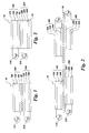
- Figure 1 shows schematically a light-emitting device 10.
- Light-emitting device 10 comprises organic EL elements 100 and 200 arranged in a stack and separated by an electrically insulating material 50, wherein at least a portion of organic EL element 100 overlaps at least a portion of organic EL element 200.
- Organic EL element 100 comprises a first organic EL material 130 disposed between first electrode 120 and second electrode 140.
- organic EL element 200 comprises a second organic EL material 230 disposed between first electrode 220 and second electrode 240.
- Insulating material 50 comprises a substantially transparent material, such as a glass or a substantially transparent plastic material.
- Organic EL elements 100 and 200 are provided with power supplies 110 and 210, respectively.
- voltages V 100 and V 200 supplied to organic EL elements 100 and 200 have different values, which are chosen to generate a desired brightness from the combined light-emitting device 10.
- each of voltages V 100 and V 200 can be chosen independently such that one organic EL material (130 or 230) is not exposed to a relatively higher voltage level that may be required by another EL material.
- power supplies 110 and 210 provide currents of different values to organic elements 100 and 200.
- Figure 1 shows two organic EL elements 100 and 200, it should be understood that more than two organic EL elements may be included in a light-emitting device 10 of the present invention.
- first electrodes 120 and 220 are anodes
- second electrodes 140 and 240 are cathodes.
- the order of the first and second electrodes in one organic EL element may be reversed.
- light-emitting device 10 is disposed on a substrate 70, as shown in Figure 3 .
- Substrate 70 may comprise glass or a substantially transparent plastic material.
- organic EL materials 130 and 230 comprise the same material.
- organic EL materials 130 and 230 comprise different materials.
- each EL material can emit in a different wavelength range.
- a light-emitting device comprising three organic EL elements arranged in a stack, emitting in the blue, green, and red wavelength ranges separately.
- each organic EL element can emit substantially in a wavelength range selected from the group consisting of 400-480 nm, 480-580 nm, and 580-700 nm.
- a light-emitting device can provide white light from the mixture of light from the individual EL elements.
- the brightness of an organic EL material typically increases monotonically with applied voltage within a reasonable voltage range, as shown in Figure 4 .
- a plurality of organic EL elements that are arranged in a stack and each activated at a low voltage can provide a total brightness that is substantially the same as that provided by a single organic EL element activated at a much higher voltage.
- Operating organic EL elements at a lower voltage (or current density) in the present invention results in a longer life of the EL elements, as is illustrated in Figure 5 for a blue light-emitting polymer.
- light-emitting device 10 comprising two substantially identical organic EL elements which are arranged in a stack and each of which is operated at bias voltage V 1 can provide the same total brightness of 2B as a single organic EL element that must be operated at bias voltage V 2 > V 1 (see Figure 4 ).
- the anode 120 (or 220) of organic EL element 100 (or 200) comprises a material having a high work function; e.g., greater than about 4.4 eV, for example from about 5 eV to about 7 eV.
- Indium tin oxide (“ITO") is typically used for this purpose.
- ITO is substantially transparent to light transmission and allows light emitted from organic EL layer 130 (or 230) easily to escape through the ITO anode layer without being seriously attenuated.
- substantially transparent means allowing at least 50 percent, preferably at least 80 percent, and more preferably at least 90 percent, of light in the visible wavelength range transmitted through a film having a thickness of about 0.5 micrometer, at an incident angle of less than or equal to 10 degrees.
- anode layer 120 Other materials suitable for use as the anode layer are tin oxide, indium oxide, zinc oxide, indium zinc oxide, zinc indium tin oxide, antimony oxide, and mixtures thereof. Still other usable materials for anode layer 120 are carbon nanotubes, or metals, such as silver or gold.
- Anode layer 120 may be deposited on the underlying element by physical vapor deposition, chemical vapor deposition, or sputtering.
- the thickness of an anode comprising such an electrically conducting oxide can be in the range from about 10 nm to about 500 nm, preferably from about 10 nm to about 200 nm, and more preferably from about 50 nm to about 200 nm.
- a thin, substantially transparent layer of a metal is also suitable; for example, a layer having a thickness less than about 50 nm, preferably less than about 20 nm.
- Suitable metals for anode 120 are those having high work function, such as greater than about 4.4 eV, for example, silver, copper, tungsten, nickel, cobalt, iron, selenium, germanium, gold, platinum, aluminum, or mixtures thereof or alloys thereof.
- Cathode 140 injecting negative charge carriers (electrons) into organic EL layer 130 (or 230) and is made of a material having a low work function; e.g., less than about 4 eV.
- Low-work function materials suitable for use as a cathode are K, Li, Na, Mg, Ca, Sr, Ba, Al, Ag, Au, In, Sn, Zn, Zr, Sc, Y, elements of the lanthanide series, alloys thereof, or mixtures thereof.
- Suitable alloy materials for the manufacture of cathode layer 140 are Ag-Mg, Al-Li, In-Mg, and Al-Ca alloys.
- Layered non-alloy structures are also possible, such as a thin layer of a metal such as Ca (thickness from about 1 to about 10 nm) or a non-metal such as LiF, KF, or NaF, covered by a thicker layer of some other metal, such as aluminum or silver.
- Cathode 140 may be deposited on the underlying element by physical vapor deposition, chemical vapor deposition, or sputtering.
- an electron-donating material chosen from among those disclosed above lowered the work function of cathode materials, thus reducing the barrier for electron injection and/or transport into organic EL material 130.
- cathode 140 (or 240) is substantially transparent.
- a substantially transparent cathode that is made of a material selected from the group consisting of ITO, tin oxide, indium oxide, zinc oxide, indium zinc oxide, zinc indium tin oxide, antimony oxide, and mixtures thereof. Materials such as carbon nanotubes may also be used as cathode material.
- Organic EL layer 130 (or 230) serves as the transport medium for both holes and electrons. In this layer these excited species combine and drop to a lower energy level, concurrently emitting EM radiation in the visible range.
- Organic EL materials are chosen to electroluminesce in the desired wavelength range. The thickness of the organic EL layer 130 is preferably kept in the range of about 100 to about 300 nm.
- the organic EL material may be a polymer, a copolymer, a mixture of polymers, or lower molecular-weight organic molecules having unsaturated bonds. Such materials possess a delocalized ⁇ -electron system, which gives the polymer chains or organic molecules the ability to support positive and negative charge carriers with high mobility.
- Suitable EL polymers are poly(N-vinylcarbazole) ("PVK", emitting violet-to-blue light in the wavelengths of about 380-500 nm) and its derivatives; polyfluorene and its derivatives such as poly(alkylfluorene), for example poly(9,9-dihexylfluorene) (410-550 nm), poly(dioctylfluorene) (wavelength at peak EL emission of 436 nm) or poly ⁇ 9,9-bis(3,6-dioxaheptyl)-fluorene-2,7-diyl ⁇ (400-550 nm); poly(praraphenylene) (“PPP”) and its derivatives such as poly(2-decyloxy-1,4-phenylene) (400-550 nm) or poly(2,5-diheptyl-1,4-phenylene); poly(p-phenylene vinylene) (“PPV”) and its derivatives
- polysilanes are linear silicon-backbone polymers substituted with a variety of alkyl and/or aryl side groups. They are quasi one-dimensional materials with delocalized ⁇ -conjugated electrons along polymer backbone chains. Examples of polysilanes are poly(di-n-butylsilane), poly(di-n-pentylsilane), poly(di-n-hexylsilane), poly(methylphenylsilane), and poly ⁇ bis(p-butylphenyl)silane ⁇ which are disclosed in H.
- Organic materials having molecular weight less than, for example, about 5000 that are made of a large number of aromatic units are also applicable.
- An example of such materials is 1,3,5-tris ⁇ n-(4-diphenylaminophenyl) phenylamino ⁇ benzene, which emits light in the wavelength range of 380-500 nm.
- the organic EL layer also may be prepared from lower molecular weight organic molecules, such as phenylanthracene, tetraarylethene, coumarin, rubrene, tetraphenylbutadiene, anthracene, perylene, coronene, or their derivatives. These materials generally emit light having maximum wavelength of about 520 nm.
- Still other suitable materials are the low molecular-weight metal organic complexes such as aluminum-, gallium-, and indium-acetylacetonate, which emit light in the wavelength range of 415-457 nm, aluminum-(picolymethylketone)-bis ⁇ 2,6-di(t-butyl)phenoxide ⁇ or scandium-(4-methoxy-picolylmethylketone)-bis(acetylacetonate), which emits in the range of 420-433 nm.
- the preferred organic EL materials are those emit light in the blue-green wavelengths.
- organo-metallic complexes of 8-hydroxyquinoline such as tris(8-quinolinolato)aluminum and its derivatives.
- organic EL materials are disclosed in U. Mitschke and P. Bauerle, "The Electroluminescence of Organic Materials," J. Mater. Chem., Vol. 10, pp. 1471-1507 (2000 ).
- An organic EL material is deposited on the underlying layer (e.g., an electrode layer) by physical or chemical vapor deposition, spin coating, dip coating, spraying, ink-jet printing, gravure coating, flexo-coating, screen printing, or casting, followed by polymerization, if necessary, or curing of the material.
- the organic EL material may be diluted in a solvent to adjust its viscosity or mixed with another polymeric material that serves as a film-forming vehicle.
- one or more additional layers may be included in light-emitting element 100 further to increase the efficiency thereof.
- an additional layer can serve to improve the injection and/or transport of positive charges (holes) into the organic EL layer 130.
- the thickness of each of these layers is kept to below 500 nm, preferably below 100 nm.
- Suitable materials for these additional layers are low-to-intermediate molecular weight (for example, less than about 2000) organic molecules, poly(3,4-ethylenedioxythipohene) (“PEDOT”), and polyaniline. They may be applied during the manufacture of the element 100 by conventional methods such as spray coating, dip coating, gravure coating, flexo-coating, screen printing, or physical or chemical vapor deposition.
- a hole injection enhancement layer 122 is formed between the anode layer 120 and the organic EL layer 130 to provide a higher injected current at a given forward bias and/or a higher maximum current before the failure of the device.
- the hole injection enhancement layer facilitates the injection of holes from the anode.
- Suitable materials for the hole injection enhancement layer are arylene-based compounds disclosed in US Patent 5,998,803 ; such as 3,4,9,10-perylenetetra-carboxylic dianhydride or bis(1,2,5-thiadiazolo)-p-quinobis(1,3-dithiole).
- light-emitting device 10 further includes a hole transport layer 124 which is disposed between the hole injection enhancement layer 122 and the organic EL layer 130.
- the hole transport layer 124 has the functions of transporting holes and blocking the transportation of electrons so that holes and electrons are optimally combined in the organic EL layer 130.
- Materials suitable for the hole transport layer are triaryldiamine, tetraphenyldiamine, aromatic tertiary amines, hydrazone derivatives, carbazole derivatives, triazole derivatives, imidazole derivatives, oxadiazole derivatives having an amino group, and polythiophenes as disclosed in US Patent 6,023,371 .
- light-emitting element 100 includes an additional layer 154 which can be disposed between cathode 140 and organic EL layer 130.
- Layer 154 can further enhance the injection and transport of electrons (hereinafter called “electron injecting and transporting enhancement layer”) to organic EL layer 130.
- Materials suitable for the electron injecting and transporting enhancement layer are metal organic complexes such as tris(8-quinolinolato)aluminum, oxadiazole derivatives, perylene derivatives, pyridine derivatives, pyrimidine derivatives, quinoline derivatives, quinoxaline derivatives, diphenylquinone derivatives, and nitro-substituted fluorene derivatives, as disclosed in US Patent 6,023,371 .
- metal organic complexes such as tris(8-quinolinolato)aluminum, oxadiazole derivatives, perylene derivatives, pyridine derivatives, pyrimidine derivatives, quinoline derivatives, quinoxaline derivatives, diphenylquinone derivatives, and nitro-substituted fluorene derivatives, as disclosed in US Patent 6,023,371 .
- Organic EL elements were fabricated. Each includes an organic EL polymer emitting blue, green, or red light.
- the organic EL polymers were purchased from American Dye Source, Inc. (Baie d'Urfe, Quebec, Canada), having catalog numbers ADS329BE (blue light-emitting), ADS132GE (green light-emitting), and ADS200RE (red light-emitting).
- ADS329BE is poly(9,9-dioctylfluorenyl-2,7-diyl) end capped with N,N'-bis(4-methylphenyl-4-aniline).
- ADS132GE is poly(9,9-dioctylfluorenyl-2,7-diyl)-alt-co-(N,N'-diphenyl)-N,N'-di(p-butyl-oxyphenyl)-1,4-diaminobenzene.
- ADS200RE is poly ⁇ 2-methoxy-5-(2-ethylhexyloxy)-1,4-phenylenevinylene ⁇ end capped with polyhedral oligomeric silsesquioxanes.
- Stacking a plurality of organic EL elements also provides a benefit of producing a more uniform brightness because the brightness nonuniformity of one organic EL element can be mitigated by another organic EL element in the stack.
- This situation occurs, for example, when a pair of electrodes is disposed in contact with the two opposite edges of a sheet of an organic EL material. Since the sheet of most transparent conductors/electrodes has a finite resistance, the brightness of the EL element decreases continuously from anode to cathode.
- a second organic EL element of the same construction is disposed on the first organic EL element such that the direction of current flow in the second element is opposite to that in the first element. This arrangement produces a more uniform brightness from the total device.
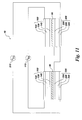
- At least two stacks of organic EL elements are disposed adjacent to one another.
- the organic EL elements in a single stack are electrically separate, but organic EL elements of adjacent stacks, one from each stack, are electrically connected in series, as shown in Figure 11 .
- Each of such series is independently controlled such that only a voltage desired for such series is imposed thereon.
- Figure 11 shows two stacks of organic EL elements, each having two elements, the present invention is equally applicable to any number of stacks, each having any number of elements greater than at least two.
- the organic EL materials of the organic EL elements of a single stack comprise different materials. Furthermore, they can emit different light colors. In another embodiment, the organic EL materials of organic EL elements that are connected electrically in-series comprise the same material, while the organic EL materials of the organic EL elements of a single stack comprise different materials.
- a method of making a light-emitting device is provided according to claim 6.
- a method of making a light-emitting device comprises: (a) providing a substrate; (b) disposing a first organic EL element on the substrate; (c) disposing an electrically non-conducting material on the first organic EL element; (d) disposing a second organic EL element on the electrically non-conducting material; wherein each organic EL element comprises an organic EL material sandwiched between a first electrode and a second electrode, and the electrically non-conducting material electrically separates the first and second organic EL elements.
- the step of disposing an organic EL element comprises: (1) disposing a first electrically conducting material on an underlying layer; (2) disposing an organic EL material on the first electrically conducting material; and (3) disposing a second electrically conducting material on the organic EL material.
- the step of disposing an electrically conducting material is effected by a method selected from the group consisting of physical vapor deposition, chemical vapor deposition, and sputtering.
- the step of disposing an organic EL material is effected by a method selected from the group consisting of physical vapor deposition, chemical vapor deposition, spin coating, dip coating, spraying, ink-jet printing, and casting.
- the step of disposing is followed by polymerization, if necessary, or curing of the organic EL material.
- a method of generating light comprises providing an independent voltage to each organic EL element of a stack of organic EL elements, according to claim 7.
- the voltage applied to an organic EL element is different from that applied to another organic EL element.
Landscapes
- Physics & Mathematics (AREA)
- Optics & Photonics (AREA)
- Electroluminescent Light Sources (AREA)
Applications Claiming Priority (2)
| Application Number | Priority Date | Filing Date | Title |
|---|---|---|---|
| US10/870,865 US7227305B2 (en) | 2004-06-18 | 2004-06-18 | Stacked organic electroluminescent devices |
| PCT/US2005/011755 WO2006006975A1 (en) | 2004-06-18 | 2005-04-07 | Stacked organic electroluminescent devices |
Publications (2)
| Publication Number | Publication Date |
|---|---|
| EP1766684A1 EP1766684A1 (en) | 2007-03-28 |
| EP1766684B1 true EP1766684B1 (en) | 2015-09-30 |
Family
ID=35159822
Family Applications (1)
| Application Number | Title | Priority Date | Filing Date |
|---|---|---|---|
| EP05735229.6A Expired - Lifetime EP1766684B1 (en) | 2004-06-18 | 2005-04-07 | Stacked organic electroluminescent devices |
Country Status (7)
| Country | Link |
|---|---|
| US (1) | US7227305B2 (enExample) |
| EP (1) | EP1766684B1 (enExample) |
| JP (1) | JP2008503055A (enExample) |
| KR (2) | KR101295988B1 (enExample) |
| CN (1) | CN100543987C (enExample) |
| TW (1) | TWI389594B (enExample) |
| WO (1) | WO2006006975A1 (enExample) |
Families Citing this family (35)
| Publication number | Priority date | Publication date | Assignee | Title |
|---|---|---|---|---|
| US20080075872A1 (en) * | 1999-08-04 | 2008-03-27 | Lichtenhan Joseph D | Nanoscopic Assurance Coating for Lead-Free Solders |
| GB2410600A (en) * | 2004-01-30 | 2005-08-03 | Cambridge Display Tech Ltd | Organic light emitting diode display device |
| JP2006010986A (ja) * | 2004-06-24 | 2006-01-12 | Kyocera Corp | 画像表示装置 |
| US20060006792A1 (en) * | 2004-07-09 | 2006-01-12 | Eastman Kodak Company | Flat panel light emitting devices with two sided |
| US20070194308A1 (en) * | 2005-06-27 | 2007-08-23 | Wintek Corporation | Organic light emitting display capable of showing images on double sides thereof |
| US7531959B2 (en) * | 2005-06-29 | 2009-05-12 | Eastman Kodak Company | White light tandem OLED display with filters |
| EP1784055A3 (en) * | 2005-10-17 | 2009-08-05 | Semiconductor Energy Laboratory Co., Ltd. | Lighting system |
| US7843134B2 (en) * | 2005-10-31 | 2010-11-30 | Idemitsu Kosan Co., Ltd. | Organic EL emission devices connected in series |
| US8138075B1 (en) | 2006-02-06 | 2012-03-20 | Eberlein Dietmar C | Systems and methods for the manufacture of flat panel devices |
| US7667383B2 (en) * | 2006-02-15 | 2010-02-23 | Osram Opto Semiconductors Gmbh | Light source comprising a common substrate, a first led device and a second led device |
| US20080007936A1 (en) * | 2006-07-05 | 2008-01-10 | Jie Liu | Organic illumination source and method for controlled illumination |
| US9226363B2 (en) * | 2006-11-22 | 2015-12-29 | Samsung Electronics Co., Ltd. | Electroluminescent devices having nanostructure-film electrode(s) |
| US7498603B2 (en) * | 2006-12-06 | 2009-03-03 | General Electric Company | Color tunable illumination source and method for controlled illumination |
| US20080137008A1 (en) * | 2006-12-06 | 2008-06-12 | General Electric Company | Color tunable oled illumination display and method for controlled display illumination |
| US7804245B2 (en) * | 2008-01-24 | 2010-09-28 | Global Oled Technology Llc | Electroluminescent device having improved brightness uniformity |
| US8115399B2 (en) * | 2008-02-19 | 2012-02-14 | General Electric Company | OLED light source |
| US20090284158A1 (en) * | 2008-05-16 | 2009-11-19 | General Electric Company | Organic light emitting device based lighting for low cost, flexible large area signage |
| JP5217844B2 (ja) * | 2008-09-26 | 2013-06-19 | コニカミノルタホールディングス株式会社 | 照明用面発光パネル |
| WO2011117814A1 (en) * | 2010-03-25 | 2011-09-29 | Koninklijke Philips Electronics N.V. | A light emitting device, a color tunable light, an animation presentation device and a luminaire |
| KR20110112641A (ko) * | 2010-04-07 | 2011-10-13 | 한국과학기술연구원 | 광활성 그룹을 측쇄로 가지는 사다리 구조의 폴리실세스퀴옥산 및 이의 제조방법 |
| TW201304225A (zh) * | 2011-07-13 | 2013-01-16 | Au Optronics Corp | 有機電激發光光源 |
| CN102891262A (zh) * | 2011-07-22 | 2013-01-23 | 海洋王照明科技股份有限公司 | 叠层有机电致发光器件及其制备方法 |
| US20180019433A1 (en) * | 2011-10-26 | 2018-01-18 | Koninklijke Philips N.V. | Masking for light emitting device patterns |
| US10032834B2 (en) * | 2012-08-09 | 2018-07-24 | Sony Corporation | Light receiving/emitting element and light receiving/emitting apparatus |
| US9706620B2 (en) * | 2013-03-28 | 2017-07-11 | Empire Technology Development Llc | Methods and compositions for producing polarized light |
| CN104124392A (zh) * | 2013-04-24 | 2014-10-29 | 海洋王照明科技股份有限公司 | 一种有机电致发光器件及其制备方法 |
| KR101877195B1 (ko) | 2013-06-13 | 2018-07-10 | 코니카 미놀타 가부시키가이샤 | 유기 일렉트로루미네센스 소자의 구동 방법 |
| JP5857006B2 (ja) * | 2013-07-31 | 2016-02-10 | Lumiotec株式会社 | 有機エレクトロルミネッセント素子及び照明装置 |
| US10141378B2 (en) | 2013-10-30 | 2018-11-27 | Industrial Technology Research Institute | Light emitting device free of TFT and chiplet |
| TWI586012B (zh) * | 2014-01-02 | 2017-06-01 | 財團法人工業技術研究院 | 發光元件 |
| CN103956434A (zh) * | 2014-04-14 | 2014-07-30 | 上海大学 | 基于oled调制的双面有机电致发光器件及其制备方法 |
| RU2631015C1 (ru) * | 2016-04-29 | 2017-09-15 | Федеральное государственное бюджетное образовательное учреждение высшего профессионального образования "Томский государственный университет систем управления и радиоэлектроники" | Высоковольтное органическое люминесцентное устройство |
| CN107946343A (zh) * | 2017-11-15 | 2018-04-20 | 江苏集萃有机光电技术研究所有限公司 | 像素结构及oled面板 |
| CN110957347A (zh) * | 2019-12-13 | 2020-04-03 | 苏州星烁纳米科技有限公司 | 一种发光结构、显示装置及照明装置 |
| CN115697813A (zh) * | 2020-06-12 | 2023-02-03 | 株式会社半导体能源研究所 | 车辆控制装置 |
Family Cites Families (14)
| Publication number | Priority date | Publication date | Assignee | Title |
|---|---|---|---|---|
| JP4477150B2 (ja) | 1996-01-17 | 2010-06-09 | 三星モバイルディスプレイ株式會社 | 有機薄膜el素子 |
| US5677572A (en) | 1996-07-29 | 1997-10-14 | Eastman Kodak Company | Bilayer electrode on a n-type semiconductor |
| US5998803A (en) | 1997-05-29 | 1999-12-07 | The Trustees Of Princeton University | Organic light emitting device containing a hole injection enhancement layer |
| US5917280A (en) | 1997-02-03 | 1999-06-29 | The Trustees Of Princeton University | Stacked organic light emitting devices |
| JPH10338872A (ja) | 1997-06-09 | 1998-12-22 | Tdk Corp | 色変換材料およびこれを用いた有機elカラーディスプレイ |
| US5965907A (en) * | 1997-09-29 | 1999-10-12 | Motorola, Inc. | Full color organic light emitting backlight device for liquid crystal display applications |
| JP3884564B2 (ja) | 1998-05-20 | 2007-02-21 | 出光興産株式会社 | 有機el発光素子およびそれを用いた発光装置 |
| JP4264994B2 (ja) | 1998-07-10 | 2009-05-20 | 凸版印刷株式会社 | 有機エレクトロルミネッセンス表示素子の製造方法 |
| JP2001135479A (ja) | 1999-11-08 | 2001-05-18 | Canon Inc | 発光素子、並びにそれを用いた画像読取装置、情報処理装置及びディスプレイ装置 |
| JP2004031214A (ja) * | 2002-06-27 | 2004-01-29 | Matsushita Electric Ind Co Ltd | 有機電界発光素子 |
| US7034470B2 (en) * | 2002-08-07 | 2006-04-25 | Eastman Kodak Company | Serially connecting OLED devices for area illumination |
| US6693296B1 (en) | 2002-08-07 | 2004-02-17 | Eastman Kodak Company | OLED apparatus including a series of OLED devices |
| US7012364B2 (en) * | 2002-10-01 | 2006-03-14 | Dai Nippon Printing Co., Ltd. | Organic electroluminescent display |
| JP2005005223A (ja) * | 2003-06-13 | 2005-01-06 | Matsushita Electric Ind Co Ltd | 発光素子および表示デバイス |
-
2004
- 2004-06-18 US US10/870,865 patent/US7227305B2/en not_active Expired - Lifetime
-
2005
- 2005-04-07 KR KR1020067026552A patent/KR101295988B1/ko not_active Expired - Lifetime
- 2005-04-07 WO PCT/US2005/011755 patent/WO2006006975A1/en not_active Ceased
- 2005-04-07 KR KR1020137008579A patent/KR20130052637A/ko not_active Ceased
- 2005-04-07 JP JP2007516466A patent/JP2008503055A/ja active Pending
- 2005-04-07 EP EP05735229.6A patent/EP1766684B1/en not_active Expired - Lifetime
- 2005-04-07 CN CNB2005800200007A patent/CN100543987C/zh not_active Expired - Lifetime
- 2005-06-06 TW TW094118612A patent/TWI389594B/zh not_active IP Right Cessation
Also Published As
| Publication number | Publication date |
|---|---|
| KR101295988B1 (ko) | 2013-08-13 |
| CN100543987C (zh) | 2009-09-23 |
| US7227305B2 (en) | 2007-06-05 |
| KR20130052637A (ko) | 2013-05-22 |
| EP1766684A1 (en) | 2007-03-28 |
| TWI389594B (zh) | 2013-03-11 |
| KR20070027589A (ko) | 2007-03-09 |
| WO2006006975A1 (en) | 2006-01-19 |
| TW200610436A (en) | 2006-03-16 |
| US20050280359A1 (en) | 2005-12-22 |
| JP2008503055A (ja) | 2008-01-31 |
| CN1969385A (zh) | 2007-05-23 |
Similar Documents
| Publication | Publication Date | Title |
|---|---|---|
| EP1766684B1 (en) | Stacked organic electroluminescent devices | |
| US7368659B2 (en) | Electrodes mitigating effects of defects in organic electronic devices | |
| EP2245683B1 (en) | Organic light emitting device and method for manufacturing the same | |
| US7768210B2 (en) | Hybrid electroluminescent devices | |
| US20020020924A1 (en) | Novel organic opto-electronic devices and method for making the same | |
| US7411223B2 (en) | Compound electrodes for electronic devices | |
| US7242141B2 (en) | Integrated fuses for OLED lighting device | |
| EP1610397B1 (en) | Metal compound-metal multilayer electrodes for organic electronic devices | |
| US8525163B2 (en) | Organic EL device, method for fabricating organic EL device, and organic EL illumination system | |
| JP2009520321A (ja) | 電気活性デバイス用積層電極及びその製造方法 | |
| US20060012289A1 (en) | Hybrid electroluminescent devices | |
| CN102845131A (zh) | 发光装置 | |
| Shiang et al. | Hybrid electroluminescent devices |
Legal Events
| Date | Code | Title | Description |
|---|---|---|---|
| PUAI | Public reference made under article 153(3) epc to a published international application that has entered the european phase |
Free format text: ORIGINAL CODE: 0009012 |
|
| 17P | Request for examination filed |
Effective date: 20070118 |
|
| AK | Designated contracting states |
Kind code of ref document: A1 Designated state(s): AT BE BG CH CY CZ DE DK EE ES FI FR GB GR HU IE IS IT LI LT LU MC NL PL PT RO SE SI SK TR |
|
| RAP1 | Party data changed (applicant data changed or rights of an application transferred) |
Owner name: GENERAL ELECTRIC COMPANY |
|
| DAX | Request for extension of the european patent (deleted) | ||
| 17Q | First examination report despatched |
Effective date: 20071128 |
|
| REG | Reference to a national code |
Ref country code: DE Ref legal event code: R079 Ref document number: 602005047602 Country of ref document: DE Free format text: PREVIOUS MAIN CLASS: H01L0027000000 Ipc: H01L0027320000 |
|
| GRAP | Despatch of communication of intention to grant a patent |
Free format text: ORIGINAL CODE: EPIDOSNIGR1 |
|
| RIC1 | Information provided on ipc code assigned before grant |
Ipc: H01L 27/32 20060101AFI20150410BHEP |
|
| INTG | Intention to grant announced |
Effective date: 20150518 |
|
| GRAS | Grant fee paid |
Free format text: ORIGINAL CODE: EPIDOSNIGR3 |
|
| GRAA | (expected) grant |
Free format text: ORIGINAL CODE: 0009210 |
|
| AK | Designated contracting states |
Kind code of ref document: B1 Designated state(s): AT BE BG CH CY CZ DE DK EE ES FI FR GB GR HU IE IS IT LI LT LU MC NL PL PT RO SE SI SK TR |
|
| REG | Reference to a national code |
Ref country code: CH Ref legal event code: EP Ref country code: GB Ref legal event code: FG4D |
|
| REG | Reference to a national code |
Ref country code: DE Ref legal event code: R081 Ref document number: 602005047602 Country of ref document: DE Owner name: BOE TECHNOLOGY GROUP CO., LTD., CN Free format text: FORMER OWNER: GENERAL ELECTRIC CO., SCHENECTADY, N.Y., US |
|
| REG | Reference to a national code |
Ref country code: AT Ref legal event code: REF Ref document number: 752877 Country of ref document: AT Kind code of ref document: T Effective date: 20151015 |
|
| REG | Reference to a national code |
Ref country code: IE Ref legal event code: FG4D |
|
| REG | Reference to a national code |
Ref country code: DE Ref legal event code: R096 Ref document number: 602005047602 Country of ref document: DE |
|
| PG25 | Lapsed in a contracting state [announced via postgrant information from national office to epo] |
Ref country code: GR Free format text: LAPSE BECAUSE OF FAILURE TO SUBMIT A TRANSLATION OF THE DESCRIPTION OR TO PAY THE FEE WITHIN THE PRESCRIBED TIME-LIMIT Effective date: 20151231 Ref country code: LT Free format text: LAPSE BECAUSE OF FAILURE TO SUBMIT A TRANSLATION OF THE DESCRIPTION OR TO PAY THE FEE WITHIN THE PRESCRIBED TIME-LIMIT Effective date: 20150930 Ref country code: FI Free format text: LAPSE BECAUSE OF FAILURE TO SUBMIT A TRANSLATION OF THE DESCRIPTION OR TO PAY THE FEE WITHIN THE PRESCRIBED TIME-LIMIT Effective date: 20150930 |
|
| REG | Reference to a national code |
Ref country code: LT Ref legal event code: MG4D Ref country code: NL Ref legal event code: FP |
|
| REG | Reference to a national code |
Ref country code: AT Ref legal event code: MK05 Ref document number: 752877 Country of ref document: AT Kind code of ref document: T Effective date: 20150930 |
|
| PG25 | Lapsed in a contracting state [announced via postgrant information from national office to epo] |
Ref country code: SE Free format text: LAPSE BECAUSE OF FAILURE TO SUBMIT A TRANSLATION OF THE DESCRIPTION OR TO PAY THE FEE WITHIN THE PRESCRIBED TIME-LIMIT Effective date: 20150930 |
|
| PG25 | Lapsed in a contracting state [announced via postgrant information from national office to epo] |
Ref country code: ES Free format text: LAPSE BECAUSE OF FAILURE TO SUBMIT A TRANSLATION OF THE DESCRIPTION OR TO PAY THE FEE WITHIN THE PRESCRIBED TIME-LIMIT Effective date: 20150930 Ref country code: IS Free format text: LAPSE BECAUSE OF FAILURE TO SUBMIT A TRANSLATION OF THE DESCRIPTION OR TO PAY THE FEE WITHIN THE PRESCRIBED TIME-LIMIT Effective date: 20160130 Ref country code: SK Free format text: LAPSE BECAUSE OF FAILURE TO SUBMIT A TRANSLATION OF THE DESCRIPTION OR TO PAY THE FEE WITHIN THE PRESCRIBED TIME-LIMIT Effective date: 20150930 Ref country code: EE Free format text: LAPSE BECAUSE OF FAILURE TO SUBMIT A TRANSLATION OF THE DESCRIPTION OR TO PAY THE FEE WITHIN THE PRESCRIBED TIME-LIMIT Effective date: 20150930 Ref country code: CZ Free format text: LAPSE BECAUSE OF FAILURE TO SUBMIT A TRANSLATION OF THE DESCRIPTION OR TO PAY THE FEE WITHIN THE PRESCRIBED TIME-LIMIT Effective date: 20150930 Ref country code: IT Free format text: LAPSE BECAUSE OF FAILURE TO SUBMIT A TRANSLATION OF THE DESCRIPTION OR TO PAY THE FEE WITHIN THE PRESCRIBED TIME-LIMIT Effective date: 20150930 |
|
| REG | Reference to a national code |
Ref country code: NL Ref legal event code: PD Owner name: BOE TECHNOLOGY GROUP CO., LTD.; CN Free format text: DETAILS ASSIGNMENT: VERANDERING VAN EIGENAAR(S), OVERDRACHT; FORMER OWNER NAME: GENERAL ELECTRIC COMPANY Effective date: 20160520 |
|
| REG | Reference to a national code |
Ref country code: DE Ref legal event code: R081 Ref document number: 602005047602 Country of ref document: DE Owner name: BOE TECHNOLOGY GROUP CO., LTD., CN Free format text: FORMER OWNER: GENERAL ELECTRIC COMPANY, SCHENECTADY, NY, US Ref country code: DE Ref legal event code: R081 Ref document number: 602005047602 Country of ref document: DE Owner name: BOE TECHNOLOGY GROUP CO., LTD., CN Free format text: FORMER OWNER: GENERAL ELECTRIC COMPANY, SCHENECTADY, N.Y., US |
|
| PG25 | Lapsed in a contracting state [announced via postgrant information from national office to epo] |
Ref country code: PT Free format text: LAPSE BECAUSE OF FAILURE TO SUBMIT A TRANSLATION OF THE DESCRIPTION OR TO PAY THE FEE WITHIN THE PRESCRIBED TIME-LIMIT Effective date: 20160201 Ref country code: AT Free format text: LAPSE BECAUSE OF FAILURE TO SUBMIT A TRANSLATION OF THE DESCRIPTION OR TO PAY THE FEE WITHIN THE PRESCRIBED TIME-LIMIT Effective date: 20150930 Ref country code: RO Free format text: LAPSE BECAUSE OF FAILURE TO SUBMIT A TRANSLATION OF THE DESCRIPTION OR TO PAY THE FEE WITHIN THE PRESCRIBED TIME-LIMIT Effective date: 20150930 Ref country code: PL Free format text: LAPSE BECAUSE OF FAILURE TO SUBMIT A TRANSLATION OF THE DESCRIPTION OR TO PAY THE FEE WITHIN THE PRESCRIBED TIME-LIMIT Effective date: 20150930 |
|
| REG | Reference to a national code |
Ref country code: DE Ref legal event code: R097 Ref document number: 602005047602 Country of ref document: DE |
|
| REG | Reference to a national code |
Ref country code: GB Ref legal event code: 732E Free format text: REGISTERED BETWEEN 20160616 AND 20160622 |
|
| PLBE | No opposition filed within time limit |
Free format text: ORIGINAL CODE: 0009261 |
|
| STAA | Information on the status of an ep patent application or granted ep patent |
Free format text: STATUS: NO OPPOSITION FILED WITHIN TIME LIMIT |
|
| PG25 | Lapsed in a contracting state [announced via postgrant information from national office to epo] |
Ref country code: DK Free format text: LAPSE BECAUSE OF FAILURE TO SUBMIT A TRANSLATION OF THE DESCRIPTION OR TO PAY THE FEE WITHIN THE PRESCRIBED TIME-LIMIT Effective date: 20150930 Ref country code: BE Free format text: LAPSE BECAUSE OF NON-PAYMENT OF DUE FEES Effective date: 20160430 |
|
| 26N | No opposition filed |
Effective date: 20160701 |
|
| PG25 | Lapsed in a contracting state [announced via postgrant information from national office to epo] |
Ref country code: SI Free format text: LAPSE BECAUSE OF FAILURE TO SUBMIT A TRANSLATION OF THE DESCRIPTION OR TO PAY THE FEE WITHIN THE PRESCRIBED TIME-LIMIT Effective date: 20150930 |
|
| REG | Reference to a national code |
Ref country code: CH Ref legal event code: PL |
|
| PG25 | Lapsed in a contracting state [announced via postgrant information from national office to epo] |
Ref country code: LU Free format text: LAPSE BECAUSE OF FAILURE TO SUBMIT A TRANSLATION OF THE DESCRIPTION OR TO PAY THE FEE WITHIN THE PRESCRIBED TIME-LIMIT Effective date: 20160407 Ref country code: BE Free format text: LAPSE BECAUSE OF FAILURE TO SUBMIT A TRANSLATION OF THE DESCRIPTION OR TO PAY THE FEE WITHIN THE PRESCRIBED TIME-LIMIT Effective date: 20150930 |
|
| REG | Reference to a national code |
Ref country code: IE Ref legal event code: MM4A |
|
| REG | Reference to a national code |
Ref country code: FR Ref legal event code: ST Effective date: 20161230 |
|
| PG25 | Lapsed in a contracting state [announced via postgrant information from national office to epo] |
Ref country code: FR Free format text: LAPSE BECAUSE OF NON-PAYMENT OF DUE FEES Effective date: 20160502 Ref country code: LI Free format text: LAPSE BECAUSE OF NON-PAYMENT OF DUE FEES Effective date: 20160430 Ref country code: CH Free format text: LAPSE BECAUSE OF NON-PAYMENT OF DUE FEES Effective date: 20160430 |
|
| PG25 | Lapsed in a contracting state [announced via postgrant information from national office to epo] |
Ref country code: IE Free format text: LAPSE BECAUSE OF NON-PAYMENT OF DUE FEES Effective date: 20160407 |
|
| REG | Reference to a national code |
Ref country code: DE Ref legal event code: R082 Ref document number: 602005047602 Country of ref document: DE Representative=s name: KLUNKER IP PATENTANWAELTE PARTG MBB, DE |
|
| PG25 | Lapsed in a contracting state [announced via postgrant information from national office to epo] |
Ref country code: CY Free format text: LAPSE BECAUSE OF FAILURE TO SUBMIT A TRANSLATION OF THE DESCRIPTION OR TO PAY THE FEE WITHIN THE PRESCRIBED TIME-LIMIT Effective date: 20150930 Ref country code: HU Free format text: LAPSE BECAUSE OF FAILURE TO SUBMIT A TRANSLATION OF THE DESCRIPTION OR TO PAY THE FEE WITHIN THE PRESCRIBED TIME-LIMIT; INVALID AB INITIO Effective date: 20050407 |
|
| PG25 | Lapsed in a contracting state [announced via postgrant information from national office to epo] |
Ref country code: TR Free format text: LAPSE BECAUSE OF FAILURE TO SUBMIT A TRANSLATION OF THE DESCRIPTION OR TO PAY THE FEE WITHIN THE PRESCRIBED TIME-LIMIT Effective date: 20150930 Ref country code: MC Free format text: LAPSE BECAUSE OF FAILURE TO SUBMIT A TRANSLATION OF THE DESCRIPTION OR TO PAY THE FEE WITHIN THE PRESCRIBED TIME-LIMIT Effective date: 20150930 |
|
| PG25 | Lapsed in a contracting state [announced via postgrant information from national office to epo] |
Ref country code: BG Free format text: LAPSE BECAUSE OF FAILURE TO SUBMIT A TRANSLATION OF THE DESCRIPTION OR TO PAY THE FEE WITHIN THE PRESCRIBED TIME-LIMIT Effective date: 20150930 |
|
| REG | Reference to a national code |
Ref country code: DE Ref legal event code: R079 Ref document number: 602005047602 Country of ref document: DE Free format text: PREVIOUS MAIN CLASS: H01L0027320000 Ipc: H10K0059000000 |
|
| PGFP | Annual fee paid to national office [announced via postgrant information from national office to epo] |
Ref country code: GB Payment date: 20240312 Year of fee payment: 20 |
|
| PGFP | Annual fee paid to national office [announced via postgrant information from national office to epo] |
Ref country code: NL Payment date: 20240422 Year of fee payment: 20 |
|
| PGFP | Annual fee paid to national office [announced via postgrant information from national office to epo] |
Ref country code: DE Payment date: 20240418 Year of fee payment: 20 |
|
| REG | Reference to a national code |
Ref country code: DE Ref legal event code: R071 Ref document number: 602005047602 Country of ref document: DE |
|
| REG | Reference to a national code |
Ref country code: NL Ref legal event code: MK Effective date: 20250406 |
|
| REG | Reference to a national code |
Ref country code: GB Ref legal event code: PE20 Expiry date: 20250406 |
|
| PG25 | Lapsed in a contracting state [announced via postgrant information from national office to epo] |
Ref country code: GB Free format text: LAPSE BECAUSE OF EXPIRATION OF PROTECTION Effective date: 20250406 |