EP1764771A2 - Organic electroluminescent display device - Google Patents
Organic electroluminescent display device Download PDFInfo
- Publication number
- EP1764771A2 EP1764771A2 EP06120752A EP06120752A EP1764771A2 EP 1764771 A2 EP1764771 A2 EP 1764771A2 EP 06120752 A EP06120752 A EP 06120752A EP 06120752 A EP06120752 A EP 06120752A EP 1764771 A2 EP1764771 A2 EP 1764771A2
- Authority
- EP
- European Patent Office
- Prior art keywords
- transistor
- scan
- data
- voltage
- display device
- Prior art date
- Legal status (The legal status is an assumption and is not a legal conclusion. Google has not performed a legal analysis and makes no representation as to the accuracy of the status listed.)
- Withdrawn
Links
Images


Classifications
-
- G—PHYSICS
- G09—EDUCATION; CRYPTOGRAPHY; DISPLAY; ADVERTISING; SEALS
- G09G—ARRANGEMENTS OR CIRCUITS FOR CONTROL OF INDICATING DEVICES USING STATIC MEANS TO PRESENT VARIABLE INFORMATION
- G09G3/00—Control arrangements or circuits, of interest only in connection with visual indicators other than cathode-ray tubes
- G09G3/20—Control arrangements or circuits, of interest only in connection with visual indicators other than cathode-ray tubes for presentation of an assembly of a number of characters, e.g. a page, by composing the assembly by combination of individual elements arranged in a matrix no fixed position being assigned to or needed to be assigned to the individual characters or partial characters
- G09G3/22—Control arrangements or circuits, of interest only in connection with visual indicators other than cathode-ray tubes for presentation of an assembly of a number of characters, e.g. a page, by composing the assembly by combination of individual elements arranged in a matrix no fixed position being assigned to or needed to be assigned to the individual characters or partial characters using controlled light sources
- G09G3/30—Control arrangements or circuits, of interest only in connection with visual indicators other than cathode-ray tubes for presentation of an assembly of a number of characters, e.g. a page, by composing the assembly by combination of individual elements arranged in a matrix no fixed position being assigned to or needed to be assigned to the individual characters or partial characters using controlled light sources using electroluminescent panels
- G09G3/32—Control arrangements or circuits, of interest only in connection with visual indicators other than cathode-ray tubes for presentation of an assembly of a number of characters, e.g. a page, by composing the assembly by combination of individual elements arranged in a matrix no fixed position being assigned to or needed to be assigned to the individual characters or partial characters using controlled light sources using electroluminescent panels semiconductive, e.g. using light-emitting diodes [LED]
- G09G3/3208—Control arrangements or circuits, of interest only in connection with visual indicators other than cathode-ray tubes for presentation of an assembly of a number of characters, e.g. a page, by composing the assembly by combination of individual elements arranged in a matrix no fixed position being assigned to or needed to be assigned to the individual characters or partial characters using controlled light sources using electroluminescent panels semiconductive, e.g. using light-emitting diodes [LED] organic, e.g. using organic light-emitting diodes [OLED]
- G09G3/3225—Control arrangements or circuits, of interest only in connection with visual indicators other than cathode-ray tubes for presentation of an assembly of a number of characters, e.g. a page, by composing the assembly by combination of individual elements arranged in a matrix no fixed position being assigned to or needed to be assigned to the individual characters or partial characters using controlled light sources using electroluminescent panels semiconductive, e.g. using light-emitting diodes [LED] organic, e.g. using organic light-emitting diodes [OLED] using an active matrix
- G09G3/3233—Control arrangements or circuits, of interest only in connection with visual indicators other than cathode-ray tubes for presentation of an assembly of a number of characters, e.g. a page, by composing the assembly by combination of individual elements arranged in a matrix no fixed position being assigned to or needed to be assigned to the individual characters or partial characters using controlled light sources using electroluminescent panels semiconductive, e.g. using light-emitting diodes [LED] organic, e.g. using organic light-emitting diodes [OLED] using an active matrix with pixel circuitry controlling the current through the light-emitting element
-
- G—PHYSICS
- G09—EDUCATION; CRYPTOGRAPHY; DISPLAY; ADVERTISING; SEALS
- G09G—ARRANGEMENTS OR CIRCUITS FOR CONTROL OF INDICATING DEVICES USING STATIC MEANS TO PRESENT VARIABLE INFORMATION
- G09G3/00—Control arrangements or circuits, of interest only in connection with visual indicators other than cathode-ray tubes
- G09G3/20—Control arrangements or circuits, of interest only in connection with visual indicators other than cathode-ray tubes for presentation of an assembly of a number of characters, e.g. a page, by composing the assembly by combination of individual elements arranged in a matrix no fixed position being assigned to or needed to be assigned to the individual characters or partial characters
- G09G3/22—Control arrangements or circuits, of interest only in connection with visual indicators other than cathode-ray tubes for presentation of an assembly of a number of characters, e.g. a page, by composing the assembly by combination of individual elements arranged in a matrix no fixed position being assigned to or needed to be assigned to the individual characters or partial characters using controlled light sources
- G09G3/30—Control arrangements or circuits, of interest only in connection with visual indicators other than cathode-ray tubes for presentation of an assembly of a number of characters, e.g. a page, by composing the assembly by combination of individual elements arranged in a matrix no fixed position being assigned to or needed to be assigned to the individual characters or partial characters using controlled light sources using electroluminescent panels
-
- G—PHYSICS
- G09—EDUCATION; CRYPTOGRAPHY; DISPLAY; ADVERTISING; SEALS
- G09G—ARRANGEMENTS OR CIRCUITS FOR CONTROL OF INDICATING DEVICES USING STATIC MEANS TO PRESENT VARIABLE INFORMATION
- G09G3/00—Control arrangements or circuits, of interest only in connection with visual indicators other than cathode-ray tubes
- G09G3/20—Control arrangements or circuits, of interest only in connection with visual indicators other than cathode-ray tubes for presentation of an assembly of a number of characters, e.g. a page, by composing the assembly by combination of individual elements arranged in a matrix no fixed position being assigned to or needed to be assigned to the individual characters or partial characters
- G09G3/22—Control arrangements or circuits, of interest only in connection with visual indicators other than cathode-ray tubes for presentation of an assembly of a number of characters, e.g. a page, by composing the assembly by combination of individual elements arranged in a matrix no fixed position being assigned to or needed to be assigned to the individual characters or partial characters using controlled light sources
- G09G3/30—Control arrangements or circuits, of interest only in connection with visual indicators other than cathode-ray tubes for presentation of an assembly of a number of characters, e.g. a page, by composing the assembly by combination of individual elements arranged in a matrix no fixed position being assigned to or needed to be assigned to the individual characters or partial characters using controlled light sources using electroluminescent panels
- G09G3/32—Control arrangements or circuits, of interest only in connection with visual indicators other than cathode-ray tubes for presentation of an assembly of a number of characters, e.g. a page, by composing the assembly by combination of individual elements arranged in a matrix no fixed position being assigned to or needed to be assigned to the individual characters or partial characters using controlled light sources using electroluminescent panels semiconductive, e.g. using light-emitting diodes [LED]
- G09G3/3208—Control arrangements or circuits, of interest only in connection with visual indicators other than cathode-ray tubes for presentation of an assembly of a number of characters, e.g. a page, by composing the assembly by combination of individual elements arranged in a matrix no fixed position being assigned to or needed to be assigned to the individual characters or partial characters using controlled light sources using electroluminescent panels semiconductive, e.g. using light-emitting diodes [LED] organic, e.g. using organic light-emitting diodes [OLED]
- G09G3/3275—Details of drivers for data electrodes
- G09G3/3291—Details of drivers for data electrodes in which the data driver supplies a variable data voltage for setting the current through, or the voltage across, the light-emitting elements
-
- G—PHYSICS
- G09—EDUCATION; CRYPTOGRAPHY; DISPLAY; ADVERTISING; SEALS
- G09G—ARRANGEMENTS OR CIRCUITS FOR CONTROL OF INDICATING DEVICES USING STATIC MEANS TO PRESENT VARIABLE INFORMATION
- G09G2300/00—Aspects of the constitution of display devices
- G09G2300/08—Active matrix structure, i.e. with use of active elements, inclusive of non-linear two terminal elements, in the pixels together with light emitting or modulating elements
- G09G2300/0809—Several active elements per pixel in active matrix panels
- G09G2300/0819—Several active elements per pixel in active matrix panels used for counteracting undesired variations, e.g. feedback or autozeroing
-
- G—PHYSICS
- G09—EDUCATION; CRYPTOGRAPHY; DISPLAY; ADVERTISING; SEALS
- G09G—ARRANGEMENTS OR CIRCUITS FOR CONTROL OF INDICATING DEVICES USING STATIC MEANS TO PRESENT VARIABLE INFORMATION
- G09G2300/00—Aspects of the constitution of display devices
- G09G2300/08—Active matrix structure, i.e. with use of active elements, inclusive of non-linear two terminal elements, in the pixels together with light emitting or modulating elements
- G09G2300/0809—Several active elements per pixel in active matrix panels
- G09G2300/0842—Several active elements per pixel in active matrix panels forming a memory circuit, e.g. a dynamic memory with one capacitor
- G09G2300/0852—Several active elements per pixel in active matrix panels forming a memory circuit, e.g. a dynamic memory with one capacitor being a dynamic memory with more than one capacitor
-
- G—PHYSICS
- G09—EDUCATION; CRYPTOGRAPHY; DISPLAY; ADVERTISING; SEALS
- G09G—ARRANGEMENTS OR CIRCUITS FOR CONTROL OF INDICATING DEVICES USING STATIC MEANS TO PRESENT VARIABLE INFORMATION
- G09G2300/00—Aspects of the constitution of display devices
- G09G2300/08—Active matrix structure, i.e. with use of active elements, inclusive of non-linear two terminal elements, in the pixels together with light emitting or modulating elements
- G09G2300/0809—Several active elements per pixel in active matrix panels
- G09G2300/0842—Several active elements per pixel in active matrix panels forming a memory circuit, e.g. a dynamic memory with one capacitor
- G09G2300/0861—Several active elements per pixel in active matrix panels forming a memory circuit, e.g. a dynamic memory with one capacitor with additional control of the display period without amending the charge stored in a pixel memory, e.g. by means of additional select electrodes
-
- G—PHYSICS
- G09—EDUCATION; CRYPTOGRAPHY; DISPLAY; ADVERTISING; SEALS
- G09G—ARRANGEMENTS OR CIRCUITS FOR CONTROL OF INDICATING DEVICES USING STATIC MEANS TO PRESENT VARIABLE INFORMATION
- G09G2310/00—Command of the display device
- G09G2310/02—Addressing, scanning or driving the display screen or processing steps related thereto
- G09G2310/0243—Details of the generation of driving signals
- G09G2310/0248—Precharge or discharge of column electrodes before or after applying exact column voltages
-
- G—PHYSICS
- G09—EDUCATION; CRYPTOGRAPHY; DISPLAY; ADVERTISING; SEALS
- G09G—ARRANGEMENTS OR CIRCUITS FOR CONTROL OF INDICATING DEVICES USING STATIC MEANS TO PRESENT VARIABLE INFORMATION
- G09G2310/00—Command of the display device
- G09G2310/02—Addressing, scanning or driving the display screen or processing steps related thereto
- G09G2310/0264—Details of driving circuits
- G09G2310/0275—Details of drivers for data electrodes, other than drivers for liquid crystal, plasma or OLED displays, not related to handling digital grey scale data or to communication of data to the pixels by means of a current
-
- G—PHYSICS
- G09—EDUCATION; CRYPTOGRAPHY; DISPLAY; ADVERTISING; SEALS
- G09G—ARRANGEMENTS OR CIRCUITS FOR CONTROL OF INDICATING DEVICES USING STATIC MEANS TO PRESENT VARIABLE INFORMATION
- G09G2310/00—Command of the display device
- G09G2310/02—Addressing, scanning or driving the display screen or processing steps related thereto
- G09G2310/0264—Details of driving circuits
- G09G2310/0297—Special arrangements with multiplexing or demultiplexing of display data in the drivers for data electrodes, in a pre-processing circuitry delivering display data to said drivers or in the matrix panel, e.g. multiplexing plural data signals to one D/A converter or demultiplexing the D/A converter output to multiple columns
-
- G—PHYSICS
- G09—EDUCATION; CRYPTOGRAPHY; DISPLAY; ADVERTISING; SEALS
- G09G—ARRANGEMENTS OR CIRCUITS FOR CONTROL OF INDICATING DEVICES USING STATIC MEANS TO PRESENT VARIABLE INFORMATION
- G09G2320/00—Control of display operating conditions
- G09G2320/02—Improving the quality of display appearance
- G09G2320/0238—Improving the black level
-
- G—PHYSICS
- G09—EDUCATION; CRYPTOGRAPHY; DISPLAY; ADVERTISING; SEALS
- G09G—ARRANGEMENTS OR CIRCUITS FOR CONTROL OF INDICATING DEVICES USING STATIC MEANS TO PRESENT VARIABLE INFORMATION
- G09G2320/00—Control of display operating conditions
- G09G2320/04—Maintaining the quality of display appearance
- G09G2320/043—Preventing or counteracting the effects of ageing
Definitions
- the present invention relates to an organic electroluminescent display device, and more particularly, to an organic electroluminescent display device that employs a demultiplexer to reduce the number of output lines of a data driver and display an image with uniform brightness.
- An organic light emitting diode (OLED) of an organic electroluminescent display device is a self-emissive element that emits light by recombination of electrons supplied from a cathode and holes supplied from an anode.
- the organic electroluminescent display device employs a thin film transistor (TFT) formed in each pixel to supply a driving current corresponding to a data signal to the organic light emitting diode (OLED), thereby causing the organic light emitting diode (OLED) to emit light and display an image (or a predetermined image).
- TFT thin film transistor
- FIG. 1 is a block diagram of a conventional organic electroluminescent display device.
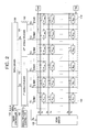
- the organic electroluminescent display device includes a display region 10, a scan driver 20, a data driver 30, and a timing controller 40.
- the display region 10 includes a plurality of pixels P11-Pnm formed at regions where a plurality of scan lines S1-Sn, a plurality of emission control lines E1-En, and a plurality of data lines D1-Dm cross.
- Each of the pixels P11-Pnm receives a first power supply voltage Vdd and a second power supply voltage Vss from one or more external power supplies, and emits light corresponding to a data signal transmitted from the data lines D1-Dm, thereby displaying an image. Further, an emission time of each of the pixels P11- Pnm is controlled according to one or more emission control signals transmitted through the emission control lines E1-En.
- the scan driver 20 generates scan signals in response to a scan control signal Sg from the timing controller 40, and sequentially supplies the generated scan signals to the scan lines S1-Sn to select the pixels P11-Pnm. Further, the scan driver 20 generates emission control signals in response to the scan control signal Sg, and sequentially supplies the generated emission control signals to the emission control lines E1-En to control the emission.
- the data driver 30 receives R, G, and B data from the timing controller 40, generates one or more data signals in response to a data control signal Sd, and supplies the generated data signals to the data lines D1-Dm.
- the data driver 30 supplies the data signals to the data lines D1-Dm for one horizontal line per one horizontal period.
- the timing controller 40 generates the data control signal Sd in accordance with video data and the scan control signal Sg in accordance with horizontal and vertical synchronization signals Hsync and Vsync.
- the video data and/or the horizontal and vertical synchronization signals Hsync and Vsync are supplied from an external graphic controller (not shown).
- the data control signal Sd generated from the timing controller 40 is supplied to the data driver 30, and the scan control signal Sg is supplied from the timing controller 40 to the scan driver 20.
- the pixels P11-Pnm are disposed in the regions around where the scan lines S1-Sn, the emission control lines, E1-En, and the data lines D1-Dm cross (or intersect).
- the data driver 30 includes m output lines so as to supply the data signals to m data lines D1-Dm, respectively. That is, the data driver 30 in the conventional organic electroluminescent display device should have the same number of output lines as there are data lines D1-Dm. Therefore, the data driver 30 has to include a plurality of data integrated circuits (ICs) to form m output lines, thereby increasing production costs.
- ICs data integrated circuits
- the data ICs of the data driver 30 also increase. Therefore, production cost increases correspondingly. Therefore it is an object of the invention to provide an organic electroluminescent display device that allows for an increased display resolution while maintaining low production cost.
- An aspect of the present invention provides an organic electroluminescent display device that employs a demultiplexer to reduce the number of output lines of a data driver and display an image with uniform brightness.
- an organic electroluminescent display device includes:
- the storage capacitor has a capacitance which is at least five times larger than the capacitance of the auxiliary capacitor. Still more preferably, the storage capacitor has a capacitance which is at least five times larger than the capacitance of the auxiliary capacitor.
- an organic electroluminescent display device includes a plurality of pixels formed at regions where a plurality of scan lines and a plurality of data lines cross.
- Each of the pixels includes: a pixel driving circuit comprising a storage capacitor for storing a data voltage from at least one of the data lines in response to a scan signal of at least one of the scan lines and an auxiliary capacitor connected between the storage capacitor and the at least one of the scan lines to generate a compensation voltage for increasing the data voltage according to a level change of the scan signal, and being adapted to output a driving current; and an organic light emitting diode connected to the pixel driving circuit to emit light with a brightness according to an amount of the driving current.
- the storage capacitor has a capacitance which is at least five times larger than the capacitance of the auxiliary capacitor. Still more preferably, the storage capacitor has a capacitance which is at least five times larger than the capacitance of the auxiliary capacitor.
- FIG. 2 is a block diagram of an organic electroluminescent display device according to an embodiment of the present invention.
- the organic electroluminescent display device includes a display region 100, a scan driver 120, a data driver 130, a timing controller 140, a demultiplexing unit 150, and a demultiplexer controller 160.
- the display region 100 includes a plurality of pixels P111-Pnmk disposed at regions defined by a plurality of scan lines S1-Sn, a plurality of emission control lines E1-En, and a plurality of data lines D11-Dmk.
- Each of the pixels P111-Pnmk emits light corresponding to a data signal transmitted from the data lines D11-Dmk.
- An exemplary pixel 110 among the pixels P111-Pnmk will be described below in more detail.
- a plurality of data line capacitors C data11 -C datamk are provided corresponding to the respective data lines D11-Dmk to thereby temporarily store the data signals.
- the 1 st data line capacitor C data11 formed in the data line D11 temporarily stores the data voltage. Then, in a scan period, when the 1 st pixel P111 is selected by the 1st scan signal S1, the data voltage stored in the 1 st data line capacitor C data11 is supplied to the 1 st pixel P111 so that light is emitted corresponding to the data voltage.
- the data line capacitors C data11 -C datamk formed in the respective data lines D11-Dmk temporarily store the data signals supplied to the plurality of data lines D11-Dmk, and supply the stored data voltages to the pixels P111-Pnmk selected by the scan signals.
- the data line capacitors C data11 -C datamk can be realized by parasitic capacitances (or capacitors) equivalently formed by the data lines D11-Dmk, a third electrode, and an insulating layer therebetween.
- the capacitance of each of the data line capacitors C data11 -C datamk is set to be larger than that of a storage capacitor Cst provided in each of the pixels P111-Pnmk to stably store the data signals.
- the scan driver 120 generates scan signals in response to a scan control signal Sg supplied from the timing controller 140, and sequentially supplies the generated scan signals to the scan lines S1-Sn.
- the scan driver 110 supplies the scan signal only in a partial period (i.e., a scan period) of one horizontal period 1 H.
- one horizontal period 1 H is divided into a scan period and a data programming period.
- the scan driver 120 supplies the scan signal to the scan line Sn in the scan period of one horizontal period 1 H, and does not supply the scan signal in the data programming period.
- the scan driver 120 generates emission control signals in response to the scan control signal Sg, and sequentially supplies the emission control signals to the emission control lines E1-En, thereby controlling the emission.
- the data driver 130 receives R, G and B data from the timing controller 140, and sequentially supplies the R, G and B data signals to output lines D1-Dm in response to data control signals Sd.
- the data driver 130 sequentially supplies k data signals (e.g., three R, G and B data signals in FIG. 7) to the output lines D1-Dm connected to respective output terminals thereof, in which k is an integer greater than or equal to 2.
- the data driver 130 sequentially supplies data signals (e.g., R, G and B data) to the corresponding pixels in the data programming period of one horizontal period 1H.
- the data signals (R, G and B) are supplied only in the data programming period, which does not overlap the scan period for supplying the scan signal.
- the timing controller 140 generates the data control signal Sd in accordance with video data and the scan control signal Sg in accordance with horizontal and vertical synchronization signals Hsync and Vsync.
- the video data and/or the horizontal and vertical synchronization signals Hsync and Vsync are supplied from one or more external graphic controllers (not shown).
- the data control signal Sd generated from the timing controller 140 is supplied to the data driver 130, and the scan control signal Sg is supplied from the timing controller 140 to the scan driver 120.
- the demultiplexing unit 150 includes m demultiplexers 151.
- the demultiplexing unit 150 includes the same number of demultiplexers 151 as the number of output lines D1-Dm connected to the data driver 130, and input terminals of the demultiplexers 151 are connected to the output lines D1-Dm of the data driver 130, respectively. Further, an output terminal of each of the demultiplexers 151, e.g., the output terminal of the 1 st demultiplexer 151, is connected to k data lines D11-D1k.
- the 1 st demultiplexer 151 applies k data signals, sequentially supplied in the data programming period, to the k data lines D11-D1k.
- the number of output lines that are needed in the data driver 130 can be decreased. For example, assuming that k is 3, the number of output lines provided in the data driver 130 decreases to one third (1/3) of the number of output lines in a conventional data driver.
- the number of data ICs provided in the data driver 130 can also be decreased to one third (1/3) of the number of the conventional data driver.
- the demultiplexer (or 1st demultiplexer) 151 when used to supply the data signals from one output line D1 to the k data lines D11-D1k, the production cost of the data ICs can be reduced.
- the demultiplexer controller 160 supplies the k control signals to control terminals of the demultiplexer 151 in the data programming period of one horizontal period 1 H so that the demultiplexer 151 can individually supply the k data signals of the output line D1 to the k data lines D11-D1k.
- the k control signals e.g., CS1, CS2, and CS3 are sequentially supplied from the demultiplexer controller 160 in the data programming period without overlapping one another.
- the demultiplexer controller 160 is provided separately from the timing controller 140 (refer to FIG. 2), but the invention is not limited to such a configuration. E.g. the demultiplexer controller 160 may be provided integrally with the timing controller 140.
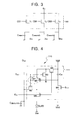
- FIG. 3 is a circuit diagram of the demultiplexer of FIG. 2.
- k 3
- the data voltages are input in order of red, green and blue.
- the demultiplexer 151 is connected to the 1 st output line D1 of the data driver 130.
- the demultiplexer 151 includes a first switching device T1, a second switching device T2, and a third switching device T3.
- each of the switching devices T1, T2, and T3 can be formed by a thin film transistor.
- the switching devices T1, T2 and T3 are implemented by P-type metal oxide semiconductor field effect transistors (MOSFETs), but the invention is not limited to using P-type MOSFETs.
- the invention is not limited to a conductive type of the transistors (i.e., the invention is not limited to a type of major carriers in the channels (or channel type) of the transistors).
- the switching devices T1, T2 and T3 may be implemented by N-type MOSFETs.
- the first switching device T1 is connected between the 1 st output line D1 and the 1 st data line D11.
- the first switching device T1 is turned on when a 1 st control signal CS1 is supplied from the demultiplexer controller 160, and supplies a red data signal from the 1 st output line D1 to the 1 st data line D11.
- the data signal supplied to the 1 st data line D11 is stored in the 1 st data line capacitor C data11 in the data programming period shown in FIG. 7.
- the second switching device T2 is connected between the 1 st output line D1 and the 2 nd data line D12.
- the second switching device T2 is turned on when a 2 nd control signal CS2 is supplied from the demultiplexer controller 160, and supplies a green data signal from the 1 st output line D1 to the 2 nd data line D12.
- the data signal supplied to the 2 nd data line D12 is stored in the 2 nd data line capacitor C data12 in the data programming period shown in FIG. 7.
- the third switching device T3 is connected between the 1 st output line D1 and the 3 rd data line D13.
- the third switching device T3 is turned on when a 3 rd control signal CS3 is supplied from the demultiplexer controller 160, and supplies a blue data signal from the 1 st output line D1 to the 3 rd data line D13.
- the data signal supplied to the 3 rd data line D13 is stored in the 3 rd data line capacitor C data13 in the data programming period shown in FIG. 7.
- Such operations of the demultiplexer 151 will be described later in more detail and in association with the structure of the pixel 110.
- FIG. 4 is a circuit diagram of an exemplary pixel among n*m*k pixels of FIG. 2, but the present invention is not limited to the illustrated circuit configuration.
- the exemplary pixel 110 includes a pixel driving circuit 111 that is connected to an organic light emitting diode OLED, a data line Dmk, previous and current scan lines Sn and Sn-1, an emission control line En, a first power supply voltage line of a first power supply voltage Vdd, and an initialization voltage line Vinit, and generates a driving current to make the organic light emitting diode OLED emit light.
- the data line Dmk is formed with a data line capacitor C datamk to supply a data voltage to the pixel 110.
- the organic light emitting diode OLED has an anode connected to the pixel driving circuit 111, and a cathode connected to a second power supply voltage line of a second power supply voltage Vss.
- the second power supply voltage Vss is lower in voltage level than the first power supply voltage Vdd.
- the second power supply voltage Vss may be a ground voltage, a negative voltage, etc.
- the organic light emitting diode (OLED) emits light corresponding to the driving current supplied from the pixel driving circuit 111.
- the pixel driving circuit 111 has a threshold voltage compensation circuit and includes a storage capacitor Cst and six transistors M1, M2, M3, M4, M5, and M6.
- the first transistor M1 is a driving transistor.
- the third transistor M3 is a threshold voltage compensation transistor for compensating a threshold voltage by connecting the first (or driving) transistor M1 to function like a diode.
- the fourth transistor M4 is an initialization transistor for initializing the storage capacitor Cst.
- the sixth transistor M6 is an emission control transistor for controlling emission of the organic light emitting diode OLED.
- the second and fifth transistors M2 and M5 are first and second switching transistors.
- the first switching transistor M2 has a gate electrode connected to the scan line Sn, and a source electrode connected to the data line Dmk.
- the first switching transistor M2 is turned on by the scan signal transmitted through the current scan line Sn, and applies the data voltage from the data line capacitor C datamk to a node N.
- the driving transistor M1 has a first electrode (e.g., a drain electrode) connected to a drain electrode of the first switching transistor M2, and a gate electrode connected to the node N.
- a source or drain electrode of the threshold voltage compensation transistor M3, and a first terminal of the storage capacitor Cst are connected in common to the node N.
- the threshold voltage compensation transistor M3 is connected between the gate electrode and a second electrode (e.g., a source electrode) of the driving transistor M1, and connects the driving transistor M1 to function like a diode in response to the scan signal transmitted through the current scan line Sn.
- the driving transistor M1 operates substantially as a diode according to the scan signal, so that a voltage Vdata - Vth [V] is applied to the node N and used as the gate voltage of the driving transistor M1.
- the driving transistor M1 generates the driving current corresponding to a voltage applied to the gate electrode thereof.
- the initialization transistor M4 is connected between the initialization voltage line Vinit and the first terminal of the storage capacitor Cst, and discharges an electric charge, which is charged in the storage capacitor Cst in a previous frame, through the initialization voltage line Vinit in response to the scan signal of the previous scan line Sn-1 connected to a gate electrode of the initialization transistor M4.
- the initialization transistor M4 initializes the storage capacitor Cst.
- the second switching transistor M5 is connected between the first power supply voltage line of the first power supply voltage Vdd and the second (or source) electrode of the driving transistor M1.
- the second switching transistor M5 is turned on by the emission control signal transmitted through the emission control line En connected to the gate electrode thereof, and supplies the first power supply voltage Vdd to the source electrode of the driving transistor M1.
- the emission control transistor M6 is connected between the driving transistor M1 and the organic light emitting diode OLED, and applies the driving current generated by the driving transistor M1 to the organic light emitting diode OLED in response to the emission control signal transmitted through the emission control line En connected to a gate electrode of the emission control transistor M6.
- the storage capacitor Cst is connected between the first power supply voltage line Vdd and the gate electrode of the driving transistor M1, and maintains an electric charge corresponding to a voltage difference between the first power supply voltage Vdd and the voltage Vdata - Vth[V] applied to the gate electrode of the driving transistor M1 during one frame.
- the first through sixth transistors M1 through M6 are PMOSFETs, but the invention is not limited to such a configuration.
- the invention is not limited to a conductive type of the transistors (i.e., the invention is not limited to a type of major carriers in the channels (or channel type) of the transistors). That is, the first through sixth transistors may be implemented as NMOSFETs for example.
- the data line capacitor C datamk stores a voltage corresponding to the data signal in the data programming period, and supplies the voltage stored in the data line capacitor C datamk to the pixel in the scan period, thereby supplying the data signal to the pixel.
- the voltages stored in the data line capacitors C data11 -C data1k are supplied to the respective pixels at the same time. That is, because the respective data signals are supplied at the same time, an image can be displayed with uniform brightness.
- Vg M1 is a gate voltage of the driving transistor M1
- Vdata is a data voltage
- Vinit is an initialization voltage
- Vdd is a first power supply voltage
- Cdata is a capacitor of each data line
- Cst is a storage capacitor of each pixel.
- the gate voltage Vg M1 of the driving transistor M1 differs from the data voltage Vdata according to the capacitances of the data line capacitor Cdata and the storage capacitor Cst in the pixel. That is, a lower voltage than the data voltage applied to the data line is actually applied to the gate electrode of the driving transistor. Therefore, it is difficult to properly represent a black gradation, thereby deteriorating a contrast ratio.
- This problem can be solved by increasing the black data voltage. However, it is difficult or impossible to increase the back data voltage without changing a specification of the data driver. Alternatively, this problem can be solved by lowering the first power supply voltage Vdd. In this case, the black gradation can be properly represented if the second power supply voltage Vss is also lowered to as much as the voltage level of the first power supply voltage Vdd has been lowered. As such, a DC/DC efficiency of the power supply voltages Vdd and Vss may also be lowered.
- an auxiliary capacitor Caux is formed in a pixel as shown in FIG. 4.
- the pixel according to an embodiment of the present invention further includes an auxiliary capacitor Caux.
- the auxiliary capacitor Caux has a first terminal connected in common to the current scan line Sn and the gate electrode of the first switching transistor M2, and a second terminal connected in common to the storage capacitor Cst and the gate electrode of the driving transistor M1.
- the auxiliary capacitor Caux is employed to boost up the gate voltage V G of the driving transistor M1 during a change from a scan period to an emission period.
- low and high level voltages of a scan signal are referred to as a low scan voltage (or signal) VVSS and a high scan voltage (or signal) VVDD, respectively.
- VVSS low scan voltage
- VVDD high scan voltage
- the gate voltage V G of the driving transistor M1 is boosted up to as much as a compensation voltage obtained by coupling the storage capacitor Cst to the auxiliary capacitor Caux.
- VVDD is a high level scan voltage (or signal)
- VVSS is a low level scan voltage (or signal)
- Vg M1 is a voltage applied to the gate electrode of the driving transistor M1 when the low level scan voltage (or signal) VVSS is applied
- V G is a voltage applied to the gate electrode of the driving transistor M1 when the high level scan voltage (or signal) VVSS is applied
- Caux is a capacitance of an auxiliary capacitor
- Cst is a capacitance of a storage capacitor.
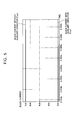
- Equation 2 as the auxiliary capacitor Caux is added to the pixel, the voltage applied to the gate electrode of the driving transistor M1 is increased to as much as a compensation voltage of Caux*(VVDD-VVSS)/(Cst+Caux), thereby compensating for the voltage difference. Therefore, a black current flow is substantially reduced while the black level gradation voltage is applied, thereby enhancing the contrast ratio. This is shown in the graph of FIG. 5.
- FIG. 5 is a graph of a simulation of black current flowing when a black gradation voltage is applied to the pixel of FIG. 4.
- a first power supply voltage Vdd of 5V, a second power supply voltage Vss of -6V, and a data voltage Vdata of 5V are applied to the pixel shown in FIG. 4. Further, in FIG. 5, a vertical axis indicates the amount of black current, and a horizontal axis indicates time.
- the first power supply voltage Vdd is equal to the black data voltage
- a high black current of about 7nA flows in the driving transistor M1 in the pixel without the auxiliary capacitor Caux, and thus the contrast ratio is very low.
- a low black current of about 0.02nA flows in the driving transistor M1in the pixel with the auxiliary capacitor Caux according to an embodiment of the present invention, thereby satisfying the specification of 0.03nA and enhancing the contrast ratio.
- the auxiliary capacitor Caux is formed in the pixel, so that the lowering of the data voltage applied to the pixel is prevented or substantially reduced. As such, in the pixel with the auxiliary capacitor Caux, it is not necessary to lower the first and second power supply voltages Vdd and Vss, thereby enhancing DC/DC efficiency.
- the capacitance of the storage capacitor Cst is larger than that of the auxiliary capacitor Caux.
- the capacitance of the storage capacitor Cst is larger than that of the auxiliary capacitor Caux by about ten times.
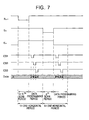
- FIG. 6 is a circuit diagram illustrating a detailed connection structure between the demultiplexer of FIG. 3 and the pixel of FIG. 4 according to an embodiment of the present invention
- FIG. 7 is a timing diagram for driving a pixel circuit of FIG. 6.
- a low level scan signal is supplied to the (n-1) th scan line Sn-1 in the (n-1) th scan period of one horizontal period 1 H.
- each initialization transistor M4 of the R, G and B sub-pixels is turned on.
- the initialization transistor M4 is turned on, the first terminal of the storage capacitor Cst and the gate electrode of the driving transistor M1 are connected to the initialization power supply line Vinit.
- the scan signal is supplied to the (n-1) th scan line Sn-1
- the previous frame data voltage stored in each storage capacitor Cst of the R, G and B pixels i.e., the gate voltage of the driving transistor M1
- the scan signal is supplied to the (n-1) th scan line Sn-1
- the first switching transistor M2 connected to the n th scan line Sn is maintained in an off state.
- the first switching device T1, the second switching device T2, and the third switching device T3 are sequentially turned on by the first through third control signals CS1, CS2 and CS3 sequentially supplied in the data programming period.
- the first switching device T1 is turned on by the first control signal CS1
- the R data signal is supplied from the 1 st output line D1 to the 1 st data line D11.
- the 1 st data line capacitor C data11 is charged with a voltage corresponding to the R data signal supplied to the 1 st data line D11.
- the second switching device T2 is turned on by the 2 nd control signal CS2
- the G data signal is supplied from the 1 st output line D1 to the 2 nd data line D12.
- the 2 nd data line capacitor C data12 is charged with a voltage corresponding to the G data signal supplied to the 2 nd data line D12.
- the B data signal is supplied from the 1 st output line D1 to the 3 rd data line D13.
- the 3 rd data line capacitor C data13 is charged with a voltage corresponding to the B data signal supplied to the 3 rd data line D13.
- the scan signal is not supplied to the n th scan line Sn in the data programming period, so that the R, G and B data signals are not supplied to the R, G and B pixels, respectively.
- a low level scan signal is supplied to the n th scan line Sn in the n th scan period following the data programming period.
- each first switching transistor M2 and each threshold voltage compensation transistor M3 provided in the R, G and B pixels are turned on.
- Each first switching transistor M2 of the R, G and B pixels transmits a voltage Vdata corresponding to each of the R, G and B data signals, which is stored in the 1 st through 3 rd data line capacitors C data11 through C data13 in the data programming period, to the respective R, G and B pixels.
- the threshold voltage compensation transistor M3 connects the driving transistor M1 to function like a diode.
- a voltage Vdata-Vth M1 [V] corresponding to a difference between the voltage Vdata corresponding to each of the R, G and B data signals stored in the 1 st through 3 rd data line capacitors C data11 through C data13 and the threshold voltage Vth of the corresponding driving transistor M1 is applied to both the gate electrode of the driving transistor M1 and the first terminal of the storage capacitor Cst through the driving transistor M1 connected to function like a diode.
- the voltage applied to the gate electrode of the driving transistor M1 is equal to the value obtained by Equation 1.
- the second switching transistor M5 and the emission control transistor M6 are turned on, so that the first power supply Vdd applied to the source electrode of the driving transistor M1 and the driving current corresponding to the voltage applied to the gate electrode thereof are supplied to the organic light emitting diode OLED through the emission control transistor M6, thereby emitting light with a certain (or predetermined) brightness.
- the voltage applied to the gate electrode of the driving transistor M1 is equal to the value obtained by Equation 2.
- the organic electroluminescent display device employs the demultiplexer 151 to sequentially supply R, G and B data signals from the 1 st output line D1 to k data lines D11-D1k. Further, voltages corresponding to the data signals are stored in the data line capacitors C data11 -C data1k in the data programming period, and the voltages stored in the data line capacitors C data11 -C data1k are supplied to the pixels in the scan period. Thus, the voltages stored in the data line capacitors C data11 -C data1k are supplied to the respective pixels at the same time, i.e., the data signals are supplied at the same time, thereby displaying an image with uniform brightness.
- auxiliary capacitor Caux in each pixel compensates for electric charge being shared between the data line capacitor Cdata and the storage capacitor Cst which substantially lowers the voltage applied to the pixel.
- the DC/DC efficiency is maintained without lowering the power supply voltages Vdd and Vss and the contrast ratio is enhanced.
- an embodiment of the present invention provides an organic electroluminescent display device in which an auxiliary capacitor Caux is formed in a pixel so that a data voltage applied to the pixel by a demultiplexer is compensated, thereby representing a black gradation and enhancing a contrast ratio.
Landscapes
- Engineering & Computer Science (AREA)
- Physics & Mathematics (AREA)
- Computer Hardware Design (AREA)
- General Physics & Mathematics (AREA)
- Theoretical Computer Science (AREA)
- Control Of El Displays (AREA)
- Control Of Indicators Other Than Cathode Ray Tubes (AREA)
- Electroluminescent Light Sources (AREA)
Abstract
Description
- The present invention relates to an organic electroluminescent display device, and more particularly, to an organic electroluminescent display device that employs a demultiplexer to reduce the number of output lines of a data driver and display an image with uniform brightness.
- An organic light emitting diode (OLED) of an organic electroluminescent display device is a self-emissive element that emits light by recombination of electrons supplied from a cathode and holes supplied from an anode. The organic electroluminescent display device employs a thin film transistor (TFT) formed in each pixel to supply a driving current corresponding to a data signal to the organic light emitting diode (OLED), thereby causing the organic light emitting diode (OLED) to emit light and display an image (or a predetermined image).
- FIG. 1 is a block diagram of a conventional organic electroluminescent display device.
- Referring to FIG. 1, the organic electroluminescent display device includes a
display region 10, ascan driver 20, adata driver 30, and atiming controller 40. - The
display region 10 includes a plurality of pixels P11-Pnm formed at regions where a plurality of scan lines S1-Sn, a plurality of emission control lines E1-En, and a plurality of data lines D1-Dm cross. Each of the pixels P11-Pnm receives a first power supply voltage Vdd and a second power supply voltage Vss from one or more external power supplies, and emits light corresponding to a data signal transmitted from the data lines D1-Dm, thereby displaying an image. Further, an emission time of each of the pixels P11- Pnm is controlled according to one or more emission control signals transmitted through the emission control lines E1-En. - The
scan driver 20 generates scan signals in response to a scan control signal Sg from thetiming controller 40, and sequentially supplies the generated scan signals to the scan lines S1-Sn to select the pixels P11-Pnm. Further, thescan driver 20 generates emission control signals in response to the scan control signal Sg, and sequentially supplies the generated emission control signals to the emission control lines E1-En to control the emission. - The
data driver 30 receives R, G, and B data from thetiming controller 40, generates one or more data signals in response to a data control signal Sd, and supplies the generated data signals to the data lines D1-Dm. Here, thedata driver 30 supplies the data signals to the data lines D1-Dm for one horizontal line per one horizontal period. - The
timing controller 40 generates the data control signal Sd in accordance with video data and the scan control signal Sg in accordance with horizontal and vertical synchronization signals Hsync and Vsync. The video data and/or the horizontal and vertical synchronization signals Hsync and Vsync are supplied from an external graphic controller (not shown). The data control signal Sd generated from thetiming controller 40 is supplied to thedata driver 30, and the scan control signal Sg is supplied from thetiming controller 40 to thescan driver 20. - In the conventional organic electroluminescent display device with this configuration, the pixels P11-Pnm are disposed in the regions around where the scan lines S1-Sn, the emission control lines, E1-En, and the data lines D1-Dm cross (or intersect). Here, the
data driver 30 includes m output lines so as to supply the data signals to m data lines D1-Dm, respectively. That is, thedata driver 30 in the conventional organic electroluminescent display device should have the same number of output lines as there are data lines D1-Dm. Therefore, thedata driver 30 has to include a plurality of data integrated circuits (ICs) to form m output lines, thereby increasing production costs. Particularly, as the resolution and the size of thedisplay region 10 increase, the data ICs of thedata driver 30 also increase. Therefore, production cost increases correspondingly. Therefore it is an object of the invention to provide an organic electroluminescent display device that allows for an increased display resolution while maintaining low production cost. - An aspect of the present invention provides an organic electroluminescent display device that employs a demultiplexer to reduce the number of output lines of a data driver and display an image with uniform brightness.
- According to an embodiment of the present invention, an organic electroluminescent display device includes:
- a display region having a plurality of pixels formed at regions where a plurality of scan lines and a plurality of data lines cross to display an image thereon; a scan driver being adapted to supply scan signals to the plurality of scan lines; and a data driver being adapted to supply data voltages to a plurality of output lines connected to a plurality of demultiplexers, the demultiplexers being adapted to sequentially supply the data voltages to the plurality of data lines. Each of the pixels includes: a storage capacitor being adapted to store one of the data voltages from one of the data lines in response to a first one of the scan signals; and an auxiliary capacitor connected between the storage capacitor and the one of the scan lines, the auxiliary capacitor being adapted to generate a compensation voltage according to a level change of the first one of the scan signals and to apply the compensation voltage to the one of the data voltages stored in the storage capacitor.
- Preferably the storage capacitor has a capacitance which is at least five times larger than the capacitance of the auxiliary capacitor. Still more preferably, the storage capacitor has a capacitance which is at least five times larger than the capacitance of the auxiliary capacitor.
- According to another embodiment of the present invention, an organic electroluminescent display device includes a plurality of pixels formed at regions where a plurality of scan lines and a plurality of data lines cross. Each of the pixels includes: a pixel driving circuit comprising a storage capacitor for storing a data voltage from at least one of the data lines in response to a scan signal of at least one of the scan lines and an auxiliary capacitor connected between the storage capacitor and the at least one of the scan lines to generate a compensation voltage for increasing the data voltage according to a level change of the scan signal, and being adapted to output a driving current; and an organic light emitting diode connected to the pixel driving circuit to emit light with a brightness according to an amount of the driving current.
- Preferably the storage capacitor has a capacitance which is at least five times larger than the capacitance of the auxiliary capacitor. Still more preferably, the storage capacitor has a capacitance which is at least five times larger than the capacitance of the auxiliary capacitor.
- The accompanying drawings, together with the specification, illustrate exemplary embodiments of the present invention, and, together with the description, serve to explain the principles of the present invention.
- FIG. 1 is a block diagram of a conventional organic electroluminescent display device;
- FIG. 2 is a block diagram of an organic electroluminescent display device according to an embodiment of the present invention;
- FIG. 3 is a circuit diagram of a demultiplexer of FIG. 2;
- FIG. 4 is a circuit diagram of an exemplary pixel among N×M pixels of FIG. 2;
- FIG. 5 is a graph of a simulation of black current flowing when a black gradation voltage is applied to the pixel of FIG. 4;
- FIG. 6 is a circuit diagram illustrating a detailed connection structure between the demultiplexer of FIG. 3 and the pixel of FIG. 4 according to an embodiment of the present invention; and
- FIG. 7 is a timing diagram for driving a pixel circuit of FIG. 6.
- FIG. 2 is a block diagram of an organic electroluminescent display device according to an embodiment of the present invention.
- Referring to FIG. 2, the organic electroluminescent display device according to an embodiment of the present invention includes a
display region 100, ascan driver 120, adata driver 130, atiming controller 140, ademultiplexing unit 150, and ademultiplexer controller 160. - The
display region 100 includes a plurality of pixels P111-Pnmk disposed at regions defined by a plurality of scan lines S1-Sn, a plurality of emission control lines E1-En, and a plurality of data lines D11-Dmk. - Each of the pixels P111-Pnmk emits light corresponding to a data signal transmitted from the data lines D11-Dmk. An
exemplary pixel 110 among the pixels P111-Pnmk will be described below in more detail. - In the regions of the pixels P111-Pnmk, a plurality of data line capacitors Cdata11-Cdatamk are provided corresponding to the respective data lines D11-Dmk to thereby temporarily store the data signals.
- For example, in a data programming period, when a data voltage is applied to the 1st data line D11 so as to make the 1st pixel P111 emit light, the 1st data line capacitor Cdata11 formed in the data line D11 temporarily stores the data voltage. Then, in a scan period, when the 1st pixel P111 is selected by the 1st scan signal S1, the data voltage stored in the 1st data line capacitor Cdata11 is supplied to the 1st pixel P111 so that light is emitted corresponding to the data voltage.
- Thus, the data line capacitors Cdata11-Cdatamk formed in the respective data lines D11-Dmk temporarily store the data signals supplied to the plurality of data lines D11-Dmk, and supply the stored data voltages to the pixels P111-Pnmk selected by the scan signals. Here, the data line capacitors Cdata11-Cdatamk can be realized by parasitic capacitances (or capacitors) equivalently formed by the data lines D11-Dmk, a third electrode, and an insulating layer therebetween. Here, substantially, the capacitance of each of the data line capacitors Cdata11-Cdatamk is set to be larger than that of a storage capacitor Cst provided in each of the pixels P111-Pnmk to stably store the data signals.
- The
scan driver 120 generates scan signals in response to a scan control signal Sg supplied from thetiming controller 140, and sequentially supplies the generated scan signals to the scan lines S1-Sn. Here, as shown in FIG. 7, thescan driver 110 supplies the scan signal only in a partial period (i.e., a scan period) of onehorizontal period 1 H. - In more detail, one
horizontal period 1 H according to an embodiment of the present invention is divided into a scan period and a data programming period. Thescan driver 120 supplies the scan signal to the scan line Sn in the scan period of onehorizontal period 1 H, and does not supply the scan signal in the data programming period. In addition, thescan driver 120 generates emission control signals in response to the scan control signal Sg, and sequentially supplies the emission control signals to the emission control lines E1-En, thereby controlling the emission. - The
data driver 130 receives R, G and B data from thetiming controller 140, and sequentially supplies the R, G and B data signals to output lines D1-Dm in response to data control signals Sd. Here, thedata driver 130 sequentially supplies k data signals (e.g., three R, G and B data signals in FIG. 7) to the output lines D1-Dm connected to respective output terminals thereof, in which k is an integer greater than or equal to 2. In more detail, thedata driver 130 sequentially supplies data signals (e.g., R, G and B data) to the corresponding pixels in the data programming period of onehorizontal period 1H. Here, the data signals (R, G and B) are supplied only in the data programming period, which does not overlap the scan period for supplying the scan signal. - The
timing controller 140 generates the data control signal Sd in accordance with video data and the scan control signal Sg in accordance with horizontal and vertical synchronization signals Hsync and Vsync. The video data and/or the horizontal and vertical synchronization signals Hsync and Vsync are supplied from one or more external graphic controllers (not shown). The data control signal Sd generated from thetiming controller 140 is supplied to thedata driver 130, and the scan control signal Sg is supplied from thetiming controller 140 to thescan driver 120. - The
demultiplexing unit 150 includesm demultiplexers 151. In more detail, thedemultiplexing unit 150 includes the same number ofdemultiplexers 151 as the number of output lines D1-Dm connected to thedata driver 130, and input terminals of thedemultiplexers 151 are connected to the output lines D1-Dm of thedata driver 130, respectively. Further, an output terminal of each of thedemultiplexers 151, e.g., the output terminal of the 1st demultiplexer 151, is connected to k data lines D11-D1k. The 1st demultiplexer 151 (hereafter also referred to as the demultiplexer 151) applies k data signals, sequentially supplied in the data programming period, to the k data lines D11-D1k. Thus, when the k data signals sequentially supplied to a single output line D1 are sequentially applied to the k data lines D11-D1k, the number of output lines that are needed in thedata driver 130 can be decreased. For example, assuming that k is 3, the number of output lines provided in thedata driver 130 decreases to one third (1/3) of the number of output lines in a conventional data driver. In addition, the number of data ICs provided in thedata driver 130 can also be decreased to one third (1/3) of the number of the conventional data driver. Thus, according to an embodiment of the present invention, when the demultiplexer (or 1st demultiplexer) 151 is used to supply the data signals from one output line D1 to the k data lines D11-D1k, the production cost of the data ICs can be reduced. - The
demultiplexer controller 160 supplies the k control signals to control terminals of thedemultiplexer 151 in the data programming period of onehorizontal period 1 H so that thedemultiplexer 151 can individually supply the k data signals of the output line D1 to the k data lines D11-D1k. Here, as shown in FIG. 7, the k control signals (e.g., CS1, CS2, and CS3) are sequentially supplied from thedemultiplexer controller 160 in the data programming period without overlapping one another. In this embodiment, thedemultiplexer controller 160 is provided separately from the timing controller 140 (refer to FIG. 2), but the invention is not limited to such a configuration. E.g. thedemultiplexer controller 160 may be provided integrally with thetiming controller 140. - FIG. 3 is a circuit diagram of the demultiplexer of FIG. 2.
- For convenience purposes, in FIG. 3, it is assumed that k is 3, and the data voltages are input in order of red, green and blue. Further, it is assumed that the
demultiplexer 151 is connected to the 1st output line D1 of thedata driver 130. - Referring to FIG. 3, the
demultiplexer 151 includes a first switching device T1, a second switching device T2, and a third switching device T3. Here, each of the switching devices T1, T2, and T3 can be formed by a thin film transistor. According to an embodiment of the present invention, the switching devices T1, T2 and T3 are implemented by P-type metal oxide semiconductor field effect transistors (MOSFETs), but the invention is not limited to using P-type MOSFETs. In addition, the invention is not limited to a conductive type of the transistors (i.e., the invention is not limited to a type of major carriers in the channels (or channel type) of the transistors). For example, the switching devices T1, T2 and T3 may be implemented by N-type MOSFETs. - The first switching device T1 is connected between the 1st output line D1 and the 1st data line D11. The first switching device T1 is turned on when a 1st control signal CS1 is supplied from the
demultiplexer controller 160, and supplies a red data signal from the 1st output line D1 to the 1st data line D11. The data signal supplied to the 1st data line D11 is stored in the 1st data line capacitor Cdata11 in the data programming period shown in FIG. 7. - The second switching device T2 is connected between the 1st output line D1 and the 2nd data line D12. The second switching device T2 is turned on when a 2nd control signal CS2 is supplied from the
demultiplexer controller 160, and supplies a green data signal from the 1st output line D1 to the 2nd data line D12. The data signal supplied to the 2nd data line D12 is stored in the 2nd data line capacitor Cdata12 in the data programming period shown in FIG. 7. - The third switching device T3 is connected between the 1st output line D1 and the 3rd data line D13. The third switching device T3 is turned on when a 3rd control signal CS3 is supplied from the
demultiplexer controller 160, and supplies a blue data signal from the 1st output line D1 to the 3rd data line D13. The data signal supplied to the 3rd data line D13 is stored in the 3rd data line capacitor Cdata13 in the data programming period shown in FIG. 7. Such operations of thedemultiplexer 151 will be described later in more detail and in association with the structure of thepixel 110. - FIG. 4 is a circuit diagram of an exemplary pixel among n*m*k pixels of FIG. 2, but the present invention is not limited to the illustrated circuit configuration.
- Referring to FIG. 4, the
exemplary pixel 110 according to an embodiment of the present invention includes apixel driving circuit 111 that is connected to an organic light emitting diode OLED, a data line Dmk, previous and current scan lines Sn and Sn-1, an emission control line En, a first power supply voltage line of a first power supply voltage Vdd, and an initialization voltage line Vinit, and generates a driving current to make the organic light emitting diode OLED emit light. The data line Dmk is formed with a data line capacitor Cdatamk to supply a data voltage to thepixel 110. - The organic light emitting diode OLED has an anode connected to the
pixel driving circuit 111, and a cathode connected to a second power supply voltage line of a second power supply voltage Vss. The second power supply voltage Vss is lower in voltage level than the first power supply voltage Vdd. For example, the second power supply voltage Vss may be a ground voltage, a negative voltage, etc. Thus, the organic light emitting diode (OLED) emits light corresponding to the driving current supplied from thepixel driving circuit 111. - The
pixel driving circuit 111 has a threshold voltage compensation circuit and includes a storage capacitor Cst and six transistors M1, M2, M3, M4, M5, and M6. Here, the first transistor M1 is a driving transistor. The third transistor M3 is a threshold voltage compensation transistor for compensating a threshold voltage by connecting the first (or driving) transistor M1 to function like a diode. The fourth transistor M4 is an initialization transistor for initializing the storage capacitor Cst. The sixth transistor M6 is an emission control transistor for controlling emission of the organic light emitting diode OLED. The second and fifth transistors M2 and M5 are first and second switching transistors. - The first switching transistor M2 has a gate electrode connected to the scan line Sn, and a source electrode connected to the data line Dmk. The first switching transistor M2 is turned on by the scan signal transmitted through the current scan line Sn, and applies the data voltage from the data line capacitor Cdatamk to a node N.
- The driving transistor M1 has a first electrode (e.g., a drain electrode) connected to a drain electrode of the first switching transistor M2, and a gate electrode connected to the node N. A source or drain electrode of the threshold voltage compensation transistor M3, and a first terminal of the storage capacitor Cst are connected in common to the node N.
- The threshold voltage compensation transistor M3 is connected between the gate electrode and a second electrode (e.g., a source electrode) of the driving transistor M1, and connects the driving transistor M1 to function like a diode in response to the scan signal transmitted through the current scan line Sn. Thus, the driving transistor M1 operates substantially as a diode according to the scan signal, so that a voltage Vdata - Vth [V] is applied to the node N and used as the gate voltage of the driving transistor M1. Thus, the driving transistor M1 generates the driving current corresponding to a voltage applied to the gate electrode thereof.
- The initialization transistor M4 is connected between the initialization voltage line Vinit and the first terminal of the storage capacitor Cst, and discharges an electric charge, which is charged in the storage capacitor Cst in a previous frame, through the initialization voltage line Vinit in response to the scan signal of the previous scan line Sn-1 connected to a gate electrode of the initialization transistor M4. Thus, the initialization transistor M4 initializes the storage capacitor Cst.
- The second switching transistor M5 is connected between the first power supply voltage line of the first power supply voltage Vdd and the second (or source) electrode of the driving transistor M1. The second switching transistor M5 is turned on by the emission control signal transmitted through the emission control line En connected to the gate electrode thereof, and supplies the first power supply voltage Vdd to the source electrode of the driving transistor M1.
- The emission control transistor M6 is connected between the driving transistor M1 and the organic light emitting diode OLED, and applies the driving current generated by the driving transistor M1 to the organic light emitting diode OLED in response to the emission control signal transmitted through the emission control line En connected to a gate electrode of the emission control transistor M6.
- The storage capacitor Cst is connected between the first power supply voltage line Vdd and the gate electrode of the driving transistor M1, and maintains an electric charge corresponding to a voltage difference between the first power supply voltage Vdd and the voltage Vdata - Vth[V] applied to the gate electrode of the driving transistor M1 during one frame.
- In FIG. 4, the first through sixth transistors M1 through M6 are PMOSFETs, but the invention is not limited to such a configuration. For example, the invention is not limited to a conductive type of the transistors (i.e., the invention is not limited to a type of major carriers in the channels (or channel type) of the transistors). That is, the first through sixth transistors may be implemented as NMOSFETs for example.
- In a pixel with this configuration, the data line capacitor Cdatamk stores a voltage corresponding to the data signal in the data programming period, and supplies the voltage stored in the data line capacitor Cdatamk to the pixel in the scan period, thereby supplying the data signal to the pixel. Thus, the voltages stored in the data line capacitors Cdata11-Cdata1k are supplied to the respective pixels at the same time. That is, because the respective data signals are supplied at the same time, an image can be displayed with uniform brightness.
- However, as the data programming period and the scan period are temporally separated in the pixel with this configuration, the data line capacitor Cdatamk and the storage capacitor Cst of the pixel, which are temporally separated in the data programming period, are temporally connected in the scan period, so that the electric charge corresponding to the data voltage Vdata stored in the data line capacitor Cdatamk is shared between the data line capacitor Cdatamk and the storage capacitor Cst. Thus, the gate voltage VgM1 of the driving transistor M1 is obtained by the following Equation 1:

- Here, VgM1 is a gate voltage of the driving transistor M1, Vdata is a data voltage, Vinit is an initialization voltage, Vdd is a first power supply voltage, Cdata is a capacitor of each data line, and Cst is a storage capacitor of each pixel.
- Referring to
Equation 1, the gate voltage VgM1 of the driving transistor M1 differs from the data voltage Vdata according to the capacitances of the data line capacitor Cdata and the storage capacitor Cst in the pixel. That is, a lower voltage than the data voltage applied to the data line is actually applied to the gate electrode of the driving transistor. Therefore, it is difficult to properly represent a black gradation, thereby deteriorating a contrast ratio. - This problem can be solved by increasing the black data voltage. However, it is difficult or impossible to increase the back data voltage without changing a specification of the data driver. Alternatively, this problem can be solved by lowering the first power supply voltage Vdd. In this case, the black gradation can be properly represented if the second power supply voltage Vss is also lowered to as much as the voltage level of the first power supply voltage Vdd has been lowered. As such, a DC/DC efficiency of the power supply voltages Vdd and Vss may also be lowered.
- According to an embodiment of the present invention, an auxiliary capacitor Caux is formed in a pixel as shown in FIG. 4.
- That is, the pixel according to an embodiment of the present invention further includes an auxiliary capacitor Caux.
- The auxiliary capacitor Caux has a first terminal connected in common to the current scan line Sn and the gate electrode of the first switching transistor M2, and a second terminal connected in common to the storage capacitor Cst and the gate electrode of the driving transistor M1.
- The auxiliary capacitor Caux is employed to boost up the gate voltage VG of the driving transistor M1 during a change from a scan period to an emission period. Here, low and high level voltages of a scan signal are referred to as a low scan voltage (or signal) VVSS and a high scan voltage (or signal) VVDD, respectively. Thus, when a voltage applied to the first terminal of the auxiliary capacitor Caux changes from the low scan voltage VVSS to the high scan voltage VVDD, the gate voltage VG of the driving transistor M1 is boosted up to as much as a compensation voltage obtained by coupling the storage capacitor Cst to the auxiliary capacitor Caux.
- The gate voltage VG of the driving transistor M1 can be obtained by the following Equation 2:


- Here, VVDD is a high level scan voltage (or signal), VVSS is a low level scan voltage (or signal), VgM1 is a voltage applied to the gate electrode of the driving transistor M1 when the low level scan voltage (or signal) VVSS is applied, VG is a voltage applied to the gate electrode of the driving transistor M1 when the high level scan voltage (or signal) VVSS is applied, Caux is a capacitance of an auxiliary capacitor, and Cst is a capacitance of a storage capacitor.
- Referring to Equation 2, as the auxiliary capacitor Caux is added to the pixel, the voltage applied to the gate electrode of the driving transistor M1 is increased to as much as a compensation voltage of Caux*(VVDD-VVSS)/(Cst+Caux), thereby compensating for the voltage difference. Therefore, a black current flow is substantially reduced while the black level gradation voltage is applied, thereby enhancing the contrast ratio. This is shown in the graph of FIG. 5.
- FIG. 5 is a graph of a simulation of black current flowing when a black gradation voltage is applied to the pixel of FIG. 4.
- In FIG. 5, a first power supply voltage Vdd of 5V, a second power supply voltage Vss of -6V, and a data voltage Vdata of 5V are applied to the pixel shown in FIG. 4. Further, in FIG. 5, a vertical axis indicates the amount of black current, and a horizontal axis indicates time.
- In the case that the first power supply voltage Vdd is equal to the black data voltage, a high black current of about 7nA flows in the driving transistor M1 in the pixel without the auxiliary capacitor Caux, and thus the contrast ratio is very low. By contrast, a low black current of about 0.02nA flows in the driving transistor M1in the pixel with the auxiliary capacitor Caux according to an embodiment of the present invention, thereby satisfying the specification of 0.03nA and enhancing the contrast ratio. Thus, the auxiliary capacitor Caux is formed in the pixel, so that the lowering of the data voltage applied to the pixel is prevented or substantially reduced. As such, in the pixel with the auxiliary capacitor Caux, it is not necessary to lower the first and second power supply voltages Vdd and Vss, thereby enhancing DC/DC efficiency.
- Here, in one embodiment of the present invention, the capacitance of the storage capacitor Cst is larger than that of the auxiliary capacitor Caux. In FIG. 5, the capacitance of the storage capacitor Cst is larger than that of the auxiliary capacitor Caux by about ten times.
- FIG. 6 is a circuit diagram illustrating a detailed connection structure between the demultiplexer of FIG. 3 and the pixel of FIG. 4 according to an embodiment of the present invention, and FIG. 7 is a timing diagram for driving a pixel circuit of FIG. 6. In FIG. 6, it is assumed that the
demultiplexer 151 connected to the 1st output line D1 is connected with R, G and B sub-pixels (i.e., k=3). - Referring to FIGS. 6 and 7, a low level scan signal is supplied to the (n-1)th scan line Sn-1 in the (n-1)th scan period of one
horizontal period 1 H. When the scan signal is supplied to the (n-1)th scan line Sn-1, each initialization transistor M4 of the R, G and B sub-pixels is turned on. As the initialization transistor M4 is turned on, the first terminal of the storage capacitor Cst and the gate electrode of the driving transistor M1 are connected to the initialization power supply line Vinit. That is, when the scan signal is supplied to the (n-1)th scan line Sn-1, the previous frame data voltage stored in each storage capacitor Cst of the R, G and B pixels, i.e., the gate voltage of the driving transistor M1, is reset. Further, when the scan signal is supplied to the (n-1)th scan line Sn-1, the first switching transistor M2 connected to the nth scan line Sn is maintained in an off state. - Then, the first switching device T1, the second switching device T2, and the third switching device T3 are sequentially turned on by the first through third control signals CS1, CS2 and CS3 sequentially supplied in the data programming period. When the first switching device T1 is turned on by the first control signal CS1, the R data signal is supplied from the 1st output line D1 to the 1st data line D11. At this time, the 1st data line capacitor Cdata11 is charged with a voltage corresponding to the R data signal supplied to the 1st data line D11. Then, when the second switching device T2 is turned on by the 2nd control signal CS2, the G data signal is supplied from the 1st output line D1 to the 2nd data line D12. At this time, the 2nd data line capacitor Cdata12 is charged with a voltage corresponding to the G data signal supplied to the 2nd data line D12. Last, when the third switching device T3 is turned on by the 3rd control signal CS3, the B data signal is supplied from the 1st output line D1 to the 3rd data line D13. At this time, the 3rd data line capacitor Cdata13 is charged with a voltage corresponding to the B data signal supplied to the 3rd data line D13. In addition, the scan signal is not supplied to the nth scan line Sn in the data programming period, so that the R, G and B data signals are not supplied to the R, G and B pixels, respectively.
- Then, a low level scan signal is supplied to the nth scan line Sn in the nth scan period following the data programming period. When the scan signal is supplied to the nth scan line Sn, each first switching transistor M2 and each threshold voltage compensation transistor M3 provided in the R, G and B pixels are turned on. Each first switching transistor M2 of the R, G and B pixels transmits a voltage Vdata corresponding to each of the R, G and B data signals, which is stored in the 1st through 3rd data line capacitors Cdata11 through Cdata13 in the data programming period, to the respective R, G and B pixels. Here, the threshold voltage compensation transistor M3 connects the driving transistor M1 to function like a diode. That is, a voltage Vdata-VthM1[V] corresponding to a difference between the voltage Vdata corresponding to each of the R, G and B data signals stored in the 1st through 3rd data line capacitors Cdata11 through Cdata13 and the threshold voltage Vth of the corresponding driving transistor M1 is applied to both the gate electrode of the driving transistor M1 and the first terminal of the storage capacitor Cst through the driving transistor M1 connected to function like a diode. Here, the voltage applied to the gate electrode of the driving transistor M1 is equal to the value obtained by
Equation 1. - Then, in each of the R, G and B pixels, when the nth scan signal is changed to a high level and a low level emission control signal is applied to the emission control line En, the second switching transistor M5 and the emission control transistor M6 are turned on, so that the first power supply Vdd applied to the source electrode of the driving transistor M1 and the driving current corresponding to the voltage applied to the gate electrode thereof are supplied to the organic light emitting diode OLED through the emission control transistor M6, thereby emitting light with a certain (or predetermined) brightness. Here, the voltage applied to the gate electrode of the driving transistor M1 is equal to the value obtained by Equation 2.
- Thus, the organic electroluminescent display device according to an embodiment of the present invention employs the
demultiplexer 151 to sequentially supply R, G and B data signals from the 1st output line D1 to k data lines D11-D1k. Further, voltages corresponding to the data signals are stored in the data line capacitors Cdata11-Cdata1k in the data programming period, and the voltages stored in the data line capacitors Cdata11-Cdata1k are supplied to the pixels in the scan period. Thus, the voltages stored in the data line capacitors Cdata11-Cdata1k are supplied to the respective pixels at the same time, i.e., the data signals are supplied at the same time, thereby displaying an image with uniform brightness. - The provision of an auxiliary capacitor Caux in each pixel compensates for electric charge being shared between the data line capacitor Cdata and the storage capacitor Cst which substantially lowers the voltage applied to the pixel. Thus, the DC/DC efficiency is maintained without lowering the power supply voltages Vdd and Vss and the contrast ratio is enhanced.
- As described above, an embodiment of the present invention provides an organic electroluminescent display device in which an auxiliary capacitor Caux is formed in a pixel so that a data voltage applied to the pixel by a demultiplexer is compensated, thereby representing a black gradation and enhancing a contrast ratio.
- Thus, it is not necessary to lower power supply voltages Vdd and Vss to compensate for a lowered data voltage, thereby enhancing a DC/DC efficiency of a power supply.
Claims (20)
- An organic electroluminescent display device comprising:a display region having a plurality of pixels formed at regions where a plurality of scan lines and a plurality of data lines cross to display an image thereon;a scan driver being adapted to supply scan signals to the plurality of scan lines; anda data driver being adapted to supply data voltages to a plurality of output lines connected to a plurality of demultiplexers, the demultiplexers being adapted to sequentially supply the data voltages to the plurality of data lines,wherein each of the pixels comprises:a storage capacitor being adapted to store one of the data voltages from one of the data lines in response to a first one of the scan signals; andan auxiliary capacitor connected between the storage capacitor and the one of the scan lines, the auxiliary capacitor being adapted to generate a compensation voltage according to a level change of the first one of the scan signals and to apply the compensation voltage to the one of the data voltages stored in the storage capacitor.
- The organic electroluminescent display device as claimed in claim 1, wherein the storage capacitor has a capacitance larger than that of the auxiliary capacitor.
- The organic electroluminescent display device as claimed in any of the preceding claims, wherein the compensation voltage generated by the auxiliary capacitor is determined by:

wherein, Vx is the compensation voltage, Caux is a capacitance of the auxiliary capacitor, Cst is a capacitance of the storage capacitor, VVDD is a high level scan voltage of the first one of the scan signals, and VVSS is a low level scan voltage of the first one of the scan signals. - The organic electroluminescent display device as claimed in any of the preceding claims, wherein each of the pixels comprises:an initialization transistor connected between a first terminal of the storage capacitor and an initialization power supply line, the initialization transistor being adapted to turn on by a second one of the scan signals and to thereby initialize the storage capacitor;a first switching transistor connected to one of the data lines, the first switching transistor being adapted to turn on by the first one of the scan signals and to thereby transmit the at least one of the data voltages;a driving transistor having a first electrode connected to the first switching transistor and a gate electrode connected to the first terminal of the storage capacitor, the driving transistor being adapted to generate a driving current;a threshold voltage compensation transistor connected between the gate electrode and a second electrode of the driving transistor, the threshold voltage compensation transistor being adapted to turn on by the first of the scan signals and to thereby electrically connect the gate electrode and the second electrode of the driving transistor, and being adapted to compensate for the threshold voltage of the driving transistor;a second switching transistor connected between a first power supply voltage line and the second electrode of the driving transistor, the second switching transistor being adapted to turn on by an emission control signal and to thereby supply a first power supply voltage to the second electrode of the driving transistor; andan organic light emitting diode connected between the driving transistor and a second power supply voltage line, the organic light emitting diode being adapted to emit light with a brightness according to an amount of the driving current.
- The organic electroluminescent display device as claimed in claim 4, wherein each of the pixels further comprises an emission control transistor connected between the driving transistor and the organic light emitting diode, the emission control transistor being adapted to turn on or off by the emission control signal and to thereby control a supply of the driving current to the organic light emitting diode.
- The organic electroluminescent display device as claimed in claim 5, wherein the initialization transistor, the first switching transistor, the driving transistor, the threshold voltage compensation transistor, the second switching transistor, and the emission control transistor formed in each of the pixels are of a same conductivity type.
- The organic electroluminescent display device as claimed in any of the claims 5 through 6, wherein the second one of the scan signals is an (n-1)th scan signal, and the first one of the scan signals is an nth scan signal.
- The organic electroluminescent display device as claimed in claim 7, wherein the emission control signal is an nth emission control signal.
- The organic electroluminescent display device as claimed in any of the claims 5 through 8, wherein the threshold voltage compensation transistor isadapted to connect the gate electrode of the driving transistor to a drain electrode of the driving transistor causing the driving transistor to function like a diode.
- The organic electroluminescent display device as claimed in any of the preceding claims, wherein the data lines are larger in number than the output lines.
- An organic electroluminescent display device comprising a plurality of pixels formed at regions where a plurality of scan lines and a plurality of data lines cross, each of the pixels comprising:a pixel driving circuit comprising a storage capacitor for storing a data voltage from at least one of the data lines in response to a scan signal of at least one of the scan lines and an auxiliary capacitor connected between the storage capacitor and the at least one of the scan lines to generate a compensation voltage for increasing the data voltage according to a level change of the scan signal, and being adapted to output a driving current; andan organic light emitting diode connected to the pixel driving circuit to emit light with a brightness according to an amount of the driving current.
- The organic electroluminescent display device as claimed in claim 11, wherein the storage capacitor has a capacitance larger than that of the auxiliary capacitor.
- The organic electroluminescent display device according to one of claims 11 and 12, wherein the compensation voltage generated by the auxiliary capacitor is determined by:

wherein, Vx is the compensation voltage, Caux is a capacitance of the auxiliary capacitor, Cst is a capacitance of the storage capacitor, VVDD is a high level scan voltage of the scan signal, and VVSS is a low level scan voltage of the scan signal. - The organic electroluminescent display device according to one of claims 11-13, wherein the pixel driving circuit further comprises:an initialization transistor connected between a first terminal of the storage capacitor and an initialization power supply line, and being adapted to turn on by another scan signal to initialize the storage capacitor;a first switching transistor connected to the data line and being adapted to turn on by the scan signals to transmit the data voltage;a driving transistor having a first electrode connected to the first switching transistor and a gate electrode connected to the first terminal of the storage capacitor to generate the driving current;a threshold voltage compensation transistor connected between the gate electrode and a second electrode of the driving transistor, being adapted to turn on by the scan signal to electrically connect the gate electrode and the second electrode of the driving transistor, and being adapted to compensate for the threshold voltage of the driving transistor; anda second switching transistor connected between a first power supply voltage line and the second electrode of the driving transistor, and being adapted to turn on by an emission control signal to supply a first power supply voltage to the second electrode of the driving transistor.
- The organic electroluminescent display device as claimed in claim 14, wherein the pixel driving circuit further comprises an emission control transistor connected between the driving transistor and the organic light emitting diode, and being adapted to turn on or off by the emission control signal to control the supply of the driving current to the organic light emitting diode.
- The organic electroluminescent display device as claimed in claim 15, wherein the initialization transistor, the first switching transistor, the driving transistor, the threshold voltage compensation transistor, the second switching transistor, and the emission control transistor are of a same conductivity type.
- The organic electroluminescent display device as claimed in claim 14, wherein the second one of the scan signals is an (n-1)th scan signal, and the first one of the scan signals is an nth scan signal.
- The organic electroluminescent display device as claimed in claim 17, wherein the emission control signal is an nth emission control signal.
- The organic electroluminescent display device as claimed in claim 14, wherein the threshold voltage compensation transistor is turned on to connect the driving transistor to function like a diode.
- The organic electroluminescent display device according to one of claims 11-19, wherein the data lines are larger in number than the output lines.
Applications Claiming Priority (1)
| Application Number | Priority Date | Filing Date | Title |
|---|---|---|---|
| KR1020050086370A KR100666640B1 (en) | 2005-09-15 | 2005-09-15 | Organic electroluminescent display |
Publications (2)
| Publication Number | Publication Date |
|---|---|
| EP1764771A2 true EP1764771A2 (en) | 2007-03-21 |
| EP1764771A3 EP1764771A3 (en) | 2007-03-28 |
Family
ID=37671263
Family Applications (1)
| Application Number | Title | Priority Date | Filing Date |
|---|---|---|---|
| EP06120752A Withdrawn EP1764771A3 (en) | 2005-09-15 | 2006-09-15 | Organic electroluminescent display device |
Country Status (5)
| Country | Link |
|---|---|
| US (1) | US8049684B2 (en) |
| EP (1) | EP1764771A3 (en) |
| JP (1) | JP4637070B2 (en) |
| KR (1) | KR100666640B1 (en) |
| CN (1) | CN100548082C (en) |
Cited By (3)
| Publication number | Priority date | Publication date | Assignee | Title |
|---|---|---|---|---|
| EP1884912A3 (en) * | 2006-07-31 | 2009-05-20 | Samsung Mobile Display Co., Ltd. | Light emitting display |
| EP1981019A3 (en) * | 2007-04-10 | 2009-09-02 | Samsung Mobile Display Co., Ltd. | Pixel, organic light emitting display using the same, and associated methods |
| EP2280391A1 (en) * | 2009-07-29 | 2011-02-02 | Samsung Mobile Display Co., Ltd. | Organic light emitting display device |
Families Citing this family (49)
| Publication number | Priority date | Publication date | Assignee | Title |
|---|---|---|---|---|
| KR100635509B1 (en) * | 2005-08-16 | 2006-10-17 | 삼성에스디아이 주식회사 | Organic electroluminescent display |
| JP2009276744A (en) * | 2008-02-13 | 2009-11-26 | Toshiba Mobile Display Co Ltd | El display device |
| JP2009237200A (en) * | 2008-03-27 | 2009-10-15 | Hitachi Displays Ltd | Image display device |
| KR100924143B1 (en) * | 2008-04-02 | 2009-10-28 | 삼성모바일디스플레이주식회사 | Flat Panel Display and Driving Method |
| KR100922065B1 (en) * | 2008-06-11 | 2009-10-19 | 삼성모바일디스플레이주식회사 | Pixel and organic light emitting display device using same |
| KR101509114B1 (en) * | 2008-06-23 | 2015-04-08 | 삼성디스플레이 주식회사 | Display device and driving method thereof |
| JP2010008523A (en) * | 2008-06-25 | 2010-01-14 | Sony Corp | Display device |
| KR101084229B1 (en) * | 2009-11-19 | 2011-11-16 | 삼성모바일디스플레이주식회사 | Display device and driving method thereof |
| KR101329964B1 (en) | 2009-12-31 | 2013-11-13 | 엘지디스플레이 주식회사 | Organic light emitting diode display device |
| KR101708384B1 (en) | 2010-06-15 | 2017-02-21 | 삼성디스플레이 주식회사 | Liquid crystal display |
| KR101152504B1 (en) * | 2010-06-21 | 2012-06-01 | 삼성모바일디스플레이주식회사 | Pixel and Organic Light Emitting Display Device Using the same |
| KR101758771B1 (en) * | 2010-07-20 | 2017-08-01 | 삼성디스플레이 주식회사 | Pixel and Organic Light Emitting Display Device Using the same |
| CN102708786B (en) * | 2011-08-25 | 2014-12-10 | 京东方科技集团股份有限公司 | Active matrix organic light emitting diode (AMOLED) pixel unit driving circuit and method, pixel unit and display device |
| CN102708787A (en) * | 2011-08-25 | 2012-10-03 | 京东方科技集团股份有限公司 | Active matrix organic light emitting diode (AMOLED) pixel unit driving circuit and method, pixel unit and display device |
| US9734762B2 (en) | 2011-11-02 | 2017-08-15 | Sharp Kabushiki Kaisha | Color display device with pixel circuits including two capacitors |
| JP5797134B2 (en) * | 2012-03-13 | 2015-10-21 | シャープ株式会社 | Display device and driving method thereof |
| CN102708798B (en) * | 2012-04-28 | 2015-05-13 | 京东方科技集团股份有限公司 | Pixel unit driving circuit, driving method, pixel unit and display device |
| KR20130126005A (en) * | 2012-05-10 | 2013-11-20 | 삼성디스플레이 주식회사 | Organic light emitting display device and driving method thereof |
| US9633599B2 (en) | 2012-07-31 | 2017-04-25 | Sharp Kabushiki Kaisha | Pixel circuit, display device including the same and driving method of the display device |
| CN104380368B (en) * | 2012-07-31 | 2016-08-24 | 夏普株式会社 | Display device and driving method thereof |
| KR101360767B1 (en) * | 2012-08-17 | 2014-02-12 | 엘지디스플레이 주식회사 | Organic light emitting diode display device and method for driving the same |
| US9947266B2 (en) | 2012-12-19 | 2018-04-17 | Sharp Kabushiki Kaisha | Drive circuit, display device and driving method |
| KR101969444B1 (en) * | 2013-01-15 | 2019-04-17 | 엘지디스플레이 주식회사 | Liquid Crystal Display Device And Method Of Driving The Same |
| JP6201465B2 (en) | 2013-07-08 | 2017-09-27 | ソニー株式会社 | Display device, driving method of display device, and electronic apparatus |
| KR102054851B1 (en) | 2013-07-17 | 2020-01-23 | 삼성디스플레이 주식회사 | Organic light emitting display, method of repairing the same and the method of driving the same |
| CN103400546B (en) * | 2013-07-25 | 2015-08-12 | 合肥京东方光电科技有限公司 | A kind of array base palte and driving method, display device |
| CN103886838B (en) * | 2014-03-24 | 2016-04-06 | 京东方科技集团股份有限公司 | Pixel compensation circuit, array base palte and display device |
| KR102196908B1 (en) * | 2014-07-18 | 2020-12-31 | 삼성디스플레이 주식회사 | Organic light emitting display device and driving method thereof |
| KR102337353B1 (en) * | 2014-08-20 | 2021-12-09 | 삼성디스플레이 주식회사 | Transparent display panel and transparent organic light emitting diode display device including the same |
| KR102363339B1 (en) * | 2014-11-26 | 2022-02-15 | 삼성디스플레이 주식회사 | Organic light emitting display and driving method of the same |
| KR102284430B1 (en) * | 2014-12-15 | 2021-08-04 | 삼성디스플레이 주식회사 | Display apparatus |
| CN104537997B (en) | 2015-01-04 | 2017-09-22 | 京东方科技集团股份有限公司 | A kind of image element circuit and its driving method and display device |
| CN104751801B (en) * | 2015-04-17 | 2018-09-04 | 京东方科技集团股份有限公司 | Pixel-driving circuit and its driving method and display device |
| KR102318144B1 (en) * | 2015-05-08 | 2021-10-28 | 삼성디스플레이 주식회사 | Display apparatus and driving method thereof |
| US10311791B2 (en) | 2015-07-10 | 2019-06-04 | Sharp Kabushiki Kaisha | Pixel circuit, display device, and method for driving same |
| KR102524459B1 (en) | 2015-08-27 | 2023-04-25 | 삼성디스플레이 주식회사 | Pixel and driving method thereof |
| CN106531067B (en) * | 2016-12-23 | 2019-08-30 | 上海天马有机发光显示技术有限公司 | A pixel circuit and display device thereof |
| CN106504696B (en) * | 2016-12-29 | 2018-12-14 | 上海天马有机发光显示技术有限公司 | Display panel and display device comprising it |
| US10861392B2 (en) | 2017-03-22 | 2020-12-08 | Sharp Kabushiki Kaisha | Display device drive method and display device |
| US10950183B2 (en) | 2017-03-24 | 2021-03-16 | Sharp Kabushiki Kaisha | Display device and driving method thereof |
| WO2018235130A1 (en) | 2017-06-19 | 2018-12-27 | シャープ株式会社 | Display device and driving method therefor |
| US10679558B2 (en) | 2017-09-25 | 2020-06-09 | Sharp Kabushiki Kaisha | Display device |
| CN109872678B (en) * | 2019-04-23 | 2021-10-12 | 昆山国显光电有限公司 | Display panel driving method and display device |
| US11238784B1 (en) * | 2020-08-27 | 2022-02-01 | Wuhan China Star Optoelectronics Technology Co., Ltd. | Pixel circuit and display panel |
| WO2022082751A1 (en) | 2020-10-23 | 2022-04-28 | 京东方科技集团股份有限公司 | Pixel circuit, display panel and display apparatus |
| KR102908953B1 (en) * | 2021-07-07 | 2026-01-07 | 주식회사 엘엑스세미콘 | Apparatus and Method for Display Device |
| KR102883434B1 (en) | 2021-08-10 | 2025-11-07 | 엘지디스플레이 주식회사 | Light Emitting Display Device and Driving Method of the same |
| KR20230092040A (en) * | 2021-12-16 | 2023-06-26 | 삼성디스플레이 주식회사 | Display device |
| CN114613336B (en) * | 2022-03-01 | 2023-07-25 | 广州华星光电半导体显示技术有限公司 | display device |
Family Cites Families (44)
| Publication number | Priority date | Publication date | Assignee | Title |
|---|---|---|---|---|
| EP0275140B1 (en) | 1987-01-09 | 1995-07-19 | Hitachi, Ltd. | Method and circuit for scanning capacitive loads |
| US5402141A (en) | 1992-03-11 | 1995-03-28 | Honeywell Inc. | Multigap liquid crystal color display with reduced image retention and flicker |
| JPH10254412A (en) | 1997-03-14 | 1998-09-25 | Fujitsu Ltd | Sampling hold circuit |
| US6229506B1 (en) | 1997-04-23 | 2001-05-08 | Sarnoff Corporation | Active matrix light emitting diode pixel structure and concomitant method |
| JP3576361B2 (en) | 1997-09-18 | 2004-10-13 | 富士通株式会社 | Magnetoresistive head and magnetic recording / reproducing device |
| US6859193B1 (en) | 1999-07-14 | 2005-02-22 | Sony Corporation | Current drive circuit and display device using the same, pixel circuit, and drive method |
| JP2001147659A (en) | 1999-11-18 | 2001-05-29 | Sony Corp | Display device |
| JP2001318627A (en) * | 2000-02-29 | 2001-11-16 | Semiconductor Energy Lab Co Ltd | Light emitting device |
| KR100327374B1 (en) | 2000-03-06 | 2002-03-06 | 구자홍 | an active driving circuit for a display panel |
| SG114502A1 (en) | 2000-10-24 | 2005-09-28 | Semiconductor Energy Lab | Light emitting device and method of driving the same |
| JP4785271B2 (en) | 2001-04-27 | 2011-10-05 | 株式会社半導体エネルギー研究所 | Liquid crystal display device, electronic equipment |
| KR100730482B1 (en) | 2001-05-28 | 2007-06-20 | 주식회사 동진쎄미켐 | Organic electroluminescent display and manufacturing method thereof |
| JP2002358031A (en) | 2001-06-01 | 2002-12-13 | Semiconductor Energy Lab Co Ltd | Light emitting device and driving method thereof |
| JP4191931B2 (en) * | 2001-09-04 | 2008-12-03 | 東芝松下ディスプレイテクノロジー株式会社 | Display device |
| US7456810B2 (en) | 2001-10-26 | 2008-11-25 | Semiconductor Energy Laboratory Co., Ltd. | Light-emitting device and driving method thereof |
| JP3870755B2 (en) * | 2001-11-02 | 2007-01-24 | 松下電器産業株式会社 | Active matrix display device and driving method thereof |
| JP3819760B2 (en) | 2001-11-08 | 2006-09-13 | 株式会社日立製作所 | Image display device |
| JP4251801B2 (en) | 2001-11-15 | 2009-04-08 | パナソニック株式会社 | EL display device and driving method of EL display device |
| JP2003167551A (en) | 2001-11-28 | 2003-06-13 | Internatl Business Mach Corp <Ibm> | Method for driving pixel circuits, pixel circuits and el display device and driving control device using the same |
| KR100870004B1 (en) | 2002-03-08 | 2008-11-21 | 삼성전자주식회사 | Organic electroluminescent display and its driving method |
| KR100649243B1 (en) * | 2002-03-21 | 2006-11-24 | 삼성에스디아이 주식회사 | Organic electroluminescent display and driving method thereof |
| JP2004012634A (en) | 2002-06-04 | 2004-01-15 | Seiko Epson Corp | Driving circuit for electro-optical device, electro-optical device, electronic apparatus, and driving method for electro-optical device |
| JP3972359B2 (en) * | 2002-06-07 | 2007-09-05 | カシオ計算機株式会社 | Display device |
| KR100502926B1 (en) | 2002-06-11 | 2005-07-21 | 삼성에스디아이 주식회사 | Light emitting display device and display panel and driving method thereof |
| US7109952B2 (en) * | 2002-06-11 | 2006-09-19 | Samsung Sdi Co., Ltd. | Light emitting display, light emitting display panel, and driving method thereof |
| KR100489272B1 (en) | 2002-07-08 | 2005-05-17 | 엘지.필립스 엘시디 주식회사 | Organic electroluminescence device and method for driving the same |
| JP4123084B2 (en) | 2002-07-31 | 2008-07-23 | セイコーエプソン株式会社 | Electronic circuit, electro-optical device, and electronic apparatus |
| JP2004093682A (en) | 2002-08-29 | 2004-03-25 | Toshiba Matsushita Display Technology Co Ltd | EL display panel, EL display panel driving method, EL display device driving circuit, and EL display device |
| JP2004117921A (en) | 2002-09-26 | 2004-04-15 | Toshiba Matsushita Display Technology Co Ltd | EL display device and driving method of EL display device |
| KR100476368B1 (en) | 2002-11-05 | 2005-03-17 | 엘지.필립스 엘시디 주식회사 | Data driving apparatus and method of organic electro-luminescence display panel |
| JP2004170787A (en) | 2002-11-21 | 2004-06-17 | Toshiba Corp | Display device and driving method thereof |
| KR100490622B1 (en) * | 2003-01-21 | 2005-05-17 | 삼성에스디아이 주식회사 | Organic electroluminescent display and driving method and pixel circuit thereof |
| KR100502912B1 (en) * | 2003-04-01 | 2005-07-21 | 삼성에스디아이 주식회사 | Light emitting display device and display panel and driving method thereof |
| JP4608229B2 (en) | 2003-04-15 | 2011-01-12 | ローム株式会社 | Organic EL drive circuit and organic EL display device using the same |
| KR100560780B1 (en) | 2003-07-07 | 2006-03-13 | 삼성에스디아이 주식회사 | Pixel circuit of organic light emitting display device and driving method thereof |
| KR100515318B1 (en) * | 2003-07-30 | 2005-09-15 | 삼성에스디아이 주식회사 | Display and driving method thereof |
| US7193588B2 (en) | 2003-09-29 | 2007-03-20 | Wintek Corporation | Active matrix organic electroluminescence display driving circuit |
| KR100515305B1 (en) | 2003-10-29 | 2005-09-15 | 삼성에스디아이 주식회사 | Light emitting display device and display panel and driving method thereof |
| KR101080351B1 (en) * | 2004-06-22 | 2011-11-04 | 삼성전자주식회사 | Display device and driving method thereof |
| KR100662978B1 (en) | 2004-08-25 | 2006-12-28 | 삼성에스디아이 주식회사 | Light emitting display device and driving method thereof |
| KR100583138B1 (en) * | 2004-10-08 | 2006-05-23 | 삼성에스디아이 주식회사 | Light emitting display |
| JP4206087B2 (en) * | 2004-10-13 | 2009-01-07 | 三星エスディアイ株式会社 | Luminescent display device |
| KR100688800B1 (en) * | 2004-11-17 | 2007-03-02 | 삼성에스디아이 주식회사 | Light emitting display device and driving method thereof |
| KR100635509B1 (en) * | 2005-08-16 | 2006-10-17 | 삼성에스디아이 주식회사 | Organic electroluminescent display |
-
2005
- 2005-09-15 KR KR1020050086370A patent/KR100666640B1/en not_active Expired - Lifetime
-
2006
- 2006-09-14 JP JP2006248924A patent/JP4637070B2/en active Active
- 2006-09-14 US US11/521,849 patent/US8049684B2/en active Active
- 2006-09-15 EP EP06120752A patent/EP1764771A3/en not_active Withdrawn
- 2006-09-15 CN CNB200610127463XA patent/CN100548082C/en active Active
Cited By (6)
| Publication number | Priority date | Publication date | Assignee | Title |
|---|---|---|---|---|
| EP1884912A3 (en) * | 2006-07-31 | 2009-05-20 | Samsung Mobile Display Co., Ltd. | Light emitting display |
| US8749459B2 (en) | 2006-07-31 | 2014-06-10 | Samsung Display Co., Ltd. | Light emitting display device including a dummy pixel having controlled bias |
| EP1981019A3 (en) * | 2007-04-10 | 2009-09-02 | Samsung Mobile Display Co., Ltd. | Pixel, organic light emitting display using the same, and associated methods |
| US8138997B2 (en) | 2007-04-10 | 2012-03-20 | Samsung Mobile Display Co., Ltd. | Pixel, organic light emitting display using the same, and associated methods |
| EP2280391A1 (en) * | 2009-07-29 | 2011-02-02 | Samsung Mobile Display Co., Ltd. | Organic light emitting display device |
| US8581812B2 (en) | 2009-07-29 | 2013-11-12 | Samsung Display Co., Ltd. | Organic light emitting display device with data distributor |
Also Published As
| Publication number | Publication date |
|---|---|
| KR100666640B1 (en) | 2007-01-09 |
| EP1764771A3 (en) | 2007-03-28 |
| JP4637070B2 (en) | 2011-02-23 |
| CN1933688A (en) | 2007-03-21 |
| CN100548082C (en) | 2009-10-07 |
| JP2007079580A (en) | 2007-03-29 |
| US20070118781A1 (en) | 2007-05-24 |
| US8049684B2 (en) | 2011-11-01 |
Similar Documents
| Publication | Publication Date | Title |
|---|---|---|
| EP1764771A2 (en) | Organic electroluminescent display device | |
| EP1755104B1 (en) | Organic light emitting display (OLED) | |
| KR100916903B1 (en) | Pixel and organic light emitting display device using same | |
| US8368618B2 (en) | Organic light emitting display device | |
| KR101064425B1 (en) | Organic light emitting display | |
| CN100369095C (en) | Light emitting display, display panel and driving method thereof | |
| KR101040786B1 (en) | Pixel and organic light emitting display device using same | |
| US7557783B2 (en) | Organic light emitting display | |
| KR100739334B1 (en) | Pixel, organic light emitting display device using same, and driving method thereof | |
| US9460658B2 (en) | Pixel and organic light emitting display device using the same | |
| US7834557B2 (en) | Organic light emitting display and method of manufacturing the same | |
| US9704433B2 (en) | Organic light emitting display and method for driving the same | |
| US9262962B2 (en) | Pixel and organic light emitting display device using the same | |
| KR101681097B1 (en) | Pixel and Organic Light Emitting Display Device Using the same | |
| EP2806421A1 (en) | Pixel and organic light emitting display using the same | |
| CN114120919A (en) | Display device | |
| KR100570774B1 (en) | Memory management method for display data of light emitting display device | |
| KR20070102861A (en) | Organic light emitting display device and driving method thereof | |
| US9711087B2 (en) | Pixel with multiple capacitors and organic light emitting display | |
| US9947266B2 (en) | Drive circuit, display device and driving method | |
| KR101986657B1 (en) | Organic light emitting diode display device and method of driving the same | |
| KR101699045B1 (en) | Organic Light Emitting Display and Driving Method Thereof | |
| KR100667083B1 (en) | Organic electroluminescent display | |
| KR102888465B1 (en) | Electroluminescent Display Device |
Legal Events
| Date | Code | Title | Description |
|---|---|---|---|
| PUAI | Public reference made under article 153(3) epc to a published international application that has entered the european phase |
Free format text: ORIGINAL CODE: 0009012 |
|
| PUAL | Search report despatched |
Free format text: ORIGINAL CODE: 0009013 |
|
| 17P | Request for examination filed |
Effective date: 20060915 |
|
| AK | Designated contracting states |
Kind code of ref document: A2 Designated state(s): AT BE BG CH CY CZ DE DK EE ES FI FR GB GR HU IE IS IT LI LT LU LV MC NL PL PT RO SE SI SK TR |
|
| AX | Request for extension of the european patent |
Extension state: AL BA HR MK YU |
|
| AK | Designated contracting states |
Kind code of ref document: A3 Designated state(s): AT BE BG CH CY CZ DE DK EE ES FI FR GB GR HU IE IS IT LI LT LU LV MC NL PL PT RO SE SI SK TR |
|
| AX | Request for extension of the european patent |
Extension state: AL BA HR MK YU |
|
| AKX | Designation fees paid |
Designated state(s): DE FR GB |
|
| 17Q | First examination report despatched |
Effective date: 20071128 |
|
| RAP1 | Party data changed (applicant data changed or rights of an application transferred) |
Owner name: SAMSUNG MOBILE DISPLAY CO., LTD. |
|
| STAA | Information on the status of an ep patent application or granted ep patent |
Free format text: STATUS: THE APPLICATION IS DEEMED TO BE WITHDRAWN |
|
| 18D | Application deemed to be withdrawn |
Effective date: 20110419 |