EP1753024B1 - High frequency package device - Google Patents
High frequency package device Download PDFInfo
- Publication number
- EP1753024B1 EP1753024B1 EP06251239.7A EP06251239A EP1753024B1 EP 1753024 B1 EP1753024 B1 EP 1753024B1 EP 06251239 A EP06251239 A EP 06251239A EP 1753024 B1 EP1753024 B1 EP 1753024B1
- Authority
- EP
- European Patent Office
- Prior art keywords
- high frequency
- package device
- side wall
- frequency package
- projection
- Prior art date
- Legal status (The legal status is an assumption and is not a legal conclusion. Google has not performed a legal analysis and makes no representation as to the accuracy of the status listed.)
- Active
Links
- 229910052751 metal Inorganic materials 0.000 claims description 7
- 239000002184 metal Substances 0.000 claims description 7
- 239000007769 metal material Substances 0.000 claims description 3
- 239000003989 dielectric material Substances 0.000 claims 6
- 239000000919 ceramic Substances 0.000 claims 2
- 238000000926 separation method Methods 0.000 description 4
- 230000005540 biological transmission Effects 0.000 description 3
- 230000001419 dependent effect Effects 0.000 description 3
- 230000008901 benefit Effects 0.000 description 2
- 230000003247 decreasing effect Effects 0.000 description 2
- 230000006866 deterioration Effects 0.000 description 2
- 238000000034 method Methods 0.000 description 2
- RYGMFSIKBFXOCR-UHFFFAOYSA-N Copper Chemical compound [Cu] RYGMFSIKBFXOCR-UHFFFAOYSA-N 0.000 description 1
- 229910000881 Cu alloy Inorganic materials 0.000 description 1
- 229910001182 Mo alloy Inorganic materials 0.000 description 1
- ZOKXTWBITQBERF-UHFFFAOYSA-N Molybdenum Chemical compound [Mo] ZOKXTWBITQBERF-UHFFFAOYSA-N 0.000 description 1
- PNEYBMLMFCGWSK-UHFFFAOYSA-N aluminium oxide Inorganic materials [O-2].[O-2].[O-2].[Al+3].[Al+3] PNEYBMLMFCGWSK-UHFFFAOYSA-N 0.000 description 1
- 239000003990 capacitor Substances 0.000 description 1
- 229910052802 copper Inorganic materials 0.000 description 1
- 239000010949 copper Substances 0.000 description 1
- 230000007423 decrease Effects 0.000 description 1
- 230000005672 electromagnetic field Effects 0.000 description 1
- 238000004519 manufacturing process Methods 0.000 description 1
- 150000002739 metals Chemical class 0.000 description 1
- 239000011733 molybdenum Substances 0.000 description 1
- 239000004065 semiconductor Substances 0.000 description 1
Images
Classifications
-
- H—ELECTRICITY
- H01—ELECTRIC ELEMENTS
- H01L—SEMICONDUCTOR DEVICES NOT COVERED BY CLASS H10
- H01L23/00—Details of semiconductor or other solid state devices
- H01L23/02—Containers; Seals
- H01L23/04—Containers; Seals characterised by the shape of the container or parts, e.g. caps, walls
- H01L23/043—Containers; Seals characterised by the shape of the container or parts, e.g. caps, walls the container being a hollow construction and having a conductive base as a mounting as well as a lead for the semiconductor body
- H01L23/047—Containers; Seals characterised by the shape of the container or parts, e.g. caps, walls the container being a hollow construction and having a conductive base as a mounting as well as a lead for the semiconductor body the other leads being parallel to the base
-
- H—ELECTRICITY
- H01—ELECTRIC ELEMENTS
- H01L—SEMICONDUCTOR DEVICES NOT COVERED BY CLASS H10
- H01L23/00—Details of semiconductor or other solid state devices
- H01L23/58—Structural electrical arrangements for semiconductor devices not otherwise provided for, e.g. in combination with batteries
- H01L23/64—Impedance arrangements
- H01L23/66—High-frequency adaptations
-
- H—ELECTRICITY
- H01—ELECTRIC ELEMENTS
- H01L—SEMICONDUCTOR DEVICES NOT COVERED BY CLASS H10
- H01L2224/00—Indexing scheme for arrangements for connecting or disconnecting semiconductor or solid-state bodies and methods related thereto as covered by H01L24/00
- H01L2224/01—Means for bonding being attached to, or being formed on, the surface to be connected, e.g. chip-to-package, die-attach, "first-level" interconnects; Manufacturing methods related thereto
- H01L2224/42—Wire connectors; Manufacturing methods related thereto
- H01L2224/47—Structure, shape, material or disposition of the wire connectors after the connecting process
- H01L2224/48—Structure, shape, material or disposition of the wire connectors after the connecting process of an individual wire connector
- H01L2224/4805—Shape
- H01L2224/4809—Loop shape
- H01L2224/48091—Arched
-
- H—ELECTRICITY
- H01—ELECTRIC ELEMENTS
- H01L—SEMICONDUCTOR DEVICES NOT COVERED BY CLASS H10
- H01L2224/00—Indexing scheme for arrangements for connecting or disconnecting semiconductor or solid-state bodies and methods related thereto as covered by H01L24/00
- H01L2224/01—Means for bonding being attached to, or being formed on, the surface to be connected, e.g. chip-to-package, die-attach, "first-level" interconnects; Manufacturing methods related thereto
- H01L2224/42—Wire connectors; Manufacturing methods related thereto
- H01L2224/47—Structure, shape, material or disposition of the wire connectors after the connecting process
- H01L2224/48—Structure, shape, material or disposition of the wire connectors after the connecting process of an individual wire connector
- H01L2224/481—Disposition
- H01L2224/48151—Connecting between a semiconductor or solid-state body and an item not being a semiconductor or solid-state body, e.g. chip-to-substrate, chip-to-passive
- H01L2224/48221—Connecting between a semiconductor or solid-state body and an item not being a semiconductor or solid-state body, e.g. chip-to-substrate, chip-to-passive the body and the item being stacked
- H01L2224/48225—Connecting between a semiconductor or solid-state body and an item not being a semiconductor or solid-state body, e.g. chip-to-substrate, chip-to-passive the body and the item being stacked the item being non-metallic, e.g. insulating substrate with or without metallisation
- H01L2224/48227—Connecting between a semiconductor or solid-state body and an item not being a semiconductor or solid-state body, e.g. chip-to-substrate, chip-to-passive the body and the item being stacked the item being non-metallic, e.g. insulating substrate with or without metallisation connecting the wire to a bond pad of the item
-
- H—ELECTRICITY
- H01—ELECTRIC ELEMENTS
- H01L—SEMICONDUCTOR DEVICES NOT COVERED BY CLASS H10
- H01L24/00—Arrangements for connecting or disconnecting semiconductor or solid-state bodies; Methods or apparatus related thereto
- H01L24/01—Means for bonding being attached to, or being formed on, the surface to be connected, e.g. chip-to-package, die-attach, "first-level" interconnects; Manufacturing methods related thereto
- H01L24/42—Wire connectors; Manufacturing methods related thereto
- H01L24/47—Structure, shape, material or disposition of the wire connectors after the connecting process
- H01L24/48—Structure, shape, material or disposition of the wire connectors after the connecting process of an individual wire connector
-
- H—ELECTRICITY
- H01—ELECTRIC ELEMENTS
- H01L—SEMICONDUCTOR DEVICES NOT COVERED BY CLASS H10
- H01L2924/00—Indexing scheme for arrangements or methods for connecting or disconnecting semiconductor or solid-state bodies as covered by H01L24/00
- H01L2924/0001—Technical content checked by a classifier
- H01L2924/00014—Technical content checked by a classifier the subject-matter covered by the group, the symbol of which is combined with the symbol of this group, being disclosed without further technical details
-
- H—ELECTRICITY
- H01—ELECTRIC ELEMENTS
- H01L—SEMICONDUCTOR DEVICES NOT COVERED BY CLASS H10
- H01L2924/00—Indexing scheme for arrangements or methods for connecting or disconnecting semiconductor or solid-state bodies as covered by H01L24/00
- H01L2924/15—Details of package parts other than the semiconductor or other solid state devices to be connected
- H01L2924/151—Die mounting substrate
- H01L2924/1515—Shape
- H01L2924/15153—Shape the die mounting substrate comprising a recess for hosting the device
-
- H—ELECTRICITY
- H01—ELECTRIC ELEMENTS
- H01L—SEMICONDUCTOR DEVICES NOT COVERED BY CLASS H10
- H01L2924/00—Indexing scheme for arrangements or methods for connecting or disconnecting semiconductor or solid-state bodies as covered by H01L24/00
- H01L2924/15—Details of package parts other than the semiconductor or other solid state devices to be connected
- H01L2924/151—Die mounting substrate
- H01L2924/1517—Multilayer substrate
-
- H—ELECTRICITY
- H01—ELECTRIC ELEMENTS
- H01L—SEMICONDUCTOR DEVICES NOT COVERED BY CLASS H10
- H01L2924/00—Indexing scheme for arrangements or methods for connecting or disconnecting semiconductor or solid-state bodies as covered by H01L24/00
- H01L2924/15—Details of package parts other than the semiconductor or other solid state devices to be connected
- H01L2924/161—Cap
- H01L2924/1615—Shape
- H01L2924/16152—Cap comprising a cavity for hosting the device, e.g. U-shaped cap
- H01L2924/1616—Cavity shape
-
- H—ELECTRICITY
- H01—ELECTRIC ELEMENTS
- H01L—SEMICONDUCTOR DEVICES NOT COVERED BY CLASS H10
- H01L2924/00—Indexing scheme for arrangements or methods for connecting or disconnecting semiconductor or solid-state bodies as covered by H01L24/00
- H01L2924/15—Details of package parts other than the semiconductor or other solid state devices to be connected
- H01L2924/161—Cap
- H01L2924/1615—Shape
- H01L2924/16195—Flat cap [not enclosing an internal cavity]
-
- H—ELECTRICITY
- H01—ELECTRIC ELEMENTS
- H01L—SEMICONDUCTOR DEVICES NOT COVERED BY CLASS H10
- H01L2924/00—Indexing scheme for arrangements or methods for connecting or disconnecting semiconductor or solid-state bodies as covered by H01L24/00
- H01L2924/19—Details of hybrid assemblies other than the semiconductor or other solid state devices to be connected
- H01L2924/1901—Structure
- H01L2924/1904—Component type
- H01L2924/19041—Component type being a capacitor
Definitions
- the present invention relates to a high frequency package device for storing high frequency circuit used in high frequency bands such as microwave or millimeter wave band.
- High frequency circuits used in high frequency bands are composed of circuit elements, for example, semiconductor elements, capacitors, coils or strip lines, and are stored in an internal space in a high frequency package device.
- the internal space of the high frequency package device corresponds to a sort of cavity in an electromagnetic field. Therefore, it has a resonant frequency dependent on the width of the internal space.
- a high frequency circuit provided in an internal space is usually used in a frequency band different from the resonant frequency dependent on the internal space width. For example, a resonant frequency dependent on the internal space width is made higher than the frequency used for the high frequency circuit.
- high frequency circuit stored in high frequency package device has increased in its output power in recent years.
- number of circuit elements is apt to increase and thus the width of internal space is apt to increase.
- the resonant frequency decreases.
- the resonant frequency and the frequency used for the high frequency circuit are getting closer, and thus electric characters of the high frequency circuit degrades.
- a space is divided into two by a separation wall, for example, to make the resonant frequency high when the internal space is very wide, in order to solve the above-mentioned problems (See the Japanese published Patent Application H5-83010 ).
- US6741142 discloses the division of the space into two or more sections by using one or more dividing walls. Alternatively, a height of the internal space is made large with a lid composing the resonant frequency being placed at high position (See the Japanese published Patent Application 2000-236045 ).
- the method of dividing the internal space with the separation wall sometimes has a drawback that the side wall composing the internal space and the separation wall have different heights resulting in a gap generated at the junction portion between the lid closing an opening of the side wall and the separation wall. Thus, a waveguide mode is generated to degrade electric characteristics of the high frequency package device.
- the method of increasing the height of internal space has another problem that the height of the package becomes several times as high as an original one if the resonant frequency is required to be changed in sufficient amount, because a degree of the changing the resonant frequency become small as the height of internal space becomes higher.
- Japanese Patent Application H5-110310 discloses a package device with means for preventing resonance in an operating frequency band of a microwave circuit. An opening at a front side or a rear side of a lid is covered so as to change the volume of a space.
- One of the objects of the present invention is to solve the problems mentioned above and to supply a high frequency package device having excellent electric characteristics with small size.
- a high frequency package device includes all the features of claim 1.
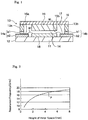
- FIG. 1 An exemplary high frequency package device according to an embodiment of the present invention will be explained referring to Fig. 1 .
- a high frequency package is provided with a bottom plate 11.
- the bottom plate 11 is composed of a metal plate 12.
- a side wall 13 which is formed, for example, in a shape of rectangular frame as a whole is provided on the bottom plate 11 so as to surround a space above the bottom plate 11.
- the side wall 13 has a predetermined height and a width.
- the side wall 13 is composed of metal as a whole.
- a part of side wall, for example, portions 13a, 13b on opposite sides of the rectangular frame are formed with dielectric member 14a, 14b.
- Each of the dielectric member 14a, 14b is composed of upper stage a1, b1 having equal width to metallic side wall 13, and lower stage a2, b2 having larger width than the metallic side wall 13.
- the lower stages a2, b2 of the dielectric member 14a, 14b have inner ends protruded in the internal space 14 and outer ends protruded outside the internal space 14.
- Aband-shaped input line 15a is formed along the full width of the lower stage a2. Therefore, an input line 15a penetrates between the upper stage a1 and the lower stage a2. Also, a band-shaped output line 15b is formed along the full width of lower stage b2. An output line 15b penetrates between the upper stage b1 and the lower stage b2.
- An opening formed by the frame-shaped side wall 13 is sealed with a lid 16, and an air tight internal space 17 is formed on the bottom plate 11 by the side wall 13 and the lid.
- a dielectric plate 18 is arranged on the bottom plate 11 located between two dielectric members 14a, 14b.
- a high frequency circuit (not illustrated) including high frequency transistor, input matching circuit, an output matching circuit and other circuit elements, is formed. Wires W connects between the input line 15a and the high frequency circuit and between the high frequency circuit and the output line 15b.
- a projection 19 protruding toward the bottom plate 11 is formed on a inner surface of the lid 16 at a position between the input line 15a and the output line 15b, for example.
- the projection 19 is made of a same metal material as the lid 16, by joining a metal plate with the lid 16 for example.
- copper, alloy of copper and molybdenum, or a laminated board consisting of these metals are used as a metal material composing the high frequency package device.
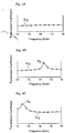
- Fig. 2 is a graph showing an example of a resonant frequency characteristics P of the internal space when a projection is provided on the inner surface of the lid.
- the abscissa indicates height of internal space H (mm) and the ordinate indicates resonant frequency (GHz).
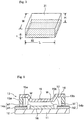
- the internal space 31 has a width W of 16mm and a length equal to a length of the dielectric plate 32 as shown in Fig. 3 .
- the dielectric plate 32 is made of alumina, with the thickness t of 0.25mm.
- the resonant frequency of the internal space becomes low when the height H of the internal space becomes small.
- a ratio of the thickness of the dielectric plate layer to the height H of the internal space becomes greater than the ratio of the thickness of an air layer to the height H of the internal space, and thus, the ratio of the thickness of the dielectric plate layer having a higher specific dielectric constant than that of air layer to the thickness of the air layer becomes large, thereby effectively increasing the relative dielectric constant in the internal space as a whole.
- the resonant frequency of the internal space can be decreased by providing the projection on the inner surface of the lid to reduce the height of the internal space.
- the resonant frequency of the internal space can be set apart greatly from the frequency band used for the high frequency circuit, so that the electric characteristics of the high frequency package device is prevented from deterioration.
- the size of the device is kept small, because the device has such a simple structure that only the projection is formed on the inner surface of the lid. Further, the production of the device is easy because the projection can be formed by simply joining a metal plate to the lid.
- the resonant frequency can be varied greatly with small change in the height of the projection. It is possible in the above embodiment that the projection is not formed over the input line 15a or the output line 15b, so that it is also possible to prevent the wires from contacting with the input line 15a or the output line 15b.
- the abscissas in Figs. 4A to 4C are frequency (GHz), ordinates are transmission coefficient S12.
- transmission coefficient S12 is a ratio of high frequency energy obtained on an output side to the high frequency energy supplied on an input side of the internal space shown in Fig. 3 .
- Fig. 4A shows an example of the resonant characteristics when the internal space width W is 8mm and the height H is 2mm, where resonance of the internal space does not occur in the frequency band (14GHz band) used for the circuit, because the internal space width W is narrow.
- Fig. 4B shows an example of the resonant characteristics when the internal space width W is 16mm and height H is 2mm, where the resonance R2 of the internal space is generated in the frequency band (14GHz band) used for the circuit.
- Fig. 4C shows an example of the resonant characteristics when the internal space width W is 16mm and height H is 0.5mm, which is lower than the height of the internal space shown in Fig. 4B , where the resonance R4 of the internal space shifts to lower frequency (in 12.5GHz frequency band).
- FIG. 5 the same symbols are assigned to the corresponding parts to those in Fig. 1 , and duplicating explanations are omitted.
- a projection 19 at the metal lid 16 is formed by draw processing of the lid 16. Also in this case, height H of the internal space 17, namely the distance between the inner surface of the lid 16 and the bottom plate 11 is decreased, so that a similar function as in the device shown in Fig. 1 is obtained.
- one dielectric plate 18 is arranged on the bottom plate 11 in the internal space 17.
- more than one dielectric plate 18 may be arranged on the bottom plate 11 or other circuit elements may be arranged together with the dielectric plate 18.
Description
- This application is based upon and claims the benefit of priority from the prior Japanese Patent Application No.
2005-201745, filed on July 11, 2005 - The present invention relates to a high frequency package device for storing high frequency circuit used in high frequency bands such as microwave or millimeter wave band.
- High frequency circuits used in high frequency bands are composed of circuit elements, for example, semiconductor elements, capacitors, coils or strip lines, and are stored in an internal space in a high frequency package device.
- The internal space of the high frequency package device corresponds to a sort of cavity in an electromagnetic field. Therefore, it has a resonant frequency dependent on the width of the internal space. A high frequency circuit provided in an internal space is usually used in a frequency band different from the resonant frequency dependent on the internal space width. For example, a resonant frequency dependent on the internal space width is made higher than the frequency used for the high frequency circuit.
- Meanwhile, high frequency circuit stored in high frequency package device has increased in its output power in recent years. With increasing of the output power, number of circuit elements is apt to increase and thus the width of internal space is apt to increase. When the width of the internal space increases, the resonant frequency decreases. As the result, the resonant frequency and the frequency used for the high frequency circuit are getting closer, and thus electric characters of the high frequency circuit degrades.
- In the conventional high frequency package device, a space is divided into two by a separation wall, for example, to make the resonant frequency high when the internal space is very wide, in order to solve the above-mentioned problems (See the Japanese published Patent Application
H5-83010 US6741142 discloses the division of the space into two or more sections by using one or more dividing walls. Alternatively, a height of the internal space is made large with a lid composing the resonant frequency being placed at high position (See the Japanese published Patent Application2000-236045 - However, the method of dividing the internal space with the separation wall sometimes has a drawback that the side wall composing the internal space and the separation wall have different heights resulting in a gap generated at the junction portion between the lid closing an opening of the side wall and the separation wall. Thus, a waveguide mode is generated to degrade electric characteristics of the high frequency package device. On the other hand, the method of increasing the height of internal space has another problem that the height of the package becomes several times as high as an original one if the resonant frequency is required to be changed in sufficient amount, because a degree of the changing the resonant frequency become small as the height of internal space becomes higher. Japanese Patent Application
H5-110310 - A high frequency package device according to one embodiment of the present invention includes all the features of claim 1.
- A more complete appreciation of embodiment of the present invention and many of its attendant advantages will be readily obtained by reference to the following detailed description considered in connection with the accompanying drawings, in which;
-
Fig. 1 is a cross sectional view of an exemplary high frequency package device according to an embodiment of the present invention; -
Fig. 2 is a graph showing an example of resonant frequency characteristics of the internal space in the high frequency package device shown inFig. 1 ; -
Fig. 3 is an exemplary perspective view of the internal space in the high frequency package device shown inFig. 1 for explaining the resonant frequency characteristics; -
Fig. 4A to 4C are graphs showing examples of the resonant frequency characteristics when a width and a height of the internal space shown inFig. 3 is varied; and -
Fig. 5 is a cross sectional view of an example high frequency package device according to another embodiment of the present invention. - An exemplary high frequency package device according to an embodiment of the present invention will be explained referring to
Fig. 1 . - A high frequency package is provided with a
bottom plate 11. Thebottom plate 11 is composed of ametal plate 12. Aside wall 13 which is formed, for example, in a shape of rectangular frame as a whole is provided on thebottom plate 11 so as to surround a space above thebottom plate 11. Theside wall 13 has a predetermined height and a width. Theside wall 13 is composed of metal as a whole. However, a part of side wall, for example,portions dielectric member - Each of the
dielectric member metallic side wall 13, and lower stage a2, b2 having larger width than themetallic side wall 13. The lower stages a2, b2 of thedielectric member internal space 14 and outer ends protruded outside theinternal space 14. Aband-shaped input line 15a is formed along the full width of the lower stage a2. Therefore, aninput line 15a penetrates between the upper stage a1 and the lower stage a2. Also, a band-shaped output line 15b is formed along the full width of lower stage b2. Anoutput line 15b penetrates between the upper stage b1 and the lower stage b2. - An opening formed by the frame-
shaped side wall 13 is sealed with alid 16, and an air tightinternal space 17 is formed on thebottom plate 11 by theside wall 13 and the lid. - A
dielectric plate 18 is arranged on thebottom plate 11 located between twodielectric members dielectric plate 18, a high frequency circuit (not illustrated) including high frequency transistor, input matching circuit, an output matching circuit and other circuit elements, is formed. Wires W connects between theinput line 15a and the high frequency circuit and between the high frequency circuit and theoutput line 15b. - A
projection 19 protruding toward thebottom plate 11 is formed on a inner surface of thelid 16 at a position between theinput line 15a and theoutput line 15b, for example. As the result, a region where a distance between the lower surface of theprojection 19 formed on the inner surface of thelid 16 and thebottom plate 11 is shorter than the distance between the lower surface of thelid 16 where theprojection 19 is not formed and thebottomplate 11. Theprojection 19 is made of a same metal material as thelid 16, by joining a metal plate with thelid 16 for example. Here, copper, alloy of copper and molybdenum, or a laminated board consisting of these metals are used as a metal material composing the high frequency package device. -
Fig. 2 is a graph showing an example of a resonant frequency characteristics P of the internal space when a projection is provided on the inner surface of the lid. InFig. 2 , the abscissa indicates height of internal space H (mm) and the ordinate indicates resonant frequency (GHz). Here, theinternal space 31 has a width W of 16mm and a length equal to a length of thedielectric plate 32 as shown inFig. 3 . Thedielectric plate 32 is made of alumina, with the thickness t of 0.25mm. - As can be seen from the resonant frequency characteristics P in
Fig. 2 , the resonant frequency of the internal space becomes low when the height H of the internal space becomes small. The reason isthat when the height H of the internal space becomes small, a ratio of the thickness of the dielectric plate layer to the height H of the internal space becomes greater than the ratio of the thickness of an air layer to the height H of the internal space, and thus, the ratio of the thickness of the dielectric plate layer having a higher specific dielectric constant than that of air layer to the thickness of the air layer becomes large, thereby effectively increasing the relative dielectric constant in the internal space as a whole. - Thus, the resonant frequency of the internal space can be decreased by providing the projection on the inner surface of the lid to reduce the height of the internal space. As the result, the resonant frequency of the internal space can be set apart greatly from the frequency band used for the high frequency circuit, so that the electric characteristics of the high frequency package device is prevented from deterioration.
- According to the embodiment, the size of the device is kept small, because the device has such a simple structure that only the projection is formed on the inner surface of the lid. Further, the production of the device is easy because the projection can be formed by simply joining a metal plate to the lid.
- Further, variation in the resonant frequency with respect to variation in the height H of the internal space is large in the region where the height H of the internal space is low, as can be seen from the resonant frequency characteristics P in
Fig. 2 . Therefore, the resonant frequency can be varied greatly with small change in the height of the projection. It is possible in the above embodiment that the projection is not formed over theinput line 15a or theoutput line 15b, so that it is also possible to prevent the wires from contacting with theinput line 15a or theoutput line 15b. -
Figs. 4A to 4C are graphs showing examples of transmission coefficient S12 in the internal space shown inFig. 3 , when the thickness t of the dielectric plate is constant (t=0.25mm) and when the width W and the height H of the internal space are varied. The abscissas inFigs. 4A to 4C are frequency (GHz), ordinates are transmission coefficient S12. Here, transmission coefficient S12 is a ratio of high frequency energy obtained on an output side to the high frequency energy supplied on an input side of the internal space shown inFig. 3 . -
Fig. 4A shows an example of the resonant characteristics when the internal space width W is 8mm and the height H is 2mm, where resonance of the internal space does not occur in the frequency band (14GHz band) used for the circuit, because the internal space width W is narrow. -
Fig. 4B shows an example of the resonant characteristics when the internal space width W is 16mm and height H is 2mm, where the resonance R2 of the internal space is generated in the frequency band (14GHz band) used for the circuit. -
Fig. 4C shows an example of the resonant characteristics when the internal space width W is 16mm and height H is 0.5mm, which is lower than the height of the internal space shown inFig. 4B , where the resonance R4 of the internal space shifts to lower frequency (in 12.5GHz frequency band). - As can be seen from the relations in
Figs. 4A to 4C , even if the resonant frequency appears, as shown inFig. 4B , to go down and close to the frequency band used for the high frequency circuit when the internal space width expands, for example, from 8mm to 16mm, those frequencies can be separated from each other, by providing a projection on the inner surface of the lid and lowering the height H of the internal space, so that the electric characteristics of the high frequency package device is prevented from deterioration. - Next, another embodiment of the present invention will be explained referring to the cross sectional view of
Fig. 5 . InFig. 5 , the same symbols are assigned to the corresponding parts to those inFig. 1 , and duplicating explanations are omitted. - In this embodiment, a
projection 19 at themetal lid 16 is formed by draw processing of thelid 16. Also in this case, height H of theinternal space 17, namely the distance between the inner surface of thelid 16 and thebottom plate 11 is decreased, so that a similar function as in the device shown inFig. 1 is obtained. - In the embodiment of
Fig. 1 andFig. 5 , onedielectric plate 18 is arranged on thebottom plate 11 in theinternal space 17. However, more than onedielectric plate 18 may be arranged on thebottom plate 11 or other circuit elements may be arranged together with thedielectric plate 18.
Claims (15)
- A high frequency package device comprising:a bottom plate (11);a side wall (13) provided on the bottom plate (11) and configured to surround a space above the bottom plate (11);
a lid (16) configured to close an opening formed by the side wall (13) and form an internal space (17) on the bottom plate (11) together with the side wall (13);
a dielectric plate (18) arranged on the bottom plate (11) in the internal space (17);
an input line (15a) configured to penetrate the side wall (13);
an output line (15b) configured to penetrate the side wall (13); and
a projection (19) provided on an inner surface of the lid (16) and configured to form a region facing the dielectric plate (18) and to have a surface area, facing the dielectric plate (18), with a lateral length aligned and equal to a lateral length of a surface area of the dielectric plate (18) and not overlapping the input and output lines, where a distance between the lower surface of the projection (19) and the bottom plate (11) is shorter than a distance between the lower surface of the lid (16) where the projection (19) is not provided and the bottom plate (11). - A high frequency package device according to claim 1, wherein the bottom plate (11), the side wall (13), the lid (16), and the projection (19) are composed of metal material.
- A high frequency package device according to claim 2, wherein the projection (19) is located between the input line (15a) and the output line (15b).
- A high frequency package device according to claim 3, wherein the projection (19) is formed by joining a metal plate on a part of the inner surface of the lid (16).
- A high frequency package device according to claim 4, wherein the side wall (13) is formed in a frame shape, and part of the side wall (13) positioned at opposing two sides is formed by dielectric material (14a, 14b), and wherein the input line (15a) and the output line (15b) are so provided as to penetrate the dielectric material (14a, 14b).
- A high frequency package device according to claim 5, wherein the projection (19) is formed at a position opposite to the dielectric plate (18) arranged on the bottom plate (11).
- A high frequency package device according to claim 6, wherein the dielectric plate (18) is a ceramic plate.
- A high frequency package device according to claim 6, wherein the dielectric material (14a, 14b) is composed of an upper stage having the same thickness as the side wall (13) and a lower stage having a larger thickness than the side wall (13), and wherein the input line (15a) or the output line (15b) is laminated on the upper surface of the lower stage.
- A high frequency package device according to claim 8, wherein a high frequency circuit is formed on the dielectric plate (18).
- A high frequency package device according to claim 1, wherein the projection (19) is produced by draw processing of the lid (16) for forming a concave portion.
- A high frequency package device according to claim 10, wherein the side wall (13) is formed in a frame shape, and a part of the side wall (13) positioned at opposing two sides is formed by dielectric material (14a, 14b), and wherein the input line (15a) and the output line (15b) are so provided as to penetrate the dielectric material (14a, 14b).
- A high frequency package device according to claim 11, wherein the projection (19) is formed at a position opposite to the dielectric plate (18) arranged on the bottom plate (11).
- A high frequency package device according to claim 12, wherein the dielectric plate (18) is a ceramic plate.
- A high frequency package device according to claim 12, wherein the dielectric material (14a, 14b) is composed of an upper stage having nearly the same thickness as the side wall (13), and a lower stage having a larger thickness than the side wall (13), and the input line (15a) or the output line (15b) is laminated on the upper surface of the lower stage.
- A high frequency package device according to claim 14, wherein a high frequency circuit is formed on the dielectric plate (18).
Applications Claiming Priority (1)
| Application Number | Priority Date | Filing Date | Title |
|---|---|---|---|
| JP2005201745A JP4575247B2 (en) | 2005-07-11 | 2005-07-11 | High frequency packaging equipment |
Publications (2)
| Publication Number | Publication Date |
|---|---|
| EP1753024A1 EP1753024A1 (en) | 2007-02-14 |
| EP1753024B1 true EP1753024B1 (en) | 2017-09-27 |
Family
ID=37487672
Family Applications (1)
| Application Number | Title | Priority Date | Filing Date |
|---|---|---|---|
| EP06251239.7A Active EP1753024B1 (en) | 2005-07-11 | 2006-03-08 | High frequency package device |
Country Status (6)
| Country | Link |
|---|---|
| US (1) | US7888797B2 (en) |
| EP (1) | EP1753024B1 (en) |
| JP (1) | JP4575247B2 (en) |
| KR (1) | KR100721302B1 (en) |
| CN (1) | CN1897259B (en) |
| TW (1) | TWI320298B (en) |
Families Citing this family (14)
| Publication number | Priority date | Publication date | Assignee | Title |
|---|---|---|---|---|
| JP5377096B2 (en) | 2008-09-08 | 2013-12-25 | 株式会社東芝 | High frequency package device and manufacturing method thereof |
| US9929211B2 (en) * | 2008-09-24 | 2018-03-27 | Qualcomm Incorporated | Reducing spin pumping induced damping of a free layer of a memory device |
| US20100091477A1 (en) * | 2008-10-14 | 2010-04-15 | Kabushiki Kaisha Toshiba | Package, and fabrication method for the package |
| JP5171652B2 (en) * | 2009-01-06 | 2013-03-27 | 三菱電機株式会社 | High frequency module |
| US7990223B1 (en) | 2010-05-31 | 2011-08-02 | Kabushiki Kaisha Toshiba | High frequency module and operating method of the same |
| CN104041195B (en) | 2012-10-17 | 2016-12-21 | 华为技术有限公司 | Opto-electronic device |
| KR20150075347A (en) | 2013-12-25 | 2015-07-03 | 가부시끼가이샤 도시바 | Semiconductor package, semiconductor module and semiconductor device |
| JP5921586B2 (en) * | 2014-02-07 | 2016-05-24 | 株式会社東芝 | Millimeter-wave band semiconductor package and millimeter-wave band semiconductor device |
| JP2015149650A (en) | 2014-02-07 | 2015-08-20 | 株式会社東芝 | Millimeter waveband semiconductor package and millimeter waveband semiconductor device |
| JP2015149649A (en) * | 2014-02-07 | 2015-08-20 | 株式会社東芝 | Millimeter waveband semiconductor package and millimeter waveband semiconductor device |
| JP6455402B2 (en) | 2015-11-16 | 2019-01-23 | 三菱電機株式会社 | Microwave and millimeter wave packages |
| FR3066643B1 (en) * | 2017-05-16 | 2020-03-13 | Stmicroelectronics (Grenoble 2) Sas | ELECTRONIC BOX PROVIDED WITH A LOCAL VENT-FORMING SLOT |
| CN109887904A (en) * | 2019-04-16 | 2019-06-14 | 中国电子科技集团公司第十三研究所 | A kind of encapsulating structure and printed circuit board of millimeter wave chip |
| CN110444511A (en) * | 2019-07-23 | 2019-11-12 | 中国科学技术大学 | Improve the Package boxes structure of Superconducting Quantum Processor resonance frequency |
Citations (1)
| Publication number | Priority date | Publication date | Assignee | Title |
|---|---|---|---|---|
| JPH05110310A (en) * | 1991-10-16 | 1993-04-30 | Fujitsu Ltd | Microwave circuit |
Family Cites Families (42)
| Publication number | Priority date | Publication date | Assignee | Title |
|---|---|---|---|---|
| US4975762A (en) * | 1981-06-11 | 1990-12-04 | General Electric Ceramics, Inc. | Alpha-particle-emitting ceramic composite cover |
| JPS596303U (en) * | 1982-07-05 | 1984-01-17 | 株式会社東芝 | High frequency circuit equipment |
| JPH01107141A (en) | 1987-10-20 | 1989-04-25 | Daido Steel Co Ltd | Non-destructive determining method of weld penetration |
| JPH01107141U (en) * | 1988-01-07 | 1989-07-19 | ||
| JPH01314401A (en) | 1988-06-15 | 1989-12-19 | Fujitsu Ltd | Micro-wave and millimeter wave module |
| US5268533A (en) * | 1991-05-03 | 1993-12-07 | Hughes Aircraft Company | Pre-stressed laminated lid for electronic circuit package |
| JPH0583010A (en) | 1991-09-19 | 1993-04-02 | Nec Corp | Semiconductor device |
| JPH05121888A (en) | 1991-10-28 | 1993-05-18 | Fujitsu Ltd | High-frequency circuit device |
| TW238419B (en) * | 1992-08-21 | 1995-01-11 | Olin Corp | |
| US6611054B1 (en) * | 1993-12-22 | 2003-08-26 | Honeywell Inc. | IC package lid for dose enhancement protection |
| JP2734364B2 (en) * | 1993-12-30 | 1998-03-30 | 日本電気株式会社 | Semiconductor device |
| JP3378435B2 (en) * | 1995-09-29 | 2003-02-17 | 株式会社東芝 | Ultra-high frequency band wireless communication device |
| JP3500268B2 (en) * | 1997-02-27 | 2004-02-23 | 京セラ株式会社 | High frequency input / output terminal and high frequency semiconductor element storage package using the same |
| JP3013812B2 (en) * | 1997-07-15 | 2000-02-28 | 住友電気工業株式会社 | Semiconductor container and semiconductor module |
| US6057600A (en) | 1997-11-27 | 2000-05-02 | Kyocera Corporation | Structure for mounting a high-frequency package |
| JPH11238823A (en) | 1998-02-23 | 1999-08-31 | Toshiba Corp | Semiconductor package |
| US6483406B1 (en) | 1998-07-31 | 2002-11-19 | Kyocera Corporation | High-frequency module using slot coupling |
| JP2000236045A (en) * | 1999-02-16 | 2000-08-29 | Mitsubishi Electric Corp | High-frequency package |
| JP3929197B2 (en) * | 1999-03-17 | 2007-06-13 | 松下電器産業株式会社 | High frequency circuit element |
| JP3739230B2 (en) * | 1999-04-26 | 2006-01-25 | 株式会社日立製作所 | High frequency communication equipment |
| US6392298B1 (en) * | 2000-02-28 | 2002-05-21 | Ericsson Inc. | Functional lid for RF power package |
| JP2001274278A (en) * | 2000-03-27 | 2001-10-05 | Toshiba Corp | Microwave semiconductor device and its manufacturing method |
| JP2002343982A (en) * | 2001-05-16 | 2002-11-29 | Mitsubishi Electric Corp | Optical module, optical transmitter, and optical receiver |
| US6472962B1 (en) * | 2001-05-17 | 2002-10-29 | Institute Of Microelectronics | Inductor-capacitor resonant RF switch |
| JP2003008309A (en) * | 2001-06-25 | 2003-01-10 | Nec Corp | Microwave-band interference preventing package |
| US6586863B2 (en) * | 2001-06-28 | 2003-07-01 | Samsung Electro-Mechanics Co., Ltd. | Rosen type piezoelectric transformer with multiple output electrodes |
| JP4610134B2 (en) * | 2001-08-09 | 2011-01-12 | 京セラ株式会社 | High frequency circuit package |
| US6531668B1 (en) * | 2001-08-30 | 2003-03-11 | Intel Corporation | High-speed MEMS switch with high-resonance-frequency beam |
| JP3973402B2 (en) * | 2001-10-25 | 2007-09-12 | 株式会社日立製作所 | High frequency circuit module |
| JP3735569B2 (en) * | 2001-12-26 | 2006-01-18 | 京セラ株式会社 | High frequency circuit package lid and high frequency circuit package using the same |
| JP3922039B2 (en) * | 2002-02-15 | 2007-05-30 | 株式会社日立製作所 | Electromagnetic wave absorbing material and various products using the same |
| US6853072B2 (en) * | 2002-04-17 | 2005-02-08 | Sanyo Electric Co., Ltd. | Semiconductor switching circuit device and manufacturing method thereof |
| US6822541B2 (en) * | 2002-04-25 | 2004-11-23 | Kyocera Corporation | Electromagnetic wave absorber and high-frequency circuit package using the same |
| JP3830430B2 (en) * | 2002-07-09 | 2006-10-04 | 京セラ株式会社 | High frequency circuit package lid, manufacturing method thereof, and high frequency circuit package using the same |
| JP2004111570A (en) * | 2002-09-17 | 2004-04-08 | Kyocera Corp | Package for high frequency circuit |
| JP2004214577A (en) * | 2003-01-09 | 2004-07-29 | Mitsubishi Electric Corp | Packaging case for microwave integrated circuit |
| US7378655B2 (en) * | 2003-04-11 | 2008-05-27 | California Institute Of Technology | Apparatus and method for sensing electromagnetic radiation using a tunable device |
| JP2005050861A (en) * | 2003-07-29 | 2005-02-24 | Kyocera Corp | Package lid for semiconductor element, and semiconductor element package using this |
| JP3829839B2 (en) * | 2003-11-14 | 2006-10-04 | 三菱電機株式会社 | High frequency package |
| GB0328246D0 (en) * | 2003-12-04 | 2004-06-16 | Qinetiq Ltd | Improvements relating to electronic circuit packages |
| US7405924B2 (en) * | 2004-09-27 | 2008-07-29 | Idc, Llc | System and method for protecting microelectromechanical systems array using structurally reinforced back-plate |
| JP4519637B2 (en) * | 2004-12-28 | 2010-08-04 | 株式会社東芝 | Semiconductor device |
-
2005
- 2005-07-11 JP JP2005201745A patent/JP4575247B2/en active Active
-
2006
- 2006-03-06 US US11/367,460 patent/US7888797B2/en active Active
- 2006-03-08 KR KR1020060021767A patent/KR100721302B1/en active IP Right Grant
- 2006-03-08 EP EP06251239.7A patent/EP1753024B1/en active Active
- 2006-03-09 TW TW095107954A patent/TWI320298B/en active
- 2006-03-10 CN CN200610058503XA patent/CN1897259B/en active Active
Patent Citations (1)
| Publication number | Priority date | Publication date | Assignee | Title |
|---|---|---|---|---|
| JPH05110310A (en) * | 1991-10-16 | 1993-04-30 | Fujitsu Ltd | Microwave circuit |
Also Published As
| Publication number | Publication date |
|---|---|
| CN1897259B (en) | 2011-01-26 |
| CN1897259A (en) | 2007-01-17 |
| JP2007019403A (en) | 2007-01-25 |
| JP4575247B2 (en) | 2010-11-04 |
| KR20070007705A (en) | 2007-01-16 |
| TWI320298B (en) | 2010-02-01 |
| TW200704334A (en) | 2007-01-16 |
| US20070007647A1 (en) | 2007-01-11 |
| EP1753024A1 (en) | 2007-02-14 |
| US7888797B2 (en) | 2011-02-15 |
| KR100721302B1 (en) | 2007-05-28 |
Similar Documents
| Publication | Publication Date | Title |
|---|---|---|
| EP1753024B1 (en) | High frequency package device | |
| US11670829B2 (en) | Radar assembly with rectangular waveguide to substrate integrated waveguide transition | |
| US7323954B2 (en) | Dielectric ceramic filter with metal guide-can | |
| US4713634A (en) | Semiconductor device mounted in a housing having an increased cutoff frequency | |
| JP3829839B2 (en) | High frequency package | |
| JP2004235184A (en) | High frequency device | |
| JPH09321501A (en) | Multilayer high frequency circuit board | |
| JP3204241B2 (en) | Waveguide connection package | |
| WO2007108262A1 (en) | Transmitter/receiver | |
| EP0841714B1 (en) | Dielectric resonator apparatus and high-frequency module | |
| JP6703342B2 (en) | High frequency equipment | |
| JP2001028504A (en) | Circulator | |
| EP1455410B1 (en) | Bandpass filter | |
| JP3383203B2 (en) | Package for microwave circuit | |
| US10340224B2 (en) | Microwave and millimeter wave package | |
| JP3441975B2 (en) | High frequency package | |
| JP2001345606A (en) | Mmic amplifier | |
| JPH10107519A (en) | High frequency module | |
| JPH05110310A (en) | Microwave circuit | |
| JP4095263B2 (en) | High frequency package | |
| JPH10270586A (en) | Antenna integrated high frequency semiconductor module | |
| GB2601333A (en) | Electromagnetic interference shield device | |
| JP4401886B2 (en) | High frequency package | |
| JPH04294568A (en) | Semiconductor device for microwave use | |
| JPH09148470A (en) | Semiconductor enclosure for high frequency |
Legal Events
| Date | Code | Title | Description |
|---|---|---|---|
| PUAI | Public reference made under article 153(3) epc to a published international application that has entered the european phase |
Free format text: ORIGINAL CODE: 0009012 |
|
| 17P | Request for examination filed |
Effective date: 20060315 |
|
| AK | Designated contracting states |
Kind code of ref document: A1 Designated state(s): AT BE BG CH CY CZ DE DK EE ES FI FR GB GR HU IE IS IT LI LT LU LV MC NL PL PT RO SE SI SK TR |
|
| AX | Request for extension of the european patent |
Extension state: AL BA HR MK YU |
|
| AKX | Designation fees paid |
Designated state(s): DE FR GB |
|
| 17Q | First examination report despatched |
Effective date: 20071011 |
|
| REG | Reference to a national code |
Ref country code: DE Ref legal event code: R079 Ref document number: 602006053705 Country of ref document: DE Free format text: PREVIOUS MAIN CLASS: H01L0023020000 Ipc: H01L0023047000 |
|
| GRAP | Despatch of communication of intention to grant a patent |
Free format text: ORIGINAL CODE: EPIDOSNIGR1 |
|
| STAA | Information on the status of an ep patent application or granted ep patent |
Free format text: STATUS: GRANT OF PATENT IS INTENDED |
|
| RIC1 | Information provided on ipc code assigned before grant |
Ipc: H01L 23/047 20060101AFI20170404BHEP Ipc: H01L 23/00 20060101ALI20170404BHEP Ipc: H01L 23/66 20060101ALI20170404BHEP |
|
| INTG | Intention to grant announced |
Effective date: 20170425 |
|
| RIN1 | Information on inventor provided before grant (corrected) |
Inventor name: TAKAGI, KAZUTAKA |
|
| GRAS | Grant fee paid |
Free format text: ORIGINAL CODE: EPIDOSNIGR3 |
|
| GRAA | (expected) grant |
Free format text: ORIGINAL CODE: 0009210 |
|
| STAA | Information on the status of an ep patent application or granted ep patent |
Free format text: STATUS: THE PATENT HAS BEEN GRANTED |
|
| AK | Designated contracting states |
Kind code of ref document: B1 Designated state(s): DE FR GB |
|
| REG | Reference to a national code |
Ref country code: GB Ref legal event code: FG4D |
|
| REG | Reference to a national code |
Ref country code: DE Ref legal event code: R096 Ref document number: 602006053705 Country of ref document: DE |
|
| REG | Reference to a national code |
Ref country code: FR Ref legal event code: PLFP Year of fee payment: 13 |
|
| REG | Reference to a national code |
Ref country code: DE Ref legal event code: R097 Ref document number: 602006053705 Country of ref document: DE |
|
| PLBE | No opposition filed within time limit |
Free format text: ORIGINAL CODE: 0009261 |
|
| STAA | Information on the status of an ep patent application or granted ep patent |
Free format text: STATUS: NO OPPOSITION FILED WITHIN TIME LIMIT |
|
| 26N | No opposition filed |
Effective date: 20180628 |
|
| PGFP | Annual fee paid to national office [announced via postgrant information from national office to epo] |
Ref country code: GB Payment date: 20230112 Year of fee payment: 18 Ref country code: DE Payment date: 20230110 Year of fee payment: 18 |
|
| PGFP | Annual fee paid to national office [announced via postgrant information from national office to epo] |
Ref country code: FR Payment date: 20231229 Year of fee payment: 19 |