JP3929197B2 - High frequency circuit element - Google Patents
High frequency circuit element Download PDFInfo
- Publication number
- JP3929197B2 JP3929197B2 JP07164499A JP7164499A JP3929197B2 JP 3929197 B2 JP3929197 B2 JP 3929197B2 JP 07164499 A JP07164499 A JP 07164499A JP 7164499 A JP7164499 A JP 7164499A JP 3929197 B2 JP3929197 B2 JP 3929197B2
- Authority
- JP
- Japan
- Prior art keywords
- frequency circuit
- input
- order mode
- circuit element
- frequency
- Prior art date
- Legal status (The legal status is an assumption and is not a legal conclusion. Google has not performed a legal analysis and makes no representation as to the accuracy of the status listed.)
- Expired - Fee Related
Links
Images


Classifications
-
- H—ELECTRICITY
- H01—ELECTRIC ELEMENTS
- H01L—SEMICONDUCTOR DEVICES NOT COVERED BY CLASS H10
- H01L23/00—Details of semiconductor or other solid state devices
- H01L23/552—Protection against radiation, e.g. light or electromagnetic waves
-
- H—ELECTRICITY
- H01—ELECTRIC ELEMENTS
- H01P—WAVEGUIDES; RESONATORS, LINES, OR OTHER DEVICES OF THE WAVEGUIDE TYPE
- H01P1/00—Auxiliary devices
- H01P1/16—Auxiliary devices for mode selection, e.g. mode suppression or mode promotion; for mode conversion
-
- H—ELECTRICITY
- H01—ELECTRIC ELEMENTS
- H01L—SEMICONDUCTOR DEVICES NOT COVERED BY CLASS H10
- H01L2924/00—Indexing scheme for arrangements or methods for connecting or disconnecting semiconductor or solid-state bodies as covered by H01L24/00
- H01L2924/15—Details of package parts other than the semiconductor or other solid state devices to be connected
- H01L2924/161—Cap
- H01L2924/1615—Shape
- H01L2924/16152—Cap comprising a cavity for hosting the device, e.g. U-shaped cap
- H01L2924/1616—Cavity shape
-
- H—ELECTRICITY
- H01—ELECTRIC ELEMENTS
- H01L—SEMICONDUCTOR DEVICES NOT COVERED BY CLASS H10
- H01L2924/00—Indexing scheme for arrangements or methods for connecting or disconnecting semiconductor or solid-state bodies as covered by H01L24/00
- H01L2924/15—Details of package parts other than the semiconductor or other solid state devices to be connected
- H01L2924/161—Cap
- H01L2924/1615—Shape
- H01L2924/16195—Flat cap [not enclosing an internal cavity]
Description
【0001】
【発明の属する技術分野】
本発明は、通信システムなどの高周波信号処理装置に用いられるフィルタなどの高周波回路素子に関する。
【0002】
【従来の技術】
高周波通信システムにおいては、フィルタや分波器などの高周波回路素子は不可欠の要素であるが、従来から用いられている共振器フィルタなどの高周波回路素子では、電磁界エネルギーの放射や外界からの電磁気的ノイズの混入を防ぐために、共振器部分を金属筐体に納め、電磁気的にシールドする構造をとる場合が多い。
【0003】
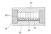
図7および図8に、伝送線路構造を用いた従来の高周波回路素子の概略構成の一例を示す。なお、図7では、この高周波回路素子の筐体内部の構造が見えるように、図8に示した筐体蓋部81の図示を省略した。
【0004】
図7および図8に示すように、上記従来の高周波回路素子は、誘電体単結晶などからなる基板85の上面に、ストリップ導体パターンによるλ/2共振器86a〜86dと、入出力線路87a・87bとが形成されている。λ/2共振器86a〜86dと、入出力線路87a・87bと、グランドプレーン88とによって、マイクロストリップ構造の高周波回路が構成されている。この高周波回路は、4つのλ/2共振器86a〜86dが結合した構造になっており、4段の帯域通過フィルタとして機能する。
【0005】
この高周波回路素子の筐体は、導体材料によって形成され、図8に示す筐体蓋部81、筐体枠部82、および筐体底部83からなる。この筐体とグランドプレーン88とが電気的に接続されるよう、基板85が筐体底部83に、例えば導電性の接着剤により接着されている。
【0006】
筐体枠部82の側面には、同軸コネクターによる入出力端子84a・84bが配設されいる。入出力端子84a・84bの内導体は入出力線路87a・87bに、入出力端子84a・84bの外導体は筐体に、それぞれ電気的に接続されている。
【0007】
図9および図10に、ストリップ導体パターンを使用した従来の高周波素子の他の例を示す。なお、図9においても、この高周波回路素子の筐体内部の構造が見えるように、図10に示した筐体蓋部81の図示を省略した。図9および図10に示す構成では、8つのヘアピン型共振器89a〜89hを共振器として使用し、8段の帯域通過フィルタを構成している。その他の部分の構造は、図7および図8に示した従来の高周波回路素子と同様である。
【0008】
以上のように構成された従来の高周波回路素子において、例えば入出力端子84aより高周波信号が入力されると、マイクロストリップ導体伝送線路である入出力線路87aを、図11に示すように、基本モードである準TEMモードの電磁波が伝播する。なお、図11は、入出力線路87aに垂直な面に沿って筐体を切断したときの切断面を示すものであり、3次元電磁界シミュレーション(ヒューレット・パッカード社製のHFSS)による解析結果を基に、電界の向きを模式的に表した図である。
【0009】
入出力線路87aを伝播した準TEMモードの電磁波が、各共振器86a〜86dあるいは89a〜89hにおいて共振現象を起こすことにより、帯域通過フィルタとして動作する。したがって、フィルタの帯域内信号のみが、入出力線路87a・87bを通過して出力される。
【0010】
【発明が解決しようとする課題】
しかしながら、上記した従来の高周波回路素子では、電磁波がストリップ導体伝送線路を伝播する準TEMモードだけでなく、入出力端子84a・84bから入出力線路87a・87bへの変換部分の不連続性や、準TEMモードの放射電界成分が原因となって、図12に示すように、筐体蓋部81と基板85との間の空間部を電磁波が伝播する不要な高次モードである導波管モードも励振され、高周波回路素子の周波数特性に悪影響を及ぼすという問題がある。なお、図12は、図11と同様に入出力線路87aに垂直な面に沿って筐体を切断したときの切断面を示すものであり、3次元電磁界シミュレーションによる解析結果を示す。
【0011】
こうした導波管モードは、準TEMモードと異なり、フィルタの作用とは無関係なため、フィルタの通過帯域とは関係なく電磁波を伝播し、高周波回路素子のフィルタとしての特性を悪化させる。特に、阻止帯域の減衰量の低下、すなわちバックグラウンドレベルの上昇が問題であり、フィルタの帯域外信号阻止能力の低下が起こる。
【0012】
こうした導波管モード(不要高次モード)の影響を低減させるためには、筐体蓋部81と基板85との間の空間部の遮断周波数がフィルタの中心周波数より十分高い周波数になるよう筐体の設計を行うことも考えられるが、阻止帯域では例えば−80dB以下という大きな減衰量が必要とされるため、わずかな高周波信号の伝播も問題であり、遮断周波数を考慮した筐体の設計のみによる対策では不十分である。
【0013】
また、この問題は、高周波回路素子を小型化したり、動作周波数を高くしたり、あるいは、低損失化を図るために超伝導体のような導電率の大きな材料を用いたりすることが必要な場合に、さらに顕著化する。
【0014】
本発明は、前記した問題を解決するために、高周波回路素子の金属筐体の内部空間において不要高次モードの発生を防止することにより、周波数特性の優れた高性能な高周波回路素子を提供することを目的とする。
【0015】
【課題を解決するための手段】
前記目的を達成するため、本発明に係る高周波回路素子の第1の構成は、基板と、前記基板に形成された高周波回路と、前記基板を内包することにより前記高周波回路を電磁界的にシールドする金属筐体と、前記金属筐体に配設され前記高周波回路に高周波信号を入出力し、前記高周波回路に対応する入出力線路と接続されている入出力端子と、前記入出力線路の少なくとも一つに対して電気的に接触することなく略垂直に跨いで配置され、前記入出力線路と前記入出力端子の接続部を前記高周波回路から隔離することにより、前記金属筐体の内部空間における高周波の伝搬経路を遮断する不要高次モード遮断板とを有し、前記不要高次モード遮断板が、前記金属筐体の内部空間を分断し、前記不要高次モード遮断板が高誘電率誘電体により構成されていることを特徴とする。
【0016】
前記の高周波回路素子の第1の構成によれば、不要高次モード遮断板を有することにより、筐体内部の空間部分で発生する導波管モードの電磁波の伝播が抑制されるので、不要な高次モードの励起による周波数特性の悪化を防ぐことができる。従って、周波数特性の優れた高性能な高周波回路素子を提供することが可能となる。
【0022】
この構成によれば、誘電体により反射あるいは吸収されることによって、電磁波が不要高次モード遮断板を透過できないことから、不要な高次モードの伝播を抑制する効果を高めることができる。
【0025】
また、前記の高周波回路素子の第1の構成において、不要高次モード遮断板が、前記高周波回路の入出力線路に電気的に接触しないよう切り欠きを有することが望ましい。
【0026】
この構成によれば、不要高次モード遮断板の下端部を、高周波回路が存在しない部分においては、基板に接触する位置まで延長できるので、不要高次モードを抑制する能力をよりいっそう高めることができる。
【0035】
また、前記の高周波回路素子の第1の構成において、高周波回路が高周波フィルタであることが望ましい。
【0036】
この構成によれば、不要高次モード遮断板に不要な高次モードの励起が抑制されるため、帯域外の周波数においてフィルタの作用にかからない高次モードが伝播し出力されてしまうことを防ぐことができるので、帯域外の減衰特性の優れたフィルタを実現することができる。
【0037】
さらに、前記の高周波回路素子の第1の構成において、高周波回路の高周波フィルタが、互いに結合された複数の平面回路共振器を有することが望ましい。
【0038】
この構成によれば、共振器よりの放射で励起される不要高次モードが入出力線路入射されて入出力端子より出力されるのを防ぐことができるため、帯域外の周波数においてフィルタの作用にかからない高次モードが伝播し出力されてしまうことを防ぐことができる。これにより、帯域外の減衰特性の優れたフィルタを実現することができる。
【0039】
また、前記の高周波回路素子の第1の構成において、高周波回路が超伝導高周波フィルタであることが望ましい。
【0040】
この構成によれば、共振器での導体損失を劇的に低減することが可能となり、低損失、かつ、急峻なスカート特性を実現できる。
【0041】
【発明の実施の形態】
以下、本発明の実施の形態について、図面を参照しながら説明する。
【0042】
(実施の形態1)
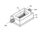
図1および図2に、本発明の実施の一形態にかかる高周波回路素子の概略構成を示す。なお、図1において、筐体の内部構造が見えるように、図2に示した筐体蓋部11の図示を省略した。
【0043】
図1および図2に示すように、本実施形態の高周波回路素子は、誘電体単結晶などからなる基板15の上面に、ストリップ導体パターンによるヘアピン型共振器16a〜16hおよび入出力線路17a・17bが形成されている。これらのヘアピン型共振器16a〜16hと、入出力線路17a・17bと、グランドプレーン18により、マイクロストリップ構造の高周波回路が構成されている。この高周波回路は、8つのヘアピン型共振器16a〜16hが結合した構造になっており、8段の帯域通過フィルタとして機能する。
【0044】
また、本高周波回路素子は、上記の高周波回路を内包して電磁気的にシールドする筐体を備えている。この筐体は、導体材料により形成され、図2に示すように、筐体蓋部11、筐体枠部12、および筐体底部13から構成される。この筐体とグランドプレーン18とが電気的に接続されるように、基板15が筐体底部13に、例えば導電性の接着剤により固定されている。
【0045】
また、筐体枠部12の側面には、同軸コネクターによる入出力端子14a・14bが配設されている。入出力端子14a・14bの内導体は、入出力線路17a・17bに、入出力端子14a・14bの外導体は、筐体枠部12に電気的に接続されている。
【0046】
また、本高周波回路素子は、導体材料からなる不要高次モード遮断板1a〜1cを備えている。不要高次モード遮断板1a〜1cは、筐体に電気的に接続されるよう例えば導電性の接着剤により筐体枠部12に固定され、筐体の内部空間を略分断することによって、高周波の伝播経路を遮断する。
【0047】
上記の不要高次モード遮断板1a〜1cのうち、中央に位置する不要高次モード遮断板1bは、ヘアピン型共振器16aと16hとの間に配置される。このため、不要高次モード遮断板1bは、高周波回路のストリップ導体(ヘアピン型共振器16a〜16h)に接触しないように、基板15との間に一定の間隙を保って、筐体枠部12に固定される。
【0048】
一方、両端に位置する不要高次モード遮断板1a・1cは、ヘアピン型共振器16aおよび16hのそれぞれよりも外側、すなわち入出力線路17a・17bを跨ぐように配置される。このため、不要高次モード遮断板1a・1cは、入出力線路17a・17bに接触しないように半円形の切り欠き部を持つ。不要高次モード遮断板1a・1cにおける切り欠き部以外の下端部は、基板15との間に間隙が生じないように、基板15の表面に密着して配設されている。
【0049】
なお、不要高次モード遮断板1a・1cは、入出力線路17a・17bに対して略垂直に設けることが好ましい。これにより、入出力端子14a・14bと入出力線路17a・17bとの接続部が、高周波回路の主要回路であるヘアピン型共振器16aおよび16hと隔離されるので、接続部の不連続性が原因で励起される不要高次モードの電磁波が高周波回路に悪影響を与えるのを防止できる。
【0050】
また、前述したように、導体材料からなる不要高次モード遮断板1a〜1cを、筐体枠部12に電気的に接続した構成とすることにより、不要高次モード遮断板1a〜1cが電磁波に対して電気壁として作用するため、不要な高次モードの伝播を抑制する効果が向上する。
【0051】
また、本発明では、不要高次モード遮断板1a〜1cを高誘電率誘電体により形成する。この構成によれば、電磁波が誘電体により反射あるいは吸収されて不要高次モード遮断板1a〜1cを透過できないことから、不要な高次モードの伝播を抑制する効果を高めることができる。なお、誘電率が高くなるほど反射係数が大きくなるので効果が増大し、比誘電率が約10以上の高誘電率誘電体を用いれば、誘電体境界上での反射係数が約0.5以上となり、顕著な効果が得られるので特に好ましい。
【0052】
次に、以上のように構成された本実施形態の高周波回路素子の動作について説明する。
【0053】
入出力端子14aを入力側、入出力端子14bを出力側としたとすると、入出力端子14aから入力された高周波信号は、同軸線路の基本モードであるTEMモードから、マイクロストリップ線路の基本モードである準TEMモード(図11参照)に変換され、入出力線路17aに沿って伝播し、高周波回路に入力される。
【0054】
高周波回路は、ヘアピン型共振器16a〜16hの各々が共振現象を起こすことにより、帯域通過フィルタとして動作する。従って、入出力線路17bに、帯域フィルタの通過帯域に相当する周波数帯域の信号のみが、準TEMモードで出力され、再びTEMモードに変換されて入出力端子14bから出力される。
【0055】
なお、筐体蓋部11、筐体枠部12、および筐体底部13から構成される筐体は、入出力線路17a・17bおよび高周波回路を構成するマイクロストリップ導体(ヘアピン型共振器16a〜16h)からの高周波信号の放射による電磁界エネルギーの損失や外界からの電磁気的ノイズの混入を防ぐ役割を持つ。
【0056】
本高周波回路素子は、以上のように、マイクロストリップ導体の基本モードで動作するが、入出力端子14aから入出力線路17aへの伝播モード変換や、マイクロストリップ導体からの電磁波の放射により、基本モード以外の不要な高次モードである、筐体を矩形導波管とした導波管モード(図12参照)が発生することを防止する必要がある。
【0057】
そこで、本実施形態の高周波回路素子では、不要高次モード遮断板1a〜1cが、基板15と筐体との間の空間を伝播する電磁波に対して電気壁として作用することにより、このような不要な高次モードの電磁波が伝播することを防ぐことができる。
【0058】
ここで、不要高次モード遮断板1a〜1cの効果を確かめるための比較実験の結果について、図3および図4を用いて説明する。
【0059】
まず、比較実験を行うために、本実施形態の高周波回路素子を、以下のような条件で作成した。
【0060】
基板15として、短辺の長さが12.7mm、長辺の長さが25.4mm、厚さが0.5mm、誘電率が24の高誘電率誘電体であるLaAl2O3を用い、その一方の表面に超伝導体であるYBCOを蒸着することによりグランドプレーン18を形成した。また、基板15の他の表面に、同じく超伝導体であるYBCOにより0.5mm幅の入出力線路17a・17bおよび中心周波数1.9GHzの帯域通過フィルタとして設計されたヘアピン型共振器16a〜16hを蒸着およびエッチング等により形成した。
【0061】
また、黄銅を機械加工し、表面を金メッキ処理することにより、筐体を作成した。なお、筐体の外形寸法を37.8mm×25.1mm×15mmとし、内側寸法を25.6mm×12.9mm×4.1mmとした。
【0062】
さらに、黄銅を機械加工し、表面を金メッキ処理することにより、不要高次モード遮断板1a・1cを作成した。不要高次モード遮断板1a・1cの各々は、長辺の長さを12.9mm、短辺の長さを3.6mm、厚さを0.3mmとし、切り欠き部の半径を2mmとした。
【0063】
また、黄銅を機械加工し、表面を金メッキ処理することにより、長辺の長さが12.9mm、短辺の長さが3.3mm、厚さが0.3mmの不要高次モード遮断板1bを作成した。
【0064】
不要高次モード遮断板1a・1cの各々を、筐体の入出力端子14a・14bが各々設けられた面の内側面より3mm離れた位置に設置し、不要高次モード遮断板1bを、不要高次モード遮断板1a・1cの中央に設置した。
【0065】
以上の条件で作成した本実施形態の高周波回路素子の周波数特性を測定すると、図3に示すとおりとなった。なお、測定は、絶対温度64Kの冷却環境下で行った。
【0066】
そして、比較例として、不要高次モード遮断板1a〜1cを設けない以外は、上記した条件と同一条件によって高周波回路素子を作成し、絶対温度64Kの冷却環境下において、周波数特性を測定すると、図4に示すとおりの結果が得られた。
【0067】
図3と図4とを比較することから明らかなように、本実施形態の高周波回路素子は、不要高次モード遮断板1a〜1cの効果により、阻止帯域の減衰量が、従来の約−70dBから約−80dBへと、−10dB程度改善されており、フィルタとして、帯域外の不要な周波数帯域の信号を除去する能力が向上したことが分かる。
【0068】
以上のように、本実施形態にかかる高周波回路素子は、不要高次モード遮断板1a〜1cを備えたことにより、周波数特性の改善が達成されている。
【0069】
なお、上記の説明では、不要高次モード遮断板1a〜1cを別個に形成し、導電性接着剤等によって筐体枠部12と接着固定するものとしたが、導電性接着剤の代わりに導電性のネジを用いてもよい。また、固定先は筐体枠部12に限らず、例えば、不要高次モード遮断板1a〜1cを筐体蓋部11に導電性接着剤またはネジにより固定し、筐体枠部12に金属接触させて導通をとる構造とすることも可能である。あるいは、不要高次モード遮断板1a〜1cを筐体と一体形成することも可能である。
【0070】
また、不要高次モード遮断板の枚数およびその設置位置、さらに、切り欠き部の形状や寸法、板厚、材料の導電率等の最適値は、高周波回路の構造や筐体の構造により異なるので、上記した具体例にのみ限定されるものではない。つまり、上記の説明では、直方体形状の筐体内部空間を不要高次モード遮断板により3つに略分断した構成を例示したが、これに限らず、入出力端子14aおよび入出力線路17aの接続部分(不連続部)と、入出力端子14bおよび入出力線路17bの接続部分(不連続部)とが、互いに異なる空間に属するように分断あるいは隔離される構成であれば、周波数特性の改善効果が得られる。
【0071】
従って、不要高次モード遮断板の枚数は、3枚に限られるわけでない。また、不要高次モード遮断板の形状も、上述した形状に限定されるものではなく、切り欠き部の形状も半円形に限定されず、例えば三角形状等であっても効果を発揮し得ることは言うまでもない。
【0072】
また、不要高次モード遮断板の材質に関しても、導体に限られるわけではなく、電磁波を透過させない性質の材料であればよい。従って、電磁波を反射あるいは吸収する性質を持つ、高誘電率誘電体を用いてもよい。例えば、誘電率が24のLaAl2O3の板材を基板と同様に切り出したものを使用しても、同様の効果を発揮する。
【0073】
(参考形態1)
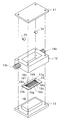
図5および図6に、参考形態1にかかる高周波回路素子の概略構成を示す。なお、図5においては、筐体の内部構造が見えるように、図6に示した筐体蓋部11の図示を省略した。
【0074】
本参考形態の高周波回路素子は、実施の形態1にかかる高周波回路素子が備える不要高次モード遮断板1a〜1cの代わりに、図6に示すように、導体材料により形成された不要高次モード遮断カバー2a・2bを備えている。その他の部分の構造は、図1および図2に示した実施の形態1にかかる高周波回路素子と同様であるので、説明は省略する。
【0075】
不要高次モード遮断カバー2a・2bは、半円筒形状で、基板15上の入出力線路17a・17bをそれぞれ覆うように配設され、筐体に電気的に接続されるよう、例えば導電性の接着剤により、筐体枠部12における入出力端子14a・14bが接続されている面の内側面にそれぞれ固定されている。
【0076】
本参考形態の高周波回路素子も、高周波回路を構成するヘアピン型共振器16a〜16hの作用により、帯域通過フィルタとして動作する点においては、実施の形態1の高周波回路素子と同様である。また、本参考形態の高周波回路素子においても、入出力端子14aから入出力線路17aへの伝播モード変換の際に励起される電磁波や、マイクロストリップ導体すなわちヘアピン型共振器16a〜16hからの電磁波の放射により、基本モード以外の不要な高次モードである、筐体を矩形導波管とした導波管モード(図12参照)の発生を防止することが必要である。
【0077】
本参考形態の高周波回路素子では、入出力端子14aを入力側、入出力端子14bを出力側とした場合、入出力線路17aを覆うように設けられた不要高次モード遮断板カバー2aが、入出力端子14aから入出力線路17aへの伝播モード変換の際に励起される高次モードの電磁波の放散を抑制する作用を持つ。
【0078】
また、入出力線路17bを覆うように設けられた不要高次モード遮断カバー2bは、マイクロストリップ導体であるヘアピン型共振器16a〜16hからの電磁波の放射により励起される高次モードの電磁波が、入出力線路17bへ入射することを抑制する作用を持つ。
【0079】
これにより、不要な高次モードによる信号の伝播を抑制することができるので、フィルタの帯域外特性が悪化することを防止できるという効果が得られる。
【0080】
例えば、本参考形態の高周波回路素子の基板15、ヘアピン型共振器16a〜16h、筐体蓋部11、筐体枠部12、筐体底部13、入出力端子14a・14bの材料、形状、寸法等を、実施の形態1で説明した比較実験用の条件と同様の条件とし、不要高次モード遮断カバー2a・2bを、黄銅を機械加工して製作した内径4mm、厚さ0.5mm、長さ3mmの半円筒として周波数特性を測定したところ、図3と同様の結果が得られた。
【0081】
すなわち、図4に比較例として示した、不要高次モード遮断カバー2a・2bを持たない構成による周波数特性と比較すると、阻止帯域の減衰量が−10dB程度改善され、フィルタとして、帯域外の不要な周波数帯域の信号を除去する能力が向上していることが分かる。
【0082】
このように、本参考形態にかかる高周波回路素子は、不要高次モード遮断カバー2a・2bを備えたことにより、周波数特性の改善が達成されている。
【0083】
なお、不要高次モード遮断カバー2a・2bを高誘電率誘電体により形成することが好ましい。この構成によれば、電磁波が誘電体により反射あるいは吸収されて不要高次モード遮断カバー2a・2bを透過できないことから、不要な高次モードの伝播を抑制する効果を高めることができる。なお、誘電率が高くなるほど反射係数が大きくなるので効果が増大し、比誘電率が約10以上の高誘電率誘電体を用いれば、誘電体境界上での反射係数が約0.5以上となり、顕著な効果が得られるので特に好ましい。
【0084】
なお、上記の説明では、不要高次モード遮断カバー2a・2bは別部品とし、筐体に接着すると述べたが、これに限らず、筐体と一体成形することも可能である。また、その形状の例として半円筒形状の構成を図示したが、コの字断面形状など他の形状であっても同様の効果を発揮し得ることは言うまでもない。
【0085】
なお、不要高次モード遮断カバーの形状、寸法、および材料の導電率等の最適値は、高周波回路の構造や、筐体の構造により異なるので、本参考形態に記述した具体例のみに限定されるものではない。
【0086】
また、上記した各参考形態では、ヘアピン型共振器を複数結合してなるストリップ導体パターンの高周波回路を有する高周波回路素子を例にとって説明したが、高周波回路はストリップ導体パターンに限らず、λ/2共振器など、その他の共振器構造を基本とした回路構造としてもよく、同様の効果を発揮する。
【0087】
また、高周波回路構造に関しても、マイクロストリップ構造に限られるわけでなく、コプレーナ構造などの他の平面回路構造やマイクロ波半導体集積回路構造としてもよく、同様の効果を発揮する。さらに、高周波回路は、共振器によるフィルタに限られるわけではなく、増幅器、アイソレータ等その他の高周波回路であってもよく、同様の効果を発揮する。
【0088】
【発明の効果】
以上に説明したように、本発明にかかる高周波回路素子によれば、不要高次モード遮断板を有することにより、筐体内部の空間部分で発生する導波管モードなどの不要な高次モードの励起および伝播が抑制されるので、不要な高次モードによる周波数特性の悪化が少なく、周波数特性の優れた高性能な高周波回路素子を提供することができる。
【0089】
しかも、不要な高次モードの励起および伝播を抑制する機能は、動作周波数がより高い場合や高周波回路の導体材料として低損失な超伝導材料を使う場合など、より高度な仕様条件下においても有効に機能するため、本発明に係る高周波回路素子によれば、ミリ波などの超高周波で動作可能で、かつ、よりいっそう低損失な高周波回路素子を実現することができる。
【図面の簡単な説明】
【図1】 本発明の第一の実施形態にかかる高周波回路素子の概略構成を示す斜視図
【図2】 上記第一の実施形態にかかる高周波回路素子の分解斜視図
【図3】 上記第一の実施形態にかかる高周波回路素子の周波数特性を示すグラフ
【図4】 上記第一の実施形態にかかる高周波回路素子との比較のために、不要高次モード遮断板を備えない高周波回路素子の周波数特性を示すグラフ
【図5】 本発明の参考形態1にかかる高周波回路素子の概略構成を示す斜視図
【図6】 上記参考形態1にかかる高周波回路素子の分解斜視図
【図7】 従来の高周波回路素子の一例の概略構成を示す斜視図
【図8】 上記従来の高周波回路素子の分解斜視図
【図9】 従来の高周波回路素子の他の例の概略構成を示す斜視図
【図10】 上記従来の高周波回路素子の分解斜視図
【図11】 準TEMモードにおける電磁波の伝播の様子を示す説明図
【図12】 導波管モードにおける電磁波の伝播の様子を示す説明図[0001]
BACKGROUND OF THE INVENTION
The present invention relates to a high-frequency circuit element such as a filter used in a high-frequency signal processing apparatus such as a communication system.
[0002]
[Prior art]
In high-frequency communication systems, high-frequency circuit elements such as filters and duplexers are indispensable elements. However, conventionally used high-frequency circuit elements such as resonator filters emit electromagnetic field energy and electromagnetic waves from the outside. In order to prevent mechanical noise from mixing, the resonator part is often housed in a metal casing and electromagnetically shielded.
[0003]
7 and 8 show an example of a schematic configuration of a conventional high-frequency circuit element using a transmission line structure. In FIG. 7, the
[0004]
As shown in FIGS. 7 and 8, the conventional high-frequency circuit element includes λ / 2 resonators 86a to 86d having strip conductor patterns and input / output lines 87a. 87b. The λ / 2 resonators 86a to 86d, the input /
[0005]
The casing of the high-frequency circuit element is made of a conductive material, and includes a
[0006]
Input /
[0007]
9 and 10 show another example of a conventional high-frequency device using a strip conductor pattern. In FIG. 9, the
[0008]
In the conventional high-frequency circuit element configured as described above, when a high-frequency signal is input from, for example, the input /
[0009]
The quasi-TEM mode electromagnetic wave propagated through the input / output line 87a causes a resonance phenomenon in each of the resonators 86a to 86d or 89a to 89h, thereby operating as a band pass filter. Therefore, only the in-band signal of the filter is output through the input /
[0010]
[Problems to be solved by the invention]
However, in the conventional high-frequency circuit element described above, not only the quasi-TEM mode in which electromagnetic waves propagate through the strip conductor transmission line, but also the discontinuity of the conversion part from the input /
[0011]
Unlike the quasi-TEM mode, such a waveguide mode is irrelevant to the action of the filter, and therefore propagates electromagnetic waves regardless of the passband of the filter, and deteriorates the characteristics of the high-frequency circuit element as a filter. In particular, a decrease in the attenuation of the stop band, that is, an increase in the background level is a problem, and the out-of-band signal blocking capability of the filter is decreased.
[0012]
In order to reduce the influence of such a waveguide mode (unnecessary higher-order mode), the enclosure frequency is sufficiently higher than the center frequency of the filter so that the cutoff frequency of the space between the
[0013]
This problem also arises when it is necessary to reduce the size of the high-frequency circuit element, increase the operating frequency, or use a material with high electrical conductivity such as a superconductor to reduce the loss. It becomes even more prominent.
[0014]
In order to solve the above-described problems, the present invention provides a high-performance high-frequency circuit element having excellent frequency characteristics by preventing the occurrence of unnecessary higher-order modes in the internal space of the metal housing of the high-frequency circuit element. For the purpose.
[0015]
[Means for Solving the Problems]
In order to achieve the above object, a first configuration of a high-frequency circuit device according to the present invention includes a substrate, a high-frequency circuit formed on the substrate, and the high-frequency circuit shielded electromagnetically by including the substrate. A metal housing, an input / output terminal connected to the input / output line corresponding to the high-frequency circuit, and an input / output terminal connected to the high-frequency circuit, In an internal space of the metal casing, it is arranged so as to straddle substantially vertically without being electrically in contact with one another, and by separating the connection portion of the input / output line and the input / output terminal from the high-frequency circuit. An unnecessary higher-order mode blocking plate that blocks a high-frequency propagation path, and the unnecessary higher-order mode blocking plate divides the internal space of the metal casing, The unnecessary higher-order mode blocking plate is made of a high dielectric constant dielectric. It is characterized by that.
[0016]
According to the first configuration of the high-frequency circuit element described above, the unnecessary high-order mode blocking plate is included, so that the propagation of waveguide mode electromagnetic waves generated in the space portion inside the housing is suppressed. It is possible to prevent the deterioration of the frequency characteristics due to high-order mode excitation. Therefore, it is possible to provide a high-performance high-frequency circuit element having excellent frequency characteristics.
[0022]
According to this configuration, since the electromagnetic wave cannot be transmitted through the unnecessary higher-order mode blocking plate by being reflected or absorbed by the dielectric, the effect of suppressing the propagation of unnecessary higher-order modes can be enhanced.
[0025]
In the first configuration of the high-frequency circuit element, it is desirable that the unnecessary higher-order mode blocking plate has a notch so as not to electrically contact the input / output line of the high-frequency circuit.
[0026]
According to this configuration, the lower end portion of the unnecessary higher-order mode blocking plate can be extended to a position in contact with the substrate in a portion where there is no high-frequency circuit, so that the ability to suppress unnecessary higher-order modes can be further enhanced. it can.
[0035]
In addition, the high frequency circuit element of the first 1's In the configuration, it is desirable that the high frequency circuit is a high frequency filter.
[0036]
According to this configuration, unnecessary higher-order mode excitation in the unnecessary higher-order mode blocking plate is suppressed, so that higher-order modes that are not affected by the filter are not propagated and output at frequencies outside the band. Therefore, a filter having excellent attenuation characteristics outside the band can be realized.
[0037]
Further, the high frequency circuit element of the first 1's In configuration, it is desirable for the high frequency filter of the high frequency circuit to have a plurality of planar circuit resonators coupled together.
[0038]
According to this configuration, it is possible to prevent unnecessary higher-order modes excited by radiation from the resonator from entering the input / output line and being output from the input / output terminal. It is possible to prevent a high-order mode that is not applied from being propagated and output. Thereby, a filter having excellent attenuation characteristics outside the band can be realized.
[0039]
In addition, the high frequency circuit element of the first 1's In configuration, it is desirable that the high frequency circuit is a superconducting high frequency filter.
[0040]
According to this configuration, it is possible to dramatically reduce the conductor loss in the resonator, and to realize a low loss and a steep skirt characteristic.
[0041]
DETAILED DESCRIPTION OF THE INVENTION
Hereinafter, embodiments of the present invention will be described with reference to the drawings.
[0042]
(Embodiment 1)
1 and 2 show a schematic configuration of a high-frequency circuit element according to an embodiment of the present invention. In FIG. 1, the illustration of the
[0043]
As shown in FIGS. 1 and 2, the high-frequency circuit device according to the present embodiment has hairpin resonators 16a to 16h and input /
[0044]
The high-frequency circuit element includes a housing that encloses the high-frequency circuit and shields it electromagnetically. This housing is formed of a conductive material, and includes a
[0045]
In addition, input /
[0046]
In addition, the high-frequency circuit element includes unnecessary higher-order mode blocking plates 1a to 1c made of a conductive material. Unnecessary higher-order mode blocking plates 1a to 1c are fixed to the
[0047]
Of the above unnecessary higher-order mode blocking plates 1a to 1c, the unnecessary higher-order mode blocking plate 1b located at the center is disposed between the
[0048]
On the other hand, unnecessary higher-order mode blocking plates 1a and 1c located at both ends are arranged outside the
[0049]
The unnecessary high-order mode blocking plates 1a and 1c are preferably provided substantially perpendicular to the input /
[0050]
Further, as described above, the unnecessary higher-order mode blocking plates 1a to 1c made of a conductive material are electrically connected to the
[0051]
Also, In the present invention, Unnecessary higher-order mode blocking plates 1a to 1c are formed of a high dielectric constant dielectric. The According to this configuration, since the electromagnetic wave is reflected or absorbed by the dielectric and cannot pass through the unnecessary higher-order mode blocking plates 1a to 1c, the effect of suppressing the propagation of unnecessary higher-order modes can be enhanced. The higher the dielectric constant, the larger the reflection coefficient, so the effect increases. If a high dielectric constant dielectric with a relative dielectric constant of about 10 or more is used, the reflection coefficient on the dielectric boundary becomes about 0.5 or more. In particular, a remarkable effect can be obtained.
[0052]
Next, the operation of the high-frequency circuit element of the present embodiment configured as described above will be described.
[0053]
Assuming that the input /
[0054]
The high frequency circuit operates as a band pass filter when each of the hairpin resonators 16a to 16h causes a resonance phenomenon. Therefore, only the signal in the frequency band corresponding to the pass band of the bandpass filter is output to the input /
[0055]
Note that the casing constituted by the
[0056]
As described above, the high-frequency circuit element operates in the fundamental mode of the microstrip conductor. However, the fundamental mode is changed by the propagation mode conversion from the input /
[0057]
Therefore, in the high-frequency circuit element of the present embodiment, the unnecessary higher-order mode blocking plates 1a to 1c act as an electric wall against electromagnetic waves propagating through the space between the
[0058]
Here, the result of the comparative experiment for confirming the effects of the unnecessary higher-order mode blocking plates 1a to 1c will be described with reference to FIGS.
[0059]
First, in order to perform a comparative experiment, the high-frequency circuit element of the present embodiment was created under the following conditions.
[0060]
The
[0061]
Moreover, the housing was created by machining brass and plating the surface with gold. The outer dimensions of the casing were 37.8 mm × 25.1 mm × 15 mm, and the inner dimensions were 25.6 mm × 12.9 mm × 4.1 mm.
[0062]
Furthermore, unnecessary higher-order mode blocking plates 1a and 1c were prepared by machining brass and plating the surface with gold. Each of the unnecessary higher-order mode blocking plates 1a and 1c has a long side length of 12.9 mm, a short side length of 3.6 mm, a thickness of 0.3 mm, and a notch radius of 2 mm. .
[0063]
Further, the unnecessary high-order mode blocking plate 1b having a long side length of 12.9 mm, a short side length of 3.3 mm, and a thickness of 0.3 mm is obtained by machining brass and plating the surface with gold. It was created.
[0064]
Unnecessary high-order mode block plates 1a and 1c are installed at positions 3 mm away from the inner surface of the surface on which the input /
[0065]
When the frequency characteristics of the high-frequency circuit element of the present embodiment created under the above conditions were measured, it was as shown in FIG. The measurement was performed in a cooling environment with an absolute temperature of 64K.
[0066]
And as a comparative example, a high frequency circuit element is created under the same conditions as described above except that the unnecessary high-order mode blocking plates 1a to 1c are not provided, and the frequency characteristics are measured in a cooling environment with an absolute temperature of 64K. The result as shown in FIG. 4 was obtained.
[0067]
As is clear from comparison between FIG. 3 and FIG. 4, the high-frequency circuit element according to the present embodiment has a stopband attenuation of about −70 dB as compared with the conventional high-order mode block plates 1 a to 1 c. From about -80 dB to about -10 dB, it can be seen that the filter has improved the ability to remove signals in unnecessary frequency bands outside the band.
[0068]
As described above, the high-frequency circuit element according to the present embodiment includes the unnecessary high-order mode blocking plates 1a to 1c, thereby improving the frequency characteristics.
[0069]
In the above description, the unnecessary higher-order mode blocking plates 1a to 1c are separately formed and bonded and fixed to the
[0070]
In addition, the number of unnecessary higher-order mode block plates and their installation positions, and the optimal values such as notch shape and dimensions, plate thickness, and material conductivity vary depending on the structure of the high-frequency circuit and the structure of the housing. The invention is not limited to the specific examples described above. That is, in the above description, the configuration in which the rectangular parallelepiped housing interior space is substantially divided into three by the unnecessary higher-order mode blocking plate is illustrated, but the present invention is not limited to this, and the connection between the input /
[0071]
Therefore, the number of unnecessary higher-order mode blocking plates is not limited to three. Further, the shape of the unnecessary higher-order mode blocking plate is not limited to the above-described shape, and the shape of the notch is not limited to a semicircular shape. Needless to say.
[0072]
Further, the material of the unnecessary higher-order mode blocking plate is not limited to the conductor, and any material that does not transmit electromagnetic waves may be used. Therefore, a high dielectric constant dielectric material that reflects or absorbs electromagnetic waves may be used. For example, LaAl with a dielectric constant of 24 2 O Three The same effect can be achieved even if a plate cut out in the same manner as the substrate is used.
[0073]
( Reference form 1 )
FIG. 5 and FIG.
[0074]
Book Reference form As shown in FIG. 6, the high-frequency circuit element of FIG. 6 is an unnecessary high-order mode cutoff cover 2 a formed of a conductive material, instead of the unnecessary high-order mode cutoff plates 1 a to 1 c included in the high-frequency circuit element according to the first embodiment. -It has 2b. Since the structure of other parts is the same as that of the high-frequency circuit device according to the first embodiment shown in FIGS. 1 and 2, description thereof is omitted.
[0075]
Unnecessary higher-order mode blocking covers 2a and 2b are semi-cylindrical and are disposed so as to cover the input /
[0076]
Book Reference form This high-frequency circuit element is the same as the high-frequency circuit element of the first embodiment in that it operates as a band-pass filter by the action of the hairpin resonators 16a to 16h constituting the high-frequency circuit. Also book Reference form In the high-frequency circuit element of FIG. 1, the fundamental mode is radiated by electromagnetic waves excited at the time of propagation mode conversion from the input /
[0077]
Book Reference form In the high-frequency circuit element, when the input /
[0078]
Further, the unnecessary higher-order
[0079]
Thereby, since the propagation of the signal by an unnecessary high-order mode can be suppressed, the effect that it can prevent that the out-of-band characteristic of a filter deteriorates is acquired.
[0080]
For example, book Reference form The material, shape, dimensions, etc. of the
[0081]
That is, when compared with the frequency characteristics of the configuration having no unnecessary higher-order mode cutoff covers 2a and 2b shown as the comparative example in FIG. 4, the attenuation amount of the stop band is improved by about −10 dB, and the filter is unnecessary outside the band. It can be seen that the ability to remove signals in various frequency bands is improved.
[0082]
Like this Reference form The high-frequency circuit element according to (1) is provided with the unnecessary higher-order mode cutoff covers 2a and 2b, so that the frequency characteristics are improved.
[0083]
In addition, it is preferable to form the unnecessary high-order mode blocking covers 2a and 2b with a high dielectric constant dielectric. According to this configuration, since the electromagnetic wave is reflected or absorbed by the dielectric and cannot be transmitted through the unnecessary higher-order mode blocking covers 2a and 2b, the effect of suppressing the propagation of unnecessary higher-order modes can be enhanced. The higher the dielectric constant, the larger the reflection coefficient, so the effect increases. If a high dielectric constant dielectric with a relative dielectric constant of about 10 or more is used, the reflection coefficient on the dielectric boundary becomes about 0.5 or more. In particular, a remarkable effect can be obtained.
[0084]
In the above description, the unnecessary higher-order mode blocking covers 2a and 2b are described as separate parts and bonded to the housing. However, the present invention is not limited to this, and can be integrally formed with the housing. Further, although a semi-cylindrical configuration is illustrated as an example of the shape, it is needless to say that the same effect can be exhibited even with other shapes such as a U-shaped cross-sectional shape.
[0085]
Note that the optimum values such as the shape, dimensions, and material conductivity of the unnecessary high-order mode cutoff cover vary depending on the structure of the high-frequency circuit and the structure of the housing. Reference form It is not limited only to the specific examples described in the above.
[0086]
Each of the above Reference form In the above description, a high frequency circuit element having a high frequency circuit of a strip conductor pattern formed by coupling a plurality of hairpin resonators has been described as an example. However, the high frequency circuit is not limited to a strip conductor pattern, and other resonances such as a λ / 2 resonator. A circuit structure based on a container structure may be used, and the same effect is exhibited.
[0087]
In addition, the high-frequency circuit structure is not limited to the microstrip structure, and may be another planar circuit structure such as a coplanar structure or a microwave semiconductor integrated circuit structure, and exhibits the same effect. Furthermore, the high-frequency circuit is not limited to a filter using a resonator, and may be another high-frequency circuit such as an amplifier or an isolator, and exhibits the same effect.
[0088]
【The invention's effect】
As described above, according to the high-frequency circuit device of the present invention, unnecessary higher-order mode cutoff is performed. Board As a result, excitation and propagation of unnecessary higher-order modes such as a waveguide mode generated in a space portion inside the housing are suppressed, so that deterioration of frequency characteristics due to unnecessary higher-order modes is less and frequency characteristics are reduced. An excellent high-performance high-frequency circuit element can be provided.
[0089]
In addition, the ability to suppress unnecessary higher-order mode excitation and propagation is effective even under higher specification conditions, such as when operating frequencies are higher or when low-loss superconducting materials are used as conductor materials for high-frequency circuits. Therefore, according to the high-frequency circuit element according to the present invention, it is possible to realize a high-frequency circuit element that can operate at an ultra-high frequency such as a millimeter wave and has even lower loss.
[Brief description of the drawings]
FIG. 1 is a perspective view showing a schematic configuration of a high-frequency circuit device according to a first embodiment of the present invention.
FIG. 2 is an exploded perspective view of the high-frequency circuit device according to the first embodiment.
FIG. 3 is a graph showing frequency characteristics of the high-frequency circuit device according to the first embodiment.
FIG. 4 is a graph showing the frequency characteristics of a high-frequency circuit element that does not include an unnecessary higher-order mode blocking plate for comparison with the high-frequency circuit element according to the first embodiment.
FIG. 5 shows the present invention.
[Figure 6]
FIG. 7 is a perspective view showing a schematic configuration of an example of a conventional high-frequency circuit element.
FIG. 8 is an exploded perspective view of the conventional high-frequency circuit element.
FIG. 9 is a perspective view showing a schematic configuration of another example of a conventional high-frequency circuit element.
FIG. 10 is an exploded perspective view of the conventional high-frequency circuit element.
FIG. 11 is an explanatory diagram showing a state of propagation of electromagnetic waves in the quasi-TEM mode.
FIG. 12 is an explanatory diagram showing the propagation of electromagnetic waves in the waveguide mode.
Claims (5)
前記基板に形成された高周波回路と、
前記基板を内包することにより前記高周波回路を電磁界的にシールドする金属筐体と、
前記金属筐体に配設され前記高周波回路に高周波信号を入出力し、前記高周波回路に対応する入出力線路と接続されている入出力端子と、
前記入出力線路の少なくとも一つに対して電気的に接触することなく略垂直に跨いで配置され、前記入出力線路と前記入出力端子の接続部を前記高周波回路から隔離することにより、前記金属筐体の内部空間における高周波の伝搬経路を遮断する不要高次モード遮断板とを有し、
前記不要高次モード遮断板が、前記金属筐体の内部空間を分断し、
前記不要高次モード遮断板が高誘電率誘電体により構成されていることを特徴とする高周波回路素子。A substrate,
A high-frequency circuit formed on the substrate;
A metal casing that electromagnetically shields the high-frequency circuit by enclosing the substrate;
An input / output terminal connected to an input / output line corresponding to the high-frequency circuit;
The metal is disposed so as to extend substantially vertically without being in electrical contact with at least one of the input / output lines, and by separating a connection portion between the input / output lines and the input / output terminals from the high-frequency circuit. An unnecessary high-order mode blocking plate that blocks high-frequency propagation paths in the internal space of the housing
The unnecessary higher-order mode block plate divides the internal space of the metal casing,
The high-frequency circuit element, wherein the unnecessary higher-order mode blocking plate is made of a high dielectric constant dielectric .
Priority Applications (2)
| Application Number | Priority Date | Filing Date | Title |
|---|---|---|---|
| JP07164499A JP3929197B2 (en) | 1999-03-17 | 1999-03-17 | High frequency circuit element |
| US09/523,132 US6741142B1 (en) | 1999-03-17 | 2000-03-10 | High-frequency circuit element having means for interrupting higher order modes |
Applications Claiming Priority (1)
| Application Number | Priority Date | Filing Date | Title |
|---|---|---|---|
| JP07164499A JP3929197B2 (en) | 1999-03-17 | 1999-03-17 | High frequency circuit element |
Publications (3)
| Publication Number | Publication Date |
|---|---|
| JP2000269704A JP2000269704A (en) | 2000-09-29 |
| JP2000269704A5 JP2000269704A5 (en) | 2005-08-18 |
| JP3929197B2 true JP3929197B2 (en) | 2007-06-13 |
Family
ID=13466556
Family Applications (1)
| Application Number | Title | Priority Date | Filing Date |
|---|---|---|---|
| JP07164499A Expired - Fee Related JP3929197B2 (en) | 1999-03-17 | 1999-03-17 | High frequency circuit element |
Country Status (2)
| Country | Link |
|---|---|
| US (1) | US6741142B1 (en) |
| JP (1) | JP3929197B2 (en) |
Families Citing this family (13)
| Publication number | Priority date | Publication date | Assignee | Title |
|---|---|---|---|---|
| WO2004032588A1 (en) * | 2002-10-03 | 2004-04-15 | Amplus Communication Pte Ltd | Radio frequency transceivers |
| JP3998602B2 (en) * | 2003-05-21 | 2007-10-31 | 株式会社東芝 | Superconducting filter |
| JP4315859B2 (en) | 2004-05-19 | 2009-08-19 | 富士通株式会社 | Superconducting filter |
| KR100598446B1 (en) * | 2004-12-01 | 2006-07-11 | 한국전자통신연구원 | Air cavity module for planar type filter at millimeter wave band |
| US7583165B2 (en) * | 2005-02-07 | 2009-09-01 | Tessera, Inc. | High Q cavity resonators for microelectronics |
| JP4575247B2 (en) * | 2005-07-11 | 2010-11-04 | 株式会社東芝 | High frequency packaging equipment |
| EP2168202B1 (en) * | 2007-06-27 | 2013-07-31 | Superconductor Technologies, Inc. | Low-loss tunable radio frequency filter |
| US8198956B2 (en) * | 2008-08-05 | 2012-06-12 | The United States Of America As Represented By The Administrator Of The National Aeronautics And Space Administration | Compact planar microwave blocking filters |
| KR100960044B1 (en) * | 2008-10-21 | 2010-05-31 | 국방과학연구소 | Resonator with 3-dimensional DGSdefected ground structure in transmission line |
| JP5077305B2 (en) * | 2009-07-30 | 2012-11-21 | 株式会社富士通ゼネラル | High frequency filter |
| JP5498460B2 (en) | 2011-09-29 | 2014-05-21 | 株式会社東芝 | filter |
| KR101810508B1 (en) * | 2016-05-12 | 2017-12-20 | 주식회사 케이엠더블유 | antenna cable connecting module and method of producing same |
| WO2021148621A1 (en) * | 2020-01-24 | 2021-07-29 | Qdevil Aps | A multi channel filter for low electron temperatures |
Family Cites Families (10)
| Publication number | Priority date | Publication date | Assignee | Title |
|---|---|---|---|---|
| US3638148A (en) * | 1970-06-25 | 1972-01-25 | Collins Radio Co | Lid interaction protected shield enclosed dielectric mounted microstrip |
| US4268803A (en) * | 1979-05-24 | 1981-05-19 | Communications Satellite Corporation | Periodic lid for integrated circuit |
| JPS60210853A (en) * | 1984-03-06 | 1985-10-23 | Fujitsu Ltd | Semiconductor device |
| JP2685217B2 (en) * | 1988-04-14 | 1997-12-03 | 株式会社東芝 | Process computer system with screen display |
| US5030935A (en) * | 1989-05-11 | 1991-07-09 | Ball Corporation | Method and apparatus for dampening resonant modes in packaged microwave circuits |
| JP2908853B2 (en) * | 1990-08-15 | 1999-06-21 | 出光興産株式会社 | Herbicide composition |
| JPH04113705A (en) * | 1990-09-03 | 1992-04-15 | Matsushita Electric Ind Co Ltd | Microwave multi-stage amplifier |
| US5164358A (en) * | 1990-10-22 | 1992-11-17 | Westinghouse Electric Corp. | Superconducting filter with reduced electromagnetic leakage |
| US5222294A (en) * | 1990-12-03 | 1993-06-29 | Motorola, Inc. | High isolation packaging method |
| JPH057101A (en) * | 1991-06-27 | 1993-01-14 | Mitsubishi Electric Corp | Package for electronic circuit |
-
1999
- 1999-03-17 JP JP07164499A patent/JP3929197B2/en not_active Expired - Fee Related
-
2000
- 2000-03-10 US US09/523,132 patent/US6741142B1/en not_active Expired - Lifetime
Also Published As
| Publication number | Publication date |
|---|---|
| JP2000269704A (en) | 2000-09-29 |
| US6741142B1 (en) | 2004-05-25 |
Similar Documents
| Publication | Publication Date | Title |
|---|---|---|
| KR101010401B1 (en) | Dielectric mono-block triple-mode microwave delay filter | |
| US6700461B2 (en) | Dielectric resonator filter | |
| JP3929197B2 (en) | High frequency circuit element | |
| KR100421621B1 (en) | High Frequency Transmission Lines, Dielectric Resonators, Filters, Duplexers and Communicators | |
| EP1544939B1 (en) | Hybrid triple-mode ceramic/metallic coaxial filter assembly | |
| US4283697A (en) | High frequency filter | |
| WO2002058185A1 (en) | High frequency circuit element and high frequency circuit module | |
| US20200153070A1 (en) | Filter | |
| JP3409729B2 (en) | Dielectric resonator device, duplexer and communication device | |
| JP2005260570A (en) | Microstripline waveguide converter | |
| CA1229389A (en) | Microwave bandpass filters including dielectric resonators | |
| KR20060048273A (en) | Finline type microwave band-pass filter | |
| KR100401964B1 (en) | Filter, multiplexer, and communication apparatus | |
| JP3786031B2 (en) | High frequency circuit device and transmission / reception device | |
| CN112928409A (en) | Microstrip band-pass filter with wide stop band and high selectivity | |
| JP4042800B2 (en) | High frequency circuit device and transmission / reception device | |
| JPH1013105A (en) | High-frequency filter | |
| JP4262192B2 (en) | Non-waveguide line-waveguide converter | |
| US6249195B1 (en) | Dielectric filter, dielectric duplexer, and transceiver having circular and polygonal electrode openings | |
| JP6144456B2 (en) | High frequency module | |
| EP1143552A1 (en) | Sheet-metal filter | |
| Matsumoto et al. | A miniaturized dielectric monoblock band-pass filter for 800 MHz band cordless telephone system | |
| JP2017121077A (en) | High frequency module | |
| CN114824703B (en) | Dual-passband stop-band filter based on defected ground structure | |
| CN219553853U (en) | Printed film radio frequency microstrip band-pass filter |
Legal Events
| Date | Code | Title | Description |
|---|---|---|---|
| A521 | Request for written amendment filed |
Free format text: JAPANESE INTERMEDIATE CODE: A523 Effective date: 20050131 |
|
| A621 | Written request for application examination |
Free format text: JAPANESE INTERMEDIATE CODE: A621 Effective date: 20050131 |
|
| A977 | Report on retrieval |
Free format text: JAPANESE INTERMEDIATE CODE: A971007 Effective date: 20060524 |
|
| A131 | Notification of reasons for refusal |
Free format text: JAPANESE INTERMEDIATE CODE: A131 Effective date: 20060529 |
|
| A521 | Request for written amendment filed |
Free format text: JAPANESE INTERMEDIATE CODE: A523 Effective date: 20060725 |
|
| A131 | Notification of reasons for refusal |
Free format text: JAPANESE INTERMEDIATE CODE: A131 Effective date: 20060926 |
|
| A521 | Request for written amendment filed |
Free format text: JAPANESE INTERMEDIATE CODE: A523 Effective date: 20061031 |
|
| TRDD | Decision of grant or rejection written | ||
| A01 | Written decision to grant a patent or to grant a registration (utility model) |
Free format text: JAPANESE INTERMEDIATE CODE: A01 Effective date: 20070227 |
|
| A61 | First payment of annual fees (during grant procedure) |
Free format text: JAPANESE INTERMEDIATE CODE: A61 Effective date: 20070306 |
|
| R150 | Certificate of patent or registration of utility model |
Free format text: JAPANESE INTERMEDIATE CODE: R150 |
|
| FPAY | Renewal fee payment (event date is renewal date of database) |
Free format text: PAYMENT UNTIL: 20100316 Year of fee payment: 3 |
|
| FPAY | Renewal fee payment (event date is renewal date of database) |
Free format text: PAYMENT UNTIL: 20110316 Year of fee payment: 4 |
|
| FPAY | Renewal fee payment (event date is renewal date of database) |
Free format text: PAYMENT UNTIL: 20110316 Year of fee payment: 4 |
|
| FPAY | Renewal fee payment (event date is renewal date of database) |
Free format text: PAYMENT UNTIL: 20120316 Year of fee payment: 5 |
|
| FPAY | Renewal fee payment (event date is renewal date of database) |
Free format text: PAYMENT UNTIL: 20130316 Year of fee payment: 6 |
|
| FPAY | Renewal fee payment (event date is renewal date of database) |
Free format text: PAYMENT UNTIL: 20130316 Year of fee payment: 6 |
|
| FPAY | Renewal fee payment (event date is renewal date of database) |
Free format text: PAYMENT UNTIL: 20140316 Year of fee payment: 7 |
|
| LAPS | Cancellation because of no payment of annual fees |