EP1749809A1 - Asymmetric pyrene derivative and organic electroluminescent device using same - Google Patents
Asymmetric pyrene derivative and organic electroluminescent device using same Download PDFInfo
- Publication number
- EP1749809A1 EP1749809A1 EP05739101A EP05739101A EP1749809A1 EP 1749809 A1 EP1749809 A1 EP 1749809A1 EP 05739101 A EP05739101 A EP 05739101A EP 05739101 A EP05739101 A EP 05739101A EP 1749809 A1 EP1749809 A1 EP 1749809A1
- Authority
- EP
- European Patent Office
- Prior art keywords
- group
- substituted
- pyrene
- unsubstituted
- general formula
- Prior art date
- Legal status (The legal status is an assumption and is not a legal conclusion. Google has not performed a legal analysis and makes no representation as to the accuracy of the status listed.)
- Withdrawn
Links
- 0 CC(*)(C(C(CC1)C2C=C3)C=C1c1c(cccc4)c4c(C4=CC=CCC4)c4c1cccc4)C2C=C3c1c(ccc2c3c(cc4)ccc2)c3c4cc1 Chemical compound CC(*)(C(C(CC1)C2C=C3)C=C1c1c(cccc4)c4c(C4=CC=CCC4)c4c1cccc4)C2C=C3c1c(ccc2c3c(cc4)ccc2)c3c4cc1 0.000 description 2
- XEZAQNQCKDZQQC-UHFFFAOYSA-N CC(C)(c1c2)C(C=C(CC3)c4cccc5ccccc45)=C3c1ccc2-c1c(ccc2cccc(cc3)c22)c2c3cc1 Chemical compound CC(C)(c1c2)C(C=C(CC3)c4cccc5ccccc45)=C3c1ccc2-c1c(ccc2cccc(cc3)c22)c2c3cc1 XEZAQNQCKDZQQC-UHFFFAOYSA-N 0.000 description 1
- XJSNJHNHWOQFPN-UHFFFAOYSA-N CC[Si]1(C)c(cc(cc2)-c(c3c4CCC=C3)c(cccc3)c3c4-c3ccccc3)c2-c(cc2)c1cc2-c(cc1)c(cc2)c3c1C=CC1=CCCc2c31 Chemical compound CC[Si]1(C)c(cc(cc2)-c(c3c4CCC=C3)c(cccc3)c3c4-c3ccccc3)c2-c(cc2)c1cc2-c(cc1)c(cc2)c3c1C=CC1=CCCc2c31 XJSNJHNHWOQFPN-UHFFFAOYSA-N 0.000 description 1
- PXCUSOCHIZYSHL-UHFFFAOYSA-N CCc([o]1)nnc1[AlH]O[AlH]c([o]1)nnc1[Ar] Chemical compound CCc([o]1)nnc1[AlH]O[AlH]c([o]1)nnc1[Ar] PXCUSOCHIZYSHL-UHFFFAOYSA-N 0.000 description 1
Classifications
-
- C—CHEMISTRY; METALLURGY
- C07—ORGANIC CHEMISTRY
- C07C—ACYCLIC OR CARBOCYCLIC COMPOUNDS
- C07C15/00—Cyclic hydrocarbons containing only six-membered aromatic rings as cyclic parts
- C07C15/20—Polycyclic condensed hydrocarbons
- C07C15/38—Polycyclic condensed hydrocarbons containing four rings
-
- C—CHEMISTRY; METALLURGY
- C07—ORGANIC CHEMISTRY
- C07C—ACYCLIC OR CARBOCYCLIC COMPOUNDS
- C07C17/00—Preparation of halogenated hydrocarbons
- C07C17/093—Preparation of halogenated hydrocarbons by replacement by halogens
- C07C17/10—Preparation of halogenated hydrocarbons by replacement by halogens of hydrogen atoms
- C07C17/12—Preparation of halogenated hydrocarbons by replacement by halogens of hydrogen atoms in the ring of aromatic compounds
-
- C—CHEMISTRY; METALLURGY
- C07—ORGANIC CHEMISTRY
- C07C—ACYCLIC OR CARBOCYCLIC COMPOUNDS
- C07C17/00—Preparation of halogenated hydrocarbons
- C07C17/26—Preparation of halogenated hydrocarbons by reactions involving an increase in the number of carbon atoms in the skeleton
- C07C17/263—Preparation of halogenated hydrocarbons by reactions involving an increase in the number of carbon atoms in the skeleton by condensation reactions
-
- C—CHEMISTRY; METALLURGY
- C07—ORGANIC CHEMISTRY
- C07F—ACYCLIC, CARBOCYCLIC OR HETEROCYCLIC COMPOUNDS CONTAINING ELEMENTS OTHER THAN CARBON, HYDROGEN, HALOGEN, OXYGEN, NITROGEN, SULFUR, SELENIUM OR TELLURIUM
- C07F7/00—Compounds containing elements of Groups 4 or 14 of the Periodic System
- C07F7/02—Silicon compounds
- C07F7/08—Compounds having one or more C—Si linkages
- C07F7/0803—Compounds with Si-C or Si-Si linkages
- C07F7/0805—Compounds with Si-C or Si-Si linkages comprising only Si, C or H atoms
- C07F7/0807—Compounds with Si-C or Si-Si linkages comprising only Si, C or H atoms comprising Si as a ring atom
-
- C—CHEMISTRY; METALLURGY
- C09—DYES; PAINTS; POLISHES; NATURAL RESINS; ADHESIVES; COMPOSITIONS NOT OTHERWISE PROVIDED FOR; APPLICATIONS OF MATERIALS NOT OTHERWISE PROVIDED FOR
- C09K—MATERIALS FOR MISCELLANEOUS APPLICATIONS, NOT PROVIDED FOR ELSEWHERE
- C09K11/00—Luminescent, e.g. electroluminescent, chemiluminescent materials
- C09K11/06—Luminescent, e.g. electroluminescent, chemiluminescent materials containing organic luminescent materials
-
- H—ELECTRICITY
- H05—ELECTRIC TECHNIQUES NOT OTHERWISE PROVIDED FOR
- H05B—ELECTRIC HEATING; ELECTRIC LIGHT SOURCES NOT OTHERWISE PROVIDED FOR; CIRCUIT ARRANGEMENTS FOR ELECTRIC LIGHT SOURCES, IN GENERAL
- H05B33/00—Electroluminescent light sources
- H05B33/12—Light sources with substantially two-dimensional radiating surfaces
- H05B33/14—Light sources with substantially two-dimensional radiating surfaces characterised by the chemical or physical composition or the arrangement of the electroluminescent material, or by the simultaneous addition of the electroluminescent material in or onto the light source
-
- H—ELECTRICITY
- H10—SEMICONDUCTOR DEVICES; ELECTRIC SOLID-STATE DEVICES NOT OTHERWISE PROVIDED FOR
- H10K—ORGANIC ELECTRIC SOLID-STATE DEVICES
- H10K85/00—Organic materials used in the body or electrodes of devices covered by this subclass
- H10K85/60—Organic compounds having low molecular weight
- H10K85/615—Polycyclic condensed aromatic hydrocarbons, e.g. anthracene
- H10K85/622—Polycyclic condensed aromatic hydrocarbons, e.g. anthracene containing four rings, e.g. pyrene
-
- H—ELECTRICITY
- H10—SEMICONDUCTOR DEVICES; ELECTRIC SOLID-STATE DEVICES NOT OTHERWISE PROVIDED FOR
- H10K—ORGANIC ELECTRIC SOLID-STATE DEVICES
- H10K85/00—Organic materials used in the body or electrodes of devices covered by this subclass
- H10K85/60—Organic compounds having low molecular weight
- H10K85/615—Polycyclic condensed aromatic hydrocarbons, e.g. anthracene
- H10K85/626—Polycyclic condensed aromatic hydrocarbons, e.g. anthracene containing more than one polycyclic condensed aromatic rings, e.g. bis-anthracene
-
- C—CHEMISTRY; METALLURGY
- C07—ORGANIC CHEMISTRY
- C07C—ACYCLIC OR CARBOCYCLIC COMPOUNDS
- C07C2603/00—Systems containing at least three condensed rings
- C07C2603/02—Ortho- or ortho- and peri-condensed systems
- C07C2603/40—Ortho- or ortho- and peri-condensed systems containing four condensed rings
- C07C2603/42—Ortho- or ortho- and peri-condensed systems containing four condensed rings containing only six-membered rings
- C07C2603/50—Pyrenes; Hydrogenated pyrenes
-
- C—CHEMISTRY; METALLURGY
- C09—DYES; PAINTS; POLISHES; NATURAL RESINS; ADHESIVES; COMPOSITIONS NOT OTHERWISE PROVIDED FOR; APPLICATIONS OF MATERIALS NOT OTHERWISE PROVIDED FOR
- C09K—MATERIALS FOR MISCELLANEOUS APPLICATIONS, NOT PROVIDED FOR ELSEWHERE
- C09K2211/00—Chemical nature of organic luminescent or tenebrescent compounds
- C09K2211/10—Non-macromolecular compounds
- C09K2211/1003—Carbocyclic compounds
- C09K2211/1011—Condensed systems
-
- H—ELECTRICITY
- H10—SEMICONDUCTOR DEVICES; ELECTRIC SOLID-STATE DEVICES NOT OTHERWISE PROVIDED FOR
- H10K—ORGANIC ELECTRIC SOLID-STATE DEVICES
- H10K50/00—Organic light-emitting devices
- H10K50/10—OLEDs or polymer light-emitting diodes [PLED]
- H10K50/11—OLEDs or polymer light-emitting diodes [PLED] characterised by the electroluminescent [EL] layers
-
- H—ELECTRICITY
- H10—SEMICONDUCTOR DEVICES; ELECTRIC SOLID-STATE DEVICES NOT OTHERWISE PROVIDED FOR
- H10K—ORGANIC ELECTRIC SOLID-STATE DEVICES
- H10K85/00—Organic materials used in the body or electrodes of devices covered by this subclass
- H10K85/30—Coordination compounds
- H10K85/321—Metal complexes comprising a group IIIA element, e.g. Tris (8-hydroxyquinoline) gallium [Gaq3]
- H10K85/324—Metal complexes comprising a group IIIA element, e.g. Tris (8-hydroxyquinoline) gallium [Gaq3] comprising aluminium, e.g. Alq3
-
- H—ELECTRICITY
- H10—SEMICONDUCTOR DEVICES; ELECTRIC SOLID-STATE DEVICES NOT OTHERWISE PROVIDED FOR
- H10K—ORGANIC ELECTRIC SOLID-STATE DEVICES
- H10K85/00—Organic materials used in the body or electrodes of devices covered by this subclass
- H10K85/60—Organic compounds having low molecular weight
- H10K85/631—Amine compounds having at least two aryl rest on at least one amine-nitrogen atom, e.g. triphenylamine
- H10K85/633—Amine compounds having at least two aryl rest on at least one amine-nitrogen atom, e.g. triphenylamine comprising polycyclic condensed aromatic hydrocarbons as substituents on the nitrogen atom
-
- H—ELECTRICITY
- H10—SEMICONDUCTOR DEVICES; ELECTRIC SOLID-STATE DEVICES NOT OTHERWISE PROVIDED FOR
- H10K—ORGANIC ELECTRIC SOLID-STATE DEVICES
- H10K85/00—Organic materials used in the body or electrodes of devices covered by this subclass
- H10K85/60—Organic compounds having low molecular weight
- H10K85/649—Aromatic compounds comprising a hetero atom
- H10K85/656—Aromatic compounds comprising a hetero atom comprising two or more different heteroatoms per ring
- H10K85/6565—Oxadiazole compounds
-
- Y—GENERAL TAGGING OF NEW TECHNOLOGICAL DEVELOPMENTS; GENERAL TAGGING OF CROSS-SECTIONAL TECHNOLOGIES SPANNING OVER SEVERAL SECTIONS OF THE IPC; TECHNICAL SUBJECTS COVERED BY FORMER USPC CROSS-REFERENCE ART COLLECTIONS [XRACs] AND DIGESTS
- Y10—TECHNICAL SUBJECTS COVERED BY FORMER USPC
- Y10S—TECHNICAL SUBJECTS COVERED BY FORMER USPC CROSS-REFERENCE ART COLLECTIONS [XRACs] AND DIGESTS
- Y10S428/00—Stock material or miscellaneous articles
- Y10S428/917—Electroluminescent
Definitions
- the present invention relates to an asymmetric pyrene derivative and an organic electroluminescence ("electroluminescence” will be occasionally referred to as "EL", hereinafter) device employing the same, more particularly, to an organic EL device exhibiting a great efficiency of light emission and having a long lifetime, and also to the asymmetric pyrene derivative for realizing the organic EL device.
- organic electroluminescence will be occasionally referred to as "EL”, hereinafter
- An organic electroluminescence device is a spontaneous light emitting device which utilizes the principle that a fluorescent substance emits light by energy of recombination of holes injected from an anode and electrons injected from a cathode when an electric field is applied. Since an organic EL device of the laminate type driven under a low electric voltage was reported by C. W. Tang et al. of Eastman Kodak Company ( C. W. Tang and S. A. Vanslyke, Applied Physics Letters, Volume 51, Pages 913, 1987 ), many studies have been conducted on organic EL devices using organic materials as the constituting materials. Tang et al.
- the laminate structure using tris(8-hydroxyquinolinol aluminum) for the light emitting layer and a triphenyldiamine derivative for the hole transporting layer.
- Advantages of the laminate structure are that the efficiency of hole injection into the light emitting layer can be increased, that the efficiency of forming excited particles which are formed by blocking and recombining electrons injected from the cathode can be increased, and that excited particles formed among the light emitting layer can be enclosed.
- a two-layered structure having a hole transporting (injecting) layer and an electron transporting and light emitting layer and a three-layered structure having a hole transporting (injecting) layer, a light emitting layer and an electron transporting (injecting) layer are well known.
- the structure of the device and the process for forming the device have been studied.
- chelate complexes such as tris(8-quinohnolato)aluminum, coumarine derivatives, tetraphenylbutadiene derivatives, bisstyrylarylene derivatives and oxadiazole derivatives are known. It is reported that light in the visible region ranging from blue light to red light can be obtained by using these light emitting materials, and development of a device exhibiting color images is expected (refer to, for example, Patent literature 1, Patent literature 2, and Patent literature 3).
- Patent literatures 4 to 7 a device using asymmetrical pyrene derivative as the light emitting material is disclosed in Patent literatures 4 to 7, and a device using an asymmetrical anthracene derivative as the light emitting material is disclosed in Patent literature 8.
- these derivatives are used as the material for emitting blue light, further improvements of the lifetime thereof have been desired.
- development of a derivative being not easily affected by oxidization has been desired because of low oxidative stability of existing derivatives.
- the present invention has been made to overcome the above problems and has an objective of providing an organic electroluminescence device exhibiting a great efficiency of light emission and having a long lifetime, and also to an asymmetric pyrene derivative for realizing the organic EL device.
- the present invention provides an asymmetric pyrene derivative represented by any of the following general formulae (1) to (3):
- Ar and Ar' each represents a substituted or unsubstituted aromatic group having 6 to 50 ring carbon atoms;
- L and L' each represents a substituted or unsubstituted phenylene group, a substituted or unsubstituted naphthalenylene group, a substituted or unsubstituted fluorenylene group or a substituted or unsubstituted dibenzosilolylene group;
- m represents an integer of 0 to 2
- n represents an integer of 1 to 4
- s represents an integer of 0 to 2
- t represents an integer of 0 to 4;
- the present invention provides an asymmetric pyrene derivative represented by a following general formula (1):
- Ar and Ar' each represents a substituted or unsubstituted aromatic group having 6 to 50 ring carbon atoms.
- the substituted or unsubstituted aromatic group include phenyl group, 1-naphthyl group, 2-naphthyl group, 1-anthryl group, 2-anthryl group, 9-anthryl group, 9-(10-phenyl) anthryl group, 9-(10-naphtyl-1-yl) anthryl group, 9-(10-naphtyl-2-yl) anthryl group, 1-phenanthryl group, 2-phenanthryl group, 3-phenanthryl group, 4-phenanthryl group, 9-phenanthryl group, 1-naphthacenyl group, 2-naphthacenyl group, 9-naphthacenyl group,1-pyrenyl group, 2-pyrenyl group, 4-pyrenyl group, 2-biphenyly
- preferred examples includes phenyl group, 1-naphthyl group, 2-naphthyl group, 9-(10-phenyl) anthryl group, 9-(10-naphtyl-1-yl) anthryl group, 9-(10-naphtyl-2-yl) anthryl group, 9-phenanthryl group, 1-pyrenyl group, 2-pyrenyl group, 4-pyrenyl group, 2-biphenylyl group, 3-biphenylyl group, 4-biphenylyl group, o-tolyl group, m-tolyl group, p-tolyl group, p-t-butylphenyl group and the like.
- the aforementioned aromatic groups may be substituted by a substituent such as alkyl group (methyl group, ethyl group, propyl group, isopropyl group, n-butyl group, s-butyl group, isobutyl group, t-butyl group, n-pentyl group, n-hexyl group, n-heptyl group, n-octyl group, hydroxymethyl group, 1-hydroxyethyl group, 2-hydroxyethyl group, 2-hydroxyisobutyl group, 1,2-dihydroxyethyl group, 1,3-dihydroxy-isopropyl group, 2,3-dihydroxy-t-butyl group, 1,2,3-trihydroxypropyl group, chloromethyl group, 1-chloroethyl group, 2-chloroethyl group, 2-chloroisobutyl group, 1,2-dichloroethyl group, 1,3-dichloroisopropyl group,
- L and L' each represents a substituted or unsubstituted phenylene group, a substituted or unsubstituted naphtharenylene, a substituted or unsubstituted fluorenylene group or a substituted or unsubstituted a dibenzosilolylene group, and a substituted or unsubstituted phenylene group or a substituted or unsubstituted fluorenylene group is preferred.
- the substituent thereof includes the same with the aforementioned aromatic groups.
- m represents an integer of 0 to 2 (preferably 0 to 1)
- n represents an integer of 1 to 4 (preferably 1 to 2)
- s represents an integer of 0 to 2 (preferably 0 to 1)
- t represents an integer of 0 to 4 (preferably 0 to 2)
- asymmetric pyrene derivatives of the present invention include the compounds represented by a following general formula (2):
- Ar, Ar', L, L', m, s and t are the same with the aforementioned. Further, preferable examples thereof and examples of the substituent thereof are the same with aforementioned.
- L' or Ar' bonds to any one of 2 to 10 positions of pyrene when t is an odd number, Ar, Ar', L and L' satisfy a following requirement (1') or a requirement (2');
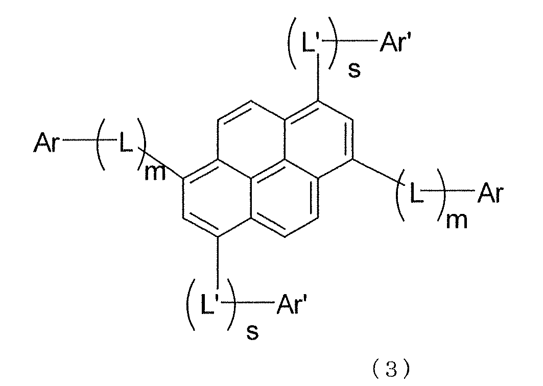
- the asymmetric pyrene derivative of the present invention is preferably the compounds represented by a following general formula (3).
- Ar, Ar', L, L', m and s are the same with the aforementioned, and preferable examples thereof and examples of the substituent thereof are the same with aforementioned.
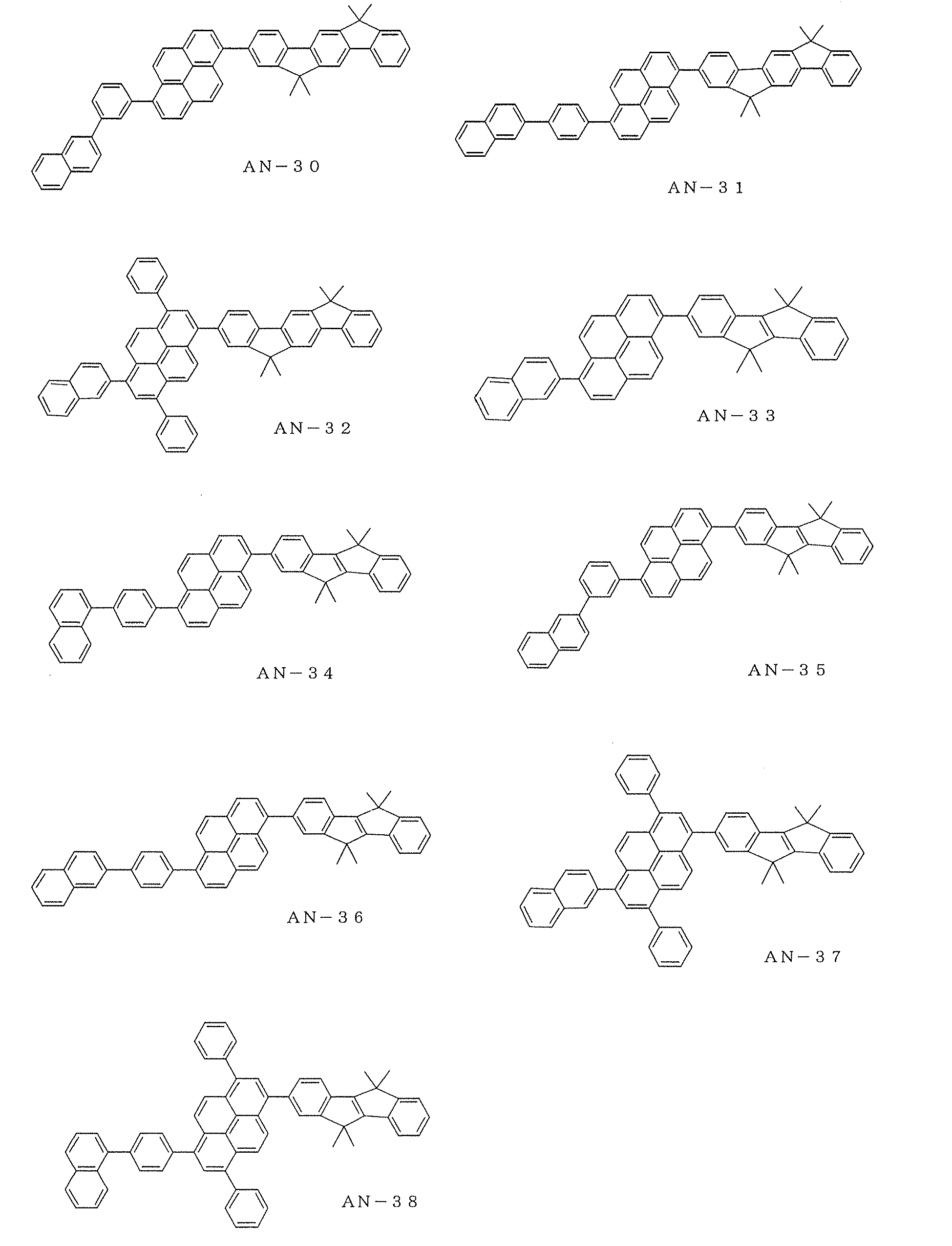
- asymmetric pyrene derivatives represented by the general formulae (1) to (3) of the present invention include the following compounds, though not limited thereto.
- the reaction solvent includes water, aromatic hydrocarbons such as benzene, toluene and xylene, ether such as 1,2-dimethoxyethane, diethyl-ether, methyl-t-butylether, tetrahydrofuran, and dioxane, saturated hydrocarbon such as pentane, hexane, heptane, octane and cyclohexane, halogenated hydrocarbon such as dichloromethane, chloroform, carbon tetrachloride, 1,2-dichloroethane and 1,1,1-trichloroethane, nitrile such as acetonitrile and benzonitrile, ester such as ethylacetate, methylacetate and butylacetate, amide such as N,N-dimethylformamide, N,N-dimethylacetoamide and N-methylpyrrolidone, and the solvent may be used singly or in combination of two or more kind thereof.
- an amount of the solvent is from 3 to 50 fold by weight, preferably 4 to 20 fold by weight to an aryl-boronic acid and a derivative thereof (or a pyrenyl-boronic acid and a derivative thereof).
- a base to be used for the reaction includes, for example, sodium carbonate, potassium carbonate, sodium hydroxide, potassium hydroxide, sodium bicarbonate, potassium bicarbonate, magnesium carbonate, lithium carbonate, potassium fluoride, cesium fluoride, cesium chloride, cesium bromide, cesium carbonate, potassium phosphate, sodium methoxide, potassium t-butoxide, sodium t-butoxide and lithium t-butoxide, and sodium carbonate is preferred.
- An amount of the base to be used is generally from 0.7 to 10 mole in equivalence, preferably from 0.9 to 6 mole in equivalence to an aryl-boronic acid and a derivatives thereof (or a pyrenyl-boronic acid and a derivative thereof).
- Catalysts to be used for the reaction include, for example, a palladium catalyst such as tetrakis(triphenylphosphine)palladium, dichlorobis(triphenylphosphine)palladium, dichloro[bis(diphenylphosphine) ethane]palladium, dichloro[bis(diphenylphosphine)propane]palladium, dichloro[bis(diphenylphosphine)butane]palladium, dichloro[bis(diphenylphosphine) ferrocene]palladium, and a nickel catalyst such as tetrakis(triphenylphosphine) nickel, dichlorobis(triphenylphosphine)nickel, dichloro[bis(diphenylphosphine) ethane]nickel, dichloro[bis(diphenylphosphine)propane]nickel, dichloro[bis (dipheny
- the tetrakis(triphenylphosphine)palladium is preferred.
- An amount of the catalysts to be used is generally from 0.001 to 1 mole in equivalence, preferably from 0.01 to 0.1 mole in equivalence to an anthracene derivative halide.
- Halogen of pyrene halide compounds and aryl halide compounds includes iodine atom, bromine atom, chlorine atom and so forth, and iodine atom and bromine atom are preferred.
- a halogenation reagent for halogenation is not limited, for example, N-succinic acid imide halide is in particular preferably to be used.
- An amount of the halogenation reagent to be used is generally from 0.8 to 10 mole in equivalence, preferably from 1 to 5 mole in equivalence to a base material.
- the reaction is carried out generally in an inert solvent under inert atmosphere such as nitrogen, argon, helium.
- the inert solvents to be used include N,N-dimethylformamide, N,N-dimethylacetamide, N-methyl pyrrolidone, dimethyl sulfoxide, carbon tetrachloride, chlorobenzene, dichlorobenzene, nitrobenzene, toluene, xylene methyl cellosolve, ethyl cellosolve, water and the like, and N,N-dimethylformamide and N-methyl pyrrolidone are preferred.
- An amount of the solvent to be used is generally from 3 to 50 fold by weight, preferably from 5 to 20 fold by weight to a base material.
- the reaction temperature is generally from 0 to 200°C, preferably from 20 to 120°C.
- the esterification by boric acid may be carried out in accordance with known methods ( Japan Chemical Society' editorial, The Experimental Chemistry Course No.4 edition,Vol 24, 61-90 ; J. Org. Chem., Vol.60, 7508 , etc.).
- the esterification by boric acid is carried out generally under inert atmosphere such as nitrogen, argon, helium and by using an inert solvent as a reaction solvent.
- the solvents include, for example, saturated hydrocarbon such as pentane, hexane, heptane, octane and cyclohexane, ether such as 1,2-dimethoxyethane, diethylether, methyl-t-butylether, tetrahydrofuran and dioxane, aromatic hydrocarbon such as benzene, toluene and xylene. These may be used singly or as mixture thereof, and dimethylether and toluene are preferred.
- An amount of the solvent to be used is generally from 3 to 50 fold by weight, preferably from 4 to 20 fold by weight to an arylhalide compound.
- the lithiation reagent to be used includes, for example, alkyl metal reagent such as n-butyllithium, t-butyllithium, phenyllithium and methyllithium, amido-base such as lithium di-isopropylamide and lithiumbistrimethylsilylamide, and n-butyllithium is preferred.
- alkyl metal reagent such as n-butyllithium, t-butyllithium, phenyllithium and methyllithium
- amido-base such as lithium di-isopropylamide and lithiumbistrimethylsilylamide
- n-butyllithium is preferred.
- Grignard reagent may be prepared by reacting an arylhalide compound (or a pyrenylhalide compound) and a magnesium metal.
- Trialkyl borate to be used includes trimethyl borate, triethyl borate, tri-isopropyl borate, tri-isobutyl borate and the like, and trimethyl borate and tri-isopropyl borate are preferred.
- Each amount of the lithiation reagent and the magnesium metal to be used is generally from 1 to 10 mole in equivalence, preferably from 1 to 2 mole in equivalence respectively to an arylhalide compound (or a pyrenylhalide compound).
- An amount of trialkyl borate to be used is generally from 1 to 10 mole in equivalence, preferably from 1 to 5 mole in in equivalence to an arylhalide compound (or a pyrenylhalide compound).
- the reaction temperature is from -100 to 50°C, in particular preferably from -75 to 10°C.
- the asymmetric pyrene derivatives of the present invention are preferred for a light emitting material of the organic EL device, and particularly preferred for a host material of the organic EL device.
- An organic EL device of the present invention comprises at least one organic thin film layer including a light emitting layer sandwiched between a pair of electrode consisting of an anode and a cathode, wherein the organic thin film layer comprises at least one kind selected from the asymmetric pyrene derivatives represented by the aforementioned general formulae (1) to (3) singly or as a component of mixture thereof,.
- the organic EL device of the present invention is preferred when the aforementioned light emitting layer comprises further an arylamine compound and/or a styrylamine compound.
- the preferred styrylamine compounds are shown by the following general formula (4):
- Ar 2 represents a group selected from among a phenyl group, a biphenyl group, a terphenyl group, a stilbene group and a distyryl aryl group;
- Ar 3 and Ar 4 each independently represents a hydrogen atom or an aromatic group having 6 to 20 carbon atoms; further Ar 2 , Ar 3 and Ar 4 each may be substituted;
- p represents an integer of 1 to 4; and more preferably, at least one of Ar 3 and Ar 4 is substituted with a styryl group.
- the aromatic group having 6 to 20 carbon atoms includes a phenyl group, a naphthyl group, an anthranyl group, a phenanthryl group, a terphenyl group or the like.
- the preferred arylamine compounds are represented by the general formula (5):
- Ar 5 to Ar 7 each independently represents an aryl group having 5 to 40 ring carbon atoms that may be substituted, and q represents an integer of 1 to 4.
- the aryl group having 5 to 40 ring carbon atoms includes a phenyl group, a naphthyl group, chrysenyl group, a naphthacenyl group, an anthranil group, a phenanthryl group, a pyrenyl group, a coronyl group, a biphenyl group, a terphenyl group, a pyrrolyl group, a furanyl group, a thiophenyl group, a benz thiophenyl group, an oxadiazolyl group, a diphenyl anthranil group, an indolyl group, a carbazolyl group, a pyridyl group, a benz quinolyl group, a fluoranthenyl group, an acenaphthofluoranthenyl group, a stilbene group or so.
- the aryl group having 5 to 40 carbon atoms may be further substituted with a substituent, and preferable examples of the substituent include an alkyl group having 1 to 6 carbon atoms (an ethyl group, a methyl group, an i-propyl group, a n-propyl group, a s-butyl group, a t-butyl group, a pentyl group, a hexyl group, a cyclopentyl group, a cyclohexyl group, etc.), an alkoxy group having 1 to 6 carbon atoms (an ethoxy group, a methoxy group, an i-propoxy group, a n-propoxy group, a s- butoxy group, a t-butoxy group, a pentoxy group, a hexyloxy group, a cyclo pentoxy group, a cyclohexyl oxy group, etc.), an aryl group having
- Typical examples of the construction of the organic EL device of the present invention include:
- the organic EL device is produced on a substrate which transmits light. It is preferable that the substrate which transmits light has a transmittance of light of 50% or greater in the visible region of 400 to 700 nm. It is also preferable that a flat and smooth substrate is employed.
- the substrate which transmits light for example, glass sheet and synthetic resin sheet are advantageously employed.
- the glass sheet include soda ash glass, glass containing barium and strontium, lead glass, aluminosilicate glass, borosilicate glass, barium borosilicate glass and quartz.
- specific examples of the synthetic resin sheet include sheet made of polycarbonate resins, acrylic resins, polyethylene terephthalate resins, polyether sulfide resins and polysulfone resins.
- the anode in the organic EL device of the present invention covers a role of injecting holes into a hole transport layer or into a light emitting layer, and it is effective that the anode has a work function of 4.5 eV or greater.
- Specific examples of the material for the anode include indium tin oxide alloy (ITO), tin oxide (NESA), gold, silver, platinum, copper, etc.
- ITO indium tin oxide alloy
- NESA tin oxide
- gold silver, platinum, copper, etc.
- the cathode its material preferably has a small work function with the aim of injecting electrons into an electron transport layer or into a light emitting layer.
- the anode can be prepared by forming a thin film of the electrode material described above in accordance with a process such as a vapor deposition process or a sputtering process.
- the anode When the light emitted from the light emitting layer is observed through the anode, it is preferable that the anode has a transmittance of the emitted light greater than 10 %. It is also preferable that the sheet resistivity of the anode is several hundred ⁇ / ⁇ or smaller.
- the thickness of the anode is, in general, selected in the range of from 10 nm to 1 ⁇ m and preferably in the range of from 10 to 200 nm.
- the light emitting layer has the following functions:
- the hole injecting layer and the hole transporting layer are layers which assist injection of holes into the light emitting layer and transport the holes to the light emitting zone.
- the layers exhibit a great mobility of holes and, in general, have an ionization energy as small as 5.5 eV or smaller.
- a material which transports holes to the light emitting layer at a small strength of the electric field is preferable.
- a material which exhibits, for example, a mobility of holes of at least 10 -4 cm 2 /V ⁇ sec under application of an electric field of from 10 4 to 10 6 V/cm is preferable.
- any arbitrary material selected from conventional material commonly used as a charge transporting material for the holes in photoconduction materials and well known material employed for the hole injecting layer in the EL device is usable.
- Further examples include triazole derivatives (refer to U. S. Patent No. 3,112,197 , etc.), oxadiazole derivatives (refer to U. S. Patent No. 3,189,447 , etc.), imidazole derivatives (refer to Japanese Examined Patent KOKOKU No. Shou 37-16096 , etc.), polyarylalkane derivatives (refer to United States Patent Nos. 3,615,402 , 3,820,989 and 3,542,544 , Japanese Examined Patent KOKOKU Nos. Shou 45-555 and Shou 51-10983 , Japanese Unexamined Patent Application Laid-Open Nos.
- Hei 2-282263 an electroconductive polymer oligomer which is disclosed in Japanese Unexamined Patent Application Laid-Open No Hei 1-211399 (particularly, thiophene oligomer), etc.
- the above materials are also employable, however, porphyrin compounds, aromatic tertiary amine compounds and styryl amine compounds (refer to U.S Patent No. 4,127,412 , Japanese Unexamined Patent Application Laid-Open Nos.
- inorganic compound such as p-type silicon, p-type silicon carbide or so is employable as the material for the hole injecting layer.
- a thin film may be formed from the material for the hole injecting layer or the hole transporting layer, respectively, in accordance with a well known process such as the vacuum vapor deposition process, the spin coating process, the casting process and the LB process.
- the thickness of the hole injecting layer and the hole transporting layer is not particularly limited, the thickness is usually from 5 nm to 5 ⁇ m.
- the organic semiconductor layer assists to inject the holes or to inject the electrons into the light emitting layer, and it is preferable for the organic semiconductor layer to have a electric conductivity of 10 -10 S/cm or greater.
- electroconductive oligomers such as an oligomer having thiophene, an oligomer having arylamine disclosed in Japanese Patent Application Laid-Open No. Heisei 8(1996)-193191 and so on, electroconductive dendrimers such as a dendrimer having an arylamine and so on are employable.
- the electron injection layer in the organic EL device of the present invention is a layer which assists injection of electrons into the light emitting layer and exhibits a great mobility of electrons.
- an adhesion improving layer is a layer made of a material exhibiting excellent adhesion with the cathode. Further, it has been known that interference between luminescence directly coming from an anode and luminescence coming through reflection by an electrode is caused since a light emitted in an organic EL device is reflected by an electrode (in this case, a cathode). In order to utilize the interference effect efficiently, a thickness of an electron transferring layer is selected from the range of several nm to several ⁇ m accordingly.
- an electron mobility is at least 10 -5 cm 2 /Vs or more when an electric field of from 10 4 to 10 6 V/cm is applied.
- 8-hydroxyquinoline, metal complexes of derivatives thereof and oxadiazole derivatives are preferable.
- the 8-hydroxyquinoline and metal complexes of derivatives thereof include metal chelates of oxinoid compounds including chelates of oxine (in general, 8-quinolinol or 8-hydroxyquinoline).
- tris(8-quinolinol)aluminum (Alq) can be employed as the electron injecting material.
- examples of the oxadiazole deliveries include an electron transfer compound shown as the following general formulae: wherein Ar 1 , Ar 2 , Ar 3 , Ar 5 , Ar 6 and Ar 9 each independently represents a substituted or unsubstituted aryl group, which may be the same with or different from each other; Ar 4 , Ar 7 and Ar 8 each independently represents a substituted or unsubstituted arylene group, which may be the same with or different from each other.
- the aryl group include a phenyl group, a biphenyl group, an anthranil group, a perilenyl group and a pyrenyl group.
- examples of the arylene group include a phenylene group, a naphthylene group, a biphenylene group, an anthranylene group, a perilenylene group, a pyrenylene group, etc.
- examples of the substituent include an alkyl group having 1 to 10 carbon atoms, an alkoxy group or a cyano group each having 1 to 10 carbon atoms respectively, etc.
- the electron transfer compound those compounds having a thin film forming capability are preferable.
- a material to be used for an electron injecting layer and an electron transferring layer includes any of compounds represented by the following general formulae (A) to (G).
- a 1 to A 3 each independently represents nitrogen atom or carbon atom.
- Ar 1 represents a substituted or unsubstituted aryl group having 6 to 60 ring carbon atoms, or a substituted or unsubstituted hetero aryl group having 3 to 60 ring carbon atoms
- Ar 2 represents a hydrogen atom, a substituted or unsubstituted aryl group having 6 to 60 ring carbon atoms, or a substituted or unsubstituted hetero aryl group having 3 to 60 ring carbon atoms, a substituted or unsubstituted alkyl group having 1 to 20 carbon atoms, or a substituted or unsubstituted alkoxy group having 1 to 20 carbon atoms, or a bivalent group of these;
- Ar 1 or Ar 2 is, however, a substituted or unsubstituted condensed ring group having 10 to 60 ring carbon atoms or a substituted or unsubstituted
- L 1 , L 2 and L each independently represents a single bond, a substituted or unsubstituted arylene group having 6 to 60 ring carbon atoms, a substituted or unsubstituted hetero arylene group having 3 to 60 ring carbon atoms, or a substituted or unsubstituted fluorene group.
- R represents hydrogen, a substituted or unsubstituted aryl group having 6 to 60 ring carbon atoms, or a substituted or unsubstituted hetero aryl group having 3 to 60 ring carbon atoms, a substituted or unsubstituted alkyl group having 1 to 20 carbon atoms, or a substituted or unsubstituted alkoxy group having 1 to 20 carbon atoms.
- n represents an integer of from 0 to 5
- a plural number of R, if any, may be either the same with or different from each other when n is 2.
- a plural number of R, if any, when these are adjacent to each other may be bonded each other to form a carbocyclic aliphatic ring or a carbocyclic aromatic ring.
- HAr represents a nitrogen-containing heterocyclic derivative and further may have a substituent, having 3 to 40 of carbon atoms
- L represents a single bond
- Ar 1 represents a bivalent aromatic hydrocarbon group and further may have a substituent, having 6 to 60 carbon atoms
- Ar 2 represents an aryl group and further may have a substituent, having 6 to 60 carbon atoms or a hetero aryl group and further may have a substituent, having 3 to 60 carbon atoms, represents a nitrogen-containing heterocyclic derivative.
- X and Y each independently represents a substituted or unsubstituted hydrocarbon group having 1 to 6 of carbon atoms, an alkoxy group, an alkenyloxy group, an alkynyloxy group, a hydroxyl group, a substituted or unsubstituted aryl group, a substituted or unsubstituted hetero ring, or a structure forming a saturated or unsaturated ring by bonding X and Y, of R 1 to R 4 each represents independently a hydrogen atom, a halogen atom, a substituted or unsubstituted alkyl group having 1 to 6 carbon atoms, an alkoxy group, an aryloxy group, a perfuluoroalkyl group, a perfuluoroalkoxy group, an amino group, an alkylcarbonyl group, an arylcarbonyl group, an alkoxycarbonyl group, an aryloxycarbonyl group, an azo group, an
- R 1 to R 8 and Z 2 each independently represents a hydrogen atom, a saturated or unsaturated hydrocarbon, an aromatic group, an heterocyclic group, a substituted amino group, a substituted boryl group, an alkoxy group or an aryloxy group
- each of X, Y and Z 1 represents independently a saturated or unsaturated hydrocarbon, an aromatic group, an heterocyclic group, a substituted amino group, an alkoxy group or an aryloxy group
- substitutes of Z 1 and Z 2 may bond each other to form a condesed ring
- n represents an integer of 1 to 3
- Z 1 may be different from each other when n is 2 or more; any compound, however, of which n is 1, X, Y and R 2 are methyl groups
- R 8 is a hydrogen atom or a substituted boryl group, or, of which n is 3 and Z 1 is a methyl group, is excluded.
- Q 1 and Q 2 each independently represents a ligand shown by the general formula (G)
- L represents a ligand shown by a halogen atom, a substituted or unsubstituted alkyl group, a substituted or unsubstituted cycloalkyl group, a substituted or unsubstituted aryl group, heterocyclic group, - OR 1
- R 1 represents a hydrogen atom, a substituted or unsubstituted alkyl group, a substituted or unsubstituted cycloalkyl group, a substituted or unsubstituted aryl group, or a substituted or unsubstituted heterocyclic group or -O-Ga-Q 3 (Q 4 ) (Q 3 and Q 4 are the same with Q 1 and Q 2 ).
- rings A 1 and A 2 have a six-member aryl-ring structure and further may have a substituent, formed by condensing each other.
- the metal complex shows a strong property as a n-type impurity semiconductor so that a capability of electron injection is significant.
- affinity between the metal complex formed and the ligand is strong so that fluorescent quantum efficiency for a light emitting material is increased.
- the specific examples of a substituent for A 1 and A 2 forming a ligand of the general formula (G) include a halogen atom of halogen, bromine and iodine, a substituted or unsubstituted alkyl group such as a methyl group, a ethyl group, a propyl group, a butyl group, a sec-butyl group, a tert-butyl group, a pentyl group, a hexyl group, a heptyl group, an octyl group, a stearyl group and trichloromethyl group, a substituted or unsubstituted aryl group such as a phenyl group,
- a reductive dopant is added in either the electron transporting zone or an interfacial zone between the cathode and the organic layer.
- the reductive dopant used in the present invention is defined as a substance which reduces the electron transporting compound.
- the reductive dopant include at least one compound selected from alkali metals, alkali metallic complexes, alkali metal compounds, alkaline earth metals, alkaline earth metallic complexes, alkaline earth metal compounds, rare earth metals, rare earth metallic complexes and rare earth metal compounds.
- Examples of the preferable reductive dopant include at least one alkali metal selected from a group consisting of Li (the work function: 2.93 ev), Na (the work function: 2.36 eV), K (the work function: 2.28 eV), Rb (the work function: 2.16 eV) and Cs (the work function: 1.95 eV) or at least one alkaline earth metals selected from a group consisting of Ca (the work function: 2.9eV), Sr (the work function: 2.0 to 2.5 eV) and Ba (the work function: 2.52eV); whose work function of 2.9 eV or smaller is particularly preferable.
- Li the work function: 2.93 ev
- Na the work function: 2.36 eV
- K the work function: 2.28 eV
- Rb the work function: 2.16 eV
- Cs the work function: 1.95 eV
- alkaline earth metals selected from a group consisting of Ca (the work function: 2.9eV), Sr (
- the preferable reductive dopant include at least one alkali metal selected from a group consisting of K, Rb and Cs, the more preferred is Rb or Cs, and the most preferred is Cs.
- alkali metals have particularly high ability of reduction so that improvement of an emission luminance and longer lasting of a lifetime of the organic EL device may be realized.
- a combination of two or more of alkali metals is also preferable as a reductive dopant having 2.9 eV or less of the work function.
- a combination of Cs for example with Na, Cs, K or Rb, or Na and K is preferable.
- an electron injecting layer formed with an insulating material or a semiconductor may be further sandwiched between the cathode and the organic thin film layer.
- the electron injecting layer effectively prevents leak in the electric current and improves the electron injecting capability.
- at least one metal compound selected from the group consisting of alkali metal chalcogenides, alkaline earth metal chalcogenides, alkali metal halides and alkaline earth metal halides is used as the insulating material.It is preferable that the electron injecting layer is constituted with the above alkali metal chalcogenide since the electron injecting property can be improved.
- Preferable examples of the alkali metal chalcogenide include Li 2 O, LiO, Na 2 S, Na 2 Se and NaO.
- Preferable examples of the alkaline earth metal chalcogenide include CaO, BaO, SrO, BeO, BaS and CaSe.
- Preferable examples of the alkali metal halide include LiF, NaF, KF, LiCl, KCl and NaCl.
- Preferable examples of the alkaline earth metal halide include fluorides such as CaF 2 , BaF 2 , SrF 2 , MgF 2 and BeF 2 and halides other than the fluorides.
- the semiconductor constituting the electron transporting layer examples include oxides, nitrides and nitriding oxides containing at least one element selected from Ba, Ca, Sr, Yb, Al, Ga, In, Li, Na, Cd, Mg, Si, Ta, Sb and Zn, which are used singly or in combination of two or more. It is preferable that the inorganic compound constituting the electron transporting layer is in the form of a fine crystalline or amorphous insulating thin film When the electron transporting layer is constituted with the above insulating thin film, a more uniform thin film can be formed and defective pixels such as dark spots can be decreased.
- the inorganic compound include the alkali metal chalcogenides, the alkaline earth metal chalcogenides, the alkali metal halides and the alkaline earth metal halides which are described above.
- an electrode substance such as metal, alloy, electroconductive compound and those mixture having a small work function (4 eV or smaller) is employed.
- the electrode substance include potassium, sodium- potassium alloy, magnesium, lithium, magnesium-silver alloy, aluminum / aluminum oxide, aluminum-lithium alloy, indium, rare earth metal, etc.
- the cathode can be prepared by forming a thin film of the electrode material described above in accordance with a process such as the vapor deposition process and the sputtering process. When the light emitted from the light emitting layer is observed through the cathode, it is preferable that the cathode has a transmittance of the emitted light greater than 10 %.
- the sheet resistivity of the cathode is several hundred ⁇ / ⁇ or smaller.
- the thickness of the cathode is, in general, selected in the range of from 10 nm to 1 ⁇ m and preferably in the range of from 50 to 200 nm.
- an organic EL device tends to form defects in pixels due to leak and short circuit since an electric field is applied to ultra-thin films.
- a layer of an insulating thin film may be inserted between the pair of electrodes.
- the material employed for the insulating layer include aluminum oxide, lithium fluoride, lithium oxide, cesium fluoride, cesium oxide, magnesium oxide, magnesium fluoride, calcium oxide, calcium fluoride, aluminum nitride, titanium oxide, silicon oxide, germanium oxide, silicon nitride, boron nitride, molybdenum oxide, ruthenium oxide and vanadium oxide. Mixtures and laminates of the above compounds can also be employed.
- an organic EL device of the present invention for example, a cathode, a light emitting layer and, where necessary, a hole injecting layer and an electron injecting layer are formed in accordance with the aforementioned process using the aforementioned materials, and the anode is formed in the last step.
- An organic EL device may be produced by forming the aforementioned layers in the order reverse to that described above, i.e., an anode being formed in the first step and a cathode in the last step.
- An embodiment of the process for producing an organic EL device having a construction in which a cathode, a hole injecting layer, a light emitting layer, an electron injecting layer and an anode are disposed sequentially on a light-transmitting substrate will be described in the following.
- a thin film made of a material for the cathode is formed in accordance with the vapor deposition process or the sputtering process so that the thickness of the formed thin film is 1 ⁇ m or smaller and preferably in the range of 10 to 200 nm.
- the formed thin film is employed as the cathode.
- a hole injecting layer is formed on the cathode.
- the hole injecting layer can be formed in accordance with the vacuum vapor deposition process, the spin coating process, the casting process or the LB process, as described above.
- the vacuum vapor deposition process is preferable since a uniform film can be easily obtained and the possibility of formation of pin holes is small.
- the conditions in general are suitably selected in the following ranges: temperature of the deposition source: 50 to 450°C; vacuum level: 10 -7 to 10 -3 Torr; deposition rate: 0.01 to 50 nm/second; temperature of the substrate: -50 to 300°C; and film thickness: 5 nm to 5 ⁇ m; although the conditions of the vacuum vapor deposition are different depending on the employed compound (the material for the hole injecting layer) and the crystal structure and the recombination structure of the hole injecting layer to be formed.
- the light-emitting layer is formed on the hole-injecting layer formed above.
- the formation of the light emitting layer can be made by forming the light emitting material according to the present invention into a thin film in accordance with the vacuum vapor deposition process, the sputtering process, the spin coating process or the casting process.
- the vacuum vapor deposition process is preferable because a uniform film can be easily obtained and the possibility of formation of pinholes is small.
- the conditions of the vacuum vapor deposition process can be selected in the same ranges as those described for the vacuum vapor deposition of the hole-injecting layer although the conditions are different depending on the used compound. It is preferable that the thickness is in the range of from 10 to 40 nm.
- the electron-injecting layer is formed on the light-emitting layer formed above. Similarly to the hole injecting layer and the light-emitting layer, it is preferable that the electron-injecting layer is formed in accordance with the vacuum vapor deposition process since a uniform film must be obtained.
- the conditions of the vacuum vapor deposition can be selected in the same ranges as those for the hole injecting layer and the light-emitting layer.
- the anode is formed on the electron injecting layer, and an organic EL device can be fabricated.
- the anode is made of a metal and can be formed in accordance with the vacuum vapor deposition process or the sputtering process.
- the vacuum vapor deposition process is employed in order to prevent the lower organic layers from damages during the formation of the film.
- the above layers from the anode to the cathode are formed successively while the production system is kept in a vacuum after being evacuated.
- the process for forming the layers in the organic EL device of the present invention is not particularly limited.
- a conventional process such as the vacuum vapor deposition process and the spin coating process can be used.
- the organic thin film layer comprising the compound having a spiro bond represented by the foregoing general formula (1) used in the organic EL device of the present invention can be formed in accordance with the vacuum vapor deposition process, the molecular beam epitaxy process (the MBE process) or, using a solution prepared by dissolving the compound into a solvent, in accordance with a conventional coating process such as the dipping process, the spin coating process, the casting process, the bar coating process and the roller coating process.
- each layer in the organic thin film layer in the organic EL device of the present invention is not particularly limited, therefore, a thickness within the range of several nanometers to 1 ⁇ m is preferable so as to reduce the defects such as pin holes and improve the efficiency.
- the uniform light emission is observed only in the condition that the polarity of the cathode is positive and the polarity of the anode is negative.
- any type of wave shape can be employed.
- the organic layer was washed by saturated salt water, followed by drying through anhydrous sodium sulfate, and then the organic solvent was removed by an evaporator.
- the residue was refined through a silica gel chromatography (a developing solvent: toluene) and then 10.0 g of 1-(4-naphthalene-1-yl-phenyl) pyrene was obtained. (yield: 99 %) 10.0 g of 1-(4-naphthalene-1-yl-phenyl)pyrene obtained was dispersed into 100 ml of dimethyl formaldehyde (DMF), and 5.3 g N-bromosuccinamide (NBS) in DMF solution was dropped therein at room temperature.
- DMF dimethyl formaldehyde
- NBS N-bromosuccinamide
- the organic layer was washed by saturated salt water, followed by drying through anhydrous sodium sulfate, and then the organic solvent was removed by an evaporator.
- the measurement result of the compound by FD-MS Field Desorption Mass Spectrometry analysis
- the organic layer was washed by saturated salt water, followed by drying through anhydrous sodium sulfate, and then the organic solvent was removed by an evaporator.
- 1-naphthalene boronic acid in place of 4-(naphthalene-1-yl)phenyl boronic acid was used in Synthesis Example 1 (1), and then 1-bromo-6-(naphthalene-1-yl) pyrene and 1-bromo-8-(naphthalene-1-yl) pyrene were obtained.
- the organic layer was washed by saturated salt water, followed by drying through anhydrous sodium sulfate, and then the organic solvent was removed by an evaporator.
- 7.1 g of diiodo-9,9'-dimetyl-7-naphthalene-1-yl-9H-fluorene obtained and 4.7 g of 1-pyrene boronic acid were dissolved in 100 ml of DME.
- Example 1 ((Fabrication of an organic EL device)
- a glass substrate manufactured by GEOMATEC Company of 25 mm ⁇ 75 mm ⁇ 1.1 mm thickness having an ITO transparent electrode was cleaned by application of ultrasonic wave in isopropyl alcohol for 5 minutes and then by exposure to ozone generated by ultraviolet light for 30 minutes.
- the cleaned glass substrate having an ITO transparent electrode line was fixed to a substrate holder of a vacuum deposition apparatus, and on the surface, where the ITO transparent electrode line was fixed, of the substrate, a film (hereinafter referred to as TPD232 film) having film thickness of 60 nm of the following N,N'-bis(N,N'-diphenyl-4-aminophenyl)-N,N-diphenyl-4,4'-diamino-1,1'-biphel was formed so as to cover the transparent electrode.
- the TPD232 film performs as a hole injecting layer.
- TBDB layer a layer having layer thickness of 20 nm of the following N,N,N',N'-tetra(4-biphenyl)-diaminobiphenylene was formed (hereinafter referred to as TBDB layer).
- the layer performs as a hole transporting layer.
- a film having a film thickness of 40 nm of the aforementioned compound AN-2 was formed as host material by a vapor deposition.
- the following amino compound BD1 containing a styryl group was deposited at the ratio by weight between AN-2 and BD 1 of 40: 3 by a vapor deposition. The film performs as a light emitting layer.
- a film having a Alq film thickness of 10 nm was formed on the film.
- the film performs as an electron injecting layer.
- a film (film thickness: 10 nm) of Alq : Li (the source of lithium: manufactured by SAES GETTERS Company) as an electron injecting layer was formed by binary vapor deposition of Li as a reductive dopant and the following Alq.
- Alq : Li film Al metal was deposited to form a metal cathode, therefore, an organic EL device was fabricated.
- the device was tested by passing electric current, an emission luminance of 615 cd/m 2 and a current efficiency of 6.5cd/Awas observed at a voltage of 5.76V and a current density of 10mA/cm 2 .
- the results of the half-lifetime are shown in Table 1.
- Organic EL devices were fabricated similar to Example 1 except that the compounds described in Table 1 were used in place of the compound (AN-2). The devices obtained were tested by passing electric current similar to the example 1, the results of the half-lifetime measured at an initial luminance of 1,000cd/m 2 , are shown in Table 1.
- Organic EL devices were fabricated similar to the example 1 except that the following compounds an-1 (Comparative Example 1), an-2 (Comparative Example 2) and an-3 (Comparative Example 3) were used in place of the compound (AN-2).
- the devices obtained were tested by passing electric current similar to the example 1, the results of the half-lifetime measured at an initial luminance of 1,000cd/m 2 , were described in Table 1.
- an organic EL device employing a compound having an asymmetric pyrene derivative of the present invention exhibits a great efficiency of light emission and has a long lifetime. Therefore, they are highly applicable as the organic EL devices supposed to be used continuously for long years.
Abstract
Description
- The present invention relates to an asymmetric pyrene derivative and an organic electroluminescence ("electroluminescence" will be occasionally referred to as "EL", hereinafter) device employing the same, more particularly, to an organic EL device exhibiting a great efficiency of light emission and having a long lifetime, and also to the asymmetric pyrene derivative for realizing the organic EL device.
- An organic electroluminescence device is a spontaneous light emitting device which utilizes the principle that a fluorescent substance emits light by energy of recombination of holes injected from an anode and electrons injected from a cathode when an electric field is applied. Since an organic EL device of the laminate type driven under a low electric voltage was reported by C. W. Tang et al. of Eastman Kodak Company (C. W. Tang and S. A. Vanslyke, Applied Physics Letters, Volume 51, Pages 913, 1987), many studies have been conducted on organic EL devices using organic materials as the constituting materials. Tang et al. used a laminate structure using tris(8-hydroxyquinolinol aluminum) for the light emitting layer and a triphenyldiamine derivative for the hole transporting layer. Advantages of the laminate structure are that the efficiency of hole injection into the light emitting layer can be increased, that the efficiency of forming excited particles which are formed by blocking and recombining electrons injected from the cathode can be increased, and that excited particles formed among the light emitting layer can be enclosed. As the structure of the organic EL device, a two-layered structure having a hole transporting (injecting) layer and an electron transporting and light emitting layer and a three-layered structure having a hole transporting (injecting) layer, a light emitting layer and an electron transporting (injecting) layer are well known. To increase the efficiency of recombination of injected holes and electrons in the devices of the laminate type, the structure of the device and the process for forming the device have been studied.
- As the light emitting material of the organic EL device, chelate complexes such as tris(8-quinohnolato)aluminum, coumarine derivatives, tetraphenylbutadiene derivatives, bisstyrylarylene derivatives and oxadiazole derivatives are known. It is reported that light in the visible region ranging from blue light to red light can be obtained by using these light emitting materials, and development of a device exhibiting color images is expected (refer to, for example, Patent literature 1, Patent literature 2, and Patent literature 3).
Further, a device using asymmetrical pyrene derivative as the light emitting material is disclosed in Patent literatures 4 to 7, and a device using an asymmetrical anthracene derivative as the light emitting material is disclosed in Patent literature 8. Although these derivatives are used as the material for emitting blue light, further improvements of the lifetime thereof have been desired. In addition, development of a derivative being not easily affected by oxidization has been desired because of low oxidative stability of existing derivatives. -
- Patent literature 1:
-
Japanese Patent Application Laid-Open No. Heisei 8(1996)-239655 - Patent literature 2:
-
Japanese Patent Application Laid-Open No. Heisei 7(1995)-138561 - Patent literature 3:
-
Japanese Patent Application Laid-Open No. Heisei 3(1991)-200289 - Patent literature 4:
-
Japanese Patent Application Laid-Open No. 2001-118682 - Patent literature 5:
-
Japanese Patent Application Laid-Open No. 2002-63988 - Patent literature 6:
-
Japanese Patent Application Laid-Open No. 2004-75567 - Patent literature 7:
-
Japanese Patent Application Laid-Open No. 2004-83481 - Patent literature 8:
- International PCT publication No.
WO 04/018587 - The present invention has been made to overcome the above problems and has an objective of providing an organic electroluminescence device exhibiting a great efficiency of light emission and having a long lifetime, and also to an asymmetric pyrene derivative for realizing the organic EL device.
- As a result of intensive researches and studies to achieve the above objective by the present inventors, it was found that employing an asymmetric derivative represented by any of following general formulae from (1) to (3) as a constituting material for an organic thin film of an organic EL device enables to provide the organic EL device exhibiting a great efficiency of light emission and having a long lifetime.
- Therefore, the present invention provides an asymmetric pyrene derivative represented by any of the following general formulae (1) to (3):

- In the general formula (1), Ar and Ar' each represents a substituted or unsubstituted aromatic group having 6 to 50 ring carbon atoms;
L and L' each represents a substituted or unsubstituted phenylene group, a substituted or unsubstituted naphthalenylene group, a substituted or unsubstituted fluorenylene group or a substituted or unsubstituted dibenzosilolylene group;
m represents an integer of 0 to 2, n represents an integer of 1 to 4, s represents an integer of 0 to 2 and t represents an integer of 0 to 4; and,
L or Ar bonds to any one of 1 to 5 position of pyrene, also L' or Ar' bonds to any one of 6 to 10 position thereof,
however, when n + t is an even number, Ar, Ar', L and L' satisfy a following requirement (1) or a requirement (2): - (1) Ar ≠ Ar' and/or L ≠ L' (wherein ≠ means that each group has a different structure)
- (2) when Ar = Ar' and L = L'
- (2-1) m ≠ s and/or n ≠ t, or
- (2-2) when m = s and n = t,
- (2-2-1) both L and L' or pyrene bond respectively to a different position ofAr and Ar' or (2-2-2) both L and L' or pyrene bond respectively to the same position of Ar and Ar' excluding a case where both L and L' or both Ar and Ar' bond respectively to 1 and 6, or 2 and 7 positions thereof.
-

L' or Ar' bonds to any one of 2 to 10 positions of the pyrene, however, when t is an odd number, Ar, Ar', L and L' satisfy a following requirement (1') or a requirement (2'): - (1') Ar ≠ Ar' and/or L ≠ L' (wherein ≠ means that each group has a different structure)
- (2') when Ar = Ar' and L = L' (2-1') m ≠ s and/or t ≠ 1, or
- (2-2') when m = s and t = 1,
- (2-2-1') both L and L' or pyrene each bonds respectively to different positions of Ar and Ar', or
- (2-2-2') both L and L' or pyrene each bonds to the same positions of Ar and Ar' excluding a case where L' or Ar' bonds to 6 position thereof.
Moreover, the present invention provides an organic EL device comprising at least one organic thin film layer including a light emitting layer sandwiched between a pair of electrode consisting of an anode and a cathode, wherein the organic thin film layer comprises at least one kind selected from the aforementioned asymmetric pyrene derivatives singly or as a component of mixture thereof.
An organic EL device containing an asymmetric pyrene derivative of the present invention exhibits a great efficiency of light emission and has a long lifetime. - The present invention provides an asymmetric pyrene derivative represented by a following general formula (1):

- In the general formula (1), Ar and Ar' each represents a substituted or unsubstituted aromatic group having 6 to 50 ring carbon atoms.
Examples of the substituted or unsubstituted aromatic group include phenyl group, 1-naphthyl group, 2-naphthyl group, 1-anthryl group, 2-anthryl group, 9-anthryl group, 9-(10-phenyl) anthryl group, 9-(10-naphtyl-1-yl) anthryl group, 9-(10-naphtyl-2-yl) anthryl group, 1-phenanthryl group, 2-phenanthryl group, 3-phenanthryl group, 4-phenanthryl group, 9-phenanthryl group, 1-naphthacenyl group, 2-naphthacenyl group, 9-naphthacenyl group,1-pyrenyl group, 2-pyrenyl group, 4-pyrenyl group, 2-biphenylyl group, 3-biphenylyl group, 4-biphenylyl group, p-terphenyl-4-yl group, p-terphenyl-3-yl group, p-terphenyl-2-yl group, m-terphenyl-4-yl group, m-terphenyl-3-yl group, m-terphenyl-2-yl group, o-tolyl group, m-tolyl group, p-tolyl group, p-t-butylphenyl group, 3-methyl-2-naphthyl group, 4-methyl-1-naphthyl group, 4-methyl-1-anthryl group and the like.
Among the aforementioned, preferred examples includes phenyl group, 1-naphthyl group, 2-naphthyl group, 9-(10-phenyl) anthryl group, 9-(10-naphtyl-1-yl) anthryl group, 9-(10-naphtyl-2-yl) anthryl group, 9-phenanthryl group, 1-pyrenyl group, 2-pyrenyl group, 4-pyrenyl group, 2-biphenylyl group, 3-biphenylyl group, 4-biphenylyl group, o-tolyl group, m-tolyl group, p-tolyl group, p-t-butylphenyl group and the like. - Further, the aforementioned aromatic groups may be substituted by a substituent such as alkyl group (methyl group, ethyl group, propyl group, isopropyl group, n-butyl group, s-butyl group, isobutyl group, t-butyl group, n-pentyl group, n-hexyl group, n-heptyl group, n-octyl group, hydroxymethyl group, 1-hydroxyethyl group, 2-hydroxyethyl group, 2-hydroxyisobutyl group, 1,2-dihydroxyethyl group, 1,3-dihydroxy-isopropyl group, 2,3-dihydroxy-t-butyl group, 1,2,3-trihydroxypropyl group, chloromethyl group, 1-chloroethyl group, 2-chloroethyl group, 2-chloroisobutyl group, 1,2-dichloroethyl group, 1,3-dichloroisopropyl group, 2,3-dichloro-t-butyl group, 1,2,3-trichloropropyl group, bromomethyl group, 1-bromoethyl group, 2-bromoethyl group, 2-bromoisobutyl group, 1,2-dibromoethyl group, 1,3-dibromoisopropyl group, 2,3-dibromo-t-butyl group, 1,2,3-tribromopropyl group, iodomethyl group, 1-iodoethyl group, 2-iodoethyl group, 2-iodoisobutyl group, 1,2-diiodoethyl group, 1,3-diiodoisopropyl group, 2,3-diiodo-t-butyl group, 1,2,3-triiodopropyl group, aminomethyl group, 1-aminoethyl group, 2-aminoethyl group, 2-aminoisobutyl group, 1,2-diaminoethyl group, 1,3-diaminoisopropyl group, 2,3-diamino-t-butyl group, 1,2,3-triamino- propyl group, cyanomethyl group, 1-cyanoethyl group, 2-cyanoethyl group, 2-cyanoisobutyl group, 1,2-dicyanoethyl group, 1,3-dicyanoisopropyl group, 2,3-dicyano-t-butyl group, 1,2,3-tricyano-propyl group, nitromethyl group, 1-nitroethyl group, 2-nitroethyl group, 2-nitroisobutyl group, 1,2-dinitroethyl group, 1,3-dinitroisopropyl group, 2,3-dinitro-t-butyl group, 1,2,3-trinitropropyl group, cyclopropyl group, cyclobutyl group, cyclopentyl group, cyclohexyl group, 4-methylcyclohexyl group, 1-adamanthyl group, 2-adamanthyl group, 1-norbornyl group, 2-norbornyl group), alkoxy group having 1 to 6 carbon atoms (ethoxy group, methoxy group, i-propoxy group, n-propoxy group, s-butoxy group, t-butoxy group, pentoxy group, hexyloxy group, cyclopentoxy group, cyclohexyloxy group and etc.), aryl group having 5 to 40 ring carbon atoms, amino group substituted by aryl group having 5 to 40 ring carbon atoms, ester group containing aryl group having 5 to 40 ring carbon atoms, ester group containing alkyl group having 1 to 6 carbon atoms, cyano group, nitro group, halogen atom and the like.
- In the general formula (1), L and L' each represents a substituted or unsubstituted phenylene group, a substituted or unsubstituted naphtharenylene, a substituted or unsubstituted fluorenylene group or a substituted or unsubstituted a dibenzosilolylene group, and a substituted or unsubstituted phenylene group or a substituted or unsubstituted fluorenylene group is preferred.
In addition, the substituent thereof includes the same with the aforementioned aromatic groups.
In the general formula (1), m represents an integer of 0 to 2 (preferably 0 to 1), n represents an integer of 1 to 4 (preferably 1 to 2), s represents an integer of 0 to 2 (preferably 0 to 1) and t represents an integer of 0 to 4 (preferably 0 to 2), and, in the general formula (1), L or Ar bonds to any one of 1 to 5 positions of the pyrene, and also L' or Ar' bonds to any one of 6 to 10 positions thereof, however, when n + t is an even number, Ar, Ar', L and L' satisfy a following requirement (1) or a requirement (2): - (1) Ar ≠ Ar' and/or L = L', wherein ≠ means that each group has a different structure,
- (2) when Ar = Ar' and L = L',
- (2-1) m ≠ s and/or n ≠ t, or
- (2-2) when m = s and n = t,
- (2-2-1) both L and L' or pyrene bond respectively to a different position of Ar and Ar' or (2-2-2) both L and L' or pyrene bond respectively to the same position of Ar and Ar' excluding a case where both L and L' or both Ar and Ar' bond respectively to 1 and 6, or 2 and 7 positions thereof.
- Further, the asymmetric pyrene derivatives of the present invention include the compounds represented by a following general formula (2):

- In the general formula (2), Ar, Ar', L, L', m, s and t are the same with the aforementioned. Further, preferable examples thereof and examples of the substituent thereof are the same with aforementioned. In addition, L' or Ar' bonds to any one of 2 to 10 positions of pyrene, however, in the general formula (2), when t is an odd number, Ar, Ar', L and L' satisfy a following requirement (1') or a requirement (2');
- (1) Ar ≠ Ar' and/or L = L' , wherein ≠ means that each group has a different structure,
- (2) when Ar = Ar' and L = L',
- (2-1') m ≠ s and/or t ≠ 1, or
- (2-2') when m = s and t= 1,
- (2-2-1') both L and L' or pyrene each bonds respectively to different positions of Ar and Ar', or
- (2-2-2') both L and L' or pyrene each bonds to the same positions of Ar and Ar' excluding a case where L' or Ar' bonds to 6 position thereof.
- In addition, the asymmetric pyrene derivative of the present invention is preferably the compounds represented by a following general formula (3).
- Specific examples of the asymmetric pyrene derivatives represented by the general formulae (1) to (3) of the present invention include the following compounds, though not limited thereto.

-

-

-
- A preparation method of the asymmetric pyrene derivatives of the present invention is explained as follows:
- The asymmetric pyrene derivatives represented by the general formula (1) to (3) of the present invention and precursors thereof may be obtained by using a pyrene halide compound and an aryl-boronic acid compound, or an aryl-halide compound and pyrenyl-boronic acid compound as a starting material and applying methods such as Suzuki-coupling reaction and the like. In addition, a combination of a halogenation reaction, an esterification by boric acid and Suzuki-coupling reaction is applied to the precursor as appropriated, and then, the asymmetric pyrene derivatives represented by the general formula (1) to (3) are obtained.
- So far, many reports on Suzuki-coupling reaction have been published (Chem. Rev. Vol.954, No.7, 2457 (1995), etc.), therefore, it may be carried out in the reaction conditions described therein. The reaction is carried out generally at normal pressure in inert gas atmosphere such as nitrogen, argon, helium and the like, and also under pressurized condition as appropriated. The reaction temperature is in the range of from 15 to 300°C preferably from 30 to 200°C.
The reaction solvent includes water, aromatic hydrocarbons such as benzene, toluene and xylene, ether such as 1,2-dimethoxyethane, diethyl-ether, methyl-t-butylether, tetrahydrofuran, and dioxane, saturated hydrocarbon such as pentane, hexane, heptane, octane and cyclohexane, halogenated hydrocarbon such as dichloromethane, chloroform, carbon tetrachloride, 1,2-dichloroethane and 1,1,1-trichloroethane, nitrile such as acetonitrile and benzonitrile, ester such as ethylacetate, methylacetate and butylacetate, amide such as N,N-dimethylformamide, N,N-dimethylacetoamide and N-methylpyrrolidone, and the solvent may be used singly or in combination of two or more kind thereof. Among them, toluene, 1,2-dimethoxyethan, dioxane and water are preferred. An amount of the solvent is from 3 to 50 fold by weight, preferably 4 to 20 fold by weight to an aryl-boronic acid and a derivative thereof (or a pyrenyl-boronic acid and a derivative thereof).
A base to be used for the reaction includes, for example, sodium carbonate, potassium carbonate, sodium hydroxide, potassium hydroxide, sodium bicarbonate, potassium bicarbonate, magnesium carbonate, lithium carbonate, potassium fluoride, cesium fluoride, cesium chloride, cesium bromide, cesium carbonate, potassium phosphate, sodium methoxide, potassium t-butoxide, sodium t-butoxide and lithium t-butoxide, and sodium carbonate is preferred. An amount of the base to be used is generally from 0.7 to 10 mole in equivalence, preferably from 0.9 to 6 mole in equivalence to an aryl-boronic acid and a derivatives thereof (or a pyrenyl-boronic acid and a derivative thereof). - Catalysts to be used for the reaction include, for example, a palladium catalyst such as tetrakis(triphenylphosphine)palladium, dichlorobis(triphenylphosphine)palladium, dichloro[bis(diphenylphosphine) ethane]palladium, dichloro[bis(diphenylphosphine)propane]palladium, dichloro[bis(diphenylphosphine)butane]palladium, dichloro[bis(diphenylphosphine) ferrocene]palladium, and a nickel catalyst such as tetrakis(triphenylphosphine) nickel, dichlorobis(triphenylphosphine)nickel, dichloro[bis(diphenylphosphine) ethane]nickel, dichloro[bis(diphenylphosphine)propane]nickel, dichloro[bis (diphenylphosphine)butane]nickel, dichloro[bis(diphenylphosphine)ferrocene]nickel. The tetrakis(triphenylphosphine)palladium is preferred. An amount of the catalysts to be used is generally from 0.001 to 1 mole in equivalence, preferably from 0.01 to 0.1 mole in equivalence to an anthracene derivative halide.
Halogen of pyrene halide compounds and aryl halide compounds includes iodine atom, bromine atom, chlorine atom and so forth, and iodine atom and bromine atom are preferred.
Although a halogenation reagent for halogenation is not limited, for example, N-succinic acid imide halide is in particular preferably to be used. An amount of the halogenation reagent to be used is generally from 0.8 to 10 mole in equivalence, preferably from 1 to 5 mole in equivalence to a base material.
The reaction is carried out generally in an inert solvent under inert atmosphere such as nitrogen, argon, helium. The inert solvents to be used include N,N-dimethylformamide, N,N-dimethylacetamide, N-methyl pyrrolidone, dimethyl sulfoxide, carbon tetrachloride, chlorobenzene, dichlorobenzene, nitrobenzene, toluene, xylene methyl cellosolve, ethyl cellosolve, water and the like, and N,N-dimethylformamide and N-methyl pyrrolidone are preferred. An amount of the solvent to be used is generally from 3 to 50 fold by weight, preferably from 5 to 20 fold by weight to a base material. The reaction temperature is generally from 0 to 200°C, preferably from 20 to 120°C. - The esterification by boric acid may be carried out in accordance with known methods (Japan Chemical Society' editorial, The Experimental Chemistry Course No.4 edition,Vol 24, 61-90; J. Org. Chem., Vol.60, 7508, etc.). For example, by way of lithiation or Grignard reaction of an arylhalide compound (or a pyrenylhalide compound), the esterification by boric acid is carried out generally under inert atmosphere such as nitrogen, argon, helium and by using an inert solvent as a reaction solvent. The solvents include, for example, saturated hydrocarbon such as pentane, hexane, heptane, octane and cyclohexane, ether such as 1,2-dimethoxyethane, diethylether, methyl-t-butylether, tetrahydrofuran and dioxane, aromatic hydrocarbon such as benzene, toluene and xylene. These may be used singly or as mixture thereof, and dimethylether and toluene are preferred. An amount of the solvent to be used is generally from 3 to 50 fold by weight, preferably from 4 to 20 fold by weight to an arylhalide compound.
The lithiation reagent to be used includes, for example, alkyl metal reagent such as n-butyllithium, t-butyllithium, phenyllithium and methyllithium, amido-base such as lithium di-isopropylamide and lithiumbistrimethylsilylamide, and n-butyllithium is preferred. Further, Grignard reagent may be prepared by reacting an arylhalide compound (or a pyrenylhalide compound) and a magnesium metal. Trialkyl borate to be used includes trimethyl borate, triethyl borate, tri-isopropyl borate, tri-isobutyl borate and the like, and trimethyl borate and tri-isopropyl borate are preferred.
Each amount of the lithiation reagent and the magnesium metal to be used is generally from 1 to 10 mole in equivalence, preferably from 1 to 2 mole in equivalence respectively to an arylhalide compound (or a pyrenylhalide compound). An amount of trialkyl borate to be used is generally from 1 to 10 mole in equivalence, preferably from 1 to 5 mole in in equivalence to an arylhalide compound (or a pyrenylhalide compound). The reaction temperature is from -100 to 50°C, in particular preferably from -75 to 10°C. - The asymmetric pyrene derivatives of the present invention are preferred for a light emitting material of the organic EL device, and particularly preferred for a host material of the organic EL device.
An organic EL device of the present invention comprises at least one organic thin film layer including a light emitting layer sandwiched between a pair of electrode consisting of an anode and a cathode, wherein the organic thin film layer comprises at least one kind selected from the asymmetric pyrene derivatives represented by the aforementioned general formulae (1) to (3) singly or as a component of mixture thereof,.
In addition, the organic EL device of the present invention is preferred when the aforementioned light emitting layer comprises further an arylamine compound and/or a styrylamine compound.
The preferred styrylamine compounds are shown by the following general formula (4):
- In the general formula (4), Ar2 represents a group selected from among a phenyl group, a biphenyl group, a terphenyl group, a stilbene group and a distyryl aryl group; Ar3 and Ar4 each independently represents a hydrogen atom or an aromatic group having 6 to 20 carbon atoms; further Ar2, Ar3 and Ar4 each may be substituted; p represents an integer of 1 to 4; and more preferably, at least one of Ar3 and Ar4 is substituted with a styryl group.
In the preceding description, the aromatic group having 6 to 20 carbon atoms includes a phenyl group, a naphthyl group, an anthranyl group, a phenanthryl group, a terphenyl group or the like. - The preferred arylamine compounds are represented by the general formula (5):

- In the preceding description, the aryl group having 5 to 40 ring carbon atoms includes a phenyl group, a naphthyl group, chrysenyl group, a naphthacenyl group, an anthranil group, a phenanthryl group, a pyrenyl group, a coronyl group, a biphenyl group, a terphenyl group, a pyrrolyl group, a furanyl group, a thiophenyl group, a benz thiophenyl group, an oxadiazolyl group, a diphenyl anthranil group, an indolyl group, a carbazolyl group, a pyridyl group, a benz quinolyl group, a fluoranthenyl group, an acenaphthofluoranthenyl group, a stilbene group or so. Additionally, the aryl group having 5 to 40 carbon atoms may be further substituted with a substituent, and preferable examples of the substituent include an alkyl group having 1 to 6 carbon atoms (an ethyl group, a methyl group, an i-propyl group, a n-propyl group, a s-butyl group, a t-butyl group, a pentyl group, a hexyl group, a cyclopentyl group, a cyclohexyl group, etc.), an alkoxy group having 1 to 6 carbon atoms (an ethoxy group, a methoxy group, an i-propoxy group, a n-propoxy group, a s- butoxy group, a t-butoxy group, a pentoxy group, a hexyloxy group, a cyclo pentoxy group, a cyclohexyl oxy group, etc.), an aryl group having 5 to 40 ring atoms, an amino group substituted with an aryl group having 5 to 40 ring atoms, an ester group which has an aryl group having 5 to 40 ring atoms, an ester group which has an alkyl group having 1 to 6 carbon atoms, a cyano group, a nitro group, a halogen atom and the like.
- The following is a description or the construction of the organic EL device of the present invention. Typical examples of the construction of the organic EL device of the present invention include:
- (1) an anode / a light emitting layer / a cathode;
- (2) an anode / a hole injecting layer / a light emitting layer / a cathode;
- (3) an anode / a light emitting layer / an electron injecting layer / a cathode;
- (4) an anode / a hole injecting layer / a light emitting layer / an electron injecting layer / a cathode;
- (5) an anode / an organic semiconductor layer / a light emitting layer / a cathode;
- (6) an anode / an organic semiconductor layer / an electron barrier layer / a light emitting layer / a cathode;
- (7) an anode / an organic semiconductor layer / a light emitting layer / an adhesion improving layer / a cathode;
- (8) an anode / a hole injecting layer / a hole transporting layer / a light emitting layer / an electron injecting layer / a cathode;
- (9) an anode / an insulating layer / a light emitting layer / an insulating layer / a cathode;
- (10) an anode / an inorganic semiconductor layer / an insulating layer / a light emitting layer / an insulating layer / a cathode;
- (11) an anode / an organic semiconductor layer / an insulating layer / a light emitting layer / an insulating layer / a cathode;
- (12) an anode / an insulating layer / a hole injecting layer / a hole transporting layer / a light emitting layer / an insulating layer / a cathode; and
- (13) an anode / an insulating layer / a hole injecting layer / a hole transporting layer / a light emitting layer / an electron injecting layer / a cathode.
Among those, the construction (8) is generally employed in particular; however, the construction of the organic EL device is not limited to those shown above as the examples.
In addition, although the asymmetric pyrene derivatives of the present invention may be employed for any of the above organic layers, it is preferable that it is contained in a light emitting zone or a hole transporting zone among those construction elements, and an amount to be contained therein may be selected from in the range of from 30 to 100 mole%. - In general, the organic EL device is produced on a substrate which transmits light. It is preferable that the substrate which transmits light has a transmittance of light of 50% or greater in the visible region of 400 to 700 nm. It is also preferable that a flat and smooth substrate is employed. As the substrate which transmits light, for example, glass sheet and synthetic resin sheet are advantageously employed.
Specific examples of the glass sheet include soda ash glass, glass containing barium and strontium, lead glass, aluminosilicate glass, borosilicate glass, barium borosilicate glass and quartz. In addition, specific examples of the synthetic resin sheet include sheet made of polycarbonate resins, acrylic resins, polyethylene terephthalate resins, polyether sulfide resins and polysulfone resins. - The anode in the organic EL device of the present invention covers a role of injecting holes into a hole transport layer or into a light emitting layer, and it is effective that the anode has a work function of 4.5 eV or greater. Specific examples of the material for the anode include indium tin oxide alloy (ITO), tin oxide (NESA), gold, silver, platinum, copper, etc. With regard to the cathode, its material preferably has a small work function with the aim of injecting electrons into an electron transport layer or into a light emitting layer. The anode can be prepared by forming a thin film of the electrode material described above in accordance with a process such as a vapor deposition process or a sputtering process.
When the light emitted from the light emitting layer is observed through the anode, it is preferable that the anode has a transmittance of the emitted light greater than 10 %. It is also preferable that the sheet resistivity of the anode is several hundred Ω / □ or smaller. The thickness of the anode is, in general, selected in the range of from 10 nm to 1 µ m and preferably in the range of from 10 to 200 nm. - In the organic EL device of the present invention, the light emitting layer has the following functions:
- (1) The injecting function: the function of injecting holes from the anode or the hole injecting layer and injecting electrons from the cathode or the electron injecting layer when an electric field is applied;
- (2) The transporting function: the function of transporting injected charges (electrons and holes) by the force of the electric field; and
- (3) The light emitting function: the function of providing the field for recombination of electrons and holes and leading the recombination to the emission of light.
As the process for forming the light emitting layer, a well known process such as the vapor deposition process, the spin coating process and the LB process can be employed. It is preferable that a light emitting layer is a molecular sedimentation film particularly. Here, the molecular sedimentation film is defined as a thin film formed by sedimentation of a gas phase material compound or a thin film formed by condensation of a liquid phase material compound. The molecular sedimentation film may be differentiated from a thin film (a molecular build-up film) formed by the LB process, based on the differences between agglomeration structures and higher-order structures, and also the differences resulting from functionalities thereof.
In addition, as shown inJapanese Patent Application Laid-open No. Showa57(1982)-51781
In the present invention, any well known light emitting material other than a light emitting material consisting of an asymmetric pyrene derivative of the present invention may be optionally contained in the light emitting layer; or a light emitting layer containing other well known light emitting layer may be laminated with the light emitting layer comprising the light emitting material of the present invention each in an extent of not obstructing to achieve the objective of the present invention respectively. - In the present invention, the hole injecting layer and the hole transporting layer are layers which assist injection of holes into the light emitting layer and transport the holes to the light emitting zone. The layers exhibit a great mobility of holes and, in general, have an ionization energy as small as 5.5 eV or smaller. For the hole injecting layer and the hole transporting layer, a material which transports holes to the light emitting layer at a small strength of the electric field is preferable. A material which exhibits, for example, a mobility of holes of at least 10-4 cm2/V · sec under application of an electric field of from 104 to 106 V/cm is preferable. As for such material, any arbitrary material selected from conventional material commonly used as a charge transporting material for the holes in photoconduction materials and well known material employed for the hole injecting layer in the EL device is usable.
- Further examples include triazole derivatives (refer to U. S. Patent No.
3,112,197 3,189,447 37-16096 United States Patent Nos. 3,615,402 ,3,820,989 and3,542,544 , Japanese Examined Patent KOKOKU Nos. Shou45-555 51-10983 51-93224 55-17105 56-4148 55-108667 55-156953 56-36656 U.S Patent Nos. 3,180,729 and4,278,746 , Japanese Unexamined Application Patent Laid-Open Nos. Shou55-88064 55-88065 49-105537 55-51086 56-80051 56-88141 57-45545 54-112637 55-74546 U.S Patent No. 3,615,404 , Japanese Examined Patent KOKOKU Nos. Shou51-10105 46-3712 47-25336 54-53435 54-110536 54-119925 U.S Patent Nos. 3,567,450 ,3,180,703 ,3,240,597 ,3,658,520 ,4,232,103 ,4,175,961 and4,012,376 , Japanese Examined Patent KOKOKU Nos. Shou49-35702 39-27577 55-144250 56-119132 56-22437 German Patent No. 1,110,518 , etc.), chalcone derivatives which is substituted with amino group (refer toU.S Patent No. 3,526,501 , etc.), oxazole derivatives (disclosed inU.S Patent No. 3,257,203 , etc.), styryl anthracene derivatives (refer to Japanese Unexamined Patent Application Laid-Open No. Shou56-46234 54-110837 U.S Patent Nos. 3,717,462 , Japanese Unexamined Patent Application Laid-Open Nos. Shou54-59143 55-52063 55-52064 55-46760 55-85495 57-11350 57-148749 2-311591 61-210363 61-228451 61-14642 61-72255 62-47646 62-36674 62-10652 62-30255 60-93455 60-94462 60-174749 60-175052 U.S Patent No. 4,950,950 ), polysilane-based copolymers (Japanese Unexamined Patent Application Laid-Open No. Hei 2-204996 Japanese Unexamined Patent Application Laid-Open No. Hei 2-282263 Japanese Unexamined Patent Application Laid-Open No Hei 1-211399
With regard to the material of the hole injecting layer, the above materials are also employable, however, porphyrin compounds, aromatic tertiary amine compounds and styryl amine compounds (refer toU.S Patent No. 4,127,412 , Japanese Unexamined Patent Application Laid-Open Nos. Shou53-27033 54-58445 54-149634 54-64299 55-79450 55-144250 56-119132 61-295558 61-98353 63-295695
Further examples include, for example, 4,4'-bis (N-(1-naphthyl) -N-phenylamino) biphenyl (abbreviated as NPD hereunder) having 2 fused aromatic rings in its molecular described inU.S Patent No. 5,061,569 , 4,4',4"-tris (N-(3-methylphenyl) -N-phenylamino) triphenyl amine (abbreviated as MTDATA hereunder) made by connecting three triphenyl amine units to form a star burst type, etc. - Further, in addition to the aforementioned asymmetric pyrene derivatives as a material for the light emitting layer, inorganic compound such as p-type silicon, p-type silicon carbide or so is employable as the material for the hole injecting layer.
To form the hole injecting layer or the hole transporting layer, a thin film may be formed from the material for the hole injecting layer or the hole transporting layer, respectively, in accordance with a well known process such as the vacuum vapor deposition process, the spin coating process, the casting process and the LB process. Although the thickness of the hole injecting layer and the hole transporting layer is not particularly limited, the thickness is usually from 5 nm to 5 µm. - In the organic EL device of the present invention, the organic semiconductor layer assists to inject the holes or to inject the electrons into the light emitting layer, and it is preferable for the organic semiconductor layer to have a electric conductivity of 10-10 S/cm or greater. With regard to a material for the organic semiconductor layer, electroconductive oligomers such as an oligomer having thiophene, an oligomer having arylamine disclosed in
Japanese Patent Application Laid-Open No. Heisei 8(1996)-193191 - The electron injection layer in the organic EL device of the present invention is a layer which assists injection of electrons into the light emitting layer and exhibits a great mobility of electrons. Among the electron injecting layers, an adhesion improving layer is a layer made of a material exhibiting excellent adhesion with the cathode.
Further, it has been known that interference between luminescence directly coming from an anode and luminescence coming through reflection by an electrode is caused since a light emitted in an organic EL device is reflected by an electrode (in this case, a cathode). In order to utilize the interference effect efficiently, a thickness of an electron transferring layer is selected from the range of several nm to several µ m accordingly. It is preferable that an electron mobility is at least 10-5cm2/Vs or more when an electric field of from 104 to 106V/cm is applied.
As the material for the electron injecting layer, 8-hydroxyquinoline, metal complexes of derivatives thereof and oxadiazole derivatives are preferable. Examples of the 8-hydroxyquinoline and metal complexes of derivatives thereof include metal chelates of oxinoid compounds including chelates of oxine (in general, 8-quinolinol or 8-hydroxyquinoline). For example, tris(8-quinolinol)aluminum (Alq) can be employed as the electron injecting material. - Further, examples of the oxadiazole deliveries include an electron transfer compound shown as the following general formulae:

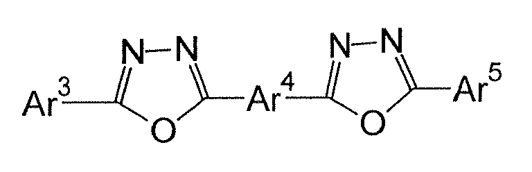

Examples of the aryl group include a phenyl group, a biphenyl group, an anthranil group, a perilenyl group and a pyrenyl group. Further, examples of the arylene group include a phenylene group, a naphthylene group, a biphenylene group, an anthranylene group, a perilenylene group, a pyrenylene group, etc. Furthermore, examples of the substituent include an alkyl group having 1 to 10 carbon atoms, an alkoxy group or a cyano group each having 1 to 10 carbon atoms respectively, etc. With regard to the electron transfer compound, those compounds having a thin film forming capability are preferable. - Specific examples of the electron transfer compounds are shown below:

A nitrogen-containing heterocyclic derivative represented by a following general formula (A) or a following general formula (B):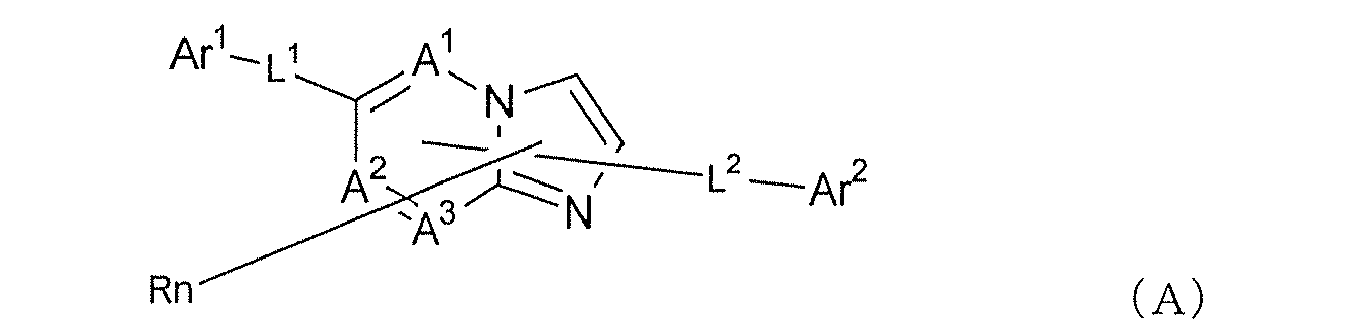
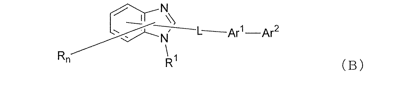
- In the general formulae (A) and (B), A1 to A3 each independently represents nitrogen atom or carbon atom.
Ar1 represents a substituted or unsubstituted aryl group having 6 to 60 ring carbon atoms, or a substituted or unsubstituted hetero aryl group having 3 to 60 ring carbon atoms, Ar2 represents a hydrogen atom, a substituted or unsubstituted aryl group having 6 to 60 ring carbon atoms, or a substituted or unsubstituted hetero aryl group having 3 to 60 ring carbon atoms, a substituted or unsubstituted alkyl group having 1 to 20 carbon atoms, or a substituted or unsubstituted alkoxy group having 1 to 20 carbon atoms, or a bivalent group of these; Either Ar1 or Ar2 is, however, a substituted or unsubstituted condensed ring group having 10 to 60 ring carbon atoms or a substituted or unsubstituted monohetero condensed ring group having 3 to 60 ring carbon atoms.
L1, L2 and L each independently represents a single bond, a substituted or unsubstituted arylene group having 6 to 60 ring carbon atoms, a substituted or unsubstituted hetero arylene group having 3 to 60 ring carbon atoms, or a substituted or unsubstituted fluorene group.
R represents hydrogen, a substituted or unsubstituted aryl group having 6 to 60 ring carbon atoms, or a substituted or unsubstituted hetero aryl group having 3 to 60 ring carbon atoms, a substituted or unsubstituted alkyl group having 1 to 20 carbon atoms, or a substituted or unsubstituted alkoxy group having 1 to 20 carbon atoms. n represents an integer of from 0 to 5, a plural number of R, if any, may be either the same with or different from each other when n is 2. Further, a plural number of R, if any, when these are adjacent to each other, may be bonded each other to form a carbocyclic aliphatic ring or a carbocyclic aromatic ring. - A nitrogen-containing heterocyclic derivative represented by a following general formula (C):
HAr-L-Ar1-Ar2 (C),
In the general formula (C), HAr represents a nitrogen-containing heterocyclic derivative and further may have a substituent, having 3 to 40 of carbon atoms, L represents a single bond, an arylene group and further may have a substituent, having 6 to 60 carbon atoms, a hetero arylene group and further may have a substituent, having 3 to 60 carbon atoms, or a fluorene group and further may have substituent, Ar1 represents a bivalent aromatic hydrocarbon group and further may have a substituent, having 6 to 60 carbon atoms, Ar2 represents an aryl group and further may have a substituent, having 6 to 60 carbon atoms or a hetero aryl group and further may have a substituent, having 3 to 60 carbon atoms, represents a nitrogen-containing heterocyclic derivative. - A silacyclopentadiene derivative represented by a following general formula (D):

- In the general formula (D), X and Y each independently represents a substituted or unsubstituted hydrocarbon group having 1 to 6 of carbon atoms, an alkoxy group, an alkenyloxy group, an alkynyloxy group, a hydroxyl group, a substituted or unsubstituted aryl group, a substituted or unsubstituted hetero ring, or a structure forming a saturated or unsaturated ring by bonding X and Y, of R1 to R4 each represents independently a hydrogen atom, a halogen atom, a substituted or unsubstituted alkyl group having 1 to 6 carbon atoms, an alkoxy group, an aryloxy group, a perfuluoroalkyl group, a perfuluoroalkoxy group, an amino group, an alkylcarbonyl group, an arylcarbonyl group, an alkoxycarbonyl group, an aryloxycarbonyl group, an azo group, an alkylcarbonyloxy group, an arylcarbonyloxy group, an alkoxycarbonyloxy group, an aryloxycarbonyl group, a sulfunyl group, a sulfonyl group, a silyl group, a carbamoyl group, an aryl group, a heterocyclic group, an alkenyl group, a nitro group, a formyl group, a nitroso group, a formyloxy group, an isocyano group, a cyanate group, a thiosyanate group, an isothiosyanate group or a cyano group, or a substituted or unsubstituted condensed ring structure when these are adjacent to each other.
- A borane derivative represented by a following general formula (E):
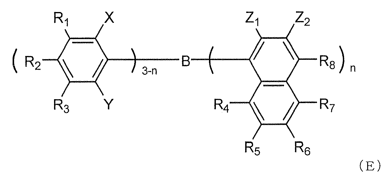
- In the general formula (E), R1 to R8 and Z2 each independently represents a hydrogen atom, a saturated or unsaturated hydrocarbon, an aromatic group, an heterocyclic group, a substituted amino group, a substituted boryl group, an alkoxy group or an aryloxy group, each of X, Y and Z1 represents independently a saturated or unsaturated hydrocarbon, an aromatic group, an heterocyclic group, a substituted amino group, an alkoxy group or an aryloxy group, and substitutes of Z1 and Z2 may bond each other to form a condesed ring, n represents an integer of 1 to 3, Z1 may be different from each other when n is 2 or more; any compound, however, of which n is 1, X, Y and R2 are methyl groups, and R8 is a hydrogen atom or a substituted boryl group, or, of which n is 3 and Z1 is a methyl group, is excluded.
-

- In the general formula (F), Q1 and Q2 each independently represents a ligand shown by the general formula (G), L represents a ligand shown by a halogen atom, a substituted or unsubstituted alkyl group, a substituted or unsubstituted cycloalkyl group, a substituted or unsubstituted aryl group, heterocyclic group, - OR1 (R1 represents a hydrogen atom, a substituted or unsubstituted alkyl group, a substituted or unsubstituted cycloalkyl group, a substituted or unsubstituted aryl group, or a substituted or unsubstituted heterocyclic group or -O-Ga-Q3(Q4) (Q3 and Q4 are the same with Q1 and Q2).
-

- The metal complex shows a strong property as a n-type impurity semiconductor so that a capability of electron injection is significant. In addition, affinity between the metal complex formed and the ligand is strong so that fluorescent quantum efficiency for a light emitting material is increased.
The specific examples of a substituent for A1 and A2 forming a ligand of the general formula (G) include a halogen atom of halogen, bromine and iodine, a substituted or unsubstituted alkyl group such as a methyl group, a ethyl group, a propyl group, a butyl group, a sec-butyl group, a tert-butyl group, a pentyl group, a hexyl group, a heptyl group, an octyl group, a stearyl group and trichloromethyl group, a substituted or unsubstituted aryl group such as a phenyl group, a naphtyl group, a 3-methynaphtyl group, a 3-methoxynaphtyl group, a 3-fluorophenyl group, a 3-trichloromethylphenyl group, a 3-trifluoromethylphenyl group, and a 3-nitrophenyl group, a substituted or unsubstituted alkoxy group such as a methoxy group, a n-butoxy group, a tert-butoxy group, a trichloromethoxy group, a trifluoroethoxy group, a pentafluoroporopoxy group, a 2,2,3,3-tetra fluoroporopoxy group, a 1,1,1,3,3,3-hexafluoro-2-propoxy group, a 6-(perfluoroethyl)hexyloxy group, a substituted or unsubstituted aryloxy group such as a phenoxy group, a p-nitrophenoxy group, a p-tert-butylphenoxy group, a 3-fluorophenoxy group, a pentafluorophenoxy group, and a 3-trifluoromethylphenoxy group, a substituted or unsubstituted alkylthio group such as a methylthio group, an ethylthio group, a tert-butykthio group, a hexylthio group, an octylthio group and a trifluromethylthio group, a substituted or unsubstituted arylthio group such as a phenylthio group, a p-nitrophenylthio group, a p-tert-butylphenylthio group, a 3-fluorophenylthio group, pentafluorophenylthio group and 3-trifluoromethylphenylthio group, a cyano group, a nitro group, an amino group, a mono or di substituted amino group such as a methyamino group, a dimethylamino group, a ethylamino group, a diethylamino group, a dipropylamino group, a dibutylamino group and a diphenylamino group, an acylamino group such as a bis(acetoxymethyl)amino group, a bis(acetoxyethyl) amino group, a bis(acetoxypropyl)amino group and bis(acetoxybutyl)amino group, a hydroxy group, a siloxy group, an acyl group, a carbamoyl group such as a methylcarbamoyl group, dimethylcarbamoyl group, an ethylcarbamoyl group, a diethylcarbamoyl group, a propylcarbamoyl group, a butylcarbamoyl group and phenylcarbamoyl group, a carboxylic acid group, a sulfonic acid group, an imido group, a cycloalkyl group such as a cyclopentane group and a cyclohexyl group, an aryl group such as a phenyl group, a naphthyl group, a biphenyl group, an anthranyl group, a phenanthryl group, a fluorenyl group and a pyrenyl group, and a heterocyclic group such as a pyridinyl group, a pyrazinyl group, a pyrimidyl group, a pyridazinyl group, a triazinyl group, an indolinyl group, a quinolinyl group, an acridinyl group, a pyrrolidyl group, a dioxanyl group, a morpholizinyl group, a piperazinyl group, a triatinyl group, a carbazolyl group, a furanyl group, a thiophenyl group, an oxazolyl group, an oxadiazolyl group, a benzoxazolyl group, a thiazolyl group, a thiadiazolyl group, a benzothiazolyl group, a triazolyl group, an imidazolyl group, a benzoimidazolyl group and a pranyl group. In addition, the above substituent may bond each other to further form a six-member aryl ring or a hetero-ring. - In the present invention, it is preferable that a reductive dopant is added in either the electron transporting zone or an interfacial zone between the cathode and the organic layer. The reductive dopant used in the present invention is defined as a substance which reduces the electron transporting compound. Examples of the reductive dopant include at least one compound selected from alkali metals, alkali metallic complexes, alkali metal compounds, alkaline earth metals, alkaline earth metallic complexes, alkaline earth metal compounds, rare earth metals, rare earth metallic complexes and rare earth metal compounds.
Examples of the preferable reductive dopant include at least one alkali metal selected from a group consisting of Li (the work function: 2.93 ev), Na (the work function: 2.36 eV), K (the work function: 2.28 eV), Rb (the work function: 2.16 eV) and Cs (the work function: 1.95 eV) or at least one alkaline earth metals selected from a group consisting of Ca (the work function: 2.9eV), Sr (the work function: 2.0 to 2.5 eV) and Ba (the work function: 2.52eV); whose work function of 2.9 eV or smaller is particularly preferable. Among the above, the preferable reductive dopant include at least one alkali metal selected from a group consisting of K, Rb and Cs, the more preferred is Rb or Cs, and the most preferred is Cs. These alkali metals have particularly high ability of reduction so that improvement of an emission luminance and longer lasting of a lifetime of the organic EL device may be realized. In addition, a combination of two or more of alkali metals is also preferable as a reductive dopant having 2.9 eV or less of the work function. In particular, a combination of Cs, for example with Na, Cs, K or Rb, or Na and K is preferable. By combing and containing Cs therein, the reduction ability can be demonstrated effectively, and improvement of an emission luminance and longer lasting of a lifetime of the organic EL device may be realized by adding it into an electron injecting zone. - In the organic EL device of the present invention, an electron injecting layer formed with an insulating material or a semiconductor may be further sandwiched between the cathode and the organic thin film layer. The electron injecting layer effectively prevents leak in the electric current and improves the electron injecting capability. It is preferable that at least one metal compound selected from the group consisting of alkali metal chalcogenides, alkaline earth metal chalcogenides, alkali metal halides and alkaline earth metal halides is used as the insulating material.It is preferable that the electron injecting layer is constituted with the above alkali metal chalcogenide since the electron injecting property can be improved. Preferable examples of the alkali metal chalcogenide include Li2O, LiO, Na2S, Na2Se and NaO. Preferable examples of the alkaline earth metal chalcogenide include CaO, BaO, SrO, BeO, BaS and CaSe. Preferable examples of the alkali metal halide include LiF, NaF, KF, LiCl, KCl and NaCl. Preferable examples of the alkaline earth metal halide include fluorides such as CaF2, BaF2, SrF2, MgF2 and BeF2 and halides other than the fluorides.
Examples of the semiconductor constituting the electron transporting layer include oxides, nitrides and nitriding oxides containing at least one element selected from Ba, Ca, Sr, Yb, Al, Ga, In, Li, Na, Cd, Mg, Si, Ta, Sb and Zn, which are used singly or in combination of two or more. It is preferable that the inorganic compound constituting the electron transporting layer is in the form of a fine crystalline or amorphous insulating thin film When the electron transporting layer is constituted with the above insulating thin film, a more uniform thin film can be formed and defective pixels such as dark spots can be decreased. Examples of the inorganic compound include the alkali metal chalcogenides, the alkaline earth metal chalcogenides, the alkali metal halides and the alkaline earth metal halides which are described above. - As the cathode for the organic EL device of the present invention, an electrode substance such as metal, alloy, electroconductive compound and those mixture having a small work function (4 eV or smaller) is employed. Examples of the electrode substance include potassium, sodium- potassium alloy, magnesium, lithium, magnesium-silver alloy, aluminum / aluminum oxide, aluminum-lithium alloy, indium, rare earth metal, etc.
The cathode can be prepared by forming a thin film of the electrode material described above in accordance with a process such as the vapor deposition process and the sputtering process.
When the light emitted from the light emitting layer is observed through the cathode, it is preferable that the cathode has a transmittance of the emitted light greater than 10 %. It is also preferable that the sheet resistivity of the cathode is several hundred Ω/□ or smaller. The thickness of the cathode is, in general, selected in the range of from 10 nm to 1 µm and preferably in the range of from 50 to 200 nm. - In general, an organic EL device tends to form defects in pixels due to leak and short circuit since an electric field is applied to ultra-thin films. To prevent the formation of the defects, a layer of an insulating thin film may be inserted between the pair of electrodes.
Examples of the material employed for the insulating layer include aluminum oxide, lithium fluoride, lithium oxide, cesium fluoride, cesium oxide, magnesium oxide, magnesium fluoride, calcium oxide, calcium fluoride, aluminum nitride, titanium oxide, silicon oxide, germanium oxide, silicon nitride, boron nitride, molybdenum oxide, ruthenium oxide and vanadium oxide. Mixtures and laminates of the above compounds can also be employed. - To produce an organic EL device of the present invention, for example, a cathode, a light emitting layer and, where necessary, a hole injecting layer and an electron injecting layer are formed in accordance with the aforementioned process using the aforementioned materials, and the anode is formed in the last step. An organic EL device may be produced by forming the aforementioned layers in the order reverse to that described above, i.e., an anode being formed in the first step and a cathode in the last step.
An embodiment of the process for producing an organic EL device having a construction in which a cathode, a hole injecting layer, a light emitting layer, an electron injecting layer and an anode are disposed sequentially on a light-transmitting substrate will be described in the following.
On a suitable light-transmitting substrate, a thin film made of a material for the cathode is formed in accordance with the vapor deposition process or the sputtering process so that the thickness of the formed thin film is 1 µm or smaller and preferably in the range of 10 to 200 nm. The formed thin film is employed as the cathode. Then, a hole injecting layer is formed on the cathode. The hole injecting layer can be formed in accordance with the vacuum vapor deposition process, the spin coating process, the casting process or the LB process, as described above. The vacuum vapor deposition process is preferable since a uniform film can be easily obtained and the possibility of formation of pin holes is small.
When the hole injecting layer is formed in accordance with the vacuum vapor deposition process, in general, it is preferable that the conditions in general are suitably selected in the following ranges: temperature of the deposition source: 50 to 450°C; vacuum level: 10-7 to 10-3 Torr; deposition rate: 0.01 to 50 nm/second; temperature of the substrate: -50 to 300°C; and film thickness: 5 nm to 5 µm; although the conditions of the vacuum vapor deposition are different depending on the employed compound (the material for the hole injecting layer) and the crystal structure and the recombination structure of the hole injecting layer to be formed. - Subsequently, the light-emitting layer is formed on the hole-injecting layer formed above. Also the formation of the light emitting layer can be made by forming the light emitting material according to the present invention into a thin film in accordance with the vacuum vapor deposition process, the sputtering process, the spin coating process or the casting process. The vacuum vapor deposition process is preferable because a uniform film can be easily obtained and the possibility of formation of pinholes is small. When the light-emitting layer is formed in accordance with the vacuum vapor deposition process, in general, the conditions of the vacuum vapor deposition process can be selected in the same ranges as those described for the vacuum vapor deposition of the hole-injecting layer although the conditions are different depending on the used compound. It is preferable that the thickness is in the range of from 10 to 40 nm.
- Next, the electron-injecting layer is formed on the light-emitting layer formed above. Similarly to the hole injecting layer and the light-emitting layer, it is preferable that the electron-injecting layer is formed in accordance with the vacuum vapor deposition process since a uniform film must be obtained. The conditions of the vacuum vapor deposition can be selected in the same ranges as those for the hole injecting layer and the light-emitting layer.
In the last step, the anode is formed on the electron injecting layer, and an organic EL device can be fabricated. The anode is made of a metal and can be formed in accordance with the vacuum vapor deposition process or the sputtering process.
It is preferable that the vacuum vapor deposition process is employed in order to prevent the lower organic layers from damages during the formation of the film. In the above production of the organic EL device, it is preferable that the above layers from the anode to the cathode are formed successively while the production system is kept in a vacuum after being evacuated. - The process for forming the layers in the organic EL device of the present invention is not particularly limited. A conventional process such as the vacuum vapor deposition process and the spin coating process can be used. The organic thin film layer comprising the compound having a spiro bond represented by the foregoing general formula (1) used in the organic EL device of the present invention can be formed in accordance with the vacuum vapor deposition process, the molecular beam epitaxy process (the MBE process) or, using a solution prepared by dissolving the compound into a solvent, in accordance with a conventional coating process such as the dipping process, the spin coating process, the casting process, the bar coating process and the roller coating process.
The thickness of each layer in the organic thin film layer in the organic EL device of the present invention is not particularly limited, therefore, a thickness within the range of several nanometers to 1 µ m is preferable so as to reduce the defects such as pin holes and improve the efficiency.
When a direct voltage is applied on the organic EL device produced in the above manner, when a direct voltage of 5 to 40 V is applied in the condition that the cathode is connected to a positive electrode (+) and the anode is connected to a negative electrode (-), then a light emitting is observed. When the connection is reversed, no electric current is produced and no light is emitted at all. When an alternating voltage is applied on the organic EL device, the uniform light emission is observed only in the condition that the polarity of the cathode is positive and the polarity of the anode is negative. When an alternating voltage is applied on the organic EL device, any type of wave shape can be employed. - This invention will be described in further detail with reference to Examples, which does not limit the scope of this invention
- 7.4 g of 4-(naphthalene-1-yl) phenyl boronic acid prepared by a well known method and 7.0 g of conventional 1-bromopyrene were dissolved in 80 ml of dimethoxyethane (DME). Subsequently, 0.58 g of tetrakistriphenylphosphine palladium and 40 ml of 2M-sodium carbonate aqueous solution were added therein, followed by argon displacement. After heating and refluxing over 8 hours, it was stood to cool and then an organic layer was extracted therefrom by toluene. The organic layer was washed by saturated salt water, followed by drying through anhydrous sodium sulfate, and then the organic solvent was removed by an evaporator. The residue was refined through a silica gel chromatography (a developing solvent: toluene) and then 10.0 g of 1-(4-naphthalene-1-yl-phenyl) pyrene was obtained. (yield: 99 %)
10.0 g of 1-(4-naphthalene-1-yl-phenyl)pyrene obtained was dispersed into 100 ml of dimethyl formaldehyde (DMF), and 5.3 g N-bromosuccinamide (NBS) in DMF solution was dropped therein at room temperature. After stirred over 5 hours, it was left around overnight. After the overnight, 150 ml of water was added to it and the deposited crystal was filtrated, followed by water and ethanol washing of the crystal. The crystal obtained was refined through a silica gel chromatography (a developing solvent: hexane / toluene = 2 / 1) and then 4.5 g of 1-bromo-6-(4-naphthalene-1-yl-phenyl)pyrene (the yield: 38%) and 3.8 g of 1-bromo-8-(4-naphthalene-1-yl-phenyl)pyrene were obtained (the yield: 32%) as the intermediates. - 2.7 g of (4-naphthalene-2-yl)phenyl boronic acid prepared by a well known method and 4.5 g of 1-bromo-6-(4-naphthalene-1-yl-phenyl)pyrene were dissolved in 40 ml of DME. Subsequently, 0.22 g of tetrakistriphenylphosphine palladium and 15 ml of 2M-sodium carbonate aqueous solution were added therein, followed by argon displacement. After heating and refluxing over 9 hours, it was stood to cool and an organic layer was extracted therefrom by toluene. The organic layer was washed by saturated salt water, followed by drying through anhydrous sodium sulfate, and then the organic solvent was removed by an evaporator. The residue was refined through a silica gel chromatography (a developing solvent: hexane / toluene = 1 /1) and then 3.1 g of the objective compound (AN-2) was obtained.
The measurement result of the compound by FD-MS (Field Desorption Mass Spectrometry analysis) showed m/z=606 to C48H30 = 606, therefore the objective compound (AN-2) was confirmed (the yield: 54%). - 2.3 g of 3-(naphthalene-2-yl) phenyl boronic acid prepared by a well known method and 3.8 g of 1-bromo-8-(4-napbthalene-1-yl-phenyl) pyrene were dissolved in 40 ml of DME. Subsequently, 0.19 g of tetrakis(triphenylphosphine)palladium and 13 ml of 2M-sodium carbonate aqueous solution were added therein, followed by argon displacement. After heating and refluxing for 9 hours, it was stood to cool and then an organic layer was extracted therefrom by toluene. The organic layer was washed by saturated salt water, followed by drying through anhydrous sodium sulfate, and then the organic solvent was removed by an evaporator. The residue was refined through a silica gel chromatography (a developing solvent: hexane / toluene = 1 /1) and then 2.7 g of the objective compound (AN-7) was obtained.
The measurement result of the compound by FD-MS showed m/z=606 to C48H30 = 606, therefore the objective compound (AN-7) was confirmed (the yield: 58%). - 1-naphthalene boronic acid in place of 4-(naphthalene-1-yl)phenyl boronic acid was used in Synthesis Example 1 (1), and then 1-bromo-6-(naphthalene-1-yl) pyrene and 1-bromo-8-(naphthalene-1-yl) pyrene were obtained.
- The procedure of Synthesis Example 1 (2) was repeated except that 4.0 g of 1-bromo-6-(naphthalene-1-yl)pyrene and 1.85 g of 2-naphthalene boronic acid in place of 4-(naphthalene-2-yl)phenyl boronic acid and 1-bromo-6-(4-naphthalene-1-yl-phenyl)pyrene were used, and then 2.7 g of the light-yellow crystalline objective compound (AN-3) was obtained.
The measurement result of the compound by FD-MS showed m/z=454 to C36H22 = 454, therefore the objective compound (AN-3) was confirmed. - The procedure of the synthesis example 1 (2) was repeated except that 4.0 g of 1-bromo-8-(naphthalene-1-yl)pyrene obtained in Synthesis Example 3 (1) and 1.85 g of 2-naphthalene boronic acid in place of 4-(naphthalene-2-yl)phenyl boronic acid and 1-bromo-6-(4-naphthalene-1-yl-phenyl)pyrene were used, and then 2.9 g of the light-yellow crystalline objective compound (AN-19) was obtained.
The measurement result of the compound by FD-MS showed m/z=454 to C36H22 = 454, therefore the objective compound (AN-19) was confirmed. - 5.0 g of the compound (AN-3) was dispersed in 50 ml of DMF and 4.0 g of NBS in DMF solution was dropped thereto at room temperature. After 3 days reaction, 100 ml of water was added thereto, and the deposited crystal was filtrated, followed by water and ethanol- washing of the crystal. The crystal obtained was refined through a silica gel chromatography (a developing solvent: hexane / toluene = 2 / 1) and then 4.0 g of 1,6-dibromo-3-(naphthalene-2-yl)-8-(naphthalene-1-yl) pyrene was obtained as the intermediate (the yield: 60%) .
4.0 g of 1,6-dibromo-3-(naphthalene-2-yl)-8-(naphthalene-1-yl)pyrene obtained and 1.9 g of phenyl boronic acid were dissolved in 60 ml of DME. Subsequently, 0.5 g of tetrakistriphenylphosphinepalladium and 20 ml of 2M-sodium carbonate aqueous solution were added therein, followed by argon displacement. After heating and refluxing over 8 hours, it was stood to cool and then the deposited crystal was filtrated. After washing the crystal by water and methanol, it was refined through a silica gel chromatography (a developing solvent: toluene), and then 2.9 g of the light-yellow crystalline objective compound (AN-20) was obtained.
The measurement result of the compound by FD-MS showed m/z=606 to C48H30 = 606, therefore the objective compound (AN-20) was confirmed (the yield: 73%). - 8.0 g of 1,6-dinaphthalene-2-yl-pyrene prepared by a well known method was dispersed into 80 ml of DMF, and 3.2 g of NBS in DMF solution was dropped therein at room temperature. After 3 days reaction, 150 ml of water was added to it and the deposited crystal was filtrated, followed by water and ethanol washing of the crystal. The crystal obtained was refined through a silica gel chromatography (a developing solvent: hexane / toluene = 2 / 1) and then 8.5 g of 3-bromo-1,6-dinaphthalene-2-yl-pyrene was obtained as the intermediate (the yield: 90%) . 8.5 g of 3-bromo-1,6-dinaphthalene-2-yl-pyrene obtained and 2.3 g of phenyl boronic acid were dissolved in 100 ml of DME. Subsequently, 0.55 g of tetrakistriphenylphosphinepalladium and 25 ml of 2M-sodium carbonate aqueous solution were added therein, followed by argon displacement. After heating and refluxing over 8 hours, it was stood to cool, and then the deposited crystal was filtrated. After washing the crystal by water and methanol, it was refined through a silica gel chromatography (a developing solvent: toluene), and then 5.4 g of 1,6-dinaphthalene-2-yl-3-phenylpyrene of the light-yellow crystalline was obtained (the yield: 64%).
5.4 g of 1, 6-dinaphthalene-2-yl-3-phenylpyrene was dispersed into 60 ml of DMF, and 1.9 g NBS in DMF solution was dropped therein at room temperature. After 3 days reaction, 150 ml of water was added to it and the deposited crystal was filtrated, followed by water and ethanol washing of the crystal.
The crystal obtained was refined through a silica gel chromatography (a developing solvent: hexane / toluene =2/1) and then 5.9 g of 1-bromo-3,8-dinaphthalene-2-yl-6-phenylpyrene was obtained as the intermediate (the yield: 95%). - 5.9 g of 1-bromo-3,8-dinaphthalene-2-yl-6-phenylpyrene obtained and 2.3 g of 2-biphenyl boronic acid were dissolved in 80 ml of DME. Subsequently, 0.35 g of tetrakistriphenylphosphinepalladium and 15 ml of 2M-sodium carbonate aqueous solution were added therein, followed by argon displacement. After heating and refluxing over 7 hours, it was stood to cool and then the deposited crystal was filtrated. After washing the crystal by water and methanol, it was refined through a silica gel chromatography (a developing solvent: toluene), and then 4.8 g of the light-yellow crystalline objective compound (AN-21) was obtained.
The measurement result of the compound by FD-MS showed m/z=682 to C54H34 = 682, therefore the objective compound (AN-21) was confirmed (the yield: 73%). - 10 g of 2,7-diiodo-9,9'-dimetyl-9H-fluorene prepared by a well known method and 4.6 g of 1-naphthalene boronic acid were dissolved in 150 ml of toluene. Subsequently, 0.78 g of tetrakistriphenylphosphinepalladium and 35 ml of 2M-sodium carbonate aqueous solution were added therein, followed by argon displacement. After heating and refluxing over 8 hours, it was stood to cool and then an organic layer was extracted therefrom by toluene. The organic layer was washed by saturated salt water, followed by drying through anhydrous sodium sulfate, and then the organic solvent was removed by an evaporator. The residue was refined through a silica gel chromatography (a developing solvent: hexane / toluene = 1 /1) and then 7.1 g of diiodo-9,9'-dimetyl-7-naphthalene-1-yl-9H-fluorene was obtained (the yield: 71%).
7.1 g of diiodo-9,9'-dimetyl-7-naphthalene-1-yl-9H-fluorene obtained and 4.7 g of 1-pyrene boronic acid were dissolved in 100 ml of DME. Subsequently, 0.55 g of tetrakistriphenylphosphinepalladium and 25 ml of 2M-sodium carbonate aqueous solution were added therein, followed by argon displacement. After heating and refluxing over 7 hours, it was stood to cool and then the deposited crystal was filtrated. After washing the crystal by water and methanol, it was refined through a silica gel chromatography (a developing solvent: toluene), and then 5.7 g of the light-yellow crystalline objective compound (AN-8) was obtained.
The measurement result of the compound by FD-MS showed m/z=520 to C41H28 = 520, therefore the objective compound (AN-8) was confirmed (the yield: 69%). - A glass substrate (manufactured by GEOMATEC Company) of 25 mm×75 mm×1.1 mm thickness having an ITO transparent electrode was cleaned by application of ultrasonic wave in isopropyl alcohol for 5 minutes and then by exposure to ozone generated by ultraviolet light for 30 minutes. The cleaned glass substrate having an ITO transparent electrode line was fixed to a substrate holder of a vacuum deposition apparatus, and on the surface, where the ITO transparent electrode line was fixed, of the substrate, a film (hereinafter referred to as TPD232 film) having film thickness of 60 nm of the following N,N'-bis(N,N'-diphenyl-4-aminophenyl)-N,N-diphenyl-4,4'-diamino-1,1'-biphel was formed so as to cover the transparent electrode. The TPD232 film performs as a hole injecting layer. Subsequently, a layer having layer thickness of 20 nm of the following N,N,N',N'-tetra(4-biphenyl)-diaminobiphenylene was formed (hereinafter referred to as TBDB layer). The layer performs as a hole transporting layer. Subsequently, a film having a film thickness of 40 nm of the aforementioned compound AN-2 was formed as host material by a vapor deposition. Concurrently, as light emitting material, the following amino compound BD1 containing a styryl group was deposited at the ratio by weight between AN-2 and BD 1 of 40: 3 by a vapor deposition. The film performs as a light emitting layer. On the film, a film having a Alq film thickness of 10 nm was formed. The film performs as an electron injecting layer. Further, a film (film thickness: 10 nm) of Alq : Li (the source of lithium: manufactured by SAES GETTERS Company) as an electron injecting layer was formed by binary vapor deposition of Li as a reductive dopant and the following Alq. On the Alq : Li film, Al metal was deposited to form a metal cathode, therefore, an organic EL device was fabricated.
The device was tested by passing electric current, an emission luminance of 615 cd/m2 and a current efficiency of 6.5cd/Awas observed at a voltage of 5.76V and a current density of 10mA/cm2. In addition, when the EL device was continuously tested by passing electric current at an initial luminance of 1,000cd/m2, the results of the half-lifetime are shown in Table 1. -


- Organic EL devices were fabricated similar to Example 1 except that the compounds described in Table 1 were used in place of the compound (AN-2).
The devices obtained were tested by passing electric current similar to the example 1, the results of the half-lifetime measured at an initial luminance of 1,000cd/m2, are shown in Table 1. - Organic EL devices were fabricated similar to the example 1 except that the following compounds an-1 (Comparative Example 1), an-2 (Comparative Example 2) and an-3 (Comparative Example 3) were used in place of the compound (AN-2).
The devices obtained were tested by passing electric current similar to the example 1, the results of the half-lifetime measured at an initial luminance of 1,000cd/m2, were described in Table 1.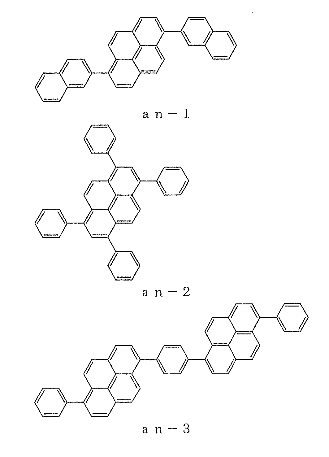
-
Table 1 Material Forming a Light Emitting Layer Driving Voltage (V) Luminance (cd/m2) Current Efficiency (cd/A) Chromaticity Cordinate(x,y) Half-Lifetime (hours) Example 1 AN-2 / BD1 5.76 615 6.15 (0.151,0.174) 2800 Example 2 AN-3/BD1 5.79 611 6.11 (0.151,0.177) 2000 Example 3 AN-9 / BD1 5.64 645 6.45 (0.148,0.198) 1700 Example 4 AN-8/BD1 5.86 616 6.16 (0.147,0.183) 1500 Comparative Example 1 an-1/BD1 6.85 531 5.31 (0.170,0236) 490 Comparative Example 2 an-2/BD1 6.89 550 5.50 (0.199,0.230) 800 Comparative Example 3 an-3/BD1 6.89 558 5.58 (0.159,0229) 700 - As aforementioned in detail, an organic EL device employing a compound having an asymmetric pyrene derivative of the present invention exhibits a great efficiency of light emission and has a long lifetime.
Therefore, they are highly applicable as the organic EL devices supposed to be used continuously for long years.
Claims (17)
- An asymmetric pyrene derivative represented by a following general formula (1):

L and L' each represents a substituted or unsubstituted phenylene group, a substituted or unsubstituted naphthalenylene group, a substituted or unsubstituted fluorenylene group or a substituted or unsubstituted dibenzosilolylene group;
m represents an integer of 0 to 2, n represents an integer of 1 to 4, s represents an integer of 0 to 2 and t represents an integer of 0 to 4; and
L or Ar bonds to any one of 1 to 5 positions of the pyrene, and also L' or Ar' bonds to any one of 6 to 10 thereof;
however, when n + t is an even number, Ar, Ar', L and L' satisfy a following requirement (1) or requirement (2):(1) Ar ≠ Ar' and/or L ≠ L' (wherein ≠ means that each group has a different structure),(2) when Ar = Ar' and L = L',(2-1) m ≠ s and/or n ≠ t, or(2-2) when m = s and n = t;(2-2-1) both L and L' or pyrene bond respectively to a different position of Ar and Ar' or (2-2-2) both L and L' or pyrene bond respectively to the same position of Ar and Ar' excluding a case where both L and L' or both Ar and Ar' bond respectively to 1 and 6, or 2 and 7 positions thereof. - The asymmetric pyrene derivative according to Claim 1, wherein Ar ≠ Ar' in the general formula (1).
- The asymmetric pyrene derivative according to Claim 1, wherein L ≠ L' in the general formula (1).
- The asymmetric pyrene derivative according to Claim 1, wherein Ar = Ar' and L ≠ L', and m ≠ s and/or n ≠ t in the general formula (1).
- The asymmetric pyrene derivative according to Claim 1, wherein m = s and n = t, and wherein the following requirement (2-2-1) or (2-2-2) is satisfied in the general formula (1);(2-2-1) both L and L' or pyrene each bonds respectively to different positions of Ar and Ar',(2-2-2) both L and L' or pyrene each bonds respectively to the same positions of Ar and Ar', excluding a case where both L and L' or both Ar and Ar' bond to 1 and 6 positions thereof, or 2 and 5 positions thereof.
- An asymmetric pyrene derivative represented by a following general formula (2):

L and L' each represents a substituted or unsubstituted pheylene group, a substituted or unsubstituted naphthalenylene group, a substituted or unsubstituted fluorenylene group or a substituted or unsubstituted dibenzosilolylene group;
m represents an integer of 0 to 2, s represents an integer of 0 to 2 and t represents an integer of 0 to 4; and
L' or Ar' bonds to any one of 2 to 10 positions of pyrene;
however, when t is an odd number, Ar, Ar', L and L' satisfy the following requirement (1') or a requirement (2'):(1') Ar ≠ Ar' and/or L ≠ L' (wherein ≠ means that each group has a different structure),(2') when Ar = Ar' and L = L',(2-1') m ≠ s and/or n ≠ t, or(2-2') when m = s and n = t,(2-2-1') both L and L' or pyrene each bonds respectively to different positions of Ar and Ar', or(2-2-2') both L and L' or pyrene each bonds to the same positions of Ar and Ar', excluding a case where L' or Ar' bonds to 6 position thereof. - The asymmetric pyrene derivative according to Claim 6, wherein Ar ≠ Ar' in the general formula (2).
- The asymmetric pyrene derivative according to Claim 6, wherein L ≠ L' in the general formula (2).
- The asymmetric pyrene derivative according to Claim 6, wherein Ar = Ar' and L ≠ L', and m ≠ s and/or n ≠ t in the general formula (2).
- The asymmetric pyrene derivative according to Claim 6, wherein, m = s and n = t, and wherein the following requirement (2-2-1') or (2-2-2') is satisfied in the general formula (1):(2-2-1') both L and L' or pyrene each bonds respectively to different positions of Ar and Ar',(2-2-2') both L and L' or pyrene each bonds respectively to the same positions of Ar and Ar', excluding a case where L' or Ar' bonds to 6 position thereof.
- An asymmetric pyrene derivative represented by a following general formula (3):
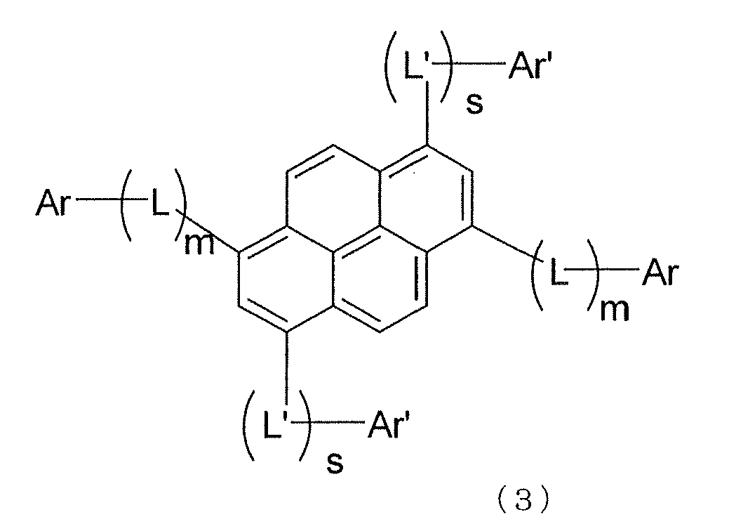
L and L' each represents a substituted or unsubstituted phenylene group, a substituted or unsubstituted naphthalenylene group, a substituted or unsubstituted fluorenylene group or a substituted or unsubstituted dibenzosilolylene group;
m represents an integer of 0 to 2 and s represents an integer of 0 to 2. - The asymmetric pyrene derivative according to any one of Claims 1 to 11, which is a light emitting material for an organic electroluminescence device.
- The asymmetric pyrene derivative according to any one of Claims 1 to 11, which is a host material for an organic electroluminescence device.
- An organic electroluminescence device which comprises at least one organic thin film layer including a light emitting layer sandwiched between a pair of electrode consisting of an anode and a cathode, wherein the organic thin film layer comprises at least one kind selected from asymmetric pyrene derivatives according to any one of Claims 1 to 10 singly or as its mixture component.
- The organic electroluminescence device according to Claim 14, wherein the light emitting layer comprises any one of the organic pyrene derivatives according to Claims 1 to 11 as a host material.
- The organic electroluminescence device according to Claim 14, wherein the light emitting layer further comprises an arylamine compound.
- The organic electroluminescence device according to Claim 14, wherein the light emitting layer further comprises a styrylamine compound.
Applications Claiming Priority (2)
| Application Number | Priority Date | Filing Date | Title |
|---|---|---|---|
| JP2004157571 | 2004-05-27 | ||
| PCT/JP2005/008494 WO2005115950A1 (en) | 2004-05-27 | 2005-05-10 | Asymmetric pyrene derivative and organic electroluminescent device using same |
Publications (3)
| Publication Number | Publication Date |
|---|---|
| EP1749809A1 true EP1749809A1 (en) | 2007-02-07 |
| EP1749809A8 EP1749809A8 (en) | 2007-04-25 |
| EP1749809A4 EP1749809A4 (en) | 2008-07-02 |
Family
ID=35450798
Family Applications (1)
| Application Number | Title | Priority Date | Filing Date |
|---|---|---|---|
| EP05739101A Withdrawn EP1749809A4 (en) | 2004-05-27 | 2005-05-10 | Asymmetric pyrene derivative and organic electroluminescent device using same |
Country Status (7)
| Country | Link |
|---|---|
| US (2) | US7763761B2 (en) |
| EP (1) | EP1749809A4 (en) |
| JP (2) | JP4705914B2 (en) |
| KR (1) | KR20070029717A (en) |
| CN (1) | CN1960957A (en) |
| TW (1) | TW200607849A (en) |
| WO (1) | WO2005115950A1 (en) |
Cited By (38)
| Publication number | Priority date | Publication date | Assignee | Title |
|---|---|---|---|---|
| EP1746080A1 (en) * | 2004-05-12 | 2007-01-24 | Idemitsu Kosan Co., Ltd. | 1,6-substituted 3,8-dihalogenopyrene and process for producing the same |
| CN102473848A (en) * | 2009-12-21 | 2012-05-23 | 出光兴产株式会社 | Organic electroluminescent element using pyrene derivative |
| EP2518038A1 (en) * | 2009-12-21 | 2012-10-31 | Idemitsu Kosan Co., Ltd. | Pyrene derivative and organic electroluminescent element using the same |
| WO2014067614A1 (en) | 2012-10-31 | 2014-05-08 | Merck Patent Gmbh | Electronic device |
| WO2014106524A2 (en) | 2013-01-03 | 2014-07-10 | Merck Patent Gmbh | Materials for electronic devices |
| WO2014106523A1 (en) | 2013-01-03 | 2014-07-10 | Merck Patent Gmbh | Electronic device |
| WO2016119992A1 (en) | 2015-01-30 | 2016-08-04 | Merck Patent Gmbh | Materials for electronic devices |
| WO2017133829A1 (en) | 2016-02-05 | 2017-08-10 | Merck Patent Gmbh | Materials for electronic devices |
| WO2018069167A1 (en) | 2016-10-10 | 2018-04-19 | Merck Patent Gmbh | Electronic device |
| DE102017008794A1 (en) | 2016-10-17 | 2018-04-19 | Merck Patent Gmbh | Materials for use in electronic devices |
| WO2018083053A1 (en) | 2016-11-02 | 2018-05-11 | Merck Patent Gmbh | Materials for electronic devices |
| WO2018087020A1 (en) | 2016-11-08 | 2018-05-17 | Merck Patent Gmbh | Compounds for electronic devices |
| WO2018095839A1 (en) | 2016-11-22 | 2018-05-31 | Merck Patent Gmbh | Bridged triarylamines for electronic devices |
| WO2018114882A1 (en) | 2016-12-22 | 2018-06-28 | Merck Patent Gmbh | Materials for electronic devices |
| WO2018141706A1 (en) | 2017-02-02 | 2018-08-09 | Merck Patent Gmbh | Materials for electronic devices |
| WO2018157981A1 (en) | 2017-03-02 | 2018-09-07 | Merck Patent Gmbh | Materials for organic electronic devices |
| EP3378857A1 (en) | 2012-11-12 | 2018-09-26 | Merck Patent GmbH | Materials for electronic devices |
| WO2018197447A1 (en) | 2017-04-25 | 2018-11-01 | Merck Patent Gmbh | Compounds for electronic devices |
| WO2018234346A1 (en) | 2017-06-23 | 2018-12-27 | Merck Patent Gmbh | Materials for organic electroluminescent devices |
| WO2018234220A1 (en) | 2017-06-21 | 2018-12-27 | Merck Patent Gmbh | Materials for electronic devices |
| WO2019002190A1 (en) | 2017-06-28 | 2019-01-03 | Merck Patent Gmbh | Materials for electronic devices |
| WO2019002198A1 (en) | 2017-06-26 | 2019-01-03 | Merck Patent Gmbh | Homogeneous mixtures |
| WO2019020654A1 (en) | 2017-07-28 | 2019-01-31 | Merck Patent Gmbh | Spirobifluorene derivatives for use in electronic devices |
| WO2019048443A1 (en) | 2017-09-08 | 2019-03-14 | Merck Patent Gmbh | Materials for electronic devices |
| WO2019101719A1 (en) | 2017-11-23 | 2019-05-31 | Merck Patent Gmbh | Materials for electronic devices |
| WO2019115577A1 (en) | 2017-12-15 | 2019-06-20 | Merck Patent Gmbh | Substituted aromatic amines for use in organic electroluminescent devices |
| WO2019121483A1 (en) | 2017-12-20 | 2019-06-27 | Merck Patent Gmbh | Heteroaromatic compounds |
| WO2019175149A1 (en) | 2018-03-16 | 2019-09-19 | Merck Patent Gmbh | Materials for organic electroluminescent devices |
| WO2020178230A1 (en) | 2019-03-04 | 2020-09-10 | Merck Patent Gmbh | Ligands for nano-sized materials |
| WO2023052275A1 (en) | 2021-09-28 | 2023-04-06 | Merck Patent Gmbh | Materials for electronic devices |
| WO2023052272A1 (en) | 2021-09-28 | 2023-04-06 | Merck Patent Gmbh | Materials for electronic devices |
| WO2023052314A1 (en) | 2021-09-28 | 2023-04-06 | Merck Patent Gmbh | Materials for electronic devices |
| WO2023052313A1 (en) | 2021-09-28 | 2023-04-06 | Merck Patent Gmbh | Materials for electronic devices |
| WO2023094412A1 (en) | 2021-11-25 | 2023-06-01 | Merck Patent Gmbh | Materials for electronic devices |
| WO2023117837A1 (en) | 2021-12-21 | 2023-06-29 | Merck Patent Gmbh | Process for preparing deuterated organic compounds |
| WO2023152346A1 (en) | 2022-02-14 | 2023-08-17 | Merck Patent Gmbh | Materials for electronic devices |
| WO2023222559A1 (en) | 2022-05-18 | 2023-11-23 | Merck Patent Gmbh | Process for preparing deuterated organic compounds |
| WO2024013004A1 (en) | 2022-07-11 | 2024-01-18 | Merck Patent Gmbh | Materials for electronic devices |
Families Citing this family (54)
| Publication number | Priority date | Publication date | Assignee | Title |
|---|---|---|---|---|
| JP4705914B2 (en) * | 2004-05-27 | 2011-06-22 | 出光興産株式会社 | Asymmetric pyrene derivative and organic electroluminescence device using the same |
| WO2006103916A1 (en) * | 2005-03-25 | 2006-10-05 | Idemitsu Kosan Co., Ltd. | Organic electroluminescent device |
| JP2007015961A (en) * | 2005-07-06 | 2007-01-25 | Idemitsu Kosan Co Ltd | Pyrene derivative and organic electroluminescent element using the same |
| JPWO2007099802A1 (en) * | 2006-02-23 | 2009-07-16 | 出光興産株式会社 | Red organic electroluminescence device |
| WO2007099872A1 (en) * | 2006-02-23 | 2007-09-07 | Idemitsu Kosan Co., Ltd. | Organic electroluminescent device |
| US9214636B2 (en) * | 2006-02-28 | 2015-12-15 | Idemitsu Kosan Co., Ltd. | Organic electroluminescence device |
| JP5093879B2 (en) * | 2006-03-20 | 2012-12-12 | 国立大学法人京都大学 | Pyrene-based organic compounds, transistor materials, and light-emitting transistor elements |
| JP4273132B2 (en) * | 2006-04-03 | 2009-06-03 | セイコーエプソン株式会社 | Manufacturing method of organic light emitting device |
| JP5091854B2 (en) | 2006-04-18 | 2012-12-05 | 出光興産株式会社 | Aromatic amine derivative and organic electroluminescence device using the same |
| KR101362032B1 (en) * | 2006-11-15 | 2014-02-11 | 이데미쓰 고산 가부시키가이샤 | Fluoranthene compound, organic electroluminescent device using the fluoranthene compound, and organic electroluminescent material-containing solution |
| JP4994802B2 (en) * | 2006-11-17 | 2012-08-08 | キヤノン株式会社 | Pyrene compounds and organic light emitting devices |
| JP5428147B2 (en) * | 2006-12-07 | 2014-02-26 | 三菱化学株式会社 | Organic phosphor material |
| US8257836B2 (en) | 2006-12-29 | 2012-09-04 | E I Du Pont De Nemours And Company | Di-substituted pyrenes for luminescent applications |
| CN101641390B (en) * | 2007-04-02 | 2013-05-01 | 第一毛织株式会社 | Hardmask composition having antireflective property and method of patterning materials using the same |
| JPWO2008136522A1 (en) * | 2007-05-08 | 2010-07-29 | 出光興産株式会社 | Diaminopyrene derivative and organic EL device using the same |
| WO2008149968A1 (en) * | 2007-06-07 | 2008-12-11 | Idemitsu Kosan Co., Ltd. | Aromatic amine derivative and organic electroluminescent device |
| WO2009066600A1 (en) * | 2007-11-19 | 2009-05-28 | Idemitsu Kosan Co., Ltd. | Monobenzochrysene derivative, organic electroluminescent device material containing the same, and organic electroluminescent device using the organic electroluminescent device material |
| JPWO2009066666A1 (en) * | 2007-11-20 | 2011-04-07 | 出光興産株式会社 | Polymer compound and organic electroluminescence device using the same |
| US8192848B2 (en) | 2008-01-11 | 2012-06-05 | E I Du Pont De Nemours And Company | Substituted pyrenes and associated production methods for luminescent applications |
| KR100901887B1 (en) * | 2008-03-14 | 2009-06-09 | (주)그라쎌 | Novel organic electroluminescent compounds and organic electroluminescent device using the same |
| JP5424681B2 (en) * | 2008-04-01 | 2014-02-26 | キヤノン株式会社 | Organic light emitting device |
| WO2010001817A1 (en) | 2008-07-01 | 2010-01-07 | 東レ株式会社 | Light-emitting element |
| JP5396397B2 (en) | 2008-11-10 | 2014-01-22 | 出光興産株式会社 | Aromatic amine derivative and organic electroluminescence device using the same |
| JP2010138090A (en) * | 2008-12-10 | 2010-06-24 | Canon Inc | New pyrene compound |
| KR101494789B1 (en) * | 2008-12-30 | 2015-02-24 | 엘지디스플레이 주식회사 | Organci emitting material and organic light emitting device using thereof |
| US8759818B2 (en) | 2009-02-27 | 2014-06-24 | E I Du Pont De Nemours And Company | Deuterated compounds for electronic applications |
| KR101582707B1 (en) | 2009-04-03 | 2016-01-05 | 이 아이 듀폰 디 네모아 앤드 캄파니 | Electroactive materials |
| JP5627209B2 (en) * | 2009-09-14 | 2014-11-19 | キヤノン株式会社 | Novel pyrene compound and organic EL device having the same |
| TW201111326A (en) * | 2009-09-29 | 2011-04-01 | Du Pont | Deuterated compounds for luminescent applications |
| CN102596950A (en) | 2009-10-29 | 2012-07-18 | E.I.内穆尔杜邦公司 | Deuterated compounds for electronic applications |
| JP2013512985A (en) * | 2009-12-03 | 2013-04-18 | コリア リサーチ インスティテュート オブ ケミカル テクノロジー | Conductive polymer introduced with pyrene compound and organic solar cell using the same |
| KR101182447B1 (en) * | 2010-06-16 | 2012-09-12 | 삼성디스플레이 주식회사 | Organic light emitting device and manufacturing method thereof |
| KR101334204B1 (en) | 2010-10-27 | 2013-11-28 | (주)위델소재 | A New Pyrene Compounds, Method of Producing the Same and Organic Electroluminescent Device Comprising the Same |
| EP2655547A1 (en) | 2010-12-20 | 2013-10-30 | E.I. Du Pont De Nemours And Company | Compositions for electronic applications |
| JP2013253023A (en) * | 2012-06-05 | 2013-12-19 | Canon Inc | New benzopyrene compound and organic light-emitting element having the same |
| KR101918712B1 (en) | 2012-08-02 | 2018-11-15 | 삼성디스플레이 주식회사 | Organic light emitting diode device |
| JP6305068B2 (en) | 2013-04-30 | 2018-04-04 | キヤノン株式会社 | Organic light emitting device |
| WO2016133058A1 (en) * | 2015-02-18 | 2016-08-25 | Tdk株式会社 | Electroluminescent element |
| US9954187B2 (en) | 2016-04-08 | 2018-04-24 | Idemitsu Kosan Co., Ltd. | Compound, organic electroluminescence device and electronic device |
| JP6830827B2 (en) * | 2017-02-03 | 2021-02-17 | 出光興産株式会社 | Materials for organic electroluminescence devices, electronic devices and organic electroluminescence devices |
| KR102563713B1 (en) | 2017-04-26 | 2023-08-07 | 오티아이 루미오닉스 인크. | Methods of patterning the coating of a surface and apparatus comprising the patterned coating |
| JP7340171B2 (en) * | 2018-01-24 | 2023-09-07 | 学校法人関西学院 | organic electroluminescent device |
| US11751415B2 (en) | 2018-02-02 | 2023-09-05 | Oti Lumionics Inc. | Materials for forming a nucleation-inhibiting coating and devices incorporating same |
| JP7325731B2 (en) | 2018-08-23 | 2023-08-15 | 国立大学法人九州大学 | organic electroluminescence element |
| KR20210149058A (en) | 2019-03-07 | 2021-12-08 | 오티아이 루미오닉스 인크. | Material for forming nucleation inhibiting coating and device comprising same |
| CN114402454A (en) | 2019-09-13 | 2022-04-26 | 出光兴产株式会社 | Organic electroluminescent element and electronic device |
| JPWO2021049662A1 (en) | 2019-09-13 | 2021-03-18 | ||
| WO2021049656A1 (en) | 2019-09-13 | 2021-03-18 | 出光興産株式会社 | Organic electroluminescent element and electronic device |
| JPWO2021049651A1 (en) | 2019-09-13 | 2021-03-18 | ||
| US11094886B2 (en) | 2019-09-13 | 2021-08-17 | Idemitsu Kosan Co., Ltd. | Organic electroluminescent element and electronic device |
| WO2021049660A1 (en) | 2019-09-13 | 2021-03-18 | 出光興産株式会社 | Organic electroluminescent element and electronic device |
| KR20220104237A (en) | 2019-11-26 | 2022-07-26 | 이데미쓰 고산 가부시키가이샤 | Compounds, organic electroluminescent devices and electronic devices |
| JPWO2021162057A1 (en) | 2020-02-14 | 2021-08-19 | ||
| WO2021210304A1 (en) | 2020-04-15 | 2021-10-21 | 出光興産株式会社 | Compound, organic electroluminescent element and electronic device |
Citations (2)
| Publication number | Priority date | Publication date | Assignee | Title |
|---|---|---|---|---|
| US20040076852A1 (en) * | 2002-10-16 | 2004-04-22 | National Tsing Hua University | Aromatic compounds and organic light emitting diodes |
| EP1718124A1 (en) * | 2004-02-19 | 2006-11-02 | Idemitsu Kosan Co., Ltd. | White color organic electroluminescence device |
Family Cites Families (32)
| Publication number | Priority date | Publication date | Assignee | Title |
|---|---|---|---|---|
| JP2897138B2 (en) | 1989-06-30 | 1999-05-31 | 株式会社リコー | EL device |
| JPH03245490A (en) * | 1990-02-23 | 1991-11-01 | Toshiba Corp | Organic membrane luminous element |
| JP3200889B2 (en) | 1991-10-23 | 2001-08-20 | ソニー株式会社 | Image vibration correction device |
| JPH07138561A (en) | 1993-11-17 | 1995-05-30 | Idemitsu Kosan Co Ltd | Organic electroluminescent element |
| JP3506281B2 (en) | 1995-01-26 | 2004-03-15 | 出光興産株式会社 | Organic electroluminescence device |
| JP3724833B2 (en) | 1995-03-06 | 2005-12-07 | 出光興産株式会社 | Organic electroluminescence device |
| JP3712760B2 (en) * | 1995-05-17 | 2005-11-02 | Tdk株式会社 | Organic EL device |
| CA2238689A1 (en) | 1995-11-27 | 1997-06-05 | Idemitsu Kosan Co., Ltd. | Triazine derivatives |
| JP2000273055A (en) * | 1999-03-25 | 2000-10-03 | Idemitsu Kosan Co Ltd | Distyrylarylene derivative and organic electroluminescent element using the same |
| JP5073899B2 (en) * | 1999-09-21 | 2012-11-14 | 出光興産株式会社 | Organic electroluminescence device and organic light emitting medium |
| JP3905265B2 (en) | 1999-10-21 | 2007-04-18 | 富士フイルム株式会社 | Organic electroluminescence device |
| JP3949363B2 (en) * | 1999-10-26 | 2007-07-25 | 富士フイルム株式会社 | Aromatic fused ring compound, light emitting device material, and light emitting device using the same |
| JP2002063988A (en) | 2000-08-22 | 2002-02-28 | Toray Ind Inc | Light emitting element |
| JP3487822B2 (en) | 2000-11-27 | 2004-01-19 | Necパーソナルプロダクツ株式会社 | Apparatus for protecting a moving part of electronic equipment and method of protecting the same |
| JP3870102B2 (en) * | 2001-02-22 | 2007-01-17 | キヤノン株式会社 | Organic light emitting device |
| JP2002250684A (en) * | 2001-02-26 | 2002-09-06 | Shimadzu Corp | Material testing machine |
| JP4593825B2 (en) * | 2001-04-27 | 2010-12-08 | 株式会社豊田中央研究所 | Organic electroluminescence device |
| JP2002334785A (en) * | 2001-05-08 | 2002-11-22 | Fuji Photo Film Co Ltd | Luminescent element |
| JP4566453B2 (en) * | 2001-05-18 | 2010-10-20 | 株式会社豊田中央研究所 | Organic electroluminescence device |
| EP1412450B1 (en) * | 2001-07-11 | 2012-02-29 | FUJIFILM Corporation | Light-emitting device and aromatic compound |
| JP4646494B2 (en) * | 2002-04-11 | 2011-03-09 | 出光興産株式会社 | Novel nitrogen-containing heterocyclic derivative and organic electroluminescence device using the same |
| JP4338367B2 (en) * | 2002-07-11 | 2009-10-07 | 三井化学株式会社 | Compound, organic electroluminescent element material, and organic electroluminescent element |
| JP4025137B2 (en) * | 2002-08-02 | 2007-12-19 | 出光興産株式会社 | Anthracene derivative and organic electroluminescence device using the same |
| JP2004075567A (en) | 2002-08-12 | 2004-03-11 | Idemitsu Kosan Co Ltd | Oligoarylene derivative and organic electroluminescent element using the same |
| TWI284485B (en) | 2002-08-23 | 2007-07-21 | Idemitsu Kosan Co | Organic electroluminescence device and anthracene derivative |
| JP3902993B2 (en) | 2002-08-27 | 2007-04-11 | キヤノン株式会社 | Fluorene compound and organic light emitting device using the same |
| EP1437395B2 (en) * | 2002-12-24 | 2015-08-26 | LG Display Co., Ltd. | Organic electroluminescent device |
| WO2004063159A1 (en) | 2003-01-10 | 2004-07-29 | Idemitsu Kosan Co., Ltd. | Nitrogenous heterocyclic derivative and organic electroluminescent element employing the same |
| US7651788B2 (en) * | 2003-03-05 | 2010-01-26 | Lg Display Co., Ltd. | Organic electroluminescent device |
| JP4351479B2 (en) * | 2003-06-19 | 2009-10-28 | 三井化学株式会社 | Five-membered ring compound and organic electroluminescent device containing the five-membered ring compound |
| US7233019B2 (en) * | 2004-04-26 | 2007-06-19 | E. I. Du Pont De Nemours And Company | Electroluminescent silylated pyrenes, and devices made with such compounds |
| JP4705914B2 (en) * | 2004-05-27 | 2011-06-22 | 出光興産株式会社 | Asymmetric pyrene derivative and organic electroluminescence device using the same |
-
2005
- 2005-05-10 JP JP2006519530A patent/JP4705914B2/en active Active
- 2005-05-10 KR KR1020067024933A patent/KR20070029717A/en not_active Application Discontinuation
- 2005-05-10 CN CNA200580017149XA patent/CN1960957A/en active Pending
- 2005-05-10 WO PCT/JP2005/008494 patent/WO2005115950A1/en not_active Application Discontinuation
- 2005-05-10 EP EP05739101A patent/EP1749809A4/en not_active Withdrawn
- 2005-05-23 TW TW094116768A patent/TW200607849A/en unknown
- 2005-11-21 US US11/282,582 patent/US7763761B2/en active Active
-
2010
- 2010-06-07 US US12/795,216 patent/US8318995B2/en active Active
- 2010-12-14 JP JP2010277867A patent/JP5374486B2/en active Active
Patent Citations (2)
| Publication number | Priority date | Publication date | Assignee | Title |
|---|---|---|---|---|
| US20040076852A1 (en) * | 2002-10-16 | 2004-04-22 | National Tsing Hua University | Aromatic compounds and organic light emitting diodes |
| EP1718124A1 (en) * | 2004-02-19 | 2006-11-02 | Idemitsu Kosan Co., Ltd. | White color organic electroluminescence device |
Non-Patent Citations (1)
| Title |
|---|
| See also references of WO2005115950A1 * |
Cited By (44)
| Publication number | Priority date | Publication date | Assignee | Title |
|---|---|---|---|---|
| EP1746080A4 (en) * | 2004-05-12 | 2007-07-04 | Idemitsu Kosan Co | 1,6-substituted 3,8-dihalogenopyrene and process for producing the same |
| EP1746080A1 (en) * | 2004-05-12 | 2007-01-24 | Idemitsu Kosan Co., Ltd. | 1,6-substituted 3,8-dihalogenopyrene and process for producing the same |
| CN102473848A (en) * | 2009-12-21 | 2012-05-23 | 出光兴产株式会社 | Organic electroluminescent element using pyrene derivative |
| EP2518038A1 (en) * | 2009-12-21 | 2012-10-31 | Idemitsu Kosan Co., Ltd. | Pyrene derivative and organic electroluminescent element using the same |
| EP2518038A4 (en) * | 2009-12-21 | 2013-06-26 | Idemitsu Kosan Co | Pyrene derivative and organic electroluminescent element using the same |
| WO2014067614A1 (en) | 2012-10-31 | 2014-05-08 | Merck Patent Gmbh | Electronic device |
| EP3806176A1 (en) | 2012-10-31 | 2021-04-14 | Merck Patent GmbH | Electronic device |
| EP3378857A1 (en) | 2012-11-12 | 2018-09-26 | Merck Patent GmbH | Materials for electronic devices |
| WO2014106524A2 (en) | 2013-01-03 | 2014-07-10 | Merck Patent Gmbh | Materials for electronic devices |
| WO2014106523A1 (en) | 2013-01-03 | 2014-07-10 | Merck Patent Gmbh | Electronic device |
| WO2016119992A1 (en) | 2015-01-30 | 2016-08-04 | Merck Patent Gmbh | Materials for electronic devices |
| WO2017133829A1 (en) | 2016-02-05 | 2017-08-10 | Merck Patent Gmbh | Materials for electronic devices |
| WO2018069167A1 (en) | 2016-10-10 | 2018-04-19 | Merck Patent Gmbh | Electronic device |
| EP4113643A1 (en) | 2016-10-10 | 2023-01-04 | Merck Patent GmbH | Electronic device |
| EP4255151A2 (en) | 2016-10-10 | 2023-10-04 | Merck Patent GmbH | Spiro[fluorene-9,9'-(thio)xanthene] compounds |
| DE102017008794A1 (en) | 2016-10-17 | 2018-04-19 | Merck Patent Gmbh | Materials for use in electronic devices |
| WO2018083053A1 (en) | 2016-11-02 | 2018-05-11 | Merck Patent Gmbh | Materials for electronic devices |
| WO2018087020A1 (en) | 2016-11-08 | 2018-05-17 | Merck Patent Gmbh | Compounds for electronic devices |
| WO2018095839A1 (en) | 2016-11-22 | 2018-05-31 | Merck Patent Gmbh | Bridged triarylamines for electronic devices |
| WO2018114882A1 (en) | 2016-12-22 | 2018-06-28 | Merck Patent Gmbh | Materials for electronic devices |
| WO2018141706A1 (en) | 2017-02-02 | 2018-08-09 | Merck Patent Gmbh | Materials for electronic devices |
| WO2018157981A1 (en) | 2017-03-02 | 2018-09-07 | Merck Patent Gmbh | Materials for organic electronic devices |
| WO2018197447A1 (en) | 2017-04-25 | 2018-11-01 | Merck Patent Gmbh | Compounds for electronic devices |
| WO2018234220A1 (en) | 2017-06-21 | 2018-12-27 | Merck Patent Gmbh | Materials for electronic devices |
| WO2018234346A1 (en) | 2017-06-23 | 2018-12-27 | Merck Patent Gmbh | Materials for organic electroluminescent devices |
| WO2019002198A1 (en) | 2017-06-26 | 2019-01-03 | Merck Patent Gmbh | Homogeneous mixtures |
| WO2019002190A1 (en) | 2017-06-28 | 2019-01-03 | Merck Patent Gmbh | Materials for electronic devices |
| WO2019020654A1 (en) | 2017-07-28 | 2019-01-31 | Merck Patent Gmbh | Spirobifluorene derivatives for use in electronic devices |
| WO2019048443A1 (en) | 2017-09-08 | 2019-03-14 | Merck Patent Gmbh | Materials for electronic devices |
| WO2019101719A1 (en) | 2017-11-23 | 2019-05-31 | Merck Patent Gmbh | Materials for electronic devices |
| EP4242286A2 (en) | 2017-11-23 | 2023-09-13 | Merck Patent GmbH | Materials for electronic devices |
| WO2019115577A1 (en) | 2017-12-15 | 2019-06-20 | Merck Patent Gmbh | Substituted aromatic amines for use in organic electroluminescent devices |
| WO2019121483A1 (en) | 2017-12-20 | 2019-06-27 | Merck Patent Gmbh | Heteroaromatic compounds |
| WO2019175149A1 (en) | 2018-03-16 | 2019-09-19 | Merck Patent Gmbh | Materials for organic electroluminescent devices |
| WO2020178230A1 (en) | 2019-03-04 | 2020-09-10 | Merck Patent Gmbh | Ligands for nano-sized materials |
| WO2023052314A1 (en) | 2021-09-28 | 2023-04-06 | Merck Patent Gmbh | Materials for electronic devices |
| WO2023052313A1 (en) | 2021-09-28 | 2023-04-06 | Merck Patent Gmbh | Materials for electronic devices |
| WO2023052272A1 (en) | 2021-09-28 | 2023-04-06 | Merck Patent Gmbh | Materials for electronic devices |
| WO2023052275A1 (en) | 2021-09-28 | 2023-04-06 | Merck Patent Gmbh | Materials for electronic devices |
| WO2023094412A1 (en) | 2021-11-25 | 2023-06-01 | Merck Patent Gmbh | Materials for electronic devices |
| WO2023117837A1 (en) | 2021-12-21 | 2023-06-29 | Merck Patent Gmbh | Process for preparing deuterated organic compounds |
| WO2023152346A1 (en) | 2022-02-14 | 2023-08-17 | Merck Patent Gmbh | Materials for electronic devices |
| WO2023222559A1 (en) | 2022-05-18 | 2023-11-23 | Merck Patent Gmbh | Process for preparing deuterated organic compounds |
| WO2024013004A1 (en) | 2022-07-11 | 2024-01-18 | Merck Patent Gmbh | Materials for electronic devices |
Also Published As
| Publication number | Publication date |
|---|---|
| KR20070029717A (en) | 2007-03-14 |
| CN1960957A (en) | 2007-05-09 |
| EP1749809A4 (en) | 2008-07-02 |
| US8318995B2 (en) | 2012-11-27 |
| TW200607849A (en) | 2006-03-01 |
| JP4705914B2 (en) | 2011-06-22 |
| WO2005115950A1 (en) | 2005-12-08 |
| US20100308718A1 (en) | 2010-12-09 |
| EP1749809A8 (en) | 2007-04-25 |
| JPWO2005115950A1 (en) | 2008-03-27 |
| US20060154107A1 (en) | 2006-07-13 |
| JP2011066446A (en) | 2011-03-31 |
| JP5374486B2 (en) | 2013-12-25 |
| US7763761B2 (en) | 2010-07-27 |
Similar Documents
| Publication | Publication Date | Title |
|---|---|---|
| US8318995B2 (en) | Asymmetric pyrene derivative and organic electroluminescence device employing the same | |
| US10205101B2 (en) | Light-emitting material for organic electroluminescent device, organic electroluminescent device using same, and material for organic electroluminescent device | |
| US7504526B2 (en) | Anthracene derivative and organic electroluminescence device employing the same | |
| JP5015459B2 (en) | Asymmetric monoanthracene derivative, material for organic electroluminescence device, and organic electroluminescence device using the same | |
| JP5647291B2 (en) | Organic EL element and display device | |
| US20070145888A1 (en) | Aromatic amine derivatives and organic electroluminescence device using the same | |
| US20090167161A1 (en) | Aromatic amine derivatives and organic electroluminescence device using the same | |
| US20060159957A1 (en) | Aromatic amine derivative and organic electroluminescence device employing the same | |
| KR20080114785A (en) | Benzanthracene derivative and organic electroluminescent device using the same | |
| JPWO2008023550A1 (en) | Aromatic amine derivatives and organic electroluminescence devices using them | |
| JPWO2006104044A1 (en) | Anthryl arylene derivative, material for organic electroluminescence device, and organic electroluminescence device using the same | |
| JPWO2006085434A1 (en) | Bisanthracene derivative and organic electroluminescence device using the same | |
| JP4667926B2 (en) | Aromatic amine derivative and organic electroluminescence device using the same | |
| JP5400623B2 (en) | Aromatic amine derivative and organic electroluminescence device using the same | |
| US20070111028A1 (en) | Aromatic amine derivative and organic electroluminescence device using the same | |
| EP1950194A1 (en) | Aromatic amine derivative and organic electroluminescent element using the same |
Legal Events
| Date | Code | Title | Description |
|---|---|---|---|
| PUAI | Public reference made under article 153(3) epc to a published international application that has entered the european phase |
Free format text: ORIGINAL CODE: 0009012 |
|
| 17P | Request for examination filed |
Effective date: 20051128 |
|
| AK | Designated contracting states |
Kind code of ref document: A1 Designated state(s): AT BE BG CH CY CZ DE DK EE ES FI FR GB GR HU IE IS IT LI LT LU MC NL PL PT RO SE SI SK TR |
|
| RIN1 | Information on inventor provided before grant (corrected) |
Inventor name: FUNAHASHI, MASAKAZU Inventor name: KUBOTA, MINEYUKI Inventor name: HOSOKAWA, CHISHIO |
|
| DAX | Request for extension of the european patent (deleted) | ||
| A4 | Supplementary search report drawn up and despatched |
Effective date: 20080529 |
|
| STAA | Information on the status of an ep patent application or granted ep patent |
Free format text: STATUS: THE APPLICATION HAS BEEN WITHDRAWN |
|
| 18W | Application withdrawn |
Effective date: 20110214 |