EP1749118B1 - A hard, wear-resistant aluminum nitride based coating - Google Patents
A hard, wear-resistant aluminum nitride based coating Download PDFInfo
- Publication number
- EP1749118B1 EP1749118B1 EP20050739548 EP05739548A EP1749118B1 EP 1749118 B1 EP1749118 B1 EP 1749118B1 EP 20050739548 EP20050739548 EP 20050739548 EP 05739548 A EP05739548 A EP 05739548A EP 1749118 B1 EP1749118 B1 EP 1749118B1
- Authority
- EP
- European Patent Office
- Prior art keywords
- aluminum nitride
- nitride based
- coating according
- based coating
- hard aluminum
- Prior art date
- Legal status (The legal status is an assumption and is not a legal conclusion. Google has not performed a legal analysis and makes no representation as to the accuracy of the status listed.)
- Not-in-force
Links
- 238000000576 coating method Methods 0.000 title claims description 62
- 239000011248 coating agent Substances 0.000 title claims description 56
- PMHQVHHXPFUNSP-UHFFFAOYSA-M copper(1+);methylsulfanylmethane;bromide Chemical compound Br[Cu].CSC PMHQVHHXPFUNSP-UHFFFAOYSA-M 0.000 title claims description 17
- 238000000034 method Methods 0.000 claims description 32
- 238000000151 deposition Methods 0.000 claims description 16
- 239000002019 doping agent Substances 0.000 claims description 16
- 239000000203 mixture Substances 0.000 claims description 16
- 229910052751 metal Inorganic materials 0.000 claims description 14
- 239000002184 metal Substances 0.000 claims description 14
- 230000008021 deposition Effects 0.000 claims description 12
- 239000000758 substrate Substances 0.000 claims description 10
- 238000005516 engineering process Methods 0.000 claims description 8
- 229910052710 silicon Inorganic materials 0.000 claims description 7
- 238000001704 evaporation Methods 0.000 claims description 6
- 230000008020 evaporation Effects 0.000 claims description 6
- 239000000463 material Substances 0.000 claims description 6
- XUIMIQQOPSSXEZ-UHFFFAOYSA-N Silicon Chemical compound [Si] XUIMIQQOPSSXEZ-UHFFFAOYSA-N 0.000 claims description 5
- 239000010703 silicon Substances 0.000 claims description 5
- 238000010849 ion bombardment Methods 0.000 claims description 4
- 238000004140 cleaning Methods 0.000 claims description 3
- 238000005553 drilling Methods 0.000 claims description 3
- 238000001755 magnetron sputter deposition Methods 0.000 claims description 3
- 239000002114 nanocomposite Substances 0.000 claims description 3
- 229910000831 Steel Inorganic materials 0.000 claims description 2
- 239000010959 steel Substances 0.000 claims description 2
- 238000005482 strain hardening Methods 0.000 claims description 2
- 229910052723 transition metal Inorganic materials 0.000 claims 4
- 150000003624 transition metals Chemical class 0.000 claims 3
- -1 nitride compound Chemical class 0.000 claims 2
- 229910052582 BN Inorganic materials 0.000 claims 1
- ZOXJGFHDIHLPTG-UHFFFAOYSA-N Boron Chemical compound [B] ZOXJGFHDIHLPTG-UHFFFAOYSA-N 0.000 claims 1
- PZNSFCLAULLKQX-UHFFFAOYSA-N Boron nitride Chemical compound N#B PZNSFCLAULLKQX-UHFFFAOYSA-N 0.000 claims 1
- OKTJSMMVPCPJKN-UHFFFAOYSA-N Carbon Chemical compound [C] OKTJSMMVPCPJKN-UHFFFAOYSA-N 0.000 claims 1
- 239000000853 adhesive Substances 0.000 claims 1
- 230000001070 adhesive effect Effects 0.000 claims 1
- QVGXLLKOCUKJST-UHFFFAOYSA-N atomic oxygen Chemical compound [O] QVGXLLKOCUKJST-UHFFFAOYSA-N 0.000 claims 1
- 229910052796 boron Inorganic materials 0.000 claims 1
- 229910052799 carbon Inorganic materials 0.000 claims 1
- 239000000919 ceramic Substances 0.000 claims 1
- 239000000470 constituent Substances 0.000 claims 1
- 229910052802 copper Inorganic materials 0.000 claims 1
- 229910052742 iron Inorganic materials 0.000 claims 1
- 229910052748 manganese Inorganic materials 0.000 claims 1
- 238000003801 milling Methods 0.000 claims 1
- 229910052759 nickel Inorganic materials 0.000 claims 1
- 229910052760 oxygen Inorganic materials 0.000 claims 1
- 239000001301 oxygen Substances 0.000 claims 1
- 238000007514 turning Methods 0.000 claims 1
- 238000001771 vacuum deposition Methods 0.000 claims 1
- 239000010410 layer Substances 0.000 description 23
- IJGRMHOSHXDMSA-UHFFFAOYSA-N Atomic nitrogen Chemical compound N#N IJGRMHOSHXDMSA-UHFFFAOYSA-N 0.000 description 13
- 229910052757 nitrogen Inorganic materials 0.000 description 8
- 229910000789 Aluminium-silicon alloy Inorganic materials 0.000 description 7
- 239000000956 alloy Substances 0.000 description 6
- 229910045601 alloy Inorganic materials 0.000 description 6
- 238000010438 heat treatment Methods 0.000 description 5
- 229910021645 metal ion Inorganic materials 0.000 description 5
- 238000001020 plasma etching Methods 0.000 description 5
- 238000005086 pumping Methods 0.000 description 5
- 238000000992 sputter etching Methods 0.000 description 5
- 238000010586 diagram Methods 0.000 description 4
- 239000011229 interlayer Substances 0.000 description 4
- 238000000137 annealing Methods 0.000 description 3
- 239000012298 atmosphere Substances 0.000 description 3
- 229910052782 aluminium Inorganic materials 0.000 description 2
- 238000005520 cutting process Methods 0.000 description 2
- 238000010891 electric arc Methods 0.000 description 2
- 239000007789 gas Substances 0.000 description 2
- 238000007733 ion plating Methods 0.000 description 2
- VNWKTOKETHGBQD-UHFFFAOYSA-N methane Chemical compound C VNWKTOKETHGBQD-UHFFFAOYSA-N 0.000 description 2
- 238000005001 rutherford backscattering spectroscopy Methods 0.000 description 2
- 238000012360 testing method Methods 0.000 description 2
- 102100032047 Alsin Human genes 0.000 description 1
- 101710187109 Alsin Proteins 0.000 description 1
- 229910010037 TiAlN Inorganic materials 0.000 description 1
- ATJFFYVFTNAWJD-UHFFFAOYSA-N Tin Chemical compound [Sn] ATJFFYVFTNAWJD-UHFFFAOYSA-N 0.000 description 1
- 238000004458 analytical method Methods 0.000 description 1
- 230000015572 biosynthetic process Effects 0.000 description 1
- 150000001875 compounds Chemical class 0.000 description 1
- 239000004020 conductor Substances 0.000 description 1
- 239000002826 coolant Substances 0.000 description 1
- 230000007423 decrease Effects 0.000 description 1
- 229910001873 dinitrogen Inorganic materials 0.000 description 1
- 239000000839 emulsion Substances 0.000 description 1
- 238000001341 grazing-angle X-ray diffraction Methods 0.000 description 1
- 239000012535 impurity Substances 0.000 description 1
- 238000004519 manufacturing process Methods 0.000 description 1
- 150000002739 metals Chemical class 0.000 description 1
- 150000004767 nitrides Chemical class 0.000 description 1
- 239000012299 nitrogen atmosphere Substances 0.000 description 1
- 238000002360 preparation method Methods 0.000 description 1
- 230000000630 rising effect Effects 0.000 description 1
- 239000007787 solid Substances 0.000 description 1
- 230000001629 suppression Effects 0.000 description 1
- 238000007669 thermal treatment Methods 0.000 description 1
- 238000009834 vaporization Methods 0.000 description 1
Images

Classifications
-
- C—CHEMISTRY; METALLURGY
- C23—COATING METALLIC MATERIAL; COATING MATERIAL WITH METALLIC MATERIAL; CHEMICAL SURFACE TREATMENT; DIFFUSION TREATMENT OF METALLIC MATERIAL; COATING BY VACUUM EVAPORATION, BY SPUTTERING, BY ION IMPLANTATION OR BY CHEMICAL VAPOUR DEPOSITION, IN GENERAL; INHIBITING CORROSION OF METALLIC MATERIAL OR INCRUSTATION IN GENERAL
- C23C—COATING METALLIC MATERIAL; COATING MATERIAL WITH METALLIC MATERIAL; SURFACE TREATMENT OF METALLIC MATERIAL BY DIFFUSION INTO THE SURFACE, BY CHEMICAL CONVERSION OR SUBSTITUTION; COATING BY VACUUM EVAPORATION, BY SPUTTERING, BY ION IMPLANTATION OR BY CHEMICAL VAPOUR DEPOSITION, IN GENERAL
- C23C14/00—Coating by vacuum evaporation, by sputtering or by ion implantation of the coating forming material
- C23C14/22—Coating by vacuum evaporation, by sputtering or by ion implantation of the coating forming material characterised by the process of coating
- C23C14/34—Sputtering
- C23C14/35—Sputtering by application of a magnetic field, e.g. magnetron sputtering
- C23C14/352—Sputtering by application of a magnetic field, e.g. magnetron sputtering using more than one target
-
- C—CHEMISTRY; METALLURGY
- C23—COATING METALLIC MATERIAL; COATING MATERIAL WITH METALLIC MATERIAL; CHEMICAL SURFACE TREATMENT; DIFFUSION TREATMENT OF METALLIC MATERIAL; COATING BY VACUUM EVAPORATION, BY SPUTTERING, BY ION IMPLANTATION OR BY CHEMICAL VAPOUR DEPOSITION, IN GENERAL; INHIBITING CORROSION OF METALLIC MATERIAL OR INCRUSTATION IN GENERAL
- C23C—COATING METALLIC MATERIAL; COATING MATERIAL WITH METALLIC MATERIAL; SURFACE TREATMENT OF METALLIC MATERIAL BY DIFFUSION INTO THE SURFACE, BY CHEMICAL CONVERSION OR SUBSTITUTION; COATING BY VACUUM EVAPORATION, BY SPUTTERING, BY ION IMPLANTATION OR BY CHEMICAL VAPOUR DEPOSITION, IN GENERAL
- C23C14/00—Coating by vacuum evaporation, by sputtering or by ion implantation of the coating forming material
- C23C14/02—Pretreatment of the material to be coated
- C23C14/024—Deposition of sublayers, e.g. to promote adhesion of the coating
-
- C—CHEMISTRY; METALLURGY
- C23—COATING METALLIC MATERIAL; COATING MATERIAL WITH METALLIC MATERIAL; CHEMICAL SURFACE TREATMENT; DIFFUSION TREATMENT OF METALLIC MATERIAL; COATING BY VACUUM EVAPORATION, BY SPUTTERING, BY ION IMPLANTATION OR BY CHEMICAL VAPOUR DEPOSITION, IN GENERAL; INHIBITING CORROSION OF METALLIC MATERIAL OR INCRUSTATION IN GENERAL
- C23C—COATING METALLIC MATERIAL; COATING MATERIAL WITH METALLIC MATERIAL; SURFACE TREATMENT OF METALLIC MATERIAL BY DIFFUSION INTO THE SURFACE, BY CHEMICAL CONVERSION OR SUBSTITUTION; COATING BY VACUUM EVAPORATION, BY SPUTTERING, BY ION IMPLANTATION OR BY CHEMICAL VAPOUR DEPOSITION, IN GENERAL
- C23C14/00—Coating by vacuum evaporation, by sputtering or by ion implantation of the coating forming material
- C23C14/02—Pretreatment of the material to be coated
- C23C14/027—Graded interfaces
-
- C—CHEMISTRY; METALLURGY
- C23—COATING METALLIC MATERIAL; COATING MATERIAL WITH METALLIC MATERIAL; CHEMICAL SURFACE TREATMENT; DIFFUSION TREATMENT OF METALLIC MATERIAL; COATING BY VACUUM EVAPORATION, BY SPUTTERING, BY ION IMPLANTATION OR BY CHEMICAL VAPOUR DEPOSITION, IN GENERAL; INHIBITING CORROSION OF METALLIC MATERIAL OR INCRUSTATION IN GENERAL
- C23C—COATING METALLIC MATERIAL; COATING MATERIAL WITH METALLIC MATERIAL; SURFACE TREATMENT OF METALLIC MATERIAL BY DIFFUSION INTO THE SURFACE, BY CHEMICAL CONVERSION OR SUBSTITUTION; COATING BY VACUUM EVAPORATION, BY SPUTTERING, BY ION IMPLANTATION OR BY CHEMICAL VAPOUR DEPOSITION, IN GENERAL
- C23C14/00—Coating by vacuum evaporation, by sputtering or by ion implantation of the coating forming material
- C23C14/06—Coating by vacuum evaporation, by sputtering or by ion implantation of the coating forming material characterised by the coating material
- C23C14/0641—Nitrides
-
- Y—GENERAL TAGGING OF NEW TECHNOLOGICAL DEVELOPMENTS; GENERAL TAGGING OF CROSS-SECTIONAL TECHNOLOGIES SPANNING OVER SEVERAL SECTIONS OF THE IPC; TECHNICAL SUBJECTS COVERED BY FORMER USPC CROSS-REFERENCE ART COLLECTIONS [XRACs] AND DIGESTS
- Y10—TECHNICAL SUBJECTS COVERED BY FORMER USPC
- Y10T—TECHNICAL SUBJECTS COVERED BY FORMER US CLASSIFICATION
- Y10T428/00—Stock material or miscellaneous articles
- Y10T428/31504—Composite [nonstructural laminate]
- Y10T428/31678—Of metal
Definitions
- the present invention relates to a hard, wear-resistant aluminum nitride based coating, an article coated there with and a method for producing such a coating.
- Layers based on Al 1-x Ti x N respectively based on Al 1-x Ti x Si y N are commonly used in a Ti/Al stoichiometry range near the maximum hardness. In the case of TiAlN, this stoichiometry corresponds approximately to Al 0.65 Ti 0.35 N. If an Al proportion exceeding these conditions, e.g. 75 to 85 at.% of metals, is selected, both hardness and wear resistance are known to break down rapidly. Essentially the same behaviour has been expected and found for Al 1-x Cr x N and similar hard materials.
- a typical coating is further known from JP-A-2003/225809 .
- US 5 580 653 discloses a hard coating having a composition given by the formula (Al x Ti 1-x-y Si y ) (N z C 1-z ), where 0.05 ⁇ x ⁇ 0.75, 0.01 ⁇ y ⁇ 0.1, and 0.6 ⁇ z ⁇ 1.
- Said coating is formed on the surface of a substrate using e.g. an arc discharge ion-plating method.
- an arc discharge type method it is preferred that an ion-plating method in which the metal components Al, Ti an Si ionized from the cathode-vaporization source in an atmosphere of nitrogen gas and/or methane gas is used.
- a target having the same composition as that desired for the hard coating ist used a hard coating of a consistent composition can be obtained.
- a bias voltage is applied to the substrate, the adhesion of the coating to the substrate can be further enhanced.
- EP 1 219 723 A2 discloses a hard film for cutting tools which is composed of (Ti 1-a-b-c-d , Al a , Cr b , Si c , B d ) (C 1-e Ne) in which 0.5 ⁇ a ⁇ 0.8, 0.06 ⁇ b, 0 ⁇ c ⁇ 0. 1, 0 ⁇ d ⁇ 0.1, 0 ⁇ c+d ⁇ 0.1, a+b+c+d ⁇ 1 and 0.5 ⁇ e ⁇ 1.
- the object of the invention to provide a hard coating which can be easily produced using cathodic arc evaporation technology and magnetron sputtering technology or a combination thereof.
- the invention achieves the object by a coating according to Claim 1.
- the measures of the invention firstly have the result that an article can be coated by the hard coating according to the present invention using cathodic arc evaporation technology without further handling of the chamber in which the process is performed. Additionally, the coating is surprisingly hard with respect to the parameters.
- the solution according to the present invention is based on the fact that at a further increase of the Al content of any Al 1x Me x N system substantially beyond the composition prior known as the maximum hardness, to approximately more than 90 at.% of the total of elements except nitrogen, the hardness has been surprisingly found rising again. Furthermore, this tendency has been found as being enhanced in the presence of silicon. However, very close to pure AlN or Al 1-y Si y N, respectively, the layer hardness decreases again. This can be explained by the buildup of a non-conductive layer, resulting in the suppression of ion bombardment during deposition.
- AlN-based layers were deposited predominantly by arc evaporation technology.
- AlN-based layers can be prepared from a single target or from several separated ones.
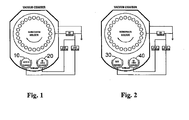
- FIG. 1 An example of single-cathode technology is described by means of figure 1 .
- the Al 0.885 Si 0.10 Cr 0.015 target 10 is used for the main layer preparation, the pure Cr target 20 is used for cleaning process and for adhesion and optional base layer system, alone or in combination with target 10.
- Electrode 30 consists of an AlSi alloy respectively pure Al, the metal electrode 40 is used for ion cleaning, to form the optional base layer, and is used, during the process, together with the AlSi (Al) to create the main Al 1-x Me x Si y N layer.
- the process becomes unstable.
- the arc voltage grows up - at a nitrogen pressure of 2 Pa, 100 A arc current - from 30 V to more than 40 V during the process which influences both process stability and coating quality.
- the addition of either or both, conductive nitrides and metallic conductive materials stabilize the evaporation process of AlSi respectively Al material in nitrogen or a nitrogen-based gas mixture atmosphere.
- the pure Al 1-y Si y N layer cross-section in comparison to an Al 1-x Cr x Si y N layer is shown on the figures 3 and 4 .
- the difference is considered being caused by insufficient conductivity of the layer during the process.
- the ion bombardment is not maintained which causes grain coarsening during film growth, resulting in bad mechanical properties.
- the increase of the arc voltage during the process has been measured to be no more than 1 V.
- the material shows no significant voltage increase at all during deposition resulting in a homogeneous structure, which yields good mechanical properties, i.e. wear resistance, important for the use of the coating.
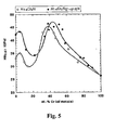
- Figure 5 shows the hardness dependence on coating stoichiometry for the system Al 1-x Cr x Si y N respectively Al 1-x Cr x N
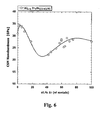
- Figure 6 Al 1-x Zr x Si y N shows another dopant possibility and a higher silicon content.
- Target 1 Cr (partially shielded)
- Target 2 Al 0.88 Si 0.12 alloy or blend
- Coating Al 0.85 Si 0.10 Cr 0.05 N
- Coating thickness 3.0 ⁇ m
- Process sequence Pumping to high vacuum P ⁇ 1x10⁻⁵ hPa Heating in vacuum to process temperature, e.g.
- Target 1 Ti Target 2 Al 0.90 Si 0.08 Cr 0.02 alloy or blend Coating: A1 0.91 Si 0.06 Cr 0.03 N Coating thickness: 2.5 ⁇ m
- Process sequence Pumping to high vacuum P ⁇ 1x10 -5 hPa Heating in vacuum to process temperature e.g.
- Target 1 Cr Target 2 A 0.82 Si 0.15 Cr 0.03 alloy or blend Coating : Al 0.84 Si 0.12 Cr 0.04 N Coating thickness: 4.0 ⁇ m
- Process sequence Pumping to high vacuum P ⁇ 1x10 -5 hPa Heating in vacuum to process temperature, e.g.
- Target 1 Zr (partially shielded)
- Target 2 Al 0.82 Si 0.18 alloy or blend
- Coating Al 0.835 Si 0.140 Zr 0.025 N Coating thickness 3.0 ⁇ m
- Process sequence Pumping to high vacuum P ⁇ 1x10 -5 hPa Heating in vacuum to process temperature, e.g.
- Example 5 Single-cathode sputter solution (sputter process with arc bonding layer)
- Target 1 Cr (arc target)
- Target 2 Al 0.82 Si 0.15 Cr 0.03 alloy or blend (sputter magnetron)
- Coating Al 0.81 Si 0.14 Cr 0.05 N
- Coating thickness 2.0 ⁇ m
- Process sequence Pumping to high vacuum P ⁇ 1x10 -5 hPa Heating in vacuum to process temperature, e.g.
Description
- The present invention relates to a hard, wear-resistant aluminum nitride based coating, an article coated there with and a method for producing such a coating.
- Layers based on Al1-xTixN respectively based on Al1-xTixSiyN are commonly used in a Ti/Al stoichiometry range near the maximum hardness. In the case of TiAlN, this stoichiometry corresponds approximately to Al0.65Ti0.35N. If an Al proportion exceeding these conditions, e.g. 75 to 85 at.% of metals, is selected, both hardness and wear resistance are known to break down rapidly. Essentially the same behaviour has been expected and found for Al1-xCrxN and similar hard materials.
- The existing knowledge about this softening is described in T. Suzuki, Y.Makino, M. Samandi and S. Miyake, J.Mater.Sci.35(2000), 4193 and A. Hörling, L. Hultman, M, Odén, J. Sjölén, L. Karlsson, Surf. Coat. Technol. 191 (2005) 384 and references cited therein.
- A typical coating is further known from
JP-A-2003/225809 -
US 5 580 653 discloses a hard coating having a composition given by the formula (AlxTi1-x-ySiy) (NzC1-z), where 0.05≤x≤0.75, 0.01≤y≤0.1, and 0.6≤z≤1. Said coating is formed on the surface of a substrate using e.g. an arc discharge ion-plating method. In the case that an arc discharge type method is employed, it is preferred that an ion-plating method in which the metal components Al, Ti an Si ionized from the cathode-vaporization source in an atmosphere of nitrogen gas and/or methane gas is used. If a target having the same composition as that desired for the hard coating ist used, a hard coating of a consistent composition can be obtained. If a bias voltage is applied to the substrate, the adhesion of the coating to the substrate can be further enhanced. -
EP 1 219 723 A2 - It is thus firstly the object of the invention to provide a hard coating which can be easily produced using cathodic arc evaporation technology and magnetron sputtering technology or a combination thereof.
- The invention achieves the object by a coating according to
Claim 1. The measures of the invention firstly have the result that an article can be coated by the hard coating according to the present invention using cathodic arc evaporation technology without further handling of the chamber in which the process is performed. Additionally, the coating is surprisingly hard with respect to the parameters. - The solution according to the present invention is based on the fact that at a further increase of the Al content of any Al1xMexN system substantially beyond the composition prior known as the maximum hardness, to approximately more than 90 at.% of the total of elements except nitrogen, the hardness has been surprisingly found rising again. Furthermore, this tendency has been found as being enhanced in the presence of silicon. However, very close to pure AlN or Al1-ySiyN, respectively, the layer hardness decreases again. This can be explained by the buildup of a non-conductive layer, resulting in the suppression of ion bombardment during deposition.
- Further details, features and advantages of the object of the invention are obtained from the following description of the relevant drawings wherein, for example, a method according to the present invention is explained.
- The drawings are as follows:
- Figure 1
- is a view of the schematic arrangement of the targets in the chamber according to a first example according to the present invention;
- Figure 2
- is a view of the schematic arrangement of the targets in the chamber according to a second example according to the present invention;
- Figure 3
- is a cross-sectional view of an Al0.91Si0.09N layer showing the undesired formation of a weak columnar coating material due to the lack of ion bombardment;
- Figure 4
- is a cross-sectional view of an Al0.86Si0.09Cr0.05N layer showing the homogeneous and consistently fine structure achieved by maintaining coating conductivity by doping with a small amount of metal (in this case Cr);
- Figure 5
- is the diagram of the hardness dependence on coating stoichiometry for the Al1-xCrxSi((1-x)/10)N system. Besides the main hardness maximum known already, an unexpected secondary hardness maximum is observed at very high (Al+Si) contents. The second curve (not this invention), of the comparison system Al1-xCrxN without silicon addition, shows a similar behaviour but generally lower hardness;
- Figure 6
- is the diagram of the hardness dependence on coating stoichiometry for the system Al1-xZrxSi((1-x)/5)N. This curve shows that the region below 8 at.% dopant addition even yields the global hardness for this system.
- Figure 7
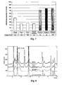
- is the diagram of metal drilling test using solid carbide drills of
diameter 5 mm, under the following testing conditions: Drilling of blind holes in coldworking steel X155CrVMo12-1 (DIN 1.2379) in soft annealed state, depth ofhole 15 mm, vc = 70 m/min, feed = 0.16 mm/rev, internal coolant emulsion 7%. - Figure 8
- is the grazing incidence X-ray diffraction diagram of a typical coating according to the present invention of composition Al0.834Si0.123Cr0.044N0.994, in as-deposited state and after thermal treatment at 800°C in nitrogen atmosphere for one hour. It illustrates the coexistance of both hexagonal and cubic phase in this system. The thermal stability of the nanocomposite crystallographic structure is proven by the similarity of the observed diffraction peaks before and after annealing at high temperatures.
- Layers were deposited predominantly by arc evaporation technology. AlN-based layers can be prepared from a single target or from several separated ones. The optimum layer is Al1-xMexSiyN, where the optimum Me content lies between 1 and 3 at.% and Si content between 3 and 10 at.% (this corresponds to x = 0.02 to 0.06 and y = 0.06 to 0.20).
- An example of single-cathode technology is described by means of
figure 1 . The Al0.885Si0.10Cr0.015target 10 is used for the main layer preparation, thepure Cr target 20 is used for cleaning process and for adhesion and optional base layer system, alone or in combination withtarget 10. - A two-cathode system is shown on
figure 2 .Electrode 30 consists of an AlSi alloy respectively pure Al, themetal electrode 40 is used for ion cleaning, to form the optional base layer, and is used, during the process, together with the AlSi (Al) to create the main Al1-xMexSiyN layer. - When the metal dopant content is chosen too low (significantly less than 1 at.%) the process becomes unstable. In the case of pure AlN respectively AlSiN layers with an Al respectively AlSi metallic purity of minimum 99.5 weight%, wherein the demonstrated impurity is mainly Fe, the arc voltage grows up - at a nitrogen pressure of 2 Pa, 100 A arc current - from 30 V to more than 40 V during the process which influences both process stability and coating quality. The addition of either or both, conductive nitrides and metallic conductive materials, stabilize the evaporation process of AlSi respectively Al material in nitrogen or a nitrogen-based gas mixture atmosphere. The pure Al1-ySiyN layer cross-section in comparison to an Al1-xCrxSiyN layer is shown on the
figures 3 and 4 . The difference is considered being caused by insufficient conductivity of the layer during the process. The ion bombardment is not maintained which causes grain coarsening during film growth, resulting in bad mechanical properties. In the case of a CrAl target at a presence of 1 atomic percent of Cr in Al, the increase of the arc voltage during the process has been measured to be no more than 1 V. At a presence of 3 atomic percent of Cr the material shows no significant voltage increase at all during deposition resulting in a homogeneous structure, which yields good mechanical properties, i.e. wear resistance, important for the use of the coating. -
Figure 5 shows the hardness dependence on coating stoichiometry for the system Al1-xCrxSiyN respectively Al1-xCrxN, andFigure 6 (Al1-xZrxSiyN) shows another dopant possibility and a higher silicon content. - A remarkable finding is that the hardness of these coatings stays stable and even increases upon annealing at temperatures above the deposition temperature, as shown in table 1.
- This stability can be explained by the two-phase structure of this material, which contains both hexagonal AlN phase and another, cubic phase (
Fig. 8 ). This nanocomposite system remains practically unchanged after annealing for one hour at 800°C in an inert atmosphere. This means an improvement for the use of such compounds as coatings for tooling applications, where high temperatures occur at the cutting edge.Table 1. Thermal stability of Al1-xCrxSiyN coatings on Hardmetal. The composition is given excluding nitrogen; the nitrogen content in all coatings was determined to be 50 ± 1 at.% by Rutherford backscattering Spectroscopy (RBS) analysis. Sample # at.% Al at.% Si at.% Cr Density [g/cm3] Nanohardness [GPa] as depos. annealed 800°C 703 90.5 6.1 3.4 2.7 40.5 40.9 763 83.4 12.3 4.4 3.1 38.7 40.8 759 84.2 12.2 3.7 3.3 37.3 38.9 767 83.6 12.3 4.1 3.6 37.3 38.8 117 76.9 17.3 4.8 3.7 38.3 39.5 - The process parameters of four examples as described above are shown in the following tables:
-
Configuration: Target 1 Cr (partially shielded)Target 2 Al0.88Si0.12 alloy or blendCoating: Al0.85Si0.10Cr0.05N Coating thickness: 3.0 µm Process sequence: Pumping to high vacuum P<1x10⁻⁵ hPa Heating in vacuum to process temperature, e.g. 450°C Ar plasma etching, Ar flow 200 sccm, bias -750 V, 2 min Arc metal ion etching, bias -1200 V, Cx arc 60A, Ar flow 15 sccm, 5 minAdhesion layer, CrN, Cr current 120 A, cathode 2 off P(N2)1x10⁻² hPa, bias -120 v, 5 minDeposition, AlSi current 130 A, Cr 50 A, P(N2) 3 x 10⁻² hPa, bias -75 V -
Configuration: Target 1Ti Target 2 Al0.90Si0.08Cr0.02 alloy or blend Coating: A10.91Si0.06Cr0.03N Coating thickness: 2.5 µm Process sequence: Pumping to high vacuum P<1x10⁻⁵ hPa Heating in vacuum to process temperature e.g. 450°C Ar plasma etching, Ar flow 200 sccm, bias -750 V, 2 min Arc metal ion etching, bias -900 V, 4 min, Cr arc 55 A, Ar flow 15 sccmAdhesion layer, TiN, current 125 A, P(N2) 1x10⁻² hPa, bias -120 V; cathode 2 off, 2 minDeposition AlSiCr 125 A, Ti off, P(N2) = 3x10⁻² hPa, bias -75 V Optional base layer before above deposition step: Ti current 120 A, cathode 2 off, P(N2) 1.0x10⁻² hPa, bias -75 V, 3 min -
Configuration: Target 1 CrTarget 2 A0.82Si0.15Cr0.03 alloy or blend Coating : Al0.84Si0.12Cr0.04N Coating thickness: 4.0 µm Process sequence: Pumping to high vacuum P<1x10⁻⁵ hPa Heating in vacuum to process temperature, e.g. 475°C Ar plasma etching, Ar flow 200 sccm, bias -750 V, 1 min Arc metal ion etching, bias -1000 V, 5 min, Cr arc 60 A, Ar flow 15 sccm;Adhesion layer (optional), CrN, Cr current 125 A, cathode 2 off, P(N2) 1x10⁻² hPa, bias -120 V, 2 minGraded interlayer, Al1-xCrxSi((1-x)/7)N, P(N2) 2x10⁻² hPa, bias -75 V; Cr 125 A -> 75 A, AlSiCr 75 -> 140 A, 5 min Deposition, AlSiCr 130 A, cathode 1 off, P(N2) = 5x10⁻² hPa, bias -40 V -
Configuration: Target 1 Zr (partially shielded)Target 2 Al0.82Si0.18 alloy or blendCoating: Al0.835Si0.140Zr0.025N Coating thickness 3.0 µm Process sequence: Pumping to high vacuum P<1x10⁻⁵ hPa Heating in vacuum to process temperature, e.g. 450°C Ar plasma etching, Ar flow 200 sccm, bias -750 V, 1min Arc metal ion etching, bias -1200 V, 5 min, Zr arc 70A, Ar flow 15 sccmAdhesion layer (optional), ZrN, Zr current 120 A, cathode 2 off, P(N2)1.8x10⁻² hPa, bias -120 V, 2 minGraded interlayer, Al1-xZrxSi((1-x)/5.2)N, P(N2) 2x10⁻² hPa, bias -60 V; Zr 125 A -> 60 A, AlSi 75 -> 140 A, 10 min Deposition AlSi current 140 A, Zr 60 A, P(N2) 2.5 x 10⁻² hPa, bias -60 V -
Configuration: Target 1 Cr (arc target)Target 2Al0.82Si0.15Cr0.03 alloy or blend (sputter magnetron) Coating: Al0.81Si0.14Cr0.05N Coating thickness: 2.0 µm Process sequence: Pumping to high vacuum P<1x10⁻⁵ hPa Heating in vacuum to process temperature, e.g. 400°C Ar plasma etching, Ar flow 200 sccm, bias -750 V, 1 min Arc metal ion etching, bias -1000 V, 5 min, Cr arc 60 A, Ar flow 15 sccmAdhesion layer (optional), CrN, Cr arc current 125 A, cathode 2 off, P(N2) 1x10⁻² hPa, bias -120 V, 2 minDeposition, AlSiCr magnetron sputter target 10 kW, cathode 1 (arc) off, P (Ar+N2) = 2.2x10⁻³ hPa, P(N2) - 5x10⁻⁴ hPa, bias -150 V. - It should be noted that the experimental conditions to execute the invention are generally disclosed in
WO-A-02/50865 EP-A-1357577 by the same applicant.
Claims (20)
- A hard, wear-resistant aluminum nitride based coating, consisting of a layer of composition AlxSiyMezN deposited on a substrate, wherein x, y and z denote atomic fractions, the sum of which is between 0.95 and 1.05, and wherein Me is a metal dopant of the group consisting of a member of group III to VIII and Ib transition metals or a combination of two or more of these members, said member providing an intrinsic electrical conductivity higher than the coating without said metal doping, wherein the silicon content is in between 0.01 ≤ y ≤ 0.4 and the content of the metal dopant or dopants Me is 0.001 ≤ z ≤ 0.08, preferably 0.01 ≤ z ≤ 0.05 and most preferably 0.015 ≤ z ≤ 0.045.
- The hard aluminum nitride based coating according to claim 1, where the metal dopant or dopant combination Me is a member of groups III to VI transition metals and Ce.
- The hard aluminum nitride based coating according to claim 1, where the metal dopant or dopant combination Me is a member of groups VII, VIII or Ib transition metals, and preferably of the first row of these groups (Mn, Fe, Co, Ni, Cu) and Ag.
- The hard aluminum nitride based coating according to any of claims 1 to 3, wherein said metal dopant or dopant combination Me is atomically distributed in the coating.
- The hard aluminum nitride based coating according to any of claims 1 to 4, wherein said metal dopant or dopant combination Me is contained in the coating in the form of its nitride compound.
- The hard aluminum nitride based coating according to any of claims 1 to 4, wherein said metal dopant or dopant combination Me is contained in the coating in the metallic form.
- The hard aluminum nitride based coating according to claims 1 to 6, characterized by a silicon content of 0.05 ≤ y ≤ 0.20.
- The hard aluminum nitride based coating according to any of claims 1 to 7, characterized in that it comprises an addition of up to 20 at.-% of one or more of the elements boron or carbon or oxygen.
- The hard aluminum nitride based coating according to any of claims 1 to 8, characterized in that the composition of the layer is chemically graded over the thickness with respect to at least one of the comprised elements.
- The hard aluminum nitride based coating according to any of claims 1 to 8, characterized in that it consists of a sequence of chemically different sublayers which together form a multilayered or nanolayered structure.
- The hard aluminum nitride based coating according to any of claims 1 to 10 characterized in that at least a part of the layer has a nanocomposite structure containing at least two phases.
- The hard aluminum nitride based coating according to any of claims 1 to 11, characterized by an adhesive interface layer deposited onto said substrate before depositing said layer of composition AlxSiyMezN, wherein said substrate is pretreated by a ion bombardment cleaning.
- The hard aluminum nitride based coating according to any of claims 1 to 12, characterized by a base layer of a conventional hard material comprising of a transition metal nitride, carbonitride or oxynitride which base layer' is deposited onto said substrate prior to the deposition of said layer of composition AlxSiyMezN.
- The hard aluminum nitride based coating according to claim 13, characterized in that said base layer is at least 0.3 µm thick and is chemically graded with respect to at least one of the constituents.
- An article comprising a hard aluminum nitride based coating according to any of claims 1 to 14, wherein the substrate consists of coldworking or HSS tool steels or hardmetals (WC/Co) or cermets or cubic boron nitride or PCD or an engineering ceramic, said article being suitable for tooling applications such as drilling, milling, turning, reaming, threadforming, hobbing etc.
- A method of depositing a coating according to any of claims 1 to 11, characterized in that said coating has been deposited using cathodic arc evaporation technology.
- A method of depositing a coating according to any of claims 1 to 11, characterized in that said coating has been deposited using magnetron sputtering technology
- A method of depositing a coating according to any of claims 1 to 11, characterized in that said coating has been deposited using a combination of cathodic arc evaporation and magnetron sputtering technology.
- The method according to any of claims 16 to 18, wherein said deposition is performed in a vacuum deposition chamber in which at least one cylindrical cathode is arranged.
- The method of any of claims 16 to 19, wherein during the coating process a DC, or unipolar pulsed DC, negative bias voltage is applied to the substrates to be coated and the surfaces of said substrates as well as of anodes and deposition chamber inner walls remain intrinsically conductive throughout the entire coating process duration.
Priority Applications (1)
| Application Number | Priority Date | Filing Date | Title |
|---|---|---|---|
| EP20050739548 EP1749118B1 (en) | 2004-04-19 | 2005-04-18 | A hard, wear-resistant aluminum nitride based coating |
Applications Claiming Priority (3)
| Application Number | Priority Date | Filing Date | Title |
|---|---|---|---|
| EP04405241 | 2004-04-19 | ||
| PCT/EP2005/003974 WO2005100635A1 (en) | 2004-04-19 | 2005-04-18 | A hard, wear-resistant aluminum nitride based coating |
| EP20050739548 EP1749118B1 (en) | 2004-04-19 | 2005-04-18 | A hard, wear-resistant aluminum nitride based coating |
Publications (2)
| Publication Number | Publication Date |
|---|---|
| EP1749118A1 EP1749118A1 (en) | 2007-02-07 |
| EP1749118B1 true EP1749118B1 (en) | 2014-04-09 |
Family
ID=34966976
Family Applications (1)
| Application Number | Title | Priority Date | Filing Date |
|---|---|---|---|
| EP20050739548 Not-in-force EP1749118B1 (en) | 2004-04-19 | 2005-04-18 | A hard, wear-resistant aluminum nitride based coating |
Country Status (7)
| Country | Link |
|---|---|
| US (1) | US7704611B2 (en) |
| EP (1) | EP1749118B1 (en) |
| JP (1) | JP5209960B2 (en) |
| KR (1) | KR101089528B1 (en) |
| CN (1) | CN100577874C (en) |
| CA (1) | CA2562402C (en) |
| WO (1) | WO2005100635A1 (en) |
Families Citing this family (26)
| Publication number | Priority date | Publication date | Assignee | Title |
|---|---|---|---|---|
| JP5192642B2 (en) * | 2005-11-11 | 2013-05-08 | 三菱重工業株式会社 | Surface covering member, method for manufacturing the same, tool, and machine tool |
| JP5096715B2 (en) * | 2006-09-21 | 2012-12-12 | 株式会社神戸製鋼所 | Hard coating and hard coating tool |
| CN101557897B (en) * | 2007-02-22 | 2011-09-07 | 三菱重工业株式会社 | Surface film member, process for rpoducing the surface covering member, cutting tool, and machine tool |
| IL191822A0 (en) * | 2007-06-25 | 2009-02-11 | Sulzer Metaplas Gmbh | Layer system for the formation of a surface layer on a surface of a substrate and also are vaporization source for the manufacture of a layer system |
| EP2022870B1 (en) * | 2007-06-25 | 2014-07-23 | Sulzer Metaplas GmbH | Layer system for creating a surface layer on a surface of a substrate, vaporisation source for manufacturing a layer system |
| EP2042261A3 (en) * | 2007-09-26 | 2015-02-18 | Sandvik Intellectual Property AB | Method of making a coated cutting tool |
| DE102008019891A1 (en) * | 2008-04-21 | 2009-10-22 | Mtu Aero Engines Gmbh | Erosion protection coating |
| ES2774167T3 (en) * | 2008-09-02 | 2020-07-17 | Oerlikon Surface Solutions Ag Pfaeffikon | Coating device for coating a substrate, as well as a method for coating a substrate |
| KR101608495B1 (en) | 2009-12-11 | 2016-04-01 | 삼성전자주식회사 | Apparatus and Method for processing data stream |
| CN102387676A (en) * | 2010-08-31 | 2012-03-21 | 鸿富锦精密工业(深圳)有限公司 | Shell body and manufacture method thereof |
| CN102586732A (en) * | 2011-01-17 | 2012-07-18 | 鸿富锦精密工业(深圳)有限公司 | Coated part with hard coating, and preparation method of coated part |
| CN102586731A (en) * | 2011-01-17 | 2012-07-18 | 鸿富锦精密工业(深圳)有限公司 | Coated part with hard coating and preparation method thereof |
| US8574728B2 (en) | 2011-03-15 | 2013-11-05 | Kennametal Inc. | Aluminum oxynitride coated article and method of making the same |
| EP2521159A1 (en) | 2011-05-06 | 2012-11-07 | Pivot a.s. | Glow discharge apparatus and method with lateral rotating arc cathodes |
| JP5559131B2 (en) * | 2011-11-22 | 2014-07-23 | 株式会社神戸製鋼所 | Hard coating and hard coating tool |
| CN104160060A (en) | 2012-03-07 | 2014-11-19 | 山高刀具公司 | A body with a metal based nitride layer and a method for coating the body |
| JP5417649B2 (en) * | 2012-05-08 | 2014-02-19 | 住友電工ハードメタル株式会社 | Surface coated cutting tool |
| US9126273B2 (en) | 2012-12-17 | 2015-09-08 | Kennametal Inc | Tool for the cutting machining of workpieces and process for coating substrate bodies |
| US9138864B2 (en) | 2013-01-25 | 2015-09-22 | Kennametal Inc. | Green colored refractory coatings for cutting tools |
| US9017809B2 (en) | 2013-01-25 | 2015-04-28 | Kennametal Inc. | Coatings for cutting tools |
| JP5764171B2 (en) * | 2013-08-07 | 2015-08-12 | 株式会社神戸製鋼所 | Conductive thin film |
| US9427808B2 (en) | 2013-08-30 | 2016-08-30 | Kennametal Inc. | Refractory coatings for cutting tools |
| JP6284726B2 (en) * | 2013-09-11 | 2018-02-28 | 太陽誘電株式会社 | Aluminum nitride film forming method, acoustic wave device manufacturing method, and aluminum nitride film manufacturing apparatus |
| DE102013018007A1 (en) * | 2013-11-29 | 2015-06-03 | Oerlikon Trading Ag, Trübbach | Method for improving the Gegenkörperverschleisses in tribological contact |
| CN104060230B (en) * | 2014-04-25 | 2017-06-06 | 湛江师范学院 | A kind of TiZrAlSiON nano composite super-hards coated cutting tool and preparation method thereof |
| CA3186105A1 (en) * | 2020-07-22 | 2022-01-27 | Dongfang Yang | Coated substrates and methods for the preparation thereof |
Family Cites Families (10)
| Publication number | Priority date | Publication date | Assignee | Title |
|---|---|---|---|---|
| JP2793773B2 (en) * | 1994-05-13 | 1998-09-03 | 神鋼コベルコツール株式会社 | Hard coating, hard coating tool and hard coating member excellent in wear resistance |
| TR200000710T2 (en) * | 1997-09-12 | 2000-09-21 | Balzers Aktiengesellschaft | A device with a protective layer system. |
| EP1017870B1 (en) * | 1997-09-12 | 2002-10-23 | Unaxis Balzers Aktiengesellschaft | Tool having a protective layer system |
| CZ296094B6 (en) | 2000-12-18 | 2006-01-11 | Shm, S. R. O. | Apparatus for evaporation of materials for coating of objects |
| ES2273772T3 (en) | 2000-12-28 | 2007-05-16 | Kabushiki Kaisha Kobe Seiko Sho | A HARD FILM FOR CUTTING TOOLS. |
| JP4112834B2 (en) * | 2000-12-28 | 2008-07-02 | 株式会社神戸製鋼所 | Target for forming hard coatings for cutting tools |
| JP3695396B2 (en) * | 2002-01-11 | 2005-09-14 | 三菱マテリアル神戸ツールズ株式会社 | Surface-coated cemented carbide cutting tool with excellent wear resistance in high-speed cutting of difficult-to-cut materials |
| JP3632667B2 (en) | 2002-02-01 | 2005-03-23 | 三菱マテリアル神戸ツールズ株式会社 | Surface-coated cemented carbide cutting tool with excellent wear resistance in high-speed cutting of difficult-to-cut materials |
| DK1357577T3 (en) | 2002-04-22 | 2008-06-02 | Pivot A S | Bow coating method with rotating cathodes |
| WO2005040448A1 (en) * | 2003-10-27 | 2005-05-06 | Mitsubishi Heavy Industries, Ltd. | Coating of high wear resistance and high hardness excelling in resistance to high temperature oxidation and, provided therewith, tool or metal mold of gear cutting machine tool |
-
2005
- 2005-04-18 CA CA 2562402 patent/CA2562402C/en not_active Expired - Fee Related
- 2005-04-18 EP EP20050739548 patent/EP1749118B1/en not_active Not-in-force
- 2005-04-18 CN CN200580011763A patent/CN100577874C/en not_active Expired - Fee Related
- 2005-04-18 JP JP2007508791A patent/JP5209960B2/en active Active
- 2005-04-18 KR KR1020067021755A patent/KR101089528B1/en active IP Right Grant
- 2005-04-18 US US11/568,088 patent/US7704611B2/en not_active Expired - Fee Related
- 2005-04-18 WO PCT/EP2005/003974 patent/WO2005100635A1/en active Application Filing
Also Published As
| Publication number | Publication date |
|---|---|
| CA2562402C (en) | 2011-10-11 |
| US20080318069A1 (en) | 2008-12-25 |
| KR20070012416A (en) | 2007-01-25 |
| EP1749118A1 (en) | 2007-02-07 |
| JP2007532783A (en) | 2007-11-15 |
| CA2562402A1 (en) | 2005-10-27 |
| US7704611B2 (en) | 2010-04-27 |
| KR101089528B1 (en) | 2011-12-05 |
| CN1942605A (en) | 2007-04-04 |
| JP5209960B2 (en) | 2013-06-12 |
| CN100577874C (en) | 2010-01-06 |
| WO2005100635A1 (en) | 2005-10-27 |
Similar Documents
| Publication | Publication Date | Title |
|---|---|---|
| EP1749118B1 (en) | A hard, wear-resistant aluminum nitride based coating | |
| EP3269479B1 (en) | Surface-coated cutting tool and method for manufacturing same | |
| EP3153259B1 (en) | Surface-coated tool and method for manufacturing same | |
| EP1791986B1 (en) | Cutting tool with wear resistant coating and method of making the same | |
| KR100937072B1 (en) | Hard coating having excellent wear resistance and oxidation resistance and target for forming the same, and hard coating having excellent high-temperature lubricating ability and wear resistance and target for forming the same | |
| EP2446987B1 (en) | Tool having coated cubic boron nitride sintered body | |
| EP1842610A1 (en) | Surface-coated cutting tool and process for producing the same | |
| JP2007532783A5 (en) | ||
| EP2340321B1 (en) | Non gamma - phase cubic alcro | |
| EP2201154B1 (en) | Method of producing a layer by arc-evaporation from ceramic cathodes | |
| EP3388546A1 (en) | Hard coating, hard coating-covered member and manufacturing method therefor, and target used for producing hard coating and manufacturing method therefor | |
| US9822438B2 (en) | Coated cutting tool and method for the production thereof | |
| JP2003113463A (en) | COATED MEMBER WITH TiAl ALLOY FILM AND MANUFACTURING METHOD THEREFOR | |
| JP5035980B2 (en) | Surface-coated cutting tool that exhibits high wear resistance with a hard coating layer in high-speed milling and a method for producing the same | |
| EP4316707A1 (en) | Coated cutting tool | |
| JP4968674B2 (en) | Surface-coated cutting tool with excellent chipping resistance and wear resistance with excellent hard coating layer in high-speed cutting and method for manufacturing the same | |
| JP3638332B2 (en) | Coated hard alloy | |
| JP5035979B2 (en) | Surface-coated cutting tool that exhibits high wear resistance with a hard coating layer in high-speed milling and a method for producing the same | |
| JPH06316756A (en) | Corrosion and wear resistant coating film | |
| JP2001219303A (en) | Surface-coated cemented carbide cutting tool with excellent wear resistance | |
| JP2001322004A (en) | Surface coated cemented carbide cutting tool with excellent wear resistance | |
| JP2003094208A (en) | MEMBER CLAD WITH FILM OF TiAl COMPOUND, AND MANUFACTURING METHOD THEREFOR | |
| JP2001219306A (en) | Surface-coated cemented carbide cutting tool with excellent wear resistance | |
| JPH10244406A (en) | Throwaway type cutting tip made of surface-covering cermet with its hard covering layer having excellent breakage resistance | |
| JP2001219305A (en) | Surface-coated cemented carbide cutting tool with excellent wear resistance |
Legal Events
| Date | Code | Title | Description |
|---|---|---|---|
| PUAI | Public reference made under article 153(3) epc to a published international application that has entered the european phase |
Free format text: ORIGINAL CODE: 0009012 |
|
| 17P | Request for examination filed |
Effective date: 20061113 |
|
| AK | Designated contracting states |
Kind code of ref document: A1 Designated state(s): AT BE BG CH CY CZ DE DK EE ES FI FR GB GR HU IE IS IT LI LT LU MC NL PL PT RO SE SI SK TR |
|
| RIN1 | Information on inventor provided before grant (corrected) |
Inventor name: MORSTEIN, MARCUS Inventor name: CODDET, OLIVIER Inventor name: SIMA, MICHAL Inventor name: JILEK, MOJMIR |
|
| DAX | Request for extension of the european patent (deleted) | ||
| 17Q | First examination report despatched |
Effective date: 20091021 |
|
| GRAP | Despatch of communication of intention to grant a patent |
Free format text: ORIGINAL CODE: EPIDOSNIGR1 |
|
| INTG | Intention to grant announced |
Effective date: 20131031 |
|
| GRAS | Grant fee paid |
Free format text: ORIGINAL CODE: EPIDOSNIGR3 |
|
| GRAA | (expected) grant |
Free format text: ORIGINAL CODE: 0009210 |
|
| AK | Designated contracting states |
Kind code of ref document: B1 Designated state(s): AT BE BG CH CY CZ DE DK EE ES FI FR GB GR HU IE IS IT LI LT LU MC NL PL PT RO SE SI SK TR |
|
| REG | Reference to a national code |
Ref country code: GB Ref legal event code: FG4D |
|
| REG | Reference to a national code |
Ref country code: DE Ref legal event code: R081 Ref document number: 602005043235 Country of ref document: DE Owner name: PLATIT AG, CH Free format text: FORMER OWNER: PIVOT A.S., SUMPERK, CZ |
|
| REG | Reference to a national code |
Ref country code: AT Ref legal event code: REF Ref document number: 661418 Country of ref document: AT Kind code of ref document: T Effective date: 20140415 Ref country code: CH Ref legal event code: EP |
|
| REG | Reference to a national code |
Ref country code: IE Ref legal event code: FG4D |
|
| REG | Reference to a national code |
Ref country code: DE Ref legal event code: R096 Ref document number: 602005043235 Country of ref document: DE Effective date: 20140522 |
|
| RAP2 | Party data changed (patent owner data changed or rights of a patent transferred) |
Owner name: PIVOT A.S. |
|
| PGFP | Annual fee paid to national office [announced via postgrant information from national office to epo] |
Ref country code: LU Payment date: 20140430 Year of fee payment: 10 |
|
| REG | Reference to a national code |
Ref country code: CH Ref legal event code: NV Representative=s name: R.A. EGLI AND CO, PATENTANWAELTE, CH |
|
| REG | Reference to a national code |
Ref country code: NL Ref legal event code: T3 |
|
| REG | Reference to a national code |
Ref country code: SE Ref legal event code: TRGR |
|
| REG | Reference to a national code |
Ref country code: LT Ref legal event code: MG4D |
|
| PG25 | Lapsed in a contracting state [announced via postgrant information from national office to epo] |
Ref country code: FI Free format text: LAPSE BECAUSE OF FAILURE TO SUBMIT A TRANSLATION OF THE DESCRIPTION OR TO PAY THE FEE WITHIN THE PRESCRIBED TIME-LIMIT Effective date: 20140409 Ref country code: BG Free format text: LAPSE BECAUSE OF FAILURE TO SUBMIT A TRANSLATION OF THE DESCRIPTION OR TO PAY THE FEE WITHIN THE PRESCRIBED TIME-LIMIT Effective date: 20140709 Ref country code: IS Free format text: LAPSE BECAUSE OF FAILURE TO SUBMIT A TRANSLATION OF THE DESCRIPTION OR TO PAY THE FEE WITHIN THE PRESCRIBED TIME-LIMIT Effective date: 20140809 Ref country code: GR Free format text: LAPSE BECAUSE OF FAILURE TO SUBMIT A TRANSLATION OF THE DESCRIPTION OR TO PAY THE FEE WITHIN THE PRESCRIBED TIME-LIMIT Effective date: 20140710 Ref country code: LT Free format text: LAPSE BECAUSE OF FAILURE TO SUBMIT A TRANSLATION OF THE DESCRIPTION OR TO PAY THE FEE WITHIN THE PRESCRIBED TIME-LIMIT Effective date: 20140409 |
|
| PG25 | Lapsed in a contracting state [announced via postgrant information from national office to epo] |
Ref country code: ES Free format text: LAPSE BECAUSE OF FAILURE TO SUBMIT A TRANSLATION OF THE DESCRIPTION OR TO PAY THE FEE WITHIN THE PRESCRIBED TIME-LIMIT Effective date: 20140409 Ref country code: PL Free format text: LAPSE BECAUSE OF FAILURE TO SUBMIT A TRANSLATION OF THE DESCRIPTION OR TO PAY THE FEE WITHIN THE PRESCRIBED TIME-LIMIT Effective date: 20140409 |
|
| PGFP | Annual fee paid to national office [announced via postgrant information from national office to epo] |
Ref country code: SE Payment date: 20140418 Year of fee payment: 10 |
|
| PG25 | Lapsed in a contracting state [announced via postgrant information from national office to epo] |
Ref country code: PT Free format text: LAPSE BECAUSE OF FAILURE TO SUBMIT A TRANSLATION OF THE DESCRIPTION OR TO PAY THE FEE WITHIN THE PRESCRIBED TIME-LIMIT Effective date: 20140811 |
|
| REG | Reference to a national code |
Ref country code: DE Ref legal event code: R097 Ref document number: 602005043235 Country of ref document: DE |
|
| REG | Reference to a national code |
Ref country code: IE Ref legal event code: MM4A |
|
| PG25 | Lapsed in a contracting state [announced via postgrant information from national office to epo] |
Ref country code: RO Free format text: LAPSE BECAUSE OF FAILURE TO SUBMIT A TRANSLATION OF THE DESCRIPTION OR TO PAY THE FEE WITHIN THE PRESCRIBED TIME-LIMIT Effective date: 20140409 Ref country code: BE Free format text: LAPSE BECAUSE OF FAILURE TO SUBMIT A TRANSLATION OF THE DESCRIPTION OR TO PAY THE FEE WITHIN THE PRESCRIBED TIME-LIMIT Effective date: 20140409 Ref country code: DK Free format text: LAPSE BECAUSE OF FAILURE TO SUBMIT A TRANSLATION OF THE DESCRIPTION OR TO PAY THE FEE WITHIN THE PRESCRIBED TIME-LIMIT Effective date: 20140409 Ref country code: MC Free format text: LAPSE BECAUSE OF FAILURE TO SUBMIT A TRANSLATION OF THE DESCRIPTION OR TO PAY THE FEE WITHIN THE PRESCRIBED TIME-LIMIT Effective date: 20140409 Ref country code: SK Free format text: LAPSE BECAUSE OF FAILURE TO SUBMIT A TRANSLATION OF THE DESCRIPTION OR TO PAY THE FEE WITHIN THE PRESCRIBED TIME-LIMIT Effective date: 20140409 Ref country code: EE Free format text: LAPSE BECAUSE OF FAILURE TO SUBMIT A TRANSLATION OF THE DESCRIPTION OR TO PAY THE FEE WITHIN THE PRESCRIBED TIME-LIMIT Effective date: 20140409 |
|
| PLBE | No opposition filed within time limit |
Free format text: ORIGINAL CODE: 0009261 |
|
| STAA | Information on the status of an ep patent application or granted ep patent |
Free format text: STATUS: NO OPPOSITION FILED WITHIN TIME LIMIT |
|
| 26N | No opposition filed |
Effective date: 20150112 |
|
| GBPC | Gb: european patent ceased through non-payment of renewal fee |
Effective date: 20140709 |
|
| REG | Reference to a national code |
Ref country code: FR Ref legal event code: PLFP Year of fee payment: 11 |
|
| REG | Reference to a national code |
Ref country code: DE Ref legal event code: R097 Ref document number: 602005043235 Country of ref document: DE Effective date: 20150112 |
|
| PG25 | Lapsed in a contracting state [announced via postgrant information from national office to epo] |
Ref country code: IE Free format text: LAPSE BECAUSE OF NON-PAYMENT OF DUE FEES Effective date: 20140418 |
|
| PG25 | Lapsed in a contracting state [announced via postgrant information from national office to epo] |
Ref country code: GB Free format text: LAPSE BECAUSE OF NON-PAYMENT OF DUE FEES Effective date: 20140709 |
|
| PGFP | Annual fee paid to national office [announced via postgrant information from national office to epo] |
Ref country code: NL Payment date: 20150420 Year of fee payment: 11 |
|
| PG25 | Lapsed in a contracting state [announced via postgrant information from national office to epo] |
Ref country code: SI Free format text: LAPSE BECAUSE OF FAILURE TO SUBMIT A TRANSLATION OF THE DESCRIPTION OR TO PAY THE FEE WITHIN THE PRESCRIBED TIME-LIMIT Effective date: 20140409 |
|
| PGFP | Annual fee paid to national office [announced via postgrant information from national office to epo] |
Ref country code: IT Payment date: 20150428 Year of fee payment: 11 Ref country code: FR Payment date: 20150421 Year of fee payment: 11 |
|
| PG25 | Lapsed in a contracting state [announced via postgrant information from national office to epo] |
Ref country code: LU Free format text: LAPSE BECAUSE OF NON-PAYMENT OF DUE FEES Effective date: 20150418 |
|
| REG | Reference to a national code |
Ref country code: SE Ref legal event code: EUG |
|
| PG25 | Lapsed in a contracting state [announced via postgrant information from national office to epo] |
Ref country code: SE Free format text: LAPSE BECAUSE OF NON-PAYMENT OF DUE FEES Effective date: 20150419 |
|
| PG25 | Lapsed in a contracting state [announced via postgrant information from national office to epo] |
Ref country code: CY Free format text: LAPSE BECAUSE OF FAILURE TO SUBMIT A TRANSLATION OF THE DESCRIPTION OR TO PAY THE FEE WITHIN THE PRESCRIBED TIME-LIMIT Effective date: 20140409 |
|
| PG25 | Lapsed in a contracting state [announced via postgrant information from national office to epo] |
Ref country code: TR Free format text: LAPSE BECAUSE OF FAILURE TO SUBMIT A TRANSLATION OF THE DESCRIPTION OR TO PAY THE FEE WITHIN THE PRESCRIBED TIME-LIMIT Effective date: 20140409 Ref country code: HU Free format text: LAPSE BECAUSE OF FAILURE TO SUBMIT A TRANSLATION OF THE DESCRIPTION OR TO PAY THE FEE WITHIN THE PRESCRIBED TIME-LIMIT; INVALID AB INITIO Effective date: 20050418 |
|
| PGFP | Annual fee paid to national office [announced via postgrant information from national office to epo] |
Ref country code: CZ Payment date: 20160418 Year of fee payment: 12 |
|
| PGFP | Annual fee paid to national office [announced via postgrant information from national office to epo] |
Ref country code: AT Payment date: 20160421 Year of fee payment: 12 |
|
| REG | Reference to a national code |
Ref country code: NL Ref legal event code: MM Effective date: 20160501 |
|
| REG | Reference to a national code |
Ref country code: FR Ref legal event code: ST Effective date: 20161230 |
|
| PG25 | Lapsed in a contracting state [announced via postgrant information from national office to epo] |
Ref country code: NL Free format text: LAPSE BECAUSE OF NON-PAYMENT OF DUE FEES Effective date: 20160501 Ref country code: FR Free format text: LAPSE BECAUSE OF NON-PAYMENT OF DUE FEES Effective date: 20160502 |
|
| PG25 | Lapsed in a contracting state [announced via postgrant information from national office to epo] |
Ref country code: IT Free format text: LAPSE BECAUSE OF NON-PAYMENT OF DUE FEES Effective date: 20160418 |
|
| REG | Reference to a national code |
Ref country code: AT Ref legal event code: MM01 Ref document number: 661418 Country of ref document: AT Kind code of ref document: T Effective date: 20170418 |
|
| PG25 | Lapsed in a contracting state [announced via postgrant information from national office to epo] |
Ref country code: AT Free format text: LAPSE BECAUSE OF NON-PAYMENT OF DUE FEES Effective date: 20170418 Ref country code: CZ Free format text: LAPSE BECAUSE OF NON-PAYMENT OF DUE FEES Effective date: 20170418 |
|
| REG | Reference to a national code |
Ref country code: DE Ref legal event code: R081 Ref document number: 602005043235 Country of ref document: DE Owner name: PLATIT AG, CH Free format text: FORMER OWNER: PIVOT A.S., SUMPERK, CZ Ref country code: DE Ref legal event code: R081 Ref document number: 602005043235 Country of ref document: DE Owner name: PLATIT A.S., CZ Free format text: FORMER OWNER: PIVOT A.S., SUMPERK, CZ |
|
| REG | Reference to a national code |
Ref country code: CH Ref legal event code: PFA Owner name: PLATIT A.S., CZ Free format text: FORMER OWNER: PIVOT A.S., CZ |
|
| REG | Reference to a national code |
Ref country code: DE Ref legal event code: R081 Ref document number: 602005043235 Country of ref document: DE Owner name: PLATIT A.S., CZ Free format text: FORMER OWNER: PLATIT AG, SELZACH, CH |
|
| PGFP | Annual fee paid to national office [announced via postgrant information from national office to epo] |
Ref country code: DE Payment date: 20190418 Year of fee payment: 15 |
|
| PGFP | Annual fee paid to national office [announced via postgrant information from national office to epo] |
Ref country code: CH Payment date: 20190730 Year of fee payment: 15 |
|
| REG | Reference to a national code |
Ref country code: CH Ref legal event code: NV Representative=s name: FREIGUTPARTNERS GMBH, CH |
|
| REG | Reference to a national code |
Ref country code: DE Ref legal event code: R119 Ref document number: 602005043235 Country of ref document: DE |
|
| REG | Reference to a national code |
Ref country code: CH Ref legal event code: PL |
|
| PG25 | Lapsed in a contracting state [announced via postgrant information from national office to epo] |
Ref country code: DE Free format text: LAPSE BECAUSE OF NON-PAYMENT OF DUE FEES Effective date: 20201103 Ref country code: LI Free format text: LAPSE BECAUSE OF NON-PAYMENT OF DUE FEES Effective date: 20200430 Ref country code: CH Free format text: LAPSE BECAUSE OF NON-PAYMENT OF DUE FEES Effective date: 20200430 |