EP1746655A2 - Optimiertes Verfahren zur Herstellung einer Bildaufnahmevorrichtung und Struktur zur Verbesserung des Überstrahlens - Google Patents
Optimiertes Verfahren zur Herstellung einer Bildaufnahmevorrichtung und Struktur zur Verbesserung des Überstrahlens Download PDFInfo
- Publication number
- EP1746655A2 EP1746655A2 EP06253647A EP06253647A EP1746655A2 EP 1746655 A2 EP1746655 A2 EP 1746655A2 EP 06253647 A EP06253647 A EP 06253647A EP 06253647 A EP06253647 A EP 06253647A EP 1746655 A2 EP1746655 A2 EP 1746655A2
- Authority
- EP
- European Patent Office
- Prior art keywords
- pixel array
- well
- pixels
- implant
- kev
- Prior art date
- Legal status (The legal status is an assumption and is not a legal conclusion. Google has not performed a legal analysis and makes no representation as to the accuracy of the status listed.)
- Withdrawn
Links
Images

Classifications
-
- H—ELECTRICITY
- H10—SEMICONDUCTOR DEVICES; ELECTRIC SOLID-STATE DEVICES NOT OTHERWISE PROVIDED FOR
- H10F—INORGANIC SEMICONDUCTOR DEVICES SENSITIVE TO INFRARED RADIATION, LIGHT, ELECTROMAGNETIC RADIATION OF SHORTER WAVELENGTH OR CORPUSCULAR RADIATION
- H10F39/00—Integrated devices, or assemblies of multiple devices, comprising at least one element covered by group H10F30/00, e.g. radiation detectors comprising photodiode arrays
- H10F39/011—Manufacture or treatment of image sensors covered by group H10F39/12
- H10F39/014—Manufacture or treatment of image sensors covered by group H10F39/12 of CMOS image sensors
-
- H—ELECTRICITY
- H10—SEMICONDUCTOR DEVICES; ELECTRIC SOLID-STATE DEVICES NOT OTHERWISE PROVIDED FOR
- H10F—INORGANIC SEMICONDUCTOR DEVICES SENSITIVE TO INFRARED RADIATION, LIGHT, ELECTROMAGNETIC RADIATION OF SHORTER WAVELENGTH OR CORPUSCULAR RADIATION
- H10F39/00—Integrated devices, or assemblies of multiple devices, comprising at least one element covered by group H10F30/00, e.g. radiation detectors comprising photodiode arrays
- H10F39/10—Integrated devices
- H10F39/12—Image sensors
- H10F39/18—Complementary metal-oxide-semiconductor [CMOS] image sensors; Photodiode array image sensors
- H10F39/186—Complementary metal-oxide-semiconductor [CMOS] image sensors; Photodiode array image sensors having arrangements for blooming suppression
-
- H—ELECTRICITY
- H10—SEMICONDUCTOR DEVICES; ELECTRIC SOLID-STATE DEVICES NOT OTHERWISE PROVIDED FOR
- H10F—INORGANIC SEMICONDUCTOR DEVICES SENSITIVE TO INFRARED RADIATION, LIGHT, ELECTROMAGNETIC RADIATION OF SHORTER WAVELENGTH OR CORPUSCULAR RADIATION
- H10F39/00—Integrated devices, or assemblies of multiple devices, comprising at least one element covered by group H10F30/00, e.g. radiation detectors comprising photodiode arrays
- H10F39/80—Constructional details of image sensors
- H10F39/807—Pixel isolation structures
Definitions
- Blooming is a bright light image artifact that affects both CCD and CMOS Image sensors.
- a scene with a bright region such as a reflection from a chrome bumper on a car
- blooming can occur in the captured image.
- the scene is imaged onto an array of pixels (such as on a CMOS or CCD image sensor)
- some of the pixels in the sensor receive the light from the bright region.
- the incident light is much more intense on those pixels than the other pixels of the imager that capture other aspects of the scene.
- the charge created by the photosensitive element e.g. photodiode, pinned photodiode, or photogate
- the image of the bright region appears larger in the image than it is in the actual scene. This apparent growth of a bright spot due to "blooming" is an issue with current CCD and CMOS image sensors.
- Optical blooming is a result of light scatter, reflection, and/or diffraction. In each of these cases light that is directed initially at a particular target pixel is actually received by an adjacent pixel due to the physical mechanisms of scattering, reflection, and/or diffraction.
- Electrical blooming refers to the diffusion of the charge (electron signal) from the target pixel to an adjacent pixel. When light (a photon) is received by a pixel, an electron-hole pair is created. Ideally the electron is stored in the target pixel photosensitive element. However, if that electron diffuses to an adjacent pixel, the result is blooming.
- Optical blooming can be improved by reducing the stack height of the image sensor so that the photosensitive element is closer to its micro-lens. Optical blooming can also be improved by using light shields to prevent photons from being scattered into adjacent pixels.
- Figure 1 shows a prior art four transistor (4T) pixel for a CMOS image sensor.
- two adjacent photosensitive elements (1) the target photosensitive element under the red color filter array (CFA) and (2) the adjacent photosensitive element under the blue CFA.
- STI shallow trench isolation
- a transfer gate, a reset gate, a floating diffusion, and a Vdd drain are also shown.
- These structures are formed on a P+ substrate over which there is a p-type epi layer.
- the STI isolation between pixels is typically 2000-5000 angstroms (A), usually about 3000 A deep.
- the P-well isolation between pixels is typically about 4500 A deep which can be achieved with about a 160 keV B11 implant.
- the epi thickness is typically about 8 microns thick.
- a lateral overflow drain LOD
- VOD vertical overflow drain
- a transistor or transistors that are connected to a positive voltage supply voltage, i.e., a current drain.
- a current drain a positive voltage supply voltage
- the electrons that overflow the capacity of the photosensitive element may result in a current through the adjacent transistors to the drain.
- a doping profile is created vertically under the photosensitive element.
- the electrons then flow over the barrier to the VOD drain.
- the formation of a VOD is a complicated process requiring additional masking and implants.
- the present invention provides an improved process that does not add the process complexity of a VOD but improves the blooming and cross-talk issues that remain in a LOD structure.
- the present invention provides a pixel array according to claim 1.
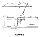
- Figure 2 illustrates an embodiment of the present invention that significantly improves blooming and color cross-talk.
- the present invention is effective for all CMOS and CCD image sensors, including but not limited to 3T, 4T, and 5T CMOS image sensors and interline or frame transfer CCD image sensors.
- Figure 2 is similar to Figure 1, except that according to the present invention, Figure 2 shows a pixel array using isolation that is a combination of a thin epi of thickness 2-6 microns and a deep P-well (DPW) implant process with B I 1 implant energies of greater than or equal to 700 keV.
- DPW deep P-well
- the p+ substrate is "brought into play" and is used as an electron barrier to prevent electron migration.
- the STI is the same as in the prior art, but it is to be understood that the STI may also be modified to be deeper.
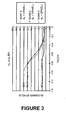
- Figure 3 shows experimental data that verifies the significance of having both a DPW and a thin epi.
- a bright image is focused on one half of an array of pixels. Under low light conditions a sharp demarcation is recorded between the bright and dark region.
- the light intensity is increased well beyond the pixel saturation level (e.g. 100X - 1000X saturation)
- the bright image blooms into the adjacent pixels.
- the lateral extent of the blooming is measured and recorded as the y-value in Figure 3.
- the higher the value on the y-axis the greater the blooming.
- Figure 3 shows the lateral extent of the blooming measured in 3.18 micron pixels as a function of the low voltage on the transfer gate (Vtx_lo) during integration. At very negative transfer gate voltages, the transfer gate is turned off, and the result is substantial blooming. At Vtx_lo voltages approaching 0 volts, the transfer gate is closer to being turned on during integration, and both the output signal (not shown) is reduced and the blooming is reduced.
- samples 64066-2 and 64067-2 in addition to the standard, shallow 1.5E13 B11 P-well implant at 180 keV, there are additional deep P-well implants at higher implant energies to improve blooming and cross-talk.
- Table 1 The specific parameters of each sample are summarized in Table 1. Note that all doses quoted herein are in units of ions/cm 2 . Samples 64066-5 and 64066-2 are both formed on 8 micron epi and sample 64067 uses a 4 micron epi.
- the data points corresponding to 64066-5 shows the blooming performance for the case of an image sensor made from a thick 8 micron epi and a shallow P-well (SPW) using a 1.5E13 B11 implant at 180 keV. In this case, the bright image blooms 14 pixels (44 u) laterally into the dark region.
- SPW shallow P-well
- a DPW has been added to the 8u epi. The DPW is formed by adding the following 3 implants: 3E12 B11 at 420 keV + 1E13 B11 at 800 keV + 1E13 B11 at 1.3 MeV. The result is only a slight reduction in blooming from 14 pixels to 12 pixels in the negative Vtx_lo region.
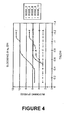
- Figure 4 shows a more careful study on the reduction of blooming as a function of the DPW implant conditions, all using a 4 micron epi.
- the standard PWell implant at 180 keV there are additional deep P-well implants to improve blooming and cross-talk as summarized in Table 2 below.
- the reference sample in Figure 4 is 80095-2 which is a single standard 2E13 B11 shallow P-well at 180 keV.
- Sample 80095-4 has a 3E12 B11 420 keV implant added and the lateral extent of the blooming is decreased.
- Sample 80095-10 then adds a 700 keV B11 implant but only at a 1E12 dose. This does not further significantly improve the blooming.
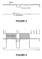
- Figures 5 and 6 describe a method for forming a pixel in accordance with one embodiment of the present invention.
- an epitaxial material is deposited onto a p-type substrate.
- the thickness of the epi is generally between 3 and 5 microns thick, but may be up to 6 microns thick as noted above. It has been found that an epi thickness of between 3 and 4.5 microns works well.
- Active areas and STI oxide isolation is formed as is conventional in the art.
- a thin oxide, typically termed a pad oxide or a sacrificial oxide or a gate oxide is formed over the epi layer.
- a thick deep ultraviolet (DUV) or 1-line resist of sufficient thickness to block the highest energy P-well implant is then coated onto the wafer.
- the photoresist is patterned as shown in Fig 6.
- the photosensitive element regions have thick resist remaining over those regions.
- the photoresist is removed.
- a series of deep P-well implants is performed to achieve the optimized blooming and cross-talk performance.
- the deep P-well implants should contain at least one implant that is equal to or greater than 700 keV. This provides a deep p-well depth of about 1.2 microns.
- the 1.3 MeV implant will generally produce a deep p-well depth of about 1.9 microns.
- the implant dose should also be equal to or greater than 3E12 ions/cm2.
- the words “comprise,” “comprising,” and the like are to be construed in an inclusive sense, as opposed to an exclusive or exhaustive sense; that is to say, in the sense of "including, but not limited to.”
- the terms “connected,” “coupled,” or any variant thereof means any connection or coupling, either direct or indirect, between two or more elements; the coupling of connection between the elements can be physical, logical, or a combination thereof.
Landscapes
- Solid State Image Pick-Up Elements (AREA)
- Element Separation (AREA)
Applications Claiming Priority (2)
| Application Number | Priority Date | Filing Date | Title |
|---|---|---|---|
| US70172505P | 2005-07-22 | 2005-07-22 | |
| US11/210,996 US20070018264A1 (en) | 2005-07-22 | 2005-08-24 | Optimized image sensor process and structure to improve blooming |
Publications (2)
| Publication Number | Publication Date |
|---|---|
| EP1746655A2 true EP1746655A2 (de) | 2007-01-24 |
| EP1746655A3 EP1746655A3 (de) | 2008-02-20 |
Family
ID=37177814
Family Applications (1)
| Application Number | Title | Priority Date | Filing Date |
|---|---|---|---|
| EP06253647A Withdrawn EP1746655A3 (de) | 2005-07-22 | 2006-07-12 | Optimiertes Verfahren zur Herstellung einer Bildaufnahmevorrichtung und Struktur zur Verbesserung des Überstrahlens |
Country Status (3)
| Country | Link |
|---|---|
| US (1) | US20070018264A1 (de) |
| EP (1) | EP1746655A3 (de) |
| TW (1) | TW200717783A (de) |
Cited By (3)
| Publication number | Priority date | Publication date | Assignee | Title |
|---|---|---|---|---|
| FR2918795A1 (fr) * | 2007-07-12 | 2009-01-16 | St Microelectronics Sa | Capteur d'images a sensibilite amelioree. |
| EP2228825A3 (de) * | 2009-03-09 | 2012-05-23 | Sony Corporation | Festkörperabbildungsvorrichtung, elektronisches Gerät und Herstellungsverfahren für die Festkörperabbildungsvorrichtung |
| US20210375964A1 (en) * | 2019-02-28 | 2021-12-02 | Samsung Electronics Co., Ltd. | Image sensor |
Families Citing this family (8)
| Publication number | Priority date | Publication date | Assignee | Title |
|---|---|---|---|---|
| JP4391497B2 (ja) * | 2006-05-19 | 2009-12-24 | シャープ株式会社 | カラーセンサー、カラーセンサーの製造方法、センサー、及び電子機器 |
| US8440495B2 (en) * | 2007-03-06 | 2013-05-14 | Taiwan Semiconductor Manufacturing Company, Ltd. | Method for reducing crosstalk in image sensors using implant technology |
| US9117725B2 (en) | 2010-04-09 | 2015-08-25 | Scint-X Ab | Pixel structures for optimized x-ray noise performance |
| KR101734936B1 (ko) * | 2010-08-27 | 2017-05-15 | 삼성전자주식회사 | 소자분리 막 아래에 저 저항 영역을 갖는 반도체 소자 |
| US8664734B2 (en) * | 2011-01-11 | 2014-03-04 | Himax Imaging, Inc. | Hole-based ultra-deep photodiode in a CMOS image sensor and a process thereof |
| US9070802B2 (en) * | 2013-08-16 | 2015-06-30 | Himax Imaging, Inc. | Image sensor and fabricating method of image sensor |
| JP6305028B2 (ja) * | 2013-11-22 | 2018-04-04 | キヤノン株式会社 | 光電変換装置の製造方法および光電変換装置 |
| US10418402B2 (en) * | 2017-11-30 | 2019-09-17 | Stmicroelectronics (Research & Development) Limited | Near ultraviolet photocell |
Family Cites Families (8)
| Publication number | Priority date | Publication date | Assignee | Title |
|---|---|---|---|---|
| JP2625602B2 (ja) * | 1991-01-18 | 1997-07-02 | インターナショナル・ビジネス・マシーンズ・コーポレイション | 集積回路デバイスの製造プロセス |
| JP2825004B2 (ja) * | 1991-02-08 | 1998-11-18 | インターナショナル・ビジネス・マシーンズ・コーポレーション | 側壁電荷結合撮像素子及びその製造方法 |
| US20030211701A1 (en) * | 2002-05-07 | 2003-11-13 | Agere Systems Inc. | Semiconductor device including an isolation trench having a dopant barrier layer formed on a sidewall thereof and a method of manufacture therefor |
| US7091536B2 (en) * | 2002-11-14 | 2006-08-15 | Micron Technology, Inc. | Isolation process and structure for CMOS imagers |
| US7087944B2 (en) * | 2003-01-16 | 2006-08-08 | Micron Technology, Inc. | Image sensor having a charge storage region provided within an implant region |
| JP3621400B2 (ja) * | 2003-03-03 | 2005-02-16 | 松下電器産業株式会社 | 固体撮像装置およびその製造方法 |
| US6897082B2 (en) * | 2003-06-16 | 2005-05-24 | Micron Technology, Inc. | Method of forming well for CMOS imager |
| US20060180885A1 (en) * | 2005-02-14 | 2006-08-17 | Omnivision Technologies, Inc. | Image sensor using deep trench isolation |
-
2005
- 2005-08-24 US US11/210,996 patent/US20070018264A1/en not_active Abandoned
-
2006
- 2006-06-29 TW TW095123673A patent/TW200717783A/zh unknown
- 2006-07-12 EP EP06253647A patent/EP1746655A3/de not_active Withdrawn
Cited By (8)
| Publication number | Priority date | Publication date | Assignee | Title |
|---|---|---|---|---|
| FR2918795A1 (fr) * | 2007-07-12 | 2009-01-16 | St Microelectronics Sa | Capteur d'images a sensibilite amelioree. |
| EP2228825A3 (de) * | 2009-03-09 | 2012-05-23 | Sony Corporation | Festkörperabbildungsvorrichtung, elektronisches Gerät und Herstellungsverfahren für die Festkörperabbildungsvorrichtung |
| US8975667B2 (en) | 2009-03-09 | 2015-03-10 | Sony Corporation | Solid-state imaging device, electronic equipment and manufacturing method of the solid-state imaging device |
| US20210375964A1 (en) * | 2019-02-28 | 2021-12-02 | Samsung Electronics Co., Ltd. | Image sensor |
| US20230253430A1 (en) * | 2019-02-28 | 2023-08-10 | Samsung Electronics Co., Ltd. | Image sensor |
| US11843016B2 (en) * | 2019-02-28 | 2023-12-12 | Samsung Electronics Co., Ltd. | Image sensor |
| US12094907B2 (en) * | 2019-02-28 | 2024-09-17 | Samsung Electronics Co., Ltd. | Image sensor |
| US12543396B2 (en) | 2019-02-28 | 2026-02-03 | Samsung Electronics Co., Ltd. | Image sensor having improved electrical and/or optical characteristics |
Also Published As
| Publication number | Publication date |
|---|---|
| EP1746655A3 (de) | 2008-02-20 |
| US20070018264A1 (en) | 2007-01-25 |
| TW200717783A (en) | 2007-05-01 |
Similar Documents
| Publication | Publication Date | Title |
|---|---|---|
| EP2282345B1 (de) | Bildsensor mit einem Übertragungsgate mit mehreren Kanalunterregionen | |
| US7705380B2 (en) | Amplification-type solid-state image sensing device | |
| US7901974B2 (en) | Masked laser anneal during fabrication of backside illuminated image sensors | |
| US9698185B2 (en) | Partial buried channel transfer device for image sensors | |
| US6713796B1 (en) | Isolated photodiode | |
| US7285438B2 (en) | Solid-state imaging device and method for manufacturing solid-state imaging device | |
| CN102177586B (zh) | 具有低串扰及高红色灵敏度的图像传感器 | |
| US8809925B2 (en) | Partial buried channel transfer device in image sensors | |
| JP3530159B2 (ja) | 固体撮像装置およびその製造方法 | |
| US7651883B2 (en) | High energy implant photodiode stack | |
| EP1746655A2 (de) | Optimiertes Verfahren zur Herstellung einer Bildaufnahmevorrichtung und Struktur zur Verbesserung des Überstrahlens | |
| WO2006124701A1 (en) | Color pixels with anti-blooming isolation and method of formation | |
| CN101252140B (zh) | 固体摄像装置以及摄像装置 | |
| US7736937B2 (en) | Manufacturing method of solid-state imaging device and solid-state imaging device | |
| JP2008034836A (ja) | 固体撮像素子 | |
| US20060163617A1 (en) | Solid-state imaging device and its manufacturing method | |
| US7948018B2 (en) | Multilayer image sensor structure for reducing crosstalk | |
| CN101238584A (zh) | 使用延伸的埋入触点来减少成像器串扰和像素噪声 | |
| JP2004031878A (ja) | 固体撮像装置 | |
| CN100517740C (zh) | 具有优化图像浮散性能的图像传感器结构及工艺方法 | |
| JP2002164529A (ja) | 固体撮像素子およびその製造方法 | |
| JPH08264747A (ja) | コンテナ側方オーバーフロードレインインプラントを有する固体画像化器及びその製造方法 | |
| JP4025208B2 (ja) | 固体撮像素子およびその製造方法 | |
| KR100624341B1 (ko) | 시시디 고체촬상소자 | |
| JPH08227989A (ja) | 固体撮像素子 |
Legal Events
| Date | Code | Title | Description |
|---|---|---|---|
| PUAI | Public reference made under article 153(3) epc to a published international application that has entered the european phase |
Free format text: ORIGINAL CODE: 0009012 |
|
| 17P | Request for examination filed |
Effective date: 20060801 |
|
| AK | Designated contracting states |
Kind code of ref document: A2 Designated state(s): AT BE BG CH CY CZ DE DK EE ES FI FR GB GR HU IE IS IT LI LT LU LV MC NL PL PT RO SE SI SK TR |
|
| AX | Request for extension of the european patent |
Extension state: AL BA HR MK YU |
|
| PUAL | Search report despatched |
Free format text: ORIGINAL CODE: 0009013 |
|
| AK | Designated contracting states |
Kind code of ref document: A3 Designated state(s): AT BE BG CH CY CZ DE DK EE ES FI FR GB GR HU IE IS IT LI LT LU LV MC NL PL PT RO SE SI SK TR |
|
| AX | Request for extension of the european patent |
Extension state: AL BA HR MK YU |
|
| AKX | Designation fees paid |
Designated state(s): AT BE BG CH CY CZ DE DK EE ES FI FR GB GR HU IE IS IT LI LT LU LV MC NL PL PT RO SE SI SK TR |
|
| STAA | Information on the status of an ep patent application or granted ep patent |
Free format text: STATUS: THE APPLICATION HAS BEEN WITHDRAWN |
|
| 18W | Application withdrawn |
Effective date: 20090518 |