EP1732165B1 - Antennenstruktur für mobile Kommunikationsendgeräte - Google Patents
Antennenstruktur für mobile Kommunikationsendgeräte Download PDFInfo
- Publication number
- EP1732165B1 EP1732165B1 EP05011708A EP05011708A EP1732165B1 EP 1732165 B1 EP1732165 B1 EP 1732165B1 EP 05011708 A EP05011708 A EP 05011708A EP 05011708 A EP05011708 A EP 05011708A EP 1732165 B1 EP1732165 B1 EP 1732165B1
- Authority
- EP
- European Patent Office
- Prior art keywords
- ground plane
- antenna structure
- exciter element
- feed line
- structure according
- Prior art date
- Legal status (The legal status is an assumption and is not a legal conclusion. Google has not performed a legal analysis and makes no representation as to the accuracy of the status listed.)
- Expired - Lifetime
Links
Images


Classifications
-
- H—ELECTRICITY
- H01—ELECTRIC ELEMENTS
- H01Q—ANTENNAS, i.e. RADIO AERIALS
- H01Q9/00—Electrically-short antennas having dimensions not more than twice the operating wavelength and consisting of conductive active radiating elements
- H01Q9/04—Resonant antennas
- H01Q9/0407—Substantially flat resonant element parallel to ground plane, e.g. patch antenna
- H01Q9/0421—Substantially flat resonant element parallel to ground plane, e.g. patch antenna with a shorting wall or a shorting pin at one end of the element
-
- H—ELECTRICITY
- H01—ELECTRIC ELEMENTS
- H01Q—ANTENNAS, i.e. RADIO AERIALS
- H01Q1/00—Details of, or arrangements associated with, antennas
- H01Q1/12—Supports; Mounting means
- H01Q1/22—Supports; Mounting means by structural association with other equipment or articles
- H01Q1/24—Supports; Mounting means by structural association with other equipment or articles with receiving set
- H01Q1/241—Supports; Mounting means by structural association with other equipment or articles with receiving set used in mobile communications, e.g. GSM
- H01Q1/242—Supports; Mounting means by structural association with other equipment or articles with receiving set used in mobile communications, e.g. GSM specially adapted for hand-held use
- H01Q1/243—Supports; Mounting means by structural association with other equipment or articles with receiving set used in mobile communications, e.g. GSM specially adapted for hand-held use with built-in antennas
-
- H—ELECTRICITY
- H01—ELECTRIC ELEMENTS
- H01Q—ANTENNAS, i.e. RADIO AERIALS
- H01Q5/00—Arrangements for simultaneous operation of antennas on two or more different wavebands, e.g. dual-band or multi-band arrangements
- H01Q5/30—Arrangements for providing operation on different wavebands
- H01Q5/307—Individual or coupled radiating elements, each element being fed in an unspecified way
- H01Q5/342—Individual or coupled radiating elements, each element being fed in an unspecified way for different propagation modes
- H01Q5/357—Individual or coupled radiating elements, each element being fed in an unspecified way for different propagation modes using a single feed point
Definitions
- the invention relates to an antenna structure for mobile communication terminals having an active ground plane for generating a current density distribution relevant for radiation of the electromagnetic waves and an exciter element capacitively coupled to the ground plane, the ground plane being substantially rectangular with two short and two long sides is trained.
- Such an antenna structure in which the radiation / reception element, unlike, for example, in the case of the known PIFA antennas, is formed by the ground plane is known, for example, from the article " Compact Antenna Structures for Mobile Handsets ", by Juha Villanen et al., Published on the occasion of the 3rd COST 284 Management Committee Meeting Workshop, Budapest, October 2003 , known.
- Theoretical background for such an antenna structure can also be found in the article " Resonator-Based Analysis of the Mobile Antenna and Chassis Handset ", by B. Vainikainen et al., Published in IEEE Trans. Antennas Propagation, Vol. 50, No. 10, pp. 1433-1444, October 2002 ,
- a stimulator element capacitively coupled to the printed circuit board is used to produce the desired current density distribution.
- the capacitively coupled stimulator element is disposed on a short side of the printed circuit board and lies substantially within a plane defined by the printed circuit board.
- the object of the invention is to improve the above-mentioned antenna structure such that a more effective excitation of the current density distribution of the ground plane is achieved.
- EP 1 079 463 A2 discloses an antenna structure with two exciter elements arranged in a plane next to each other.
- EP 1 494 315 A1 discloses an antenna structure with two exciter elements arranged in two parallel planes.
- JP 2000 156607 discloses an antenna system having an inner receiving element and an outer transmitting element arranged in a common plane.
- WO 2004/109850 A1 discloses a variable frequency variable reactance antenna.
- an antenna structure for mobile communication terminals having an active ground plane for forming a current density distribution relevant for radiation of electromagnetic waves and an exciter element which is capacitively coupled to the ground plane, wherein the ground plane is formed essentially at right angles with two short and two long sides, wherein the Anregerelement is flat, is arranged perpendicular to the ground plane and a short side of the ground plane adjacent and is connected via a feed line to the ground plane.
- Such an arrangement of the exciter element has the consequence that it thus reaches the area of locally maximum electric field strength of a chassis propagation mode and, for a given ground plane, it can be traversed by the largest possible electrical flux of the associated field distribution.
- a particularly strong coupling to the ground plane which can be formed by a ground layer of a printed circuit board, is achieved.
- This in turn means a particularly low radiation quality and thus a particularly high bandwidth for the resonance behavior of the ground plane.
- a capacitive load element approximately in the middle of the short side of the ground plane, which is opposite to the short side with adjacent exciter element, is electrically conductively connected to the ground plane.
- the dimensions of a circuit board are specified as a ground plane by other boundary conditions, this is advantageous, namely if a capacitive loading element is provided on that short side of the ground plane which is opposite the short side with adjacent exciter element, which is suitable for adapting a current density distribution of the ground plane adapted to a desired resonant frequency band.
- a capacitive loading element is provided on that short side of the ground plane which is opposite the short side with adjacent exciter element, which is suitable for adapting a current density distribution of the ground plane adapted to a desired resonant frequency band.
- an increase of an electrical length with regard to the mobile radio frequency bands GSM850 and GSM900 can be brought about by means of capacitive end load by the load element.
- the high-frequency frequency bands for DCS and PCS can be achieved by the inventive design of the loading element at the same time a reduction in the effective electrical length.
- the loading element is designed and arranged such that for the ground plane in the longitudinal direction of the Anregerelement from an electrical length, corresponding to half a desired resonant wavelength adjusts, at the end by means of the loading element a node line of the current density distribution is enforced and is further achieved the parallel to the longitudinal axis of the ground plane oriented current density at the ground plane and loading element beyond the node line in total is very small on average.
- closed slots are formed between the loading element and the ground plane, each with a length which corresponds to a quarter of a wavelength of a target frequency.
- the corners of the short side of the ground plane adjacent to the exciter element are chamfered.
- Such a “sharpening" of the ground plane causes a concentration of a distribution of electric charge in the middle region of this short side of the mass plane.
- the excitation element is also located approximately in the middle of the short side, a much larger portion of the electrical flux from that charge passes through the excitation element, which in turn results in a stronger stimulator element to ground plane coupling, lower radiation quality, and greater bandwidth
- a further advantageous embodiment provides, alternatively or additionally, in the middle region of the short side of the ground plane, which faces the exciter element, a surface mounted perpendicular thereto, which likewise supports the concentration of the charge in the central region.
- the excitation element is divided into an inner stimulator element section for a higher frequency spectral band and an outer stimulator element section for a lower frequency spectral band.
- the two Anregerelementabitese are electrically separated from each other by a circumferential gap, wherein at one point a web for mechanical retention of the outer Anregerelementabitess may remain.
- the outer stimulator element section may support the mobile radio frequency bands GSM850 and GSM900 while the inner stimulator element section is associated with the higher frequency frequency bands for DCS and PCS having their center frequencies at 1800 and 1900 MHz, respectively.
- a separate, leading to the ground plane feed line may be provided, each with separate feed points. This allows a separate supply line for the low-frequency and the higher-frequency spectral band, wherein a coupling can take place in particular from the inner Anregerelementabites to the outer.
- the feed line preferably has an inserted impedance whose value can be switched over or continuously adjusted, for example an inductance which can be connected.
- the feedline may be implemented in stripline technology, and a portion of the feedline may have a switchable feedline width.
- a switchable supply line width can be realized in that the supply line is slotted centrally in the section and one of the feeder line halves is provided with a switch. By closing the switch, the inductance can be changed from a previous non-switched state. This is preferably done by adjusting, for example, by reducing the inductance from the GSM850 band to the GSM900 band.
- the adaptation has effects on the resonant frequencies of the feed line and excitation element unit.
- both provided supply lines can be provided with such variable series impedance, so that it is possible to switch independently both within the lower-frequency spectrum and within the higher-frequency spectral band.
- the exciter structure for the higher-frequency band can be switched, for example, between the settings DCS and PCS band on the one hand and PCS band and UMTS band on the other.
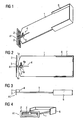
- the in the FIGS. 1 to 4 fully illustrated antenna structure has a ground plane 1, which may be, for example, a ground layer of a typical used in mobile phones electrical circuit board, which is the carrier of the required electrical components to support the functionality of the mobile phone.
- the ground plane 1 is capacitively coupled to an exciter element A1 which is divided into an outer exciter element section 2 and an inner exciter element section 3.
- the stimulator element A1 is arranged substantially perpendicular to a plane, which is spanned by the ground plane 1.
- the inner Anregerelementabites 3 is formed elongated long and is enclosed by the outer Anregerelementabterrorism 2, leaving a gap.
- the outer stimulator element section 2 serves to support lower-frequency mobile radio frequency bands, for example GSM850 and GSM900, while the inner stimulator element section 3 is designed for the frequency bands lying at 1800 and 1900 MHz for DCS and PCS.
- the two Anregerelementabitese 2, 3 can be considered as substantially independently operable Anregerium.
- the antenna structure could also be dispensed with the division of the Anregerelements A1 in the Anregerelementabête 2 and 3 and a common exciter for all bands are used.
- the division is advantageous on the one hand with regard to the decoupling of the feed points for the low-frequency and the higher-frequency spectral band, on the other hand with regard to the possibility of being able to tune the resonators formed by the exciter elements together with their feed lines largely unaffected by electrical switching elements.
- the ground plane 1 has beveled corners 1a on the short side, which is assigned to the exciter element A1, which cause the charge located in the adjacent area of the ground plane 1 to generate an electrical flux which efficiently passes through the excitation element A.
- the inner Anregerelementabites 3 is connected via a feed line 5 to the ground plane 1, which means that the feed line 5 is connected on the part of the electrical circuit board at one end point with the ground layer.
- the feed line 5 extends over the ground plane 1, this applies in the illustrated embodiment only partially for the feed line 4 for the outer Anregerelementabites 2, because it is led out at a point perpendicular to the ground plane 1 and then parallel to the ground plane 1 to the outer Stimulator element section 2 connected.
- This special cable routing is not of great importance for a function of the antenna structure.
- the feed line 4 could also be arranged on the dielectric (the ground plane 1).
- the likewise unbalanced feed point 4 a is again in the distance defined by the desired input impedance from the end point of the line 4 connected to the ground plane 1.
- Anregerelementabitese 2, 3 are arranged adjacent to a first short side of the ground plane 1, starting from the other short side of the ground surface 1, a loading element 6 is provided, which is electrically conductively connected to the ground surface 1 approximately in the middle of this short side.
- the loading element 6 serves in the present embodiment to shorten the effective electrical length of the ground plane 1 with respect to the DCS and PCS bands, while at the same time an increase in the electrical length for GSM850 and GSM900 is to be achieved by means of capacitive end load.
- the reduction of the electrical length for the DCS and PCS bands is achieved by having a node line L for the current density distribution of the ground plane 1 at a distance of an effective half wavelength from the short side of the ground plane 1 adjacent to the exciter element sections 2, 3 , is produced. (see. FIG. 7 ).
- the loading element 6 by forming a gap 7 on both sides of the ground surface 1 a resonant Shield, wherein the slot 7 corresponds to a quarter wavelength and for this reason in the illustrated embodiment in each case extends around a corner of the ground plane 1 around.
- the quarter wave parasitic resonators thus realized are substantially non-radiative due to the opposite directions of the current density vectors on the shielding load element 6 and the ground plane 1.
- the quarter wave parasitic resonators can be expected to incur only small dissipative losses.
- the effective electrical length for the use of the ground plane 1 as a radiating surface for the high-frequency bands PCS and DCS is therefore formed by a portion of the ground plane 1, which lies between the Anregerelementabroughen 2, 3 and the near ends of the slots 7.
- the loading element 6 acts as a capacitive end load for increasing the electrical length.
- the in FIG. 7 illustrated node line is not off.
- the loading element 6 affords the advantage that a dipole-like omnidirectional characteristic can be achieved both in the low-frequency and in the high-frequency spectral bands, which in the latter case is due to the resonant shielding by the loading element 6.
- FIG. 5 is a portion T1 from the said region of the feed line 4 partially shown schematically.
- the feed line 4 is slotted centrally over a distance, so that the Feeder 4 is divided into two halves.
- One half H1 is continuous, while the other half H2 is switchable by means of a switch S. In this way, an effective conductor width in the section T can be tuned by operating the switch S.
- the switch S By closing or opening the switch, the effective conductor width and thus the inductance of the portion T1 is changed, wherein the inductance and the conductor width are in first approximation inversely proportional to each other. In contrast, a capacity of the portion T1 remains substantially unchanged.
- the resonance frequency of the combination of feed line 4 and stimulator element section 2 can be changed, in particular an adaptation to the GSM850 or the GSM900 band can be brought about.
- the switch S can also be designed as a varactor, wherein in generalization of the procedure just described the series impedance of the section T1 is changed. The introduction of the switch or varactor into the feed line offers the advantage that only a relatively low HF voltage drops across the switching element.
- a power loss in the switching element is reduced by, for example, 6 dB in comparison to the case that the total current would be switched.
- a similar portion may also be provided in the feed line 5 for the high-frequency bands DCS and PCS.
- section T1 of the feed line 4 is allowed to comply with a non-linearity of the components available as switching elements pertinent specifications of the support mobile standards in terms of emission mask and emission of harmonics.
- FIG. 8 are now each a dependency between an input reflection factor at the feed point 4a of the line 4 and 5a of the line 5 and the frequency shown graphically.
- the solid lines are respectively assigned to the tuning position for GSM850 and the dashed lines to the tuning position for GSM900. With respect to the feed point 4a, reflection minima at 850 MHz and 900 MHz are readily found, depending on the tuning position.
- FIGS. 9, 10 an alternative embodiment of the antenna structure is shown, wherein an alternative excitation element A2 is shown together with an adjacent part of the ground plane 1.
- the stimulator element A2 essentially corresponds to the stimulator element section 2 for the mobile radio standards GSM850 and GSM900, but is divided along a plane that runs perpendicular to the ground plane 1 and contains a longitudinal axis of the ground plane 1.
- a feed line 8 which essentially runs like the feed line 4, extends over a section from the exciter element A2, which corresponds in length to about a quarter of a wavelength of a target frequency, divided. This creates a dipole that can be excited independently of other mobile bands.
- the excitation of the dipole takes place symmetrically at a feed point 8a of the symmetrically slotted supply line in a higher-frequency band while the excitation for GSM850 and GSM900 as described above continues to take place asymmetrically at a feed point 8b of the feed line 8 corresponding to the feed point 4a.
- the short side of the ground plane 1, which faces the exciter element A2 has slots 10 which extend, for example, approximately from the middle of the short side of the ground plane 1 toward the respective long sides and slightly along the respective long sides a slot length is achieved which corresponds approximately to a quarter wave resonance at the higher frequency excitation frequency of the dipole.
- the task of these resonant slots 10 is not to short-circuit the electrical dipole field through the ground plane 1 by means of the split configuration of the feed line 8 and of the exciter element A2.
- the above-explained antenna structures according to the FIGS. 1 to 4 are distinguished by a considerable reduction in the quality of radiation compared to conventional solutions, the immediate consequence of which is a considerable increase in bandwidth.
- a quad-band prototype with less than three cm 3 antenna volume (exciter element volume) has already been implemented on an electrical circuit board with a total area of 100 mm ⁇ 40 mm, with a total thickness of the structure of the antenna structure of only 10 mm.
- the arrangement of the Anregerelementabroughe 2,3 and the extended alternative embodiment of the Anregerelements A2 in the described vertical nature to the ground plane 1 also has the advantage that the entire electrical circuit board remains free on both sides for the placement of other electronic components.
Landscapes
- Engineering & Computer Science (AREA)
- Computer Networks & Wireless Communication (AREA)
- Waveguide Aerials (AREA)
- Support Of Aerials (AREA)
- Transceivers (AREA)
Description
- Die Erfindung bezieht sich auf eine Antennenstruktur für mobile Kommunikationsendgeräte mit einer aktiven Masseebene zur Erzeugung einer für eine Abstrahlung der elektromagnetischer Wellen maßgeblichen Stromdichteverteilung und einem Anregerelement, das kapazitiv an die Masseebene gekoppelt ist, wobei die Masseebene im Wesentlichen rechtwinkelig mit zwei kurzen und zwei langen Seiten ausgebildet ist.
- Eine solche Antennenstruktur, bei der das Abstrahlungs-/Empfangselement, anders als beispielsweise bei den bekannten PIFA-Antennen, von der Masseebene gebildet wird, ist beispielsweise aus dem Fachartikel "Compact Antenna Structures for Mobile Handsets", von Juha Villanen et al., veröffentlicht anlässlich des "3rd COST 284 Management Committee Meeting Workshop", Budapest, Oktober 2003, bekannt. Theoretische Hintergründe für eine solche Antennenstruktur finden sich außerdem in dem Fachartikel "Resonator-Based Analysis of the Combination of Mobile Handset Antenna and Chassis", von B. Vainikainen et al., erschienen in IEEE Trans. Antennas Propagation, Vol. 50, Nr. 10, Seiten 1433 - 1444, Oktober 2002.
- Dieser Antennenstruktur ist es eigentümlich, dass eine für die Abstrahlung maßgebliche Stromdichteverteilung auf einer gedruckten Schaltkreisplatine eines Mobiltelefons bzw. auf einem Chassis des Mobiltelefons selbst angeregt wird. Anstelle einer "Antenne" im herkömmlichen Sinne wird zum Erzeugen der gewünschten Stromdichteverteilung ein kapazitiv an die gedruckte Schaltkreisplatine gekoppeltes Anregerelement verwendet. Beispielsweise in dem oben erstgenannten Fachartikel wird vorgeschlagen, für die beiden Mobilfunk-Standardfrequenzbereiche GSM900 und GSM1800 jeweils eine gesonderte Antennenstruktur vorzusehen. Dort ist das kapazitiv angekoppelte Anregerelement an einer kurzen Seite der gedruckten Schaltkreisplatine angeordnet und liegt im Wesentlichen innerhalb einer von der gedruckten Schaltkreisplatine aufgespannten Ebene. In dem GSM900 Frequenzband wurde für eine Reflexionsdämpfung von 10 dB für das GSM900-Frequenzband eine Bandbreite von 50 MHz und im GSM1800-Frequenzband eine Bandbreite von 95 MHz erreicht. Es handelte sich dabei jeweils um separate Strukturen. Eine Lösung, das genannte Prinzip der kapazitiven Anregung in einer gemeinsamen Struktur für zwei weit auseinanderliegende Frequenzbänder zu realisieren, ist bisher nicht bekannt.
- Ausgehend hiervon liegt der Erfindung die Aufgabe zugrunde, die eingangs genannte Antennenstruktur derart zu verbessern, dass eine effektivere Anregung der Stromdichteverteilung der Masseebene erzielt wird.
-
EP 1 079 463 A2 offenbart eine Antennenstruktur mit zwei Anregerelementen, die in einer Ebene neben einander liegend angeordnet sind. -
EP 1 494 315 A1 offenbart eine Antennenstruktur mit zwei Anregerelementen, die in zwei parallelen Ebenen angeordnet sind. -
JP 2000 156607 -
WO 2004/109850 A1 offenbart eine frequenzvariable Antenne mit variabler Reaktanz. - Diese Aufgabe wird gelöst durch eine Antennenstruktur mit den Merkmalen des Anspruchs 1.
- Danach ist vorgesehen eine Antennenstruktur für mobile Kommunikationsendgeräte mit einer aktiven Masseebene zur Ausbildung einer für eine Abstrahlung elektromagnetischer Wellen maßgeblichen Stromdichteverteilung und einem Anregerelement, das kapazitiv an die Masseebene gekoppelt ist, wobei die Masseebene im Wesentlichen rechtwinklig mit zwei kurzen und zwei langen Seiten ausgebildet ist, wobei das Anregerelement flach ausgebildet ist, senkrecht zu der Masseebene und einer kurzen Seite der Masseebene benachbart angeordnet ist und über eine Speiseleitung mit der Masseebene verbunden ist.
- Eine solche Anordnung des Anregerelementes hat die Folge, dass es damit in den Bereich lokal maximaler elektrischer Feldstärke einer Chassis-Ausbreitungsmode gelangt und bei gegebener Masseebene vom größtmöglichen elektrischen Fluss der zugehörigen Feldverteilung durchsetzt werden kann. Auf diese Weise wird eine besonders starke Kopplung an die Masseebene, die von einer Masse-Schicht einer gedruckten Schaltkreisplatine gebildet werden kann, erreicht. Dies wiederum bedeutet, eine besonders geringe Strahlungsgüte und damit eine besonders hohe Bandbreite für das Resonanzverhalten der Masseebene.
- Erfindungsgemäß ist ein kapazitives Belastungselement etwa in der Mitte der kurzen Seite der Masseebene, welche der kurzen Seite mit benachbartem Anregerelement gegenüberliegt, mit der Masseebene elektrisch leitend verbunden ist.
- Wenn beispielsweise die Abmessungen einer Schaltkreisplatine als Masseebene durch andere Randbedingungen vorgegeben sind, ist dies von Vorteil, nämlich wenn auf derjenigen kurzen Seite der Masseebene, welche der kurzen Seite mit benachbarten Anregerelement gegenüberliegt, ein kapazitives Belastungselement vorgesehen ist, das zur Anpassung einer Stromdichteverteilung der Masseebene an eine gewünschtes Resonanzfrequenzband angepasst ist. Auf diese Weise kann insbesondere ein Vergrößern einer elektrischen Länge im Hinblick auf die Mobilfunk-Frequenzbänder GSM850 und GSM900 mit Hilfe kapazitiver Endbelastung durch das Belastungselement herbeigeführt werden. Im Hinblick auf die hochfrequenten Frequenzbänder für DCS und PCS kann dabei durch die erfindungsgemäße Gestaltung des Belastungselementes gleichzeitig eine Verringerung der wirksamen elektrischen Länge erzielt werden. Dazu ist das Belastungselement derart ausgebildet und angeordnet, dass sich für die Masseebene in deren Längsrichtung von dem Anregerelement aus eine elektrische Länge, entsprechend einer halben gewünschten Resonanzwellenlänge, einstellt, an deren Ende vermittels des Belastungselementes eine Knotenlinie der Stromdichteverteilung erzwungen wird und ferner erreicht wird dass die parallel zur Längsachse der Masseebene orientierte Stromdichte auf Masseebene und Belastungselement jenseits der Knotenlinie insgesamt im Mittel sehr klein wird.
- Ferner ist es erfindungsgemäß vorgesehen, dass zwischen dem Belastungselement und der Masseebene geschlossene Schlitze jeweils mit einer Länge ausgebildet sind, die einem Viertel einer Wellenlänge einer Zielfrequenz entspricht.
- Bevorzugt sind die Ecken der kurzen Seite der Masseebene, die dem Anregerelement benachbart ist, abgeschrägt. Ein solches "Anspitzen" der Massefläche bewirkt eine Konzentration einer Verteilung elektrischer Ladung im mittleren Bereich dieser kurzen Seite der Massenebene. Wenn das Anregerelement ebenfalls etwa in der Mitte der kurzen Seite angeordnet ist, durchsetzt ein wesentlich größerer Teil des von dieser Ladung ausgehenden elektrischen Flusses das Anregerelement, was wiederum eine stärkere Kopplung zwischen Anregerelement und Masseebene, eine geringere Strahlungsgüte und eine dadurch größere Bandbreite zur Folge hat. Eine weitere vorteilhafte Ausführungsform sieht alternativ oder zusätzlich im mittleren Bereich der kurzen Seite der Masseebene, welche dem Anregerelement zugewandt ist eine senkrecht dazu angebrachte Fläche vor, die ebenfalls die Konzentration der Ladung im mittleren Bereich unterstützt.
- Zur Unterstützung zweier verschiedener Mobilfunk-Frequenzbereiche, beispielsweise der Bereich für GSM850 und GSM900 einerseits und DCS und PCS andererseits ist es von Vorteil, wenn das Anregerelement in einen inneren Anregerelementabschnitt für ein höherfrequentes Spektralband und einen äußeren Anregerelementabschnitt für ein niedrigerfrequentes Spektralband aufgeteilt ist. Dabei sind dann die beiden Anregerelementabschnitte elektrisch durch einen umlaufenden Spalt voneinander getrennt, wobei an einer Stelle ein Steg zur mechanischen Halterung des äußeren Anregerelementabschnitts verbleiben kann.
- In dieser Weise kann der äußere Anregerelementabschnitt zur Unterstützung der Mobilfunkfrequenzbänder GSM850 und GSM900 dienen, während der innere Anregerelementabschnitt den höherfrequenten Frequenzbändern für DCS und PCS zugeordnet ist, die ihre Mittenfrequenzen bei 1800 bzw. 1900 MHz haben.
- Für jeden der Anregerelementabschnitte kann eine gesonderte, zu der Masseebene führende Speiseleitung mit jeweils separaten Speisepunkten vorgesehen sein. Dies ermöglicht eine getrennte Zuleitung für das niederigerfrequente und das höherfrequente Spektralband, wobei eine Kopplung insbesondere von dem inneren Anregerelementabschnitt zu dem äußeren stattfinden kann.
- Bevorzugt weist die Speiseleitung eine eingefügte Impedanz auf, deren Wert umschaltbar oder kontinuierlich einstellbar ist, z.B. eine Induktivität, die zuschaltbar ist. Für dieses Ausführungsbeispiel kann die Speiseleitung in Streifenleitungstechnik ausgeführt sein und ein Teilstück der Speiseleitung kann eine umschaltbare Speiseleitungsbreite aufweisen. Eine solche umschaltbare Speiseleitungsbreite kann dadurch realisiert sein, dass in dem Teilstück die Speiseleitung mittig geschlitzt und eine der Speiseleitungshälften mit einem Schalter versehen ist. Durch Schließen des Schalters kann die Induktivität gegenüber einem vorhergehenden nicht zugeschalteten Zustands verändert werden. Dies geschieht bevorzugt derart, dass beispielsweise durch Verringerung der der Induktivität von dem GSM850-Band auf das GSM900-Band angepasst wird. Die Anpassung hat Auswirkungen für die Resonanzfrequenzen der Einheit aus Speiseleitung und Anregungselement. Selbstverständlich können bei aufgeteiltem Anregerelement beide vorgesehenen Speiseleitungen mit derart variabler Serienimpedanz versehen sein, so dass sowohl innerhalb des niedrigerfrequenten als auch innerhalb des höherfrequenten Spektralbandes unabhängig umgeschaltet werden kann. Die Anregerstruktur für das höherfrequente Band kann dabei beispielsweise zwischen den Einstellungen DCS- und PCS-Band einerseits und PCS-Band und UMTS-Band andererseits umgeschaltet werden.
- Ausführungsbeispiele der Erfindung werden nachfolgend anhand der Zeichnungen noch näher erläutert. Es zeigen:
- Figur 1
- eine perspektivische Ansicht einer Antennenstruktur mit zwei Anregerelementabschnitten, einer Masseebene und einem Belastungselement,
- Figur 2
- eine Draufsicht der Antennenstruktur von
Figur 1 , - Figur 3
- eine Seitenansicht der Antennenstruktur von
Figur 1 , - Figur 4
- eine weitere perspektivische Ansicht der Antennenstruktur von
Fig. 1 , - Figur 5
- eine Ansicht eines Teilstücks einer Speiseleitung der Antennenstruktur nach
Figur 1 , - Figur 6
- eine Aufsicht auf eine Metallisierungsstruktur im Bereich der Anregerelementabschnitte für die Antennenstruktur von
Figur 1 , - Figur 7
- eine Draufsicht der Antennenstruktur von
Figur 1 mit Darstellung einer elektrischen Stromdichteverteilung bei Anregung im höherfrequenten Band, - Figur 8
- eine graphische Darstellung einer Abhängigkeit zweier Eingangsreflexionsfaktoren an zwei Speisepunkten der Antennenstruktur von
Figur 1 als Funktion der Frequenz, - Figur 9
- eine Draufsicht auf ein alternatives Anregerelement, welches zusätzlich einen Diversity-Betrieb ermöglicht, und
- Figur 10
- eine Seitenansicht des Anregerelementes von
Figur 9 . - Die in den
Figuren 1 bis 4 vollständig dargestellte Antennenstruktur weist eine Masseebene 1 auf, bei der es sich beispielsweise um eine Masse-Schicht einer bei Mobiltelefonen typischer Weise eingesetzten elektrischen Schaltkreisplatine handeln kann, die Träger der erforderlichen elektrischen Baugruppen zur Unterstützung der Funktionalitäten des Mobiltelefons ist. Die Masseebene 1 ist kapazitiv mit einem Anregerelement A1 gekoppelt, welches in einen äußeren Anregerelementabschnitt 2 und einen inneren Anregerelementabschnitt 3 aufgeteilt ist. Das Anregerelement A1 ist im Wesentlichen senkrecht zu einer Ebene angeordnet, welche von der Masseebene 1 aufgespannt wird. Dabei ist der innere Anregerelementabschnitt 3 lang gestreckt ausgebildet und wird von dem äußeren Anregerelementabschnitt 2 unter Freilassung eines Spaltes umschlossen. Der äußere Anregerelementabschnitt 2 dient zur Unterstützung von niedrigerfrequenten Mobilfunk-Frequenzbändern, beispielsweise GSM850 und GSM900, während der innere Anregerelementabschnitt 3 für die bei 1800 bzw. 1900 MHz liegenden Frequenzbänder für DCS und PCS ausgelegt ist. Insofern können die beiden Anregerelementabschnitte 2, 3 als im Wesentlichen unabhängig voneinander betreibbare Anregerelemente aufgefasst werden. - Bei einem vereinfachten Ausführungsbeispiel der Antennenstruktur könnte auch auf die Teilung des Anregerelements A1 in die Anregerelementabschnitte 2 und 3 verzichtet werden und ein gemeinsamer Anreger für alle Bänder verwendet werden. Vorteilhaft ist die Teilung zum einen in Hinblick auf die Entkopplung der Speisepunkte für das niederfrequente und das höherfrequente Spektralband, zum anderen in Hinblick auf die Möglichkeit, die durch die Anregerelemente zusammen mit ihren Speiseleitungen gebildeten Resonatoren weitgehendst unbeeinflusst voneinander durch elektrische Schaltelemente abstimmen zu können. Von grundsätzlicher Bedeutung ist jedoch die im Wesentlichen senkrechte Anordnung der Anregerelementabschnitte 2, 3, welche zur Folge hat, dass sie in den Bereich einer lokal maximalen elektrischen Feldstärke einer abstrahlenden Stromdichteverteilung auf der Masseebene 1 gelangen und damit vom größtmöglichen elektrischen Fluss der zugehörigen Feldstärkeverteilungen durchsetzt werden. Ergebnis ist, dass eine besonders starke Kopplung zwischen den Anregerelementabschnitten 2, 3 und den gewünschten Stromdichteverteilungen auf der Masseebene 1 herbeigeführt wird, was eine erwünschte, geringe Strahlungsgüte mit hoher Bandbreite nach sich zieht.
- Die Masseebene 1 weist an derjenigen kurzen Seite, die dem Anregerelement A1 zugeordnet ist, abgeschrägte Ecken 1a auf, die bewirken, dass die in dem angrenzenden Bereich der Massefläche 1 befindliche Ladung einen elektrischen Fluss erzeugt, der das Anregerelement A effizient durchsetzt.
- Wie insbesondere aus
Figur 1 deutlich hervorgeht, ist der innere Anregerelementabschnitt 3 über eine Speiseleitung 5 mit der Masseebene 1 verbunden, was im Einzelnen heißt, dass die Speiseleitung 5 auf Seiten der elektrischen Schaltkreisplatine an einem Endpunkt mit deren Masseschicht verbunden ist. In dem durch die angestrebte Eingangsimpedanz definierten Abstand von diesem Endpunkt befindet sich ein unsymmetrische Speisepunkt 5a. Während die Speiseleitung 5 über der Masseebene 1 verläuft, gilt dies in dem dargestellten Ausführungsbeispiel nur teilweise für die Speiseleitung 4 für den äußeren Anregerelementabschnitt 2, denn sie ist an einer Stelle senkrecht zu der Masseebene 1 herausgeführt und dann parallel zu der Masseebene 1 an den äußeren Anregerelementabschnitt 2 angeschlossen. Diese spezielle Leitungsführung ist für eine Funktion der Antennenstruktur nicht von hoher Bedeutung. Die Speiseleitung 4 könnte ebenso auf dem Dielektrikum (der Masseebene 1) angeordnet sein. Der ebenfalls unsymmetrische Speisepunkt 4a befindet sich wiederum in dem durch die angestrebte Eingangsimpedanz definierten Abstand von dem mit der Masseebene 1 verbundenen Endpunkt der Leitung 4. - Aus der
Figur 7 geht zudem die Ausbildung einer einem elektrischen Dipol entsprechenden resonanten Stromdichteverteilung von der Knotenlinie L bis zu der dem Anregerelement A1 zugewandten kurzen Seite der Massefläche 1 hervor, wenn die Anregung im höherfrequenten Spektralband erfolgt, wobei diese Stromdichteverteilung für die Strahlungscharakteristik der Antennenstruktur maßgeblich ist. - Es ist darauf hinzuweisen, dass durch die Zweiteilung des Anregungselementes A1 in die Anregerelementabschnitte 2, 3 in der gewählten Anordnung eine Anregung sowohl im hochfrequenten als auch im niedrigfrequenten Bereich ermöglicht wird, weitestgehend ohne gegenseitige Beeinflussung. Dabei wird eine kapazitive Kopplung zwischen dem inneren Anregerelementabschnitt 3 und dem äußeren Anregerelementabschnitt 2 gezielt ausgenutzt, um eine größere effektive Fläche für die hochfrequenten Frequenzbänder wie DCS und PCS bereitzustellen. Dabei koppelt der innere Anregerelementabschnitt 3, der für die hochfrequenten Bänder wirksam ist, teilweise direkt auf die Masseebene 1 und teilweise indirekt, unter Zwischenschaltung des äußeren Anregerelementabschnitts 2 mit der Masseebene 1. Ein wesentlicher Vorteil dieser Lösung gegenüber einer multiresonanten Antennenstruktur besteht darin, dass aufgrund der elektrischen Abstimmbarkeit in beiden Bändern, d. h. dem niedrigfrequenten Spektralband und dem hochfrequenten Spektralband, jeweils höhere Nutzbandbreiten erreichbar sind, als es sonst möglich wäre.
- Während die Anregerelementabschnitte 2, 3 einer ersten kurzen Seite der Massefläche 1 benachbart angeordnet sind, ist ausgehend von der anderen kurzen Seite der Massefläche 1 ein Belastungselement 6 vorgesehen, das etwa in der Mitte dieser kurzen Seite elektrisch leitend mit der Massefläche 1 verbunden ist.
- Das Belastungselement 6 dient im vorliegenden Ausführungsbeispiel zur Verkürzung der wirksamen elektrischen Länge der Masseebene 1 im Hinblick auf die DCS- und PCS-Bänder, während gleichzeitig eine Vergrößerung der elektrischen Länge für GSM850 und GSM900 mittels kapazitiver Endbelastung erreicht werden soll. Die Verringerung der elektrischen Länge für das DCS- und das PCS-Band wird dadurch erreicht, dass eine Knotenlinie L für die Stromdichteverteilung der Masseebene 1 in einem Abstand einer effektiven Halbwellenlänge von der kurzen Seite der Masseebene 1, der die Anregerelementabschnitte 2, 3 benachbart sind, erzeugt wird. (vgl.
Figur 7 ). Zu diesem Zweck bewirkt das Belastungselement 6 durch Ausbildung eines Spaltes 7 zu beiden Seiten der Massefläche 1 eine resonante Abschirmung, wobei der Schlitz 7 einer Viertelwellenlänge entspricht und aus diesem Grunde im dargestellten Ausführungsbeispiel jeweils um eine Ecke der Masseebene 1 herum verläuft. Die derart realisierten parasitären Viertelwellenresonatoren sind im Wesentlichen nicht strahlend aufgrund der entgegensetzten Richtungen der Stromdichtevektoren auf dem abschirmend wirkenden Belastungselement 6 und der Masseebene 1. Für die parasitären Viertelwellenresonatoren kann erwartet werden, dass sie nur geringe dissipative Verluste mit sich bringen. - Die effektive elektrische Länge für die Benutzung der Massefläche 1 als Abstrahlungsfläche für die hochfrequenten Bänder PCS und DCS wird daher von einem Anteil der Massefläche 1 gebildet, der zwischen den Anregerelementabschnitten 2, 3 und den nahen Enden der Schlitze 7 liegt.
- Im Hinblick auf die niedrigfrequenten Spektralbänder für die Mobilfunk-Standards GSM850 und GSM900 wirkt das Belastungselement 6 als kapazitive Endbelastung zur Vergrößerung der elektrischen Länge. Hier bildet sich die in
Figur 7 dargestellte Knotenlinie nicht aus. - Das Belastungselement 6 gewährt den Vorteil, dass sowohl in den niederfrequenten als auch in den hochfrequenten Spektralbändern eine dipolähnliche Rundstrahl-Charakteristik erzielt werden kann, was in letzterem Falle auf die resonante Abschirmung durch das Belastungselement 6 zurückzuführen ist.
- Nachfolgend wird erläutert, wie mit Hilfe von Modifikationen beispielsweise an der Speiseleitung 4 im Bereich zwischen dem Speisepunkt 4a und dem Anregerelementabschnitt 2, erreicht werden kann, dass sich der äußere Anregerelementabschnitt 2 abstimmen lässt. In der
Figur 5 ist ein Teilstück T1 aus dem genannten Bereich der Speiseleitung 4 teilweise schematisch dargestellt. In diesem Teilstück T1 ist die Speiseleitung 4 über eine Strecke mittig geschlitzt, so dass die Speiseleitung 4 in zwei Hälften aufgeteilt wird. Die eine Hälfte H1 ist durchgehend, während die andere Hälfte H2 mit Hilfe eines Schalters S zuschaltbar ist. Auf diese Weise kann eine effektive Leiterbreite in dem Teilstück T durch Betätigung des Schalters S abgestimmt werden. Durch Schließen oder Öffnen des Schalters wird die effektive Leiterbreite und damit die Induktivität des Teilstücks T1 verändert, wobei die Induktivität und die Leiterbreite in erster Näherung im umgekehrt proportionalen Verhältnis zueinander stehen. Demgegenüber bleibt eine Kapazität des Teilstücks T1 im Wesentlichen unverändert. Durch Betätigen des Schalters S kann die Resonanzfrequenz der Kombination aus Speiseleitung 4 und Anregerelementabschnitt 2 verändert werden, insbesondere eine Anpassung an das GSM850 oder das GSM900 Band herbeigeführt werden. Der Schalter S kann alternativ auch als Varaktor ausgeführt sein wobei in Verallgemeinerung des eben beschriebenen Vorgehens die Serienimpedanz des Teilstückes T1 verändert wird. Das Einbringen des Schalters bzw. Varaktors in die Speiseleitung bietet den Vorteil, dass über dem Schaltelement nur eine relativ geringe HF-Spannung abfällt. Da auch nur etwa die Hälfte des Stroms durch den Schalter S fließt, verringert sich eine Verlustleistung im Schaltelement um beispielsweise 6 dB im Vergleich zu dem Fall dass der Gesamtstrom geschaltet würde. Obwohl in den Figuren nicht gezeigt, kann ein ebensolches Teilstück auch in der Speiseleitung 5 für die hochfrequenten Bänder DCS und PCS vorgesehen sein. - Es ist hervorzuheben, dass es durch die Ausbildung des in
Figur 5 dargestellten Teilstücks T1 der Speiseleitung 4 ermöglicht wird, trotz einer Nicht-Linearität der als Schaltelemente zur Verfügung stehenden Bauelemente einschlägige Spezifikationen der zu unterstützenden Mobilfunkstandards hinsichtlich Emissionsmaske und Abstrahlung von Harmonischen einzuhalten. - Aus der
Figur 6 geht die Ausbildung der Speiseleitungen 4, 5 zu den Anregerelementabschnitten 2, 3 im Vergleich zurFigur 1 mehr im Detail hervor. Auch dort ist ein Teilstück T2 der Speiseleitung 4 zwischen dem Speisepunkt 4a und dem Anregerelement 2 mittig geschlitzt. Eine zuschaltbare Hälfte dieses Teilstücks T2 der Speiseleitung 4 ist dort beispielsweise mit zwei Leiterbahnunterbrechungen 4b zur Aufnahme zweier in Serie geschalteter Schaltelemente ausgeführt, wobei es sich um Halbleiterschalter, z.B. Feldeffekttransistoren oder Halbleitervaraktoren oder Mikoelektromechanische Schalter (MEMS Schalter)handeln kann. - In der
Figur 8 sind nunmehr jeweils eine Abhängigkeit zwischen einem Eingangsreflexionsfaktor am Speisepunkt 4a der Leitung 4 bzw. 5a der Leitung 5 und der Frequenz graphisch dargestellt. Die durchgezogenen Linien sind jeweils der Abstimmposition für GSM850 und die gestrichelten Linien der Abstimmposition für GSM900 zugeordnet. Bezüglich des Speisepunktes 4a finden sich ohne weiteres, in Abhängigkeit von der Abstimmposition, Reflexionsminima bei 850 MHz bzw. 900 MHz. Bezüglich des Speisepunktes 5a findet sich, unabhängig von der Abstimmposition, ein weiterer Bereich geringen Eingangsreflexionsfaktors von 1700 MHz bis 2000 MHz, der im wesentlichen auf die Halbwellenresonanz auf der Masseebene 1 im Bereich zwischen der anregerseitigen kurzen Seite der Masseebne und der Knotenlinie L zurückzuführen ist und der durch Kopplung mit der Resonanz des durch die Speiseleitung 5 und das Anregerelement 3 gebildeten Resonators zusätzlich verbreitert wird. - In den
Figuren 9, 10 ist eine alternative Ausführungsform der Antennenstruktur gezeigt, wobei ein alternatives Anregerelement A2 zusammen mit einem benachbarten Teil der Masseebene 1 dargestellt ist. Das Anregerelement A2 entspricht im Wesentlichen dem Anregerelementabschnitt 2 für die Mobilfunkstandards GSM850 und GSM900, ist jedoch entlang einer Ebene, die senkrecht zur Masseebene 1 verläuft und eine Längsachse der Masseebene 1 enthält, geteilt. Auch ist eine Speiseleitung 8, die im Wesentlichen wie die Speiseleitung 4 verläuft, über einen Abschnitt von dem Anregerelement A2 aus, der hinsichtlich seiner Länge etwa einem Viertel einer Wellenlänge einer Zielfrequenz entspricht, geteilt. Auf diese Weise entsteht ein Dipol, der unabhängig von weiteren Mobilfunkbändern angeregt werden kann. Dabei erfolgt die Anregung des Dipols symmetrisch an einem Speisepunkt 8a der symmetrisch geschlitzen Zuleitung in einem höherfrequenten Band während die Anregung für GSM850 und GSM900 wie zuvor beschrieben weiterhin unsymmetrisch an einem dem Speisepunkt 4a entsprechenden Speisepunkt 8b der Speiseleitung 8 erfolgt. Die kurze Seite der Masseebene 1, die dem Anregerelement A2 zugewandt ist, weist Schlitze 10 auf, die beispielsweise etwa von der Mitte der kurzen Seite der Masseebene 1 aus in Richtung auf die jeweiligen langen Seiten und ein Stück entlang der jeweiligen langen Seiten verlaufen, so dass eine Schlitzlänge erreicht wird, welche etwa einer Viertelwellenresonanz bei der höherfrequenten Anregungsfrequenz des Dipols entspricht. Aufgabe dieser resonanten Schlitze 10 ist es, das mit Hilfe der geteilten Ausbildung der Speiseleitung 8 und des Anregerelementes A2 ermöglichte elektrische Dipolfeld nicht durch die Masseebene 1 kurzzuschließen. - Die zur Realisierung einer Viertelwellenleitung mit hoher Impedanz am offenen Ende symmetrische Teilung des Anregerelementabschnittes 2 und seiner Speiseleitung 4 sowie die symmetrische Schlitzung der Masseebene 1, welche zu der Anordnung nach
Fig. 9 führt, kann nun dahingehend erweitert werden, dass auch der Anregerelementabschnitt 3 wieder eingeführt und zusammen mit seiner Speiseleitung 5 ebenfalls symmetrisch so geteilt wird, dass ein Kurzschluss des Dipolfeldes des Dipols, welcher gemeinsam mit dem Anregerelementabschnitt 2 realisiert wurde, vermieden wird. Es stehen dann in einem höherfrequenten Spektralbereich zwei unabhängige Strahler zur Verfügung, von denen einer durch Anregung des Chassis vermittels Anregerelementabschnitt 3 und einer als Dipol realisiert ist. Aufgrund einer Orthogonalität der Feldverteilungen des Dipolfeldes und der Chassis-Ausbreitungsmode kann eine ausgezeichnete Entkopplung erwartet werden. Durch die Maßnahmen wird eine zusätzliche resonante Antenne mit unterschiedlicher Polarisation und Richtcharakteristik und separatem Speisepunkt erreicht, die für eine Empfangs-Vielfalt beispielsweise im UMTS-Band oder alternativ im PCS-Band einsetzbar ist. Die Funktion der ursprünglich ungeteilten Anregerelementabschnitte 2, 3 bleibt dabei auch in der geteilten Realisierung zur Anregung des Chassis in einem niedrigeren Frequenzband und in einem höheren Frequenzband erhalten. - Die oben erläuterten Antennenstrukturen gemäß den
Figuren 1 bis 4 zeichnen sich insbesondere durch eine erhebliche Reduzierung der Strahlungsgüte gegenüber konventionellen Lösungen aus, deren unmittelbare Folge eine erhebliche Erhöhung einer Bandbreite ist. - Erste Messungen haben gezeigt, dass die Anregerelementabschnitte 2,3 bezüglich eine Verstimmung der Antennenstruktur beispielsweise durch den Kopf oder eine Hand eines Benutzers sehr unempfindlich sind, was für einen praktischen Einsatz der Antennenstruktur von hervorgehobener Bedeutung ist. Für die beiden hochfrequenten Mobilfunkbänder DCS und PCS ergibt sich eine verbesserte Richtcharakteristik die zu einer Erhöhung der sog. "Near Horizon Partial Radiated Power" führt. Auch für die unteren Mobilfunkbänder, wie GSM850 und GSM900, ergibt sich eine verbesserte Antenneneffizienz.
- Die genannten Vorteile werden erreicht, obwohl zugleich ein Volumen der Antennenstruktur im Vergleich zu beispielsweise den heute häufig verwendeten PIFA-Antennen erheblich verkleinert werden kann. Realisiert wurde bereits ein Quadband-Prototyp mit weniger als drei cm3 Antennenvolumen (Anregerelementvolumen) auf einer elektrischen Schaltkreisplatine mit einer Gesamtfläche von 100 mm x 40 mm, und zwar bei einer Gesamtdicke des Aufbaus der Antennenstruktur von lediglich 10 mm. Der Quadband-Prototyp zeigte in den vier Mobilfunk-Frequenzbändern bei 850, 900, 1800 und 1900 MHz eine Reflexionsdämpfung von wenigstens 10 dB.
- Die Anordnung der Anregerelementabschnitte 2,3 bzw. der erweiterten, alternativen Ausführungsform des Anregerelements A2 in der beschriebenen senkrechten Art zur Masseebene 1 hat außerdem den Vorteil, dass die gesamte elektrische Schaltkreisplatine auf beiden Seiten frei zur Platzierung von weiteren elektronischen Komponenten bleibt.
Claims (13)
- Antennenstruktur für mobile Kommunikationsendgeräte mit
einer aktiven Masseebene (1) zur Ausbildung einer für eine Abstrahlung elektromagnetischer Wellen maßgeblichen Stromdichteverteilung, und
einem Anregerelement (A1, A2), das kapazitiv an die Masseebene (1) gekoppelt ist, wobei die Masseebene (1) im Wesentlichen rechtwinklig mit zwei kurzen und zwei langen Seiten ausgebildet ist, wobei das Anregerelement (A1, A2) flach ausgebildet ist, senkrecht zu der Masseebene (1) und einer kurzen Seite der Masseebene (1) benachbart angeordnet ist und über eine Speiseleitung (4, 5, 8), welche einen Speisepunkt (4a, 5a, 8a, 8b) enthält, mit der Masseebene (1) verbunden ist,
dadurch gekennzeichnet, dass
etwa in der Mitte der kurzen Seite der Masseebene (1), welche der kurzen Seite mit benachbartem Anregerelement (A1, A2) gegenüberliegt, ein kapazitives Belastungselement (6) mit der Masseebene (1) elektrisch leitend verbunden ist, und
zwischen dem Belastungselement (6) und der Masseebene (1) geschlossene Schlitze (7) jeweils mit einer Länge ausgebildet sind, die einem Viertel einer Wellenlänge einer Zielfrequenz entspricht. - Antennenstruktur nach Anspruch 1, dadurch gekennzeichnet, dass die geschlossenen Schlitze (7) jeweils ausgehend von der kurzen Seite der Masseebene (1), die den kurzen Seiten mit benachbartem Anregerelement (A1, A2) gegenüberliegt, um eine entsprechende Ecke der Masseebene herum verlaufen.
- Antennenstruktur nach Anspruch 1 oder 2, dadurch gekennzeichnet, dass die Ecken (1a) der kurzen Seite der Masseebene (1), die dem Anregerelement (A1, A2) benachbart ist, abgeschrägt sind.
- Antennenstruktur nach einem der Ansprüche 1 bis 3, dadurch gekennzeichnet, dass das Anregerelement (A1, A2) in einen inneren Anregerelementabschnitt (2) für ein höherfrequentes Spektralband und einen äußeren Anregerelementabschnitt (3) für ein niedrigerfrequentes Spektralband aufgeteilt ist.
- Antennenstruktur nach Anspruch 4, dadurch gekennzeichnet, dass für jeden der Anregerelementabschnitte (2, 3) eine gesonderte, zu der Masseebene (1) führende Speiseleitung (4, 5, 8) vorgesehen ist.
- Antennenstruktur nach einem der Ansprüche 4 oder 5, dadurch gekennzeichnet, dass der innere und der äußere Anregerelementabschnitt (2, 3) an einer Stelle in Radialrichtung des Anregerelementes (A1, A2) mechanisch miteinander verbunden sind.
- Antennenstruktur nach einem der Ansprüche 1 bis 6, dadurch gekennzeichnet, dass die Speiseleitung (4, 5, 8)eine eingefügte, schaltbare oder veränderliche Impedanz aufweist.
- Antennenstruktur nach Anspruch 7, dadurch gekennzeichnet, dass die Speiseleitung (4, 5, 8) in Streifenleitungstechnik ausgeführt ist und ein Teilstück der Speiseleitung (4, 5, 8) eine umschaltbare Speiseleitungsbreite aufweist.
- Antennenstruktur nach einem der Ansprüche 1 bis 8, dadurch gekennzeichnet, dass in dem Teilstück (T1, T2) die Speiseleitung (4, 5, 8) mittig geschlitzt und eine der Speiseleitungshälften (H1) mit einem Schalter (S) oder einem Varaktor versehen ist.
- Antennenstruktur nach einem der Ansprüche 1 bis 9, dadurch gekennzeichnet, dass das Anregerelement (A2) entlang einer Ebene, die senkrecht zur Masseebene (1) verläuft und eine Längsachse der Masseebene (1) enthält, geteilt ist und die Speiseleitung (8) über einen Abschnitt von dem Anregerelement (A2) aus, der hinsichtlich seiner Länge etwa einem Viertel einer Wellenlänge der Zielfrequenz entspricht, geteilt ist, und die dem Anregerelement (A2) zugewandte kurze Seite der Masseebene (1) resonante Schlitze (10) aufweist, deren Länge etwa einer Viertelwellenlängenresonanz bei einer Anregung des Anregerelements (A2) mit der Zielfrequenz entspricht.
- Antennenstruktur nach Anspruch 10, dadurch gekennzeichnet, dass der geteilte Abschnitt der Speiseleitung (8) einer vom Anregerelement (A2) aus gesehen leerlaufenden und am anderen Ende kurzgeschlossenen symmetrischen Viertelwellenleitung bei einer Zielfrequenz entspricht und mit einem symmetrischen Speisepunkt (8a) versehen ist.
- Antennenstruktur nach einem der Ansprüche 10 oder 11, dadurch gekennzeichnet, dass das Anregerelement (A2) mit einem symmetrischen Speisepunkt (8a) und einem unsymmetrischen Speisepunkt (8b) ausgestattet ist.
- Antennenanordnung nach einem der Ansprüche 10 bis 12, dadurch gekennzeichnet, dass die resonanten Schlitze (10) etwa von der Mitte der kurzen Seite der Masseebene (1) aus in Richtung auf die jeweiligen langen Seiten verlaufen.
Priority Applications (3)
| Application Number | Priority Date | Filing Date | Title |
|---|---|---|---|
| DE502005010551T DE502005010551D1 (de) | 2005-05-31 | 2005-05-31 | Antennenstruktur für mobile Kommunikationsendgeräte |
| EP05011708A EP1732165B1 (de) | 2005-05-31 | 2005-05-31 | Antennenstruktur für mobile Kommunikationsendgeräte |
| AT05011708T ATE488882T1 (de) | 2005-05-31 | 2005-05-31 | Antennenstruktur für mobile kommunikationsendgeräte |
Applications Claiming Priority (1)
| Application Number | Priority Date | Filing Date | Title |
|---|---|---|---|
| EP05011708A EP1732165B1 (de) | 2005-05-31 | 2005-05-31 | Antennenstruktur für mobile Kommunikationsendgeräte |
Publications (2)
| Publication Number | Publication Date |
|---|---|
| EP1732165A1 EP1732165A1 (de) | 2006-12-13 |
| EP1732165B1 true EP1732165B1 (de) | 2010-11-17 |
Family
ID=35709186
Family Applications (1)
| Application Number | Title | Priority Date | Filing Date |
|---|---|---|---|
| EP05011708A Expired - Lifetime EP1732165B1 (de) | 2005-05-31 | 2005-05-31 | Antennenstruktur für mobile Kommunikationsendgeräte |
Country Status (3)
| Country | Link |
|---|---|
| EP (1) | EP1732165B1 (de) |
| AT (1) | ATE488882T1 (de) |
| DE (1) | DE502005010551D1 (de) |
Families Citing this family (1)
| Publication number | Priority date | Publication date | Assignee | Title |
|---|---|---|---|---|
| CN117954848B (zh) * | 2024-03-26 | 2024-07-05 | 广东省计量科学研究院(华南国家计量测试中心) | 微波漏能仪探头天线 |
Family Cites Families (7)
| Publication number | Priority date | Publication date | Assignee | Title |
|---|---|---|---|---|
| GB9627091D0 (en) * | 1996-12-31 | 1997-02-19 | Northern Telecom Ltd | An inverted E antenna |
| JPH11355021A (ja) * | 1998-06-11 | 1999-12-24 | Nec Shizuoka Ltd | 携帯用小型無線端末装置 |
| JP2000156607A (ja) | 1998-07-02 | 2000-06-06 | Matsushita Electric Ind Co Ltd | アンテナ装置及び通信機システム、デジタルテレビジョン放送受信装置 |
| US6239765B1 (en) | 1999-02-27 | 2001-05-29 | Rangestar Wireless, Inc. | Asymmetric dipole antenna assembly |
| JP2002171111A (ja) * | 2000-12-04 | 2002-06-14 | Anten Corp | 携帯無線機及び携帯無線機用アンテナ |
| CN1778014B (zh) | 2003-06-04 | 2011-06-15 | 株式会社村田制作所 | 可变频率天线及包含该天线的设备 |
| CN100414771C (zh) | 2003-06-30 | 2008-08-27 | 日本电气株式会社 | 天线结构和通信装置 |
-
2005
- 2005-05-31 AT AT05011708T patent/ATE488882T1/de active
- 2005-05-31 EP EP05011708A patent/EP1732165B1/de not_active Expired - Lifetime
- 2005-05-31 DE DE502005010551T patent/DE502005010551D1/de not_active Expired - Lifetime
Also Published As
| Publication number | Publication date |
|---|---|
| ATE488882T1 (de) | 2010-12-15 |
| EP1732165A1 (de) | 2006-12-13 |
| DE502005010551D1 (de) | 2010-12-30 |
Similar Documents
| Publication | Publication Date | Title |
|---|---|---|
| DE10333541B4 (de) | Mehrfrequenz-Schlitzantennenvorrichtung | |
| EP1842262B1 (de) | Aperturgekoppelte antenne | |
| DE60306513T2 (de) | Antennenanordnung | |
| DE60115131T2 (de) | Chip-Antennenelement und dieses aufweisendes Nachrichtenübertragungsgerät | |
| DE602004002413T2 (de) | Mehrband-Planarantenne | |
| DE60217224T2 (de) | Invertierte F-Antenne und tragbares Kommunikationsgerät mit einer solchen Antenne | |
| EP1842263B1 (de) | Planare mehrbandantenne | |
| DE60026276T2 (de) | Antennenstruktur, Verfahren zur Kopplung eines Signals an die Antennenstruktur, Antenneneinheit und Mobilstation mit einer derartigen Antennenstruktur | |
| DE60125632T2 (de) | Oberflächenmontierte Antenne und Funkgerät mit einer derartigen Antenne | |
| DE69936657T2 (de) | Zirkularpolarisierte dielektrische resonatorantenne | |
| DE69835246T2 (de) | Doppelresonanzantennenstruktur für mehrere Frequenzbereiche | |
| DE60211316T2 (de) | Antennenanordnung | |
| DE60120089T2 (de) | Antenne und drahtloses Gerät mit einer solchen Antenne | |
| EP1204160B1 (de) | Mehrband-Mikrowellenantenne | |
| DE60118449T2 (de) | Oberflächenmontierte Antenne und Kommunikationsvorrichtung mit einer derartigen Antenne | |
| EP1154518B1 (de) | Integrierte Antenne für Mobilfunktelefone | |
| DE69924104T2 (de) | Asymmetrische Dipolantennenanordnung | |
| DE102008007258A1 (de) | Mehrband-Antenne sowie mobiles Kommunikationsendgerät, welches diese aufweist | |
| DE10297569T5 (de) | Abgestimmte Schlitzantenne mit Hochfrequenz-MEMS und Verfahren zu deren Herstellung | |
| DE102004029215B4 (de) | Mehrband-Mehrschicht-Chipantenne | |
| EP1576697A1 (de) | Antennenvorrichtung | |
| EP1289053A2 (de) | Schaltungsplatine und SMD-Antenne hierfür | |
| EP1250723A2 (de) | Antenne für ein kommunikationsendgerät | |
| EP1298760A1 (de) | Miniaturisierte Richtantenne | |
| DE60212429T2 (de) | Dielektrische antenne |
Legal Events
| Date | Code | Title | Description |
|---|---|---|---|
| PUAI | Public reference made under article 153(3) epc to a published international application that has entered the european phase |
Free format text: ORIGINAL CODE: 0009012 |
|
| AK | Designated contracting states |
Kind code of ref document: A1 Designated state(s): AT BE BG CH CY CZ DE DK EE ES FI FR GB GR HU IE IS IT LI LT LU MC NL PL PT RO SE SI SK TR |
|
| AX | Request for extension of the european patent |
Extension state: AL BA HR LV MK YU |
|
| AKX | Designation fees paid | ||
| 17P | Request for examination filed |
Effective date: 20071130 |
|
| R17P | Request for examination filed (corrected) |
Effective date: 20071130 |
|
| RBV | Designated contracting states (corrected) |
Designated state(s): AT BE BG CH CY CZ DE DK EE ES FI FR GB GR HU IE IS IT LI LT LU MC NL PL PT RO SE SI SK TR |
|
| REG | Reference to a national code |
Ref country code: DE Ref legal event code: 8566 |
|
| 17Q | First examination report despatched |
Effective date: 20080218 |
|
| RAP1 | Party data changed (applicant data changed or rights of an application transferred) |
Owner name: PALM, INC. |
|
| GRAP | Despatch of communication of intention to grant a patent |
Free format text: ORIGINAL CODE: EPIDOSNIGR1 |
|
| GRAS | Grant fee paid |
Free format text: ORIGINAL CODE: EPIDOSNIGR3 |
|
| GRAA | (expected) grant |
Free format text: ORIGINAL CODE: 0009210 |
|
| AK | Designated contracting states |
Kind code of ref document: B1 Designated state(s): AT BE BG CH CY CZ DE DK EE ES FI FR GB GR HU IE IS IT LI LT LU MC NL PL PT RO SE SI SK TR |
|
| REG | Reference to a national code |
Ref country code: GB Ref legal event code: FG4D Free format text: NOT ENGLISH |
|
| REG | Reference to a national code |
Ref country code: CH Ref legal event code: EP |
|
| REG | Reference to a national code |
Ref country code: IE Ref legal event code: FG4D |
|
| RAP2 | Party data changed (patent owner data changed or rights of a patent transferred) |
Owner name: HEWLETT-PACKARD DEVELOPMENT COMPANY, L.P. |
|
| REF | Corresponds to: |
Ref document number: 502005010551 Country of ref document: DE Date of ref document: 20101230 Kind code of ref document: P |
|
| REG | Reference to a national code |
Ref country code: FR Ref legal event code: TP |
|
| REG | Reference to a national code |
Ref country code: NL Ref legal event code: VDEP Effective date: 20101117 |
|
| LTIE | Lt: invalidation of european patent or patent extension |
Effective date: 20101117 |
|
| PG25 | Lapsed in a contracting state [announced via postgrant information from national office to epo] |
Ref country code: LT Free format text: LAPSE BECAUSE OF FAILURE TO SUBMIT A TRANSLATION OF THE DESCRIPTION OR TO PAY THE FEE WITHIN THE PRESCRIBED TIME-LIMIT Effective date: 20101117 |
|
| REG | Reference to a national code |
Ref country code: GB Ref legal event code: 732E Free format text: REGISTERED BETWEEN 20110407 AND 20110413 |
|
| PG25 | Lapsed in a contracting state [announced via postgrant information from national office to epo] |
Ref country code: SE Free format text: LAPSE BECAUSE OF FAILURE TO SUBMIT A TRANSLATION OF THE DESCRIPTION OR TO PAY THE FEE WITHIN THE PRESCRIBED TIME-LIMIT Effective date: 20101117 Ref country code: SI Free format text: LAPSE BECAUSE OF FAILURE TO SUBMIT A TRANSLATION OF THE DESCRIPTION OR TO PAY THE FEE WITHIN THE PRESCRIBED TIME-LIMIT Effective date: 20101117 Ref country code: NL Free format text: LAPSE BECAUSE OF FAILURE TO SUBMIT A TRANSLATION OF THE DESCRIPTION OR TO PAY THE FEE WITHIN THE PRESCRIBED TIME-LIMIT Effective date: 20101117 Ref country code: CY Free format text: LAPSE BECAUSE OF FAILURE TO SUBMIT A TRANSLATION OF THE DESCRIPTION OR TO PAY THE FEE WITHIN THE PRESCRIBED TIME-LIMIT Effective date: 20101117 Ref country code: IS Free format text: LAPSE BECAUSE OF FAILURE TO SUBMIT A TRANSLATION OF THE DESCRIPTION OR TO PAY THE FEE WITHIN THE PRESCRIBED TIME-LIMIT Effective date: 20110317 Ref country code: FI Free format text: LAPSE BECAUSE OF FAILURE TO SUBMIT A TRANSLATION OF THE DESCRIPTION OR TO PAY THE FEE WITHIN THE PRESCRIBED TIME-LIMIT Effective date: 20101117 Ref country code: BG Free format text: LAPSE BECAUSE OF FAILURE TO SUBMIT A TRANSLATION OF THE DESCRIPTION OR TO PAY THE FEE WITHIN THE PRESCRIBED TIME-LIMIT Effective date: 20110217 Ref country code: PT Free format text: LAPSE BECAUSE OF FAILURE TO SUBMIT A TRANSLATION OF THE DESCRIPTION OR TO PAY THE FEE WITHIN THE PRESCRIBED TIME-LIMIT Effective date: 20110317 |
|
| REG | Reference to a national code |
Ref country code: DE Ref legal event code: R081 Ref document number: 502005010551 Country of ref document: DE Owner name: QUALCOMM INCORPORATED, US Free format text: FORMER OWNER: PALM, INC., SUNNYVALE, US Effective date: 20110406 Ref country code: DE Ref legal event code: R081 Ref document number: 502005010551 Country of ref document: DE Owner name: QUALCOMM INCORPORATED, SAN DIEGO, US Free format text: FORMER OWNER: PALM, INC., SUNNYVALE, CALIF., US Effective date: 20110406 |
|
| REG | Reference to a national code |
Ref country code: IE Ref legal event code: FD4D |
|
| PG25 | Lapsed in a contracting state [announced via postgrant information from national office to epo] |
Ref country code: GR Free format text: LAPSE BECAUSE OF FAILURE TO SUBMIT A TRANSLATION OF THE DESCRIPTION OR TO PAY THE FEE WITHIN THE PRESCRIBED TIME-LIMIT Effective date: 20110218 |
|
| PG25 | Lapsed in a contracting state [announced via postgrant information from national office to epo] |
Ref country code: IE Free format text: LAPSE BECAUSE OF FAILURE TO SUBMIT A TRANSLATION OF THE DESCRIPTION OR TO PAY THE FEE WITHIN THE PRESCRIBED TIME-LIMIT Effective date: 20101117 Ref country code: ES Free format text: LAPSE BECAUSE OF FAILURE TO SUBMIT A TRANSLATION OF THE DESCRIPTION OR TO PAY THE FEE WITHIN THE PRESCRIBED TIME-LIMIT Effective date: 20110228 Ref country code: CZ Free format text: LAPSE BECAUSE OF FAILURE TO SUBMIT A TRANSLATION OF THE DESCRIPTION OR TO PAY THE FEE WITHIN THE PRESCRIBED TIME-LIMIT Effective date: 20101117 Ref country code: EE Free format text: LAPSE BECAUSE OF FAILURE TO SUBMIT A TRANSLATION OF THE DESCRIPTION OR TO PAY THE FEE WITHIN THE PRESCRIBED TIME-LIMIT Effective date: 20101117 |
|
| PG25 | Lapsed in a contracting state [announced via postgrant information from national office to epo] |
Ref country code: RO Free format text: LAPSE BECAUSE OF FAILURE TO SUBMIT A TRANSLATION OF THE DESCRIPTION OR TO PAY THE FEE WITHIN THE PRESCRIBED TIME-LIMIT Effective date: 20101117 Ref country code: DK Free format text: LAPSE BECAUSE OF FAILURE TO SUBMIT A TRANSLATION OF THE DESCRIPTION OR TO PAY THE FEE WITHIN THE PRESCRIBED TIME-LIMIT Effective date: 20101117 Ref country code: PL Free format text: LAPSE BECAUSE OF FAILURE TO SUBMIT A TRANSLATION OF THE DESCRIPTION OR TO PAY THE FEE WITHIN THE PRESCRIBED TIME-LIMIT Effective date: 20101117 Ref country code: SK Free format text: LAPSE BECAUSE OF FAILURE TO SUBMIT A TRANSLATION OF THE DESCRIPTION OR TO PAY THE FEE WITHIN THE PRESCRIBED TIME-LIMIT Effective date: 20101117 |
|
| PLBE | No opposition filed within time limit |
Free format text: ORIGINAL CODE: 0009261 |
|
| STAA | Information on the status of an ep patent application or granted ep patent |
Free format text: STATUS: NO OPPOSITION FILED WITHIN TIME LIMIT |
|
| 26N | No opposition filed |
Effective date: 20110818 |
|
| BERE | Be: lapsed |
Owner name: PALM, INC. Effective date: 20110531 |
|
| REG | Reference to a national code |
Ref country code: DE Ref legal event code: R097 Ref document number: 502005010551 Country of ref document: DE Effective date: 20110818 |
|
| PG25 | Lapsed in a contracting state [announced via postgrant information from national office to epo] |
Ref country code: IT Free format text: LAPSE BECAUSE OF FAILURE TO SUBMIT A TRANSLATION OF THE DESCRIPTION OR TO PAY THE FEE WITHIN THE PRESCRIBED TIME-LIMIT Effective date: 20101117 Ref country code: MC Free format text: LAPSE BECAUSE OF NON-PAYMENT OF DUE FEES Effective date: 20110531 |
|
| REG | Reference to a national code |
Ref country code: CH Ref legal event code: PL |
|
| PG25 | Lapsed in a contracting state [announced via postgrant information from national office to epo] |
Ref country code: CH Free format text: LAPSE BECAUSE OF NON-PAYMENT OF DUE FEES Effective date: 20110531 Ref country code: LI Free format text: LAPSE BECAUSE OF NON-PAYMENT OF DUE FEES Effective date: 20110531 |
|
| PG25 | Lapsed in a contracting state [announced via postgrant information from national office to epo] |
Ref country code: BE Free format text: LAPSE BECAUSE OF NON-PAYMENT OF DUE FEES Effective date: 20110531 |
|
| PG25 | Lapsed in a contracting state [announced via postgrant information from national office to epo] |
Ref country code: LU Free format text: LAPSE BECAUSE OF NON-PAYMENT OF DUE FEES Effective date: 20110531 |
|
| PG25 | Lapsed in a contracting state [announced via postgrant information from national office to epo] |
Ref country code: TR Free format text: LAPSE BECAUSE OF FAILURE TO SUBMIT A TRANSLATION OF THE DESCRIPTION OR TO PAY THE FEE WITHIN THE PRESCRIBED TIME-LIMIT Effective date: 20101117 |
|
| PG25 | Lapsed in a contracting state [announced via postgrant information from national office to epo] |
Ref country code: HU Free format text: LAPSE BECAUSE OF FAILURE TO SUBMIT A TRANSLATION OF THE DESCRIPTION OR TO PAY THE FEE WITHIN THE PRESCRIBED TIME-LIMIT Effective date: 20101117 |
|
| REG | Reference to a national code |
Ref country code: DE Ref legal event code: R082 Ref document number: 502005010551 Country of ref document: DE Representative=s name: SAMSON & PARTNER, PATENTANWAELTE, DE |
|
| REG | Reference to a national code |
Ref country code: DE Ref legal event code: R082 Ref document number: 502005010551 Country of ref document: DE Representative=s name: SAMSON & PARTNER, PATENTANWAELTE, DE Effective date: 20140307 Ref country code: DE Ref legal event code: R082 Ref document number: 502005010551 Country of ref document: DE Representative=s name: MAUCHER JENKINS, DE Effective date: 20140307 Ref country code: DE Ref legal event code: R081 Ref document number: 502005010551 Country of ref document: DE Owner name: QUALCOMM INCORPORATED, US Free format text: FORMER OWNER: HEWLETT-PACKARD DEVELOPMENT CO., L.P., HOUSTON, US Effective date: 20140307 Ref country code: DE Ref legal event code: R081 Ref document number: 502005010551 Country of ref document: DE Owner name: QUALCOMM INCORPORATED, US Free format text: FORMER OWNER: HEWLETT-PACKARD DEVELOPMENT COMPANY., L.P., HOUSTON, US Effective date: 20140307 Ref country code: DE Ref legal event code: R082 Ref document number: 502005010551 Country of ref document: DE Representative=s name: SAMSON & PARTNER PATENTANWAELTE MBB, DE Effective date: 20140307 Ref country code: DE Ref legal event code: R081 Ref document number: 502005010551 Country of ref document: DE Owner name: QUALCOMM INCORPORATED, SAN DIEGO, US Free format text: FORMER OWNER: HEWLETT-PACKARD DEVELOPMENT COMPANY, L.P., HOUSTON, TEX., US Effective date: 20140307 Ref country code: DE Ref legal event code: R082 Ref document number: 502005010551 Country of ref document: DE Representative=s name: MAUCHER JENKINS PATENTANWAELTE & RECHTSANWAELT, DE Effective date: 20140307 |
|
| REG | Reference to a national code |
Ref country code: FR Ref legal event code: TP Owner name: QUALCOMM INCORPORATED, US Effective date: 20141224 |
|
| REG | Reference to a national code |
Ref country code: GB Ref legal event code: 732E Free format text: REGISTERED BETWEEN 20150305 AND 20150311 |
|
| REG | Reference to a national code |
Ref country code: FR Ref legal event code: PLFP Year of fee payment: 12 |
|
| REG | Reference to a national code |
Ref country code: FR Ref legal event code: PLFP Year of fee payment: 13 |
|
| REG | Reference to a national code |
Ref country code: DE Ref legal event code: R082 Ref document number: 502005010551 Country of ref document: DE Representative=s name: MAUCHER JENKINS, DE Ref country code: DE Ref legal event code: R082 Ref document number: 502005010551 Country of ref document: DE Representative=s name: MAUCHER JENKINS PATENTANWAELTE & RECHTSANWAELT, DE |
|
| REG | Reference to a national code |
Ref country code: FR Ref legal event code: PLFP Year of fee payment: 14 |
|
| PGFP | Annual fee paid to national office [announced via postgrant information from national office to epo] |
Ref country code: GB Payment date: 20180328 Year of fee payment: 14 |
|
| REG | Reference to a national code |
Ref country code: AT Ref legal event code: PC Ref document number: 488882 Country of ref document: AT Kind code of ref document: T Owner name: QUALCOMM INCORPORATED, US Effective date: 20180628 |
|
| GBPC | Gb: european patent ceased through non-payment of renewal fee |
Effective date: 20190531 |
|
| PG25 | Lapsed in a contracting state [announced via postgrant information from national office to epo] |
Ref country code: GB Free format text: LAPSE BECAUSE OF NON-PAYMENT OF DUE FEES Effective date: 20190531 |
|
| REG | Reference to a national code |
Ref country code: FR Ref legal event code: PLFP Year of fee payment: 19 |
|
| PGFP | Annual fee paid to national office [announced via postgrant information from national office to epo] |
Ref country code: DE Payment date: 20240411 Year of fee payment: 20 |
|
| PGFP | Annual fee paid to national office [announced via postgrant information from national office to epo] |
Ref country code: AT Payment date: 20240425 Year of fee payment: 20 |
|
| PGFP | Annual fee paid to national office [announced via postgrant information from national office to epo] |
Ref country code: FR Payment date: 20240415 Year of fee payment: 20 |
|
| REG | Reference to a national code |
Ref country code: DE Ref legal event code: R071 Ref document number: 502005010551 Country of ref document: DE |
|
| REG | Reference to a national code |
Ref country code: AT Ref legal event code: MK07 Ref document number: 488882 Country of ref document: AT Kind code of ref document: T Effective date: 20250531 |