EP1729124A2 - Vorrichtung und Verfahren zur Erfassung der Fluglage eines Mikroobjekts - Google Patents
Vorrichtung und Verfahren zur Erfassung der Fluglage eines Mikroobjekts Download PDFInfo
- Publication number
- EP1729124A2 EP1729124A2 EP06252774A EP06252774A EP1729124A2 EP 1729124 A2 EP1729124 A2 EP 1729124A2 EP 06252774 A EP06252774 A EP 06252774A EP 06252774 A EP06252774 A EP 06252774A EP 1729124 A2 EP1729124 A2 EP 1729124A2
- Authority
- EP
- European Patent Office
- Prior art keywords
- piezoelectric
- flight state
- state detection
- micro object
- resonant frequency
- Prior art date
- Legal status (The legal status is an assumption and is not a legal conclusion. Google has not performed a legal analysis and makes no representation as to the accuracy of the status listed.)
- Granted
Links
Images






Classifications
-
- G—PHYSICS
- G01—MEASURING; TESTING
- G01N—INVESTIGATING OR ANALYSING MATERIALS BY DETERMINING THEIR CHEMICAL OR PHYSICAL PROPERTIES
- G01N35/00—Automatic analysis not limited to methods or materials provided for in any single one of groups G01N1/00 - G01N33/00; Handling materials therefor
- G01N35/10—Devices for transferring samples or any liquids to, in, or from, the analysis apparatus, e.g. suction devices, injection devices
- G01N35/1009—Characterised by arrangements for controlling the aspiration or dispense of liquids
- G01N35/1016—Control of the volume dispensed or introduced
-
- B—PERFORMING OPERATIONS; TRANSPORTING
- B41—PRINTING; LINING MACHINES; TYPEWRITERS; STAMPS
- B41J—TYPEWRITERS; SELECTIVE PRINTING MECHANISMS, i.e. MECHANISMS PRINTING OTHERWISE THAN FROM A FORME; CORRECTION OF TYPOGRAPHICAL ERRORS
- B41J2/00—Typewriters or selective printing mechanisms characterised by the printing or marking process for which they are designed
- B41J2/005—Typewriters or selective printing mechanisms characterised by the printing or marking process for which they are designed characterised by bringing liquid or particles selectively into contact with a printing material
- B41J2/01—Ink jet
- B41J2/07—Ink jet characterised by jet control
- B41J2/125—Sensors, e.g. deflection sensors
-
- G—PHYSICS
- G01—MEASURING; TESTING
- G01H—MEASUREMENT OF MECHANICAL VIBRATIONS OR ULTRASONIC, SONIC OR INFRASONIC WAVES
- G01H11/00—Measuring mechanical vibrations or ultrasonic, sonic or infrasonic waves by detecting changes in electric or magnetic properties
- G01H11/06—Measuring mechanical vibrations or ultrasonic, sonic or infrasonic waves by detecting changes in electric or magnetic properties by electric means
- G01H11/08—Measuring mechanical vibrations or ultrasonic, sonic or infrasonic waves by detecting changes in electric or magnetic properties by electric means using piezoelectric devices
-
- G—PHYSICS
- G01—MEASURING; TESTING
- G01H—MEASUREMENT OF MECHANICAL VIBRATIONS OR ULTRASONIC, SONIC OR INFRASONIC WAVES
- G01H13/00—Measuring resonant frequency
-
- G—PHYSICS
- G01—MEASURING; TESTING
- G01N—INVESTIGATING OR ANALYSING MATERIALS BY DETERMINING THEIR CHEMICAL OR PHYSICAL PROPERTIES
- G01N29/00—Investigating or analysing materials by the use of ultrasonic, sonic or infrasonic waves; Visualisation of the interior of objects by transmitting ultrasonic or sonic waves through the object
- G01N29/02—Analysing fluids
- G01N29/022—Fluid sensors based on microsensors, e.g. quartz crystal-microbalance [QCM], surface acoustic wave [SAW] devices, tuning forks, cantilevers, flexural plate wave [FPW] devices
-
- G—PHYSICS
- G01—MEASURING; TESTING
- G01N—INVESTIGATING OR ANALYSING MATERIALS BY DETERMINING THEIR CHEMICAL OR PHYSICAL PROPERTIES
- G01N29/00—Investigating or analysing materials by the use of ultrasonic, sonic or infrasonic waves; Visualisation of the interior of objects by transmitting ultrasonic or sonic waves through the object
- G01N29/04—Analysing solids
- G01N29/045—Analysing solids by imparting shocks to the workpiece and detecting the vibrations or the acoustic waves caused by the shocks
- G01N29/046—Analysing solids by imparting shocks to the workpiece and detecting the vibrations or the acoustic waves caused by the shocks using the echo of particles imparting on a surface; using acoustic emission of particles
-
- G—PHYSICS
- G01—MEASURING; TESTING
- G01N—INVESTIGATING OR ANALYSING MATERIALS BY DETERMINING THEIR CHEMICAL OR PHYSICAL PROPERTIES
- G01N29/00—Investigating or analysing materials by the use of ultrasonic, sonic or infrasonic waves; Visualisation of the interior of objects by transmitting ultrasonic or sonic waves through the object
- G01N29/04—Analysing solids
- G01N29/12—Analysing solids by measuring frequency or resonance of acoustic waves
-
- G—PHYSICS
- G01—MEASURING; TESTING
- G01N—INVESTIGATING OR ANALYSING MATERIALS BY DETERMINING THEIR CHEMICAL OR PHYSICAL PROPERTIES
- G01N35/00—Automatic analysis not limited to methods or materials provided for in any single one of groups G01N1/00 - G01N33/00; Handling materials therefor
- G01N35/10—Devices for transferring samples or any liquids to, in, or from, the analysis apparatus, e.g. suction devices, injection devices
- G01N2035/1027—General features of the devices
- G01N2035/1034—Transferring microquantities of liquid
- G01N2035/1041—Ink-jet like dispensers
-
- G—PHYSICS
- G01—MEASURING; TESTING
- G01N—INVESTIGATING OR ANALYSING MATERIALS BY DETERMINING THEIR CHEMICAL OR PHYSICAL PROPERTIES
- G01N2291/00—Indexing codes associated with group G01N29/00
- G01N2291/01—Indexing codes associated with the measuring variable
- G01N2291/014—Resonance or resonant frequency
-
- G—PHYSICS
- G01—MEASURING; TESTING
- G01N—INVESTIGATING OR ANALYSING MATERIALS BY DETERMINING THEIR CHEMICAL OR PHYSICAL PROPERTIES
- G01N2291/00—Indexing codes associated with group G01N29/00
- G01N2291/02—Indexing codes associated with the analysed material
- G01N2291/022—Liquids
-
- G—PHYSICS
- G01—MEASURING; TESTING
- G01N—INVESTIGATING OR ANALYSING MATERIALS BY DETERMINING THEIR CHEMICAL OR PHYSICAL PROPERTIES
- G01N2291/00—Indexing codes associated with group G01N29/00
- G01N2291/04—Wave modes and trajectories
- G01N2291/042—Wave modes
- G01N2291/0427—Flexural waves, plate waves, e.g. Lamb waves, tuning fork, cantilever
-
- G—PHYSICS
- G01—MEASURING; TESTING
- G01N—INVESTIGATING OR ANALYSING MATERIALS BY DETERMINING THEIR CHEMICAL OR PHYSICAL PROPERTIES
- G01N2291/00—Indexing codes associated with group G01N29/00
- G01N2291/10—Number of transducers
- G01N2291/106—Number of transducers one or more transducer arrays
Definitions
- the present invention relates to a flight state detection apparatus and a flight state detection method that is capable of detecting the flight state of a micro object in flight.
- the DNA chip is generally constructed by arraying and fixing micro spots of several thousand to ten thousand or more kinds of different DNA pieces on a substrate, such as microscope slide glass, with high density.
- the micropipette includes an injection port for injecting a sample solution from the outside, a cavity for allowing the sample solution injected from the injection port to be filled therein, an ejection port communicating with the cavity, and a piezoelectric/electrostrictive element constructed to change the interior volume of the cavity such that the sample solution can be ejected from the ejection port.
- the interior volume of the cavity is changed by the driving operation of the piezoelectric/electrostrictive element.
- the sample solution moves from the cavity to the ejection port in the form of a streamline flow. That is, a predetermined amount of the sample solution is delivered from the cavity to the ejection port.
- micro drops of the sample solution are generated.
- the micro drops of the sample solution ejected from the micropipette are attached to the substrate, and the micro drops are arrayed and fixed on the substrate as micro spots. In this way, the DNA chip is manufactured.
- micro object ejection apparatus An apparatus constructed to eject a micro object (hereinafter, simply referred to as a "micro object ejection apparatus"), such as the micropipette used in the DNA chip manufacturing method as described above, may be utilized in various technical fields.
- the mass sensor serves to measure the change of the resonant frequency of the vibrating plate, which is caused by the mass change of the vibrating plate due to the attachment of the micro object to the vibrating plate, whereby the mass change of the vibrating plate (i.e., the mass of the micro object) is measured.
- the dried and hardened portion of the micro object or foreign matter may be attached around the ejection port, and, as a result, the ejection port may be obstructed.
- the micro object may not be accurately ejected toward a predetermined position to which the micro object is to be ejected (for example, see columns [0010] and [0019] of Patent Reference 1).
- the detection of the flight state of the micro object using the mass sensor as described in Patent Reference 3 may only be applied to a micro object which is attached to the vibrating plate during a certain period of time (a period of time that the change of the resonant frequency can be measured). Furthermore, in the detection of the flight state using the mass sensor, when the micro object is intermittently ejected from the same micro object ejection apparatus by predetermined periods, it is difficult to continuously detect the flight state of the micro object using the same mass sensor.
- the present invention has been made in view of the above problems, and it is an object of the present invention to provide a flight state detection apparatus and a flight state detection method that is capable of accurately detecting the flight state of a micro object ejected from the micro object ejection apparatus (the ejection state of the micro object ejection apparatus), the flight state detection apparatus being manufactured in a simplified structure and at low costs.
- the aperture plate may be disposed such that the micro object can pass through the aperture. Consequently, it is possible to detect the deviation of the micro object from the flight route by the very simplified construction of the apparatus.
- the position of the aperture is appropriately set, and therefore, it is possible that only a predetermined vibration mode is selectively generated in the vibration generating part.
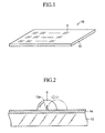
- FIG. 1 is an external view (a perspective view) illustrating the general construction of a DNA chip 10
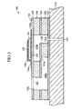
- FIG. 2 is an enlarged sectional view of the DNA chip shown in FIG. 1.
- the DNA chip 10 is constructed by arranging plural micro spots S, which are formed by micro drops of a sample solution, on a DNA chip substrate 12, which is made of microscope slide glass.
- a protrusion 12a is formed on the DNA chip 12 at a predetermined position where the corresponding micro spot S is to be formed.
- the protrusion 12a serves to compensate for the position deviation. Specifically, when a portion of the micro spot S is caught by the protrusion 12a (see a two-dot chain line), as shown in FIG. 2, the micro spot S is moved to the predetermined position by the surface tension of the micro spot S.
- sample support layer 14 which is a poly-L-lysine layer having a hydrophilic property, is formed on the surface of the DNA chip substrate 12.
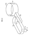
- FIG. 3 is an enlarged sectional view of the micropipette 100
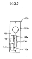
- FIG. 4 is a see-through perspective view illustrating the construction of a flow channel for a sample solution in the micropipette 100
- FIG. 5 is a plan view of the micropipette 100.
- the micropipette 100 includes a nozzle plate 110, a cavity unit 120 fixed to the upper surface of the nozzle plate 110, and an actuator unit 130 fixed to the upper surface of the cavity unit 120.
- a through-hole i.e., a nozzle 112 through which the sample solution passes.
- the nozzle plate 110 is formed from a thin ceramic plate.
- the material of the nozzle plate 110 includes, for example, zirconium oxide, aluminum oxide, magnesium oxide, aluminum nitride, and silicon nitride. Most preferably, a material mainly containing fully stabilized zirconium oxide or a material mainly containing partially stabilized zirconium oxide is used in terms of mechanical strength and a reaction to the material of a piezoelectric/electrostrictive film or an electrode film.
- the cavity unit 120 includes a connection plate 121, a flow channel plate 122, an orifice plate 123, a cavity plate 124, and an injection port plate 125.
- the connection plate 121, the flow channel plate 122, the orifice plate 123, the cavity plate 124, and the injection port plate 125 are formed from a thin ceramic plate.
- the connection plate 121, the flow channel plate 122, the orifice plate 123, the cavity plate 124, the injection port plate 125, and the nozzle plate 110 are sintered while they are stacked in order on the nozzle plate 110. As a result, they are integrally formed at the nozzle plate 110.
- connection plate 121 is disposed at the connection between the cavity plate 120 and the nozzle plate 110 such that the connection plate 121 is joined to the upper surface of the nozzle plate 110.
- connection plate 121 is formed a through-hole having the same diameter as the nozzle 112, i.e., a nozzle communication hole 121a.
- the nozzle communication hole 121a is connected to a cavity 124a formed in the cavity plate 124 via a sample outlet hole 126.
- the sample outlet hole 126 is a through-hole having a diameter greater than that of the nozzle communication hole 121 a.
- the sample outlet hole 126 is formed through the flow channel plate 122 and the orifice plate 123.
- a sample supply channel 122a In the flow channel plate 122 is formed a sample supply channel 122a, through which the sample solution is supplied to the cavity 124a.
- the sample supply channel 122a and the cavity 124a are connected with each other via an orifice 123a, which is a through-hole, having a small diameter, formed in the orifice plate 123.
- the injection port plate 125 is disposed at the uppermost layer of the cavity unit 120.
- a sample injection port 125a which is a through-hole for allowing the sample solution to be injected toward the sample supply channel 122a formed in the flow channel plate 122.
- the sample injection port 125a and the sample supply channel 122a formed in the flow channel plate 122 are connected with each other via a sample introduction hole 127, which is a through-hole.
- the sample introduction hole 127 is formed through the orifice plate 123 and the cavity plate 124.
- a sample solution flow channel is formed in the cavity unit 120 with the above-stated construction such that the sample solution flow channel extends from the sample injection port 125a to the nozzle 112.
- the dimension of the orifice 123a is set such that, when the cavity 124a is pressurized, the sample solution in the cavity 124a does not flow backward to the sample supply channel 122a through the small-diameter orifice 123a but flows out toward the nozzle 112 through the sample outlet hole 126, and therefore, micro drops of the sample solution are ejected to the outside from the nozzle 112.
- the actuator unit 130 includes a piezoelectric/electrostrictive layer 131, a lower electrode 132 fixed to the lower surface of the piezoelectric/electrostrictive layer 131, and an upper electrode 133 fixed to the upper surface of the piezoelectric/electrostrictive layer 131.
- the piezoelectric/electrostrictive layer 131 is disposed at a predetermined position corresponding to the cavity 124a (i.e., right above the cavity 124a).
- the lower electrode 132 is fixed to the upper surface of the injection port plate 125, and therefore, the actuator unit 130 is fixed to the upper surface of the cavity unit 120.
- the actuator unit 130 is constructed such that the actuator unit 130 changes the interior volume of the cavity 124a, when drive voltage is applied between the lower electrode 132 and the upper electrode 133, to eject a predetermined amount of the sample solution from the nozzle 112.
- the lower electrode 132 is connected to a lower electrode wiring pattern 132a, which is a conductive film formed at the upper surface of the injection port plate 125.
- the upper electrode 133 is connected to an upper electrode wiring pattern 133a, which is a conductive film formed at the upper surface of the injection port plate 125.
- a lower electrode input terminal 141 is formed at the upper surface of the injection port plate 125.
- the lower electrode input terminal 141 is connected to the lower electrode wiring pattern 132a.
- an upper electrode input terminal 142 is formed at the upper surface of the injection port plate 125.
- the upper electrode input terminal 142 is connected to the upper electrode wiring pattern 133a.
- the lower electrode input terminal 141 and the upper electrode input terminal 142 are connected to an external instrument that drives the actuator unit 130. Consequently, the actuator unit 130 is driven by drive voltage applied between the lower electrode input terminal 141 and the upper electrode input terminal 142 via the external instrument.
- FIGS. 6A and 6B illustrate the construction of the dispensing apparatus 200. Specifically, FIG. 6A is a plan view of the dispensing apparatus 200, and FIG. 6B is a side view of the dispensing apparatus 200. FIG. 7 is an exploded perspective view of the dispensing apparatus 200.
- the dispensing apparatus 200 includes a plurality (10 in the drawing) of micropipettes 100 arranged in two dimensions. All the micropipettes 100 have a common nozzle plate 110, the construction of which has already been described above.
- the common nozzle plate 110 is a ceramic plate.
- the dispensing apparatus 200 includes sample introduction members 210 for introducing the sample solution to the respective sample injection ports 125a of the micropipettes 110 (see FIG. 5). As shown in FIGS. 6A and 6B, the sample introduction members 210 are connected to the upper surfaces of the micropipettes 110 arranged in the two dimensions. As shown in FIG. 7, the sample introduction members 210 are fixed to the upper surface of the nozzle plate 110 by means of threaded holes 114 formed in the nozzle plate 110 and fixing bolts 212.
- sample injection channels 214 which are constructed in the shape of a through-hole, are formed in each sample introduction member 210.
- the openings at the lower ends of the sample injection channels 214 are connected to the corresponding sample injection ports 125a of the micropipettes 110 (see FIG. 5).
- the openings at the upper ends of the sample injection channels 214 are connected to the lower ends of introduction tubes 216, which are constructed in the shape of a trumpet whose diameter gradually increases upward.
- the plural introduction tubes 216 arranged in two dimensions are disposed and constructed such that the introduction tubes 216 are coupled with plural sample storage portions 222, which are formed at a cartridge 220 that stores a sample solution, while the sample storage portions 222 protrude downward from the cartridge 220.
- the cartridge 220 is formed by injection molding of a soft synthetic resin.
- the cartridge 220 is constructed such that openings are formed at the bottoms of the sample storage portions 222 using a needle, and therefore, the sample solution stored in the sample storage portions 222 is introduced into the introduction tubes 216, whereby different kinds of sample solutions are supplied to the respective sample injection ports 125a.
- FIG. 8 is a side view illustrating a flight state detection apparatus 300 mounted below the nozzle plate 110, having sample solution ejection ports, of the above-described dispensing apparatus 200.
- the DNA chip substrate 12 shown in FIG. 1 and the flight state detection apparatus 300 are disposed on an X-Y stage (not shown) such that the flight state detection apparatus 300 can be located below the nozzle plate 110 in a predetermined positional relationship when the X-Y stage is driven.
- the flight state detection apparatus 300 is constructed such that the flight state detection apparatus 300 can detect whether or not the sample solution is accurately ejected from the respective micropipettes 100 of the dispensing apparatus 200.
- the concrete construction of the flight state detection apparatus 300 according to the present invention will be described.
- FIG. 9A is an enlarged side sectional view of the flight state detection apparatus 300 according to the first embodiment.
- the flight state detection apparatus 300 includes a sensor substrate 310, a piezoelectric/electrostrictive element 320, and an aperture plate 330.
- the sensor substrate 310 is constructed from a plate-shaped member.
- the sensor substrate 310 is made of ceramic.
- fully stabilized or partially stabilized zirconia, alumina, magnesia, or silicon nitride may be used as the ceramic for the sensor substrate 310.
- the fully stabilized or partially stabilized zirconia can be used since the fully stabilized or partially stabilized zirconia has high tenacity and high mechanical strength, and furthermore, the fully stabilized or partially stabilized zirconia has small reaction to a piezoelectric/electrostrictive film forming the piezoelectric/electrostrictive element or the material of the electrode, although the fully stabilized or partially stabilized zirconia is constructed in the shape of a thin plate.
- the sensor substrate 310 includes a thick support part 311 and a vibrating plate (vibration generating part) 312.
- the thick support part 311 and the vibrating plate 312 are integrally formed to constitute a single body.
- the thick support part 311 has a thickness greater than the vibrating plate 312, which is formed from a plate-shaped member.
- the vibrating plate 312 is a plate-shaped member extending along the longitudinal direction (along the right-and-left direction in the drawing). The vibrating plate 312 is supported by the thick support part 311 in a cantilever shape.
- the piezoelectric/electrostrictive element 320 is attached to a detection part 312a, which is the fixed end of the vibrating plate 312.
- the piezoelectric/electrostrictive element 320 is fixedly attached to the inside surface 312b, which is the upper surface in the drawing, of the vibrating plate 312.
- the piezoelectric/electrostrictive element 320 is constructed such that the piezoelectric/electrostrictive element 320 can convert vibration generated at the cantilever-type vibrating plate 312 into an electric signal.
- the thickness of the piezoelectric/electrostrictive element 320 is relatively small as compared to the vibrating plate 312 (For convenience of the description, the thickness of the piezoelectric/electrostrictive element 320 is exaggeratedly shown in FIG. 9A. The same conditions will be applied to the following drawings, i.e., FIGS. 10 to 22).
- a coating layer 313 is formed on the inside surface 312b of a target part 312c, which is the free end of the vibrating plate 312 (one end of the vibrating plate in the longitudinal direction).
- the coating layer 313 is constructed from a thin film made of a material having a low affinity (wettability) for micro drops of the sample solution.
- a water-repellent material a fluorine-based synthetic resin
- the aperture plate 330 is disposed on the sensor substrate 310 such that the aperture plate 330 is opposite to the inside surface 312b of the vibrating plate 312.
- an aperture 331 is formed which is a through-hole for allowing the micro drops to pass therethrough.
- the aperture plate 330 is disposed such that the aperture 331 is opposite to the nozzle 112 (see FIG. 3) formed at the nozzle plate 110 (see FIG. 8) of the micropipette 100.
- FIG. 9B is a plan view of the flight state detection apparatus 300 (a view illustrating the flight state detection apparatus 300 shown in FIG. 8 when seen from the nozzle plate 110 side of the micropipette 100).
- FIG. 9C is a plan view of the flight state detection apparatus 300 with the aperture plate 330 being removed.
- the aperture 331 is located such that the aperture 331 is opposite to the coating layer 313 formed at the target part 312c. Also, as shown in FIG. 9A, the aperture 331 is located at a higher position than the coating layer 313 formed at the target part 312c, i.e., at the upper stream side in the flight direction D of the micro drops.
- the flight state detection apparatus 300 is constructed such that the micro drops which are flying along a predetermined flight route in the flight direction D can pass through the aperture 331 to collide with the target part 312c (the coating layer 313), and vibration generated in the vibrating plate 312 due to the collision can be converted into an electric signal by the piezoelectric/electrostrictive element 320.
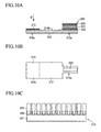
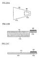
- FIG. 10A is an enlarged sectional view of the vibrating plate 312 and its surroundings.
- the piezoelectric/electrostrictive element 320 includes a piezoelectric/electrostrictive layer 321, a lower electrode 322 formed at one-side surface of the piezoelectric/electrostrictive layer 321, and an upper electrode 323 formed at the other-side surface of the piezoelectric/electrostrictive layer 321.
- the piezoelectric/electrostrictive layer 321 is constructed from a thin plate having a piezoelectric effect and a converse piezoelectric effect, for example, a thin plate made of a piezoelectric/electrostrictive material (PZT or the like).
- the lower electrode 322 and the upper electrode 323 are constructed from a metal film.
- FIG. 10B is an enlarged plan view of the vibrating plate 312 and its surroundings.
- the detection part 312a of the vibrating plate 312 has a smaller width than that of the other part of the vibrating plate 312.
- the plane shape of the vibrating plate 312 is set such that, when the micro drops of the sample solution fly from above (from above in the FIG. 10A) to collide with the target part 312c (the coating layer 313), and therefore, vibration is generated in the vibrating plate 312, stress is concentrated on the detection part 312a, and large voltage is generated in the piezoelectric/electrostrictive element 320 due to the stress concentration.
- FIG. 10C is a plan view of the sensor substrate 310. As shown in FIG. 10C, plural vibrating plates 312 are formed at the sensor substrate 310 such that the vibrating plates 312 extend from the thick support part 311 approximately in the horizontal direction.
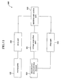
- the control circuit 340 includes a voltage acquisition part 341 for acquiring the voltage generated in the piezoelectric/electrostrictive element 320, a drive part 342 for applying a drive voltage to the piezoelectric/electrostrictive element 320, an operation and control part 343 connected to the voltage acquisition part 341 and the drive part 342, and a drive part 344 for applying a drive voltage to the respective micropipettes 100.
- the voltage acquisition part 341 is electrically connected to the piezoelectric/electrostrictive element 320 for acquiring an electromotive force generated in the piezoelectric/electrostrictive element 320 when the micro drops of the sample solution collide with the target part 312c (see FIG. 10A).
- the drive part 342 is electrically connected to the piezoelectric/electrostrictive element 320 for applying a drive voltage to the piezoelectric/electrostrictive element 320, such that the piezoelectric/electrostrictive element 320 can be driven, to forcibly vibrate the vibrating plate 312 (see FIGS. 10A to 10C).
- the drive part 342 is constructed such that a voltage having an arbitrary waveform (including a direct current, and also including various waveforms, such as a sine waveform, a rectangular waveform, a pulse waveform, etc., in an alternating current) can be applied to the piezoelectric/electrostrictive element 320 under the control of the operation and control part 343.
- a voltage having an arbitrary waveform including a direct current, and also including various waveforms, such as a sine waveform, a rectangular waveform, a pulse waveform, etc., in an alternating current
- the operation and control part 343 is constructed such that the operation and control part 343 receives a signal from the voltage acquisition part 341 and properly operates the received signal to detect the vibration state (including the magnitude of the vibration, the vibration mode, and the resonant frequency) of the vibrating plate 312 (see FIGS. 10A to 10C). Also, the operation and control part 343 is constructed such that the operation and control part 343 applies a drive signal to the drive part 342 to control the driving of the piezoelectric/electrostrictive element 320. Furthermore, the operation and control part 343 is connected to the respective micropipettes 100 via the drive part 344 for controlling the ejection of the sample solution from the respective micropipettes 100.
- the manufacturing process includes a pre-treatment process of forming a sample support layer 14 (see FIG. 2), which is a poly-L-lysine layer, on the surface of the DNA chip substrate 12, a sample manufacturing process of manufacturing a sample solution containing DNA pieces, and a supply process of supplying the manufactured sample solution onto the DNA chip substrate 12.
- the pre-treatment process is carried out as follows. First, the DNA chip substrate 12 is soaked in a predetermined alkali solution at the room temperature for at least two hours.
- a predetermined alkali solution for example, there may be used a solution obtained by dissolving NaOH in distilled water, adding ethanol in the mixture, and stirring the mixture until the mixture becomes fully transparent. After that, the DNA chip substrate 12 is taken out of the alkali solution, and is then washed in distilled water. Subsequently, the DNA chip substrate 12 is soaked in a poly-L-lysine solution manufactured by adding poly-L-lysine in distilled water for approximately one hour.
- the DNA chip substrate 12 is taken out of the poly-L-lysine solution, and the poly-L-lysine solution remaining on the DNA chip substrate 12 is removed by centrifugal separation. Subsequently, the DNA chip substrate 12 is dried at 40°C for approximately 5 minutes. In this way, a DNA chip substrate 12 having the poly-L-lysine sample support layer 14 formed on the surface thereof is obtained.
- the sample manufacturing process includes an amplifying process of amplifying the base sequence of the DNA pieces, using polymerase chain reaction (PCR), to obtain a PCR product, a powder producing process of drying the obtained PCR product to obtain DNA powder, and a mixing process of dissolving the obtained DNA powder in a buffer solution.
- PCR polymerase chain reaction
- a Tris-EDTA (TE) buffer solution is added to the DNA powder, and the mixture is left for a few hours until the DNA powder is fully dissolved in the buffer solution. As a result, a sample solution is prepared.
- the concentration of the sample solution prepared at this step is 1 to 10 ⁇ g/ ⁇ l
- the sample solution obtained as described above is stored in the sample storage portions 222 of the cartridge 220 shown in FIG. 7. Since the cartridge 220 is mounted to the dispensing apparatus 200 shown in FIG. 6, the sample solution is supplied into the respective micropipettes 100 in the dispensing apparatus 200. And the micro drops of the sample solution are ejected toward the DNA chip substrate 12 (see FIG. 1) from the respective micropipettes 100, and therefore, the micro drops of the sample solution are supplied onto the DNA chip substrate 12. As a result, plural micro spots S of the sample solution are formed on the DNA chip substrate 12 in a predetermined array. In this way, the DNA chip 10 is manufactured.
- the determination as to whether or not the micro drops of the sample solution are properly formed on the DNA chip substrate 12 in the predetermined array cannot be performed with the naked eye.
- the construction of an apparatus for determining whether the ejecting operation is not correctly carried out in the respective micropipettes 100 by scanning the laser beam as described above is very expensive.
- the determination as to whether the ejecting operation is not correctly carried out in the respective micropipettes 100 of the dispensing apparatus 200 is accomplished using the flight state detection apparatus 300 according to the preferred embodiment of the present invention as shown in FIG. 8.
- the construction of the flight state detection apparatus 300 is very simple, and therefore, the manufacturing costs of the flight state detection apparatus 300 are very low.
- the construction of the flight state detection apparatus 300 is very simple as described above, it is possible for the flight state detection apparatus 300 to accurately perform the determination as to whether the ejecting operation is not correctly carried out.
- FIGS. 12A and 12B illustrate the vibration state of the vibrating plate 312 (see FIGS. 9A to 9C and 10A to 10C).
- the flight state detection apparatus 300 is disposed below the nozzle plate 110 of the micropipettes 100.
- the driving operation of the dispensing apparatus 200 is controlled by the operation and control part 343 and drive part 344 as shown in FIG. 11. Specifically, under the control of the operation and control part 343, a drive voltage from the drive part 344 is applied to the actuator units 130 (see FIG. 5) of the respective micropipettes 100 mounted in the dispensing apparatus 200, whereby the respective micropipettes 100 are driven. As a result, micro drops of the sample solution are ejected to the flight state detection apparatus 300 from the respective micropipettes 100.
- the micro drops of the sample solution are ejected as described above, the micro drops pass through the aperture 331, and then collide with the target part 312c (the coating layer 313) of the vibrating plate 312 in regular sequence.
- the vibrating plate 312 is vibrated by this collision.
- an electromotive force is generated in the piezoelectric/electrostrictive element 320. That is to say, voltage is generated between the lower electrode 322 and the upper electrode 323 shown in FIGS. 10A to 10C depending upon the vibration state of the vibrating plate 312.
- the vibrating plate 312 is vibrated such that the vibrating plate 312 is bent (a primary bending mode).
- stress is generated in the detection part 312a.
- the generated stress is converted into an electromotive force by the piezoelectric/electrostrictive element 320 (see FIGS. 10A to 10C).
- the vibrating plate 312 is vibrated such that the vibrating plate 312 is twisted (a twisting mode).
- stress which is smaller than the stress generated in the bending mode as shown in FIG. 12A, is generated in the detection part 312a. Consequently, an electromotive force, which is smaller than the electromotive force generated in the bending mode, is generated in the piezoelectric/electrostrictive element 320 (see FIGS. 10A to 10C).
- the micro drops do not pass through the aperture 331 but collide with the upper surface of the aperture plate 330. In this case, the micro drops do not collide with the target part 312c, and therefore, no vibration is generated in the vibrating plate 312 (or the amplitude of the vibrating plate is converged toward zero).
- the voltage generated in the piezoelectric/electrostrictive element 320 is acquired by the voltage acquisition part 341, and the electromotive force acquired by the voltage acquisition part 341 is operated by the operation and control part 343, whereby the vibration state of the vibrating plate 312 is detected.
- the operation and control part 343 drives the micropipettes 100 at a specific frequency f1 satisfying the following inequality: n - 0.2 f 1 ⁇ f 0 ⁇ n + 0.25 f 1 n is a natural number .
- the micro drops of the sample solution are ejected one by one for a period T corresponding to the specific frequency f1.
- the driving operation of the micropipettes 100 is controlled such that the ejection of the micro drops is carried out in the condition satisfying the following inequality: T 1 ⁇ 0.2 T 0.
- the vibrating plate 312 is vibrated at a frequency approximately equal to the resonant frequency of the vibrating plate 312. And the micro drops collide with the target part 312c one by one while the micro drops are synchronized with the vibration of the vibrating plate 312. Consequently, the vibration of the vibrating plate 312 is effectively prevented from being varied due to the collision between the micro drops and the vibrating plate 312.
- the detection part 312a of the vibrating plate 312 has a smaller width than that of the other part of the vibrating plate 312. Consequently, when the micro drops of the sample solution fall from above to collide with the target part 312c, and therefore, vibration is generated in the vibrating plate 312, stress is concentrated on the detection part 312a. Due to the stress concentration, large voltage is generated in the piezoelectric/electrostrictive element 320.
- most spray of the sample solution which is generated when the micro drops of the sample solution collide with the coating layer 313, is not attached to the surface of the coating layer 313 for a long time but drops due to gravity.
- most of the sample solution is removed from the inside surface 312b of the vibrating plate 312.
- some of the spray may not be completely removed from the inside surface 312b of the vibrating plate 312. In other words, some of the spray may be left on the inside surface 312b of the vibrating plate 312.
- the remaining spray may be removed from the inside surface 312b of the vibrating plate 312 by forcibly vibrating the vibration plate 312 from the outside as will be described below.
- the drive part 342 applies a drive voltage having the above-described resonant frequency f0 to the piezoelectric/electrostrictive element 320 under the control of the operation and control part 343.
- the piezoelectric/electrostrictive element 320 is driven, and the vibrating plate 312 (see FIGS. 9A to 9C) is forcibly vibrated. Consequently, the spray of the sample solution is removed from the vibrating plate 312.
- the vibrating plate 312 is forcibly vibrated, a very small amount of the sample solution may be left and solidified on the vibrating plate 312. As a result, the resonant frequency of the vibrating plate 312 is changed.
- the drive part 342 applies a DC voltage to the piezoelectric/electrostrictive element 320 for a predetermined period of time (a time sufficiently longer than a period corresponding to the expected resonant frequency) under the control of the operation and control part 343, and then the application of the DC voltage is interrupted.
- a predetermined period of time a time sufficiently longer than a period corresponding to the expected resonant frequency
- an AC voltage is generated in the piezoelectric/electrostrictive element 320. Consequently, a voltage waveform is generated in the piezoelectric/electrostrictive element 320.
- the voltage waveform is acquired by the operation and control part 343 through the voltage acquisition part 341.
- the operation and control part 343 can acquire the changed resonant frequency by acquiring the frequency of the voltage waveform.
- the acquired new resonant frequency is used for the drive part 342 to drive the piezoelectric/electrostrictive element 320.
- FIGS. 13A and 13B a second embodiment of the flight state detection apparatus according to the present invention will be described in detail with reference to FIGS. 13A and 13B.
- the components of the flight state detection apparatus according to the second embodiment identical in operation and function to those of the flight state detection apparatus according to the above-described first embodiment are omitted from the drawings.
- the components of the flight state detection apparatus according to the second embodiment identical in operation and function to those of the flight state detection apparatus according to the first embodiment are denoted by the same reference numerals as those of the first embodiment.
- the description of the first embodiment will be quoted with respect to the second embodiment (The same conditions will be applied to the following other embodiments and modifications).
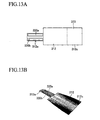
- FIG. 13A is an enlarged plan view of the vibrating plate 312 according to the second embodiment and its surroundings
- FIG. 13B is an enlarged plan view illustrating the vibration state of the vibrating plate 312.
- two piezoelectric/electrostrictive elements 320a and 320b are mounted at the detection part 312a of the vibrating plate 312.
- the piezoelectric/electrostrictive elements 320a and 320b are electrically connected to the operation and control part 343 (see FIG. 11), respectively.
- the two piezoelectric/electrostrictive elements 320a and 320b have the same construction of the piezoelectric/electrostrictive element 320 shown in FIG. 10A.
- the polarizing directions of piezoelectric/electrostrictive layers of the piezoelectric/electrostrictive elements 320a and 320b are the same.
- phase difference is generated by a half period between the output voltage waveform of the piezoelectric/electrostrictive element 320a and the output voltage waveform of the piezoelectric/electrostrictive element 320b.
- bending-mode vibration is generated in the vibrating plate 312
- no phase difference is generated between the output voltage waveform of the piezoelectric/electrostrictive element 320a and the output voltage waveform of the piezoelectric/electrostrictive element 320b.
- the vibration mode generated in the vibrating plate 312 is determined by the comparison between the output voltage waveform of the piezoelectric/electrostrictive element 320a and the output voltage waveform of the piezoelectric/electrostrictive element 320b. In this way, the collision state between the micro drops and the target part 312c of the vibrating plate 312, i.e., the flight state of the micro drops is determined.
- two piezoelectric/electrostrictive elements 320a and 320b are mounted at a single vibrating plate 312.
- One of the piezoelectric/electrostrictive elements i.e., the piezoelectric/electrostrictive element 320a, is connected to the drive part 342.
- the other piezoelectric/electrostrictive element 320b is connected to the voltage acquisition part 341.
- the drive part 342 is constructed such that a voltage having an arbitrary waveform (including a direct current, and also including various waveforms, such as a sine waveform, a rectangular waveform, a pulse waveform, etc., in an alternating current) can be applied to the piezoelectric/electrostrictive element 320a under the control of the operation and control part 343 (see FIG. 11) (The same conditions will be applied to the drive part 342 shown in FIGS. 14B, 14C, and 15A to 15C, which will be described below).
- a voltage having an arbitrary waveform including a direct current, and also including various waveforms, such as a sine waveform, a rectangular waveform, a pulse waveform, etc., in an alternating current
- a DC voltage to the piezoelectric/electrostrictive element 320a is applied by the drive part 342 for a predetermined period of time (time sufficiently longer than a period corresponding to the expected resonant frequency), and then the application of the DC voltage is interrupted.
- a vibration system including the vibration plate 312, the piezoelectric/electrostrictive element 320a, and the piezoelectric/electrostrictive element 320b. Due to this free vibration with damping, an AC voltage is generated in the piezoelectric/electrostrictive element 320b.
- a voltage waveform is generated in the piezoelectric/electrostrictive element 320b, and the resonant frequency of the vibrating plate 312 is acquired based on the voltage waveform generated in the piezoelectric/electrostrictive element 320b.
- the acquired new resonant frequency is used for the drive part 342 to drive the piezoelectric/electrostrictive element 320.
- the AC voltage is applied to one of the piezoelectric/electrostrictive elements, i.e., the piezoelectric/electrostrictive element 320a, from the drive part 342, and the waveform of the electromotive force generated in the other piezoelectric/electrostrictive element 320b is acquired by the voltage acquisition part 341. Consequently, it is possible to acquire the resonant frequency of the vibrating plate 312 for a short period of time.
- the drive part 342 outputs the AC voltage having a waveform allowing the frequency to be changed as time passes.
- the frequency in the case that the voltage acquired by the voltage acquisition part 341 is the maximum or in the case that the impedance or the phase is sharply changed may be chosen as the acquired value of the resonant frequency.
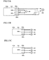
- piezoelectric/electrostrictive elements 320a to 320d are mounted at a single vibrating plate 312.
- the piezoelectric/electrostrictive element 320a and the piezoelectric/electrostrictive element 320d are symmetrically disposed along the lateral direction of the vibrating plate 312 about a middle line C of the vibrating plate 312 located between the piezoelectric/electrostrictive element 320a and the piezoelectric/electrostrictive element 320d.
- the piezoelectric/electrostrictive element 320b and the piezoelectric/electrostrictive element 320c are symmetrically disposed along the lateral direction of the vibrating plate 312 about the middle line C of the vibrating plate 312.
- the piezoelectric/electrostrictive element 320a and the piezoelectric/electrostrictive element 320b are connected to the drive part 342.
- the piezoelectric/electrostrictive element 320c and the piezoelectric/electrostrictive element 320d are connected to the voltage acquisition part 341.
- three piezoelectric/electrostrictive elements 320a to 320c are mounted at a single vibrating plate 312.
- the piezoelectric/electrostrictive element 320a and the piezoelectric/electrostrictive element 320c are symmetrically disposed along the lateral direction of the vibrating plate 312 about a middle line C of the vibrating plate 312 located between the piezoelectric/electrostrictive element 320a and the piezoelectric/electrostrictive element 320c.
- the piezoelectric/electrostrictive element 320b is disposed on the middle line C of the vibrating plate 312.
- the piezoelectric/electrostrictive element 320a is connected to the drive part 342.
- the piezoelectric/electrostrictive element 320b and the piezoelectric/electrostrictive element 320c are connected to the voltage acquisition part 341.
- the acquisition of the resonant frequency through the application of the DC voltage, the acquisition of the resonant frequency through the application of the AC voltage, and the determination of the twisting mode are carried out.
- the detection of the bending mode is carried out by the output of the piezoelectric/electrostrictive element 320b, and the detection of the twisting mode is carried out by the output of the piezoelectric/electrostrictive element 320c. Consequently, it is possible to precisely carry out the determination of the vibration state of the vibrating plate 312.
- the ratio of the resonant frequency in the bending mode and the twisting mode can be obtained through an experiment or a computer simulation such as a finite element method, and therefore, it is possible to calculate the resonant frequency of the bending mode from the resonant frequency of the twisting mode. Consequently, it is possible to detect the flight state of the micro drops using both the bending mode and the twisting mode.
- piezoelectric/electrostrictive elements 320a to 320d are mounted at a single vibrating plate 312.
- the piezoelectric/electrostrictive element 320a and the piezoelectric/electrostrictive element 320d which are symmetrically disposed along the lateral direction of the vibrating plate 312, are connected to the drive part 342.
- the piezoelectric/electrostrictive element 320b and the piezoelectric/electrostrictive element 320c which are symmetrically disposed along the lateral direction of the vibrating plate 312, are connected to the voltage acquisition part 341.
- three piezoelectric/electrostrictive elements 320a to 320c are mounted at a single vibrating plate 312.
- the piezoelectric/electrostrictive element 320a and the piezoelectric/electrostrictive element 320c which are symmetrically disposed along the lateral direction of the vibrating plate 312, are connected to the drive part 342.
- the piezoelectric/electrostrictive element 320b which is disposed at the middle of the vibrating plate 312 along the lateral direction of the vibrating plate 312, is connected to the voltage acquisition part 341.
- three piezoelectric/electrostrictive elements 320a to 320c are mounted at a single vibrating plate 312.
- the piezoelectric/electrostrictive element 320a and the piezoelectric/electrostrictive element 320c which are symmetrically disposed along the lateral direction of the vibrating plate 312, are connected to the voltage acquisition part 341.
- the piezoelectric/electrostrictive element 320b which is disposed at the middle of the vibrating plate 312 along the lateral direction of the vibrating plate 312, is connected to the drive part 342.
- the voltage application or the electromotive measurement can be carried out with respect to the piezoelectric/electrostrictive elements symmetrically disposed along the lateral direction of the vibrating plate 312. Furthermore, in all cases, the respective piezoelectric/electrostrictive elements 320a, 320b... are disposed on the one-side surface of the vibrating plate 312 such that the directions of the piezoelectric/electrostrictive layers are the same.
- the polarizing directions of the piezoelectric/electrostrictive layers of the two piezoelectric/electrostrictive elements are the same, the lower electrodes of the two piezoelectric/electrostrictive elements are grounded together, and AC voltages having the same phase are applied to the upper electrodes of the two piezoelectric/electrostrictive elements, whereby the vibration of the primary bending mode can be generated in the vibrating plate 312.
- the polarizing directions of the piezoelectric/electrostrictive layers of the two piezoelectric/electrostrictive elements are the same, the lower electrode of one of the piezoelectric/electrostrictive elements and the upper electrode of the other piezoelectric/electrostrictive element are grounded, and AC voltages having the same phase are applied to the remaining electrodes, whereby the vibration of the twisting mode can be generated in the vibrating plate 312.
- the polarizing directions of the piezoelectric/electrostrictive layers of the two piezoelectric/electrostrictive elements are the same, the lower electrode of one of the piezoelectric/electrostrictive elements and the upper electrode of the other piezoelectric/electrostrictive element are grounded, and the electromotive force between the remaining electrodes of the two piezoelectric/electrostrictive elements is measured, whereby the resonant frequency of the vibration of the primary bending mode in the vibrating plate 312 can be acquired.
- the polarizing directions of the piezoelectric/electrostrictive layers of the two piezoelectric/electrostrictive elements are the same, the lower electrodes of the two piezoelectric/electrostrictive elements are connected to each other, and the electromotive force between the upper electrodes of the two piezoelectric/electrostrictive elements is measured, whereby the resonant frequency of the vibration of the twisting mode in the vibrating plate 312 can be acquired.
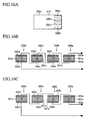
- FiG. 16A is a plan view illustrating the construction of this embodiment.
- FIGS. 16B and 16C are views illustrating the electrical connection of the piezoelectric/electrostrictive elements according to this embodiment.
- piezoelectric/electrostrictive elements 320a to 320d are mounted at a single vibrating plate 312 such that the piezoelectric/electrostrictive elements 320a to 320d are symmetrically disposed along the lateral direction of the vibrating plate 312.
- the piezoelectric/electrostrictive elements 320a to 320d may be connected to each other, for example, as shown in FIG. 16B or 16C.
- connection state shown in FIG. 16B is as follows.
- a lower electrode 322a of the piezoelectric/electrostrictive element 320a and an upper electrode 323b of the piezoelectric/electrostrictive element 320b are connected with each other.
- a lower electrode 322b of the piezoelectric/electrostrictive element 320b and an upper electrode 323c of the piezoelectric/electrostrictive element 320c are connected with each other.
- a lower electrode 322c of the piezoelectric/electrostrictive element 320c and an upper electrode 323d of the piezoelectric/electrostrictive element 320d are connected with each other.
- the connection state shown in FIG. 16C is as follows.
- An upper electrode 323a of the piezoelectric/electrostrictive element 320a and a lower electrode 322b of the piezoelectric/electrostrictive element 320b are connected with each other.
- a lower electrode 323d of the piezoelectric/electrostrictive element 320d and a lower electrode 322c of the piezoelectric/electrostrictive element 320c are connected with each other. That is to say, the piezoelectric/electrostrictive element 320a and the piezoelectric/electrostrictive element 320b are electrically connected with each other.
- the piezoelectric/electrostrictive element 320c and the piezoelectric/electrostrictive element 320d are electrically connected with each other.
- the one-side output terminal of the electrically connected piezoelectric/electrostrictive elements 320a and 320b is constructed from the upper electrode 323b of the piezoelectric/electrostrictive element 320b, and the other-side output terminal of the electrically connected piezoelectric/electrostrictive elements 320a and 320b is constructed from the lower electrode 322a of the piezoelectric/electrostrictive element 320a.
- the one-side output terminal of the electrically connected piezoelectric/electrostrictive elements 320c and 320d is constructed from the upper electrode 323c of the piezoelectric/electrostrictive element 320c
- the other-side output terminal of the electrically connected piezoelectric/electrostrictive elements 320c and 320d is constructed from the lower electrode 322d of the piezoelectric/electrostrictive element 320d.
- the one-side output terminals are short-circuited with each other, and an output voltage corresponding to the vibration state is generated between the other-side output terminals.
- the electromotive force generated in the piezoelectric/electrostrictive elements 320a and 320d which are located at opposite ends of the vibrating plate 312 in the lateral direction of the vibrating plate 312, is greater than the electromotive force generated in the piezoelectric/electrostrictive elements 320b and 320c, which are located closer to the middle of the vibrating plate 312 in the lateral direction of the vibrating plate 312.
- electromotive forces ⁇ V1 having the same absolute value and half-wavelength deviated phases are generated in the piezoelectric/electrostrictive elements 320a and 320d, which are symmetrically disposed in the lateral direction of the vibrating plate 312, due to the vibration of the twisting mode in the vibrating plate 312.
- electromotive forces ⁇ 0.5V1 having the same absolute value and half-wavelength deviated phases are generated in the piezoelectric/electrostrictive elements 320b and 320c, which are symmetrically disposed in the lateral direction of the vibrating plate 312, due to the vibration of the twisting mode in the vibrating plate 312.
- the total output voltage becomes zero. That is to say, in the case that the vibration of the complete twisting mode is generated in the vibrating plate 312, the output voltage of the circuit shown in FIG. 16B becomes zero.
- an electromotive force of 2V1 is generated between the upper electrode 323b and the lower electrode 322a, i.e., the output terminals of the piezoelectric/electrostrictive elements 320a and 320b, which are electrically connected with each other, due to the vibration of the primary bending mode in the vibrating plate 312.
- an electromotive force of 2V1 is generated between the upper electrode 323c and the lower electrode 322d, i.e., the output terminals of the piezoelectric/electrostrictive elements 320c and 320d, which are electrically connected with each other.
- the upper electrode 323b and the upper electrode 323c are short-circuited with each other. Consequently, in the case that the vibration of the complete primary bending mode is generated in the vibrating plate 312, the output voltage of the circuit shown in FIG. 16C becomes zero.
- an electromotive force of +1.5V1 is generated between the upper electrode 323b and the lower electrode 322a, i.e., the output terminals of the piezoelectric/electrostrictive elements 320a and 320b, due to the vibration of the twisting mode in the vibrating plate 312.
- an electromotive force of -1.5V1 is generated between the upper electrode 323c and the lower electrode 322d, i.e., the output terminals of the piezoelectric/electrostrictive elements 320c and 320d. Consequently, in the case that the vibration of the complete twisting mode is generated in the vibrating plate 312, the output voltage of the circuit shown in FIG. 16C becomes 3V1.
- the detection of the flight state of the micro drops can be performed with higher sensitivity, and the determination of the vibration mode can be more easily performed by disposing the plural piezoelectric/electrostrictive elements 320a, 320b... on the vibrating plate 312, and properly setting the electrical connection state therebetween.
- the plural piezoelectric/electrostrictive elements 320a, 320b... are electrically connected in series (not via the operation and control part 343 shown in FIG. 11), as such the circuits shown in FIGS. 16B and 16C are constructed. Consequently, according to this embodiment, the inner circuit construction of the operation and control part 343 shown in FIG. 11 is simplified, and therefore, the signal process performed by the operation and control part 343 is simplified.
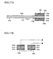
- FIG. 17A is an enlarged side sectional view illustrating the construction of this embodiment.
- FIG. 17B is a view illustrating the electrical connection of the piezoelectric/electrostrictive elements according to this embodiment.
- the piezoelectric/electrostrictive element 320a is mounted on the inside surface 312b of the detection part 312a of the vibrating plate 312.
- the piezoelectric/electrostrictive element 320b is mounted on the outside surface 312d of the detection part 312a of the vibrating plate 312. That is to say, the piezoelectric/electrostrictive elements 320a and 320b are disposed on the opposite-side surfaces of the vibrating plate 312, respectively.
- the lower electrode 322b of the piezoelectric/electrostrictive element 320b disposed on the outside surface 312d of the vibrating plate 312 is the electrode disposed adjacent to the vibrating plate 312.
- the lower electrode 322a of the piezoelectric/electrostrictive element 320a and the lower electrode 322b of the piezoelectric/electrostrictive element 320b are short-circuited with each other.
- an output voltage corresponding to the vibration state is generated between the upper electrode 323a of the piezoelectric/electrostrictive element 320a and the upper electrode 323b of the piezoelectric/electrostrictive element 320b.
- a tensile stress is generated in the piezoelectric/electrostrictive layer 321 a of the piezoelectric/electrostrictive element 320a
- a compressive stress is generated in the piezoelectric/electrostrictive layer 321 b of the piezoelectric/electrostrictive element 320b.
- FIG. 18A is an enlarged side sectional view illustrating the construction of this embodiment.
- FIG. 18B is a view illustrating the electrical connection of the piezoelectric/electrostrictive elements according to this embodiment.
- the piezoelectric/electrostrictive element 320a is mounted on the inside surface 312b of the detection part 312a of the vibrating plate 312. Also, the piezoelectric/electrostrictive element 320b is disposed above the piezoelectric/electrostrictive element 320a while an insulation layer 324 is interposed between the piezoelectric/electrostrictive elements 320a and 320b.
- the piezoelectric/electrostrictive element 320a, the insulation layer 324, and the piezoelectric/electrostrictive element 320b are integrally formed to constitute a single body by sintering.
- the piezoelectric/electrostrictive elements 320a and 320b are constructed such that the polarizing direction of the piezoelectric/electrostrictive layer 321a of the piezoelectric/electrostrictive element 320a is opposite to the polarizing direction of the piezoelectric/electrostrictive layer 321 b of the piezoelectric/electrostrictive element 320b.
- the lower electrode 322a of the piezoelectric/electrostrictive element 320a and the lower electrode 322b of the piezoelectric/electrostrictive element 320b are short-circuited with each other.
- the piezoelectric/electrostrictive element 320a and the upper electrode 323b of the piezoelectric/electrostrictive element 320b are electrically connected with each other.
- the output of the circuit shown in FIG. 18B is double the output for the case that only the piezoelectric/electrostrictive element 320a is provided (the case that the piezoelectric/electrostrictive element 320b is not provided). Consequently, even when super micro drops collide with the target part 312c, it is possible to detect the collision with high sensitivity.
- the flight state detection apparatus and the flight state detection method according to the present invention can detect the flight state of the micro object colliding with the target part only by disposing the target part on the flight route of the micro object in flight and detecting the collision state between the micro object and the target part using the piezoelectric/electrostrictive element. That is to say, according to the present invention, it is possible to accurately detect the flight state of the micro object ejected from the micro object ejection apparatus (the ejection state of the micro object ejection apparatus) through the use of the flight state detection apparatus, which is manufactured in a simplified structure and at low costs.
Landscapes
- Physics & Mathematics (AREA)
- General Physics & Mathematics (AREA)
- General Health & Medical Sciences (AREA)
- Chemical & Material Sciences (AREA)
- Analytical Chemistry (AREA)
- Biochemistry (AREA)
- Life Sciences & Earth Sciences (AREA)
- Health & Medical Sciences (AREA)
- Immunology (AREA)
- Pathology (AREA)
- Acoustics & Sound (AREA)
- Micromachines (AREA)
- Investigating Or Analyzing Materials By The Use Of Ultrasonic Waves (AREA)
- Automatic Analysis And Handling Materials Therefor (AREA)
Applications Claiming Priority (1)
| Application Number | Priority Date | Filing Date | Title |
|---|---|---|---|
| JP2005159799A JP4497370B2 (ja) | 2005-05-31 | 2005-05-31 | 微小物体の飛翔状態検出装置、及び微小物体の飛翔状態検出方法 |
Publications (3)
| Publication Number | Publication Date |
|---|---|
| EP1729124A2 true EP1729124A2 (de) | 2006-12-06 |
| EP1729124A3 EP1729124A3 (de) | 2009-04-15 |
| EP1729124B1 EP1729124B1 (de) | 2012-07-11 |
Family
ID=36939166
Family Applications (1)
| Application Number | Title | Priority Date | Filing Date |
|---|---|---|---|
| EP06252774A Expired - Lifetime EP1729124B1 (de) | 2005-05-31 | 2006-05-30 | Vorrichtung und Verfahren zur Erfassung der Fluglage eines Mikroobjekts |
Country Status (3)
| Country | Link |
|---|---|
| US (1) | US7615911B2 (de) |
| EP (1) | EP1729124B1 (de) |
| JP (1) | JP4497370B2 (de) |
Families Citing this family (3)
| Publication number | Priority date | Publication date | Assignee | Title |
|---|---|---|---|---|
| US20090151991A1 (en) * | 2007-12-14 | 2009-06-18 | Epson Imaging Devices Corporation | Mounting structure, electrooptic device, and electronic apparatus |
| EP3715826B1 (de) * | 2019-03-26 | 2024-03-06 | Infineon Technologies AG | Sensorvorrichtung, partikelsensorvorrichtung und verfahren zur detektion der dichte eines partikelförmigen materials |
| JP7426071B2 (ja) * | 2019-12-18 | 2024-02-01 | 国立研究開発法人産業技術総合研究所 | 気泡検出装置、気泡検出方法およびそのプログラム |
Citations (3)
| Publication number | Priority date | Publication date | Assignee | Title |
|---|---|---|---|---|
| JP2000180250A (ja) | 1998-10-09 | 2000-06-30 | Ngk Insulators Ltd | 質量センサ及び質量検出方法 |
| JP2001124789A (ja) | 1999-10-22 | 2001-05-11 | Ngk Insulators Ltd | マイクロピペット及び分注装置 |
| JP2001186881A (ja) | 1999-10-22 | 2001-07-10 | Ngk Insulators Ltd | Dnaチップの製造方法 |
Family Cites Families (16)
| Publication number | Priority date | Publication date | Assignee | Title |
|---|---|---|---|---|
| US4193010A (en) * | 1976-12-09 | 1980-03-11 | Essex Transducers Corporation | Sensor device using piezoelectric coating subjected to bending |
| US4131815A (en) * | 1977-02-23 | 1978-12-26 | Oceanography International Corporation | Solid piezoelectric sand detection probes |
| US4114063A (en) * | 1977-04-27 | 1978-09-12 | Westinghouse Electric Corp. | Piezoelectric sediment particle transport detector |
| US4540981A (en) * | 1981-10-29 | 1985-09-10 | Edo Western Corporation | Method and apparatus for detecting the presence of liquid |
| US4835435A (en) * | 1988-01-19 | 1989-05-30 | Hewlett-Packard Company | Simple, sensitive, frequency-tuned drop detector |
| US4904894A (en) * | 1989-01-24 | 1990-02-27 | Pennwalt Corporation | Hail sensor |
| US4976156A (en) * | 1989-10-30 | 1990-12-11 | Lew Hyok S | Impulse sensor with balanced mass-stiffness distribution |
| JPH09138192A (ja) * | 1995-09-29 | 1997-05-27 | Ngk Insulators Ltd | 多要素粒子センサ及び信号処理電子装置 |
| US5932953A (en) * | 1997-06-30 | 1999-08-03 | Iowa State University Research Foundation, Inc. | Method and system for detecting material using piezoelectric resonators |
| JP3545269B2 (ja) * | 1998-09-04 | 2004-07-21 | 日本碍子株式会社 | 質量センサ及び質量検出方法 |
| US6601464B1 (en) * | 2000-10-20 | 2003-08-05 | John P. Downing, Jr. | Particle momentum sensor |
| JP3621041B2 (ja) * | 2000-11-06 | 2005-02-16 | 日本碍子株式会社 | 液滴吐出装置 |
| US6852524B2 (en) * | 2001-04-27 | 2005-02-08 | Canon Kabushiki Kaisha | Probe carrier, probe fixing carrier and method of manufacturing the same |
| FI116322B (fi) * | 2001-09-24 | 2005-10-31 | Vaisala Oyj | Sade- ja raeanturi sekä menetelmä sateen mittaamiseksi |
| JP3552054B2 (ja) * | 2002-01-28 | 2004-08-11 | 松下電器産業株式会社 | 音響整合層および超音波送受波器 |
| KR100723357B1 (ko) * | 2004-10-28 | 2007-05-30 | 마쯔시다덴기산교 가부시키가이샤 | 압전 소자와 그 제조 방법 |
-
2005
- 2005-05-31 JP JP2005159799A patent/JP4497370B2/ja not_active Expired - Fee Related
-
2006
- 2006-05-30 EP EP06252774A patent/EP1729124B1/de not_active Expired - Lifetime
- 2006-05-31 US US11/444,276 patent/US7615911B2/en not_active Expired - Fee Related
Patent Citations (3)
| Publication number | Priority date | Publication date | Assignee | Title |
|---|---|---|---|---|
| JP2000180250A (ja) | 1998-10-09 | 2000-06-30 | Ngk Insulators Ltd | 質量センサ及び質量検出方法 |
| JP2001124789A (ja) | 1999-10-22 | 2001-05-11 | Ngk Insulators Ltd | マイクロピペット及び分注装置 |
| JP2001186881A (ja) | 1999-10-22 | 2001-07-10 | Ngk Insulators Ltd | Dnaチップの製造方法 |
Also Published As
| Publication number | Publication date |
|---|---|
| JP2006337095A (ja) | 2006-12-14 |
| US20060274514A1 (en) | 2006-12-07 |
| US7615911B2 (en) | 2009-11-10 |
| EP1729124A3 (de) | 2009-04-15 |
| JP4497370B2 (ja) | 2010-07-07 |
| EP1729124B1 (de) | 2012-07-11 |
Similar Documents
| Publication | Publication Date | Title |
|---|---|---|
| US7707887B2 (en) | Passage detection apparatus of object | |
| JP3621041B2 (ja) | 液滴吐出装置 | |
| Xu et al. | Drop on demand in a microfluidic chip | |
| US6595058B2 (en) | Method and apparatus for determining dynamic response of microstructure by using pulsed broad bandwidth ultrasonic transducer as BAW hammer | |
| US20090139332A1 (en) | Method for non-contact particle manipulation and control of particle spacing along an axis | |
| Guo et al. | A review on acoustic droplet ejection technology and system | |
| US8528406B2 (en) | Method for non-contact particle manipulation and control of particle spacing along an axis | |
| JP4155960B2 (ja) | 発振回路が適用された微細質量測定装置及び方法 | |
| US7681451B2 (en) | Passage detection apparatus of object | |
| US12128397B2 (en) | Focused acoustic radiation for the ejection of subwavelength droplets | |
| Ben-Tzvi et al. | Microdroplet generation in gaseous and liquid environments | |
| EP1729124B1 (de) | Vorrichtung und Verfahren zur Erfassung der Fluglage eines Mikroobjekts | |
| JPH06502813A (ja) | マルチチャンネルアレイ・パルス滴付着装置の試験方法 | |
| JP2019155268A (ja) | 液滴形成装置及び液滴形成方法 | |
| Li et al. | High-throughput piezoelectric droplet dispenser driven by ultra-low voltage | |
| Ahamed et al. | A piezoactuated droplet-dispensing microfluidic chip | |
| CN116326254A (zh) | 励磁器元件 | |
| US20210039128A1 (en) | Acoustic droplet ejection | |
| CN116273919B (zh) | 一种基于电阻抗分析的微纳机器人分选平台 | |
| Perçin et al. | Micromachined piezoelectrically actuated flextensional transducers for high resolution printing and imaging | |
| EP3725870A1 (de) | Flüssigkeitsausstossvorrichtung, sensorherstellungsvorrichtung mit flüssigkeitsausstossvorrichtung und zellzüchtungsvorrichtung mit flüssigkeitsausstossvorrichtung | |
| Lee | Acoustic ejector employing lens with air-reflectors and piezoelectrically actuated tunable capacitor | |
| Brunahl et al. | " Chevron"-type piezoelectric inkjet actuator | |
| Takahashi et al. | An aspirating and dispensing device in the nanoliter range using piezoelectric transducer | |
| EP3489668B1 (de) | Vorrichtung zur mischung und zum testen einer flüssigkeit |
Legal Events
| Date | Code | Title | Description |
|---|---|---|---|
| PUAI | Public reference made under article 153(3) epc to a published international application that has entered the european phase |
Free format text: ORIGINAL CODE: 0009012 |
|
| AK | Designated contracting states |
Kind code of ref document: A2 Designated state(s): AT BE BG CH CY CZ DE DK EE ES FI FR GB GR HU IE IS IT LI LT LU LV MC NL PL PT RO SE SI SK TR |
|
| AX | Request for extension of the european patent |
Extension state: AL BA HR MK YU |
|
| PUAL | Search report despatched |
Free format text: ORIGINAL CODE: 0009013 |
|
| AK | Designated contracting states |
Kind code of ref document: A3 Designated state(s): AT BE BG CH CY CZ DE DK EE ES FI FR GB GR HU IE IS IT LI LT LU LV MC NL PL PT RO SE SI SK TR |
|
| AX | Request for extension of the european patent |
Extension state: AL BA HR MK YU |
|
| RIC1 | Information provided on ipc code assigned before grant |
Ipc: B41J 2/125 20060101ALI20090306BHEP Ipc: G01N 29/12 20060101ALI20090306BHEP Ipc: G01N 29/04 20060101ALI20090306BHEP Ipc: G01H 13/00 20060101ALI20090306BHEP Ipc: G01N 29/02 20060101ALI20090306BHEP Ipc: G01N 5/00 20060101ALI20090306BHEP Ipc: B06B 1/06 20060101ALI20090306BHEP Ipc: G10K 11/00 20060101ALI20090306BHEP Ipc: G01N 29/24 20060101AFI20060908BHEP |
|
| 17P | Request for examination filed |
Effective date: 20090910 |
|
| 17Q | First examination report despatched |
Effective date: 20091007 |
|
| AKX | Designation fees paid |
Designated state(s): DE FR GB |
|
| GRAP | Despatch of communication of intention to grant a patent |
Free format text: ORIGINAL CODE: EPIDOSNIGR1 |
|
| GRAS | Grant fee paid |
Free format text: ORIGINAL CODE: EPIDOSNIGR3 |
|
| GRAA | (expected) grant |
Free format text: ORIGINAL CODE: 0009210 |
|
| AK | Designated contracting states |
Kind code of ref document: B1 Designated state(s): DE FR GB |
|
| REG | Reference to a national code |
Ref country code: GB Ref legal event code: FG4D |
|
| REG | Reference to a national code |
Ref country code: DE Ref legal event code: R096 Ref document number: 602006030652 Country of ref document: DE Effective date: 20120906 |
|
| PLBE | No opposition filed within time limit |
Free format text: ORIGINAL CODE: 0009261 |
|
| STAA | Information on the status of an ep patent application or granted ep patent |
Free format text: STATUS: NO OPPOSITION FILED WITHIN TIME LIMIT |
|
| 26N | No opposition filed |
Effective date: 20130412 |
|
| REG | Reference to a national code |
Ref country code: DE Ref legal event code: R097 Ref document number: 602006030652 Country of ref document: DE Effective date: 20130412 |
|
| GBPC | Gb: european patent ceased through non-payment of renewal fee |
Effective date: 20130530 |
|
| PG25 | Lapsed in a contracting state [announced via postgrant information from national office to epo] |
Ref country code: DE Free format text: LAPSE BECAUSE OF NON-PAYMENT OF DUE FEES Effective date: 20131203 |
|
| REG | Reference to a national code |
Ref country code: FR Ref legal event code: ST Effective date: 20140131 |
|
| REG | Reference to a national code |
Ref country code: DE Ref legal event code: R119 Ref document number: 602006030652 Country of ref document: DE Effective date: 20131203 |
|
| PG25 | Lapsed in a contracting state [announced via postgrant information from national office to epo] |
Ref country code: GB Free format text: LAPSE BECAUSE OF NON-PAYMENT OF DUE FEES Effective date: 20130530 |
|
| PG25 | Lapsed in a contracting state [announced via postgrant information from national office to epo] |
Ref country code: FR Free format text: LAPSE BECAUSE OF NON-PAYMENT OF DUE FEES Effective date: 20130531 |