EP1726063B1 - Mikrowellenantenne für in flip-chip-technologie hergestellte halbleiterbaugruppen - Google Patents
Mikrowellenantenne für in flip-chip-technologie hergestellte halbleiterbaugruppen Download PDFInfo
- Publication number
- EP1726063B1 EP1726063B1 EP05728358A EP05728358A EP1726063B1 EP 1726063 B1 EP1726063 B1 EP 1726063B1 EP 05728358 A EP05728358 A EP 05728358A EP 05728358 A EP05728358 A EP 05728358A EP 1726063 B1 EP1726063 B1 EP 1726063B1
- Authority
- EP
- European Patent Office
- Prior art keywords
- microwave antenna
- bumps
- microwave
- antenna according
- previous
- Prior art date
- Legal status (The legal status is an assumption and is not a legal conclusion. Google has not performed a legal analysis and makes no representation as to the accuracy of the status listed.)
- Expired - Lifetime
Links
Images

Classifications
-
- H—ELECTRICITY
- H01—ELECTRIC ELEMENTS
- H01Q—ANTENNAS, i.e. RADIO AERIALS
- H01Q13/00—Waveguide horns or mouths; Slot antennas; Leaky-waveguide antennas; Equivalent structures causing radiation along the transmission path of a guided wave
- H01Q13/10—Resonant slot antennas
- H01Q13/18—Resonant slot antennas the slot being backed by, or formed in boundary wall of, a resonant cavity ; Open cavity antennas
-
- H—ELECTRICITY
- H01—ELECTRIC ELEMENTS
- H01Q—ANTENNAS, i.e. RADIO AERIALS
- H01Q1/00—Details of, or arrangements associated with, antennas
- H01Q1/12—Supports; Mounting means
- H01Q1/22—Supports; Mounting means by structural association with other equipment or articles
- H01Q1/2283—Supports; Mounting means by structural association with other equipment or articles mounted in or on the surface of a semiconductor substrate as a chip-type antenna or integrated with other components into an IC package
-
- H—ELECTRICITY
- H01—ELECTRIC ELEMENTS
- H01Q—ANTENNAS, i.e. RADIO AERIALS
- H01Q1/00—Details of, or arrangements associated with, antennas
- H01Q1/36—Structural form of radiating elements, e.g. cone, spiral, umbrella; Particular materials used therewith
- H01Q1/38—Structural form of radiating elements, e.g. cone, spiral, umbrella; Particular materials used therewith formed by a conductive layer on an insulating support
-
- H—ELECTRICITY
- H01—ELECTRIC ELEMENTS
- H01Q—ANTENNAS, i.e. RADIO AERIALS
- H01Q13/00—Waveguide horns or mouths; Slot antennas; Leaky-waveguide antennas; Equivalent structures causing radiation along the transmission path of a guided wave
- H01Q13/02—Waveguide horns
-
- H—ELECTRICITY
- H01—ELECTRIC ELEMENTS
- H01Q—ANTENNAS, i.e. RADIO AERIALS
- H01Q13/00—Waveguide horns or mouths; Slot antennas; Leaky-waveguide antennas; Equivalent structures causing radiation along the transmission path of a guided wave
- H01Q13/02—Waveguide horns
- H01Q13/0283—Apparatus or processes specially provided for manufacturing horns
-
- H—ELECTRICITY
- H01—ELECTRIC ELEMENTS
- H01Q—ANTENNAS, i.e. RADIO AERIALS
- H01Q19/00—Combinations of primary active antenna elements and units with secondary devices, e.g. with quasi-optical devices, for giving the antenna a desired directional characteristic
- H01Q19/28—Combinations of primary active antenna elements and units with secondary devices, e.g. with quasi-optical devices, for giving the antenna a desired directional characteristic using a secondary device in the form of two or more substantially straight conductive elements
- H01Q19/32—Combinations of primary active antenna elements and units with secondary devices, e.g. with quasi-optical devices, for giving the antenna a desired directional characteristic using a secondary device in the form of two or more substantially straight conductive elements the primary active element being end-fed and elongated
-
- H—ELECTRICITY
- H01—ELECTRIC ELEMENTS
- H01Q—ANTENNAS, i.e. RADIO AERIALS
- H01Q21/00—Antenna arrays or systems
- H01Q21/0087—Apparatus or processes specially adapted for manufacturing antenna arrays
- H01Q21/0093—Monolithic arrays
-
- H—ELECTRICITY
- H01—ELECTRIC ELEMENTS
- H01Q—ANTENNAS, i.e. RADIO AERIALS
- H01Q23/00—Antennas with active circuits or circuit elements integrated within them or attached to them
Definitions
- the invention relates to a microwave antenna for semiconductor chips produced in flip-chip technology with two semiconductor substrates metallized on their surface.
- circuits realized in flip-chip technology are well known.
- semiconductor substrates superimposed on two levels are connected to one another.
- a semiconductor chip may be connected to a carrier or a base substrate.
- bumps soldered or hard-plated bumps
- ball bumps a wire is bonded to one of the substrates and then melted off or torn off. This results in an electrically conductive increase (bumps), which can be connected when you put the two substrates with a contact point of the opposite side, for example by thermocompression.
- Monolithically integrated circuits are usually constructed on the substrates, the bumps serving to electrically connect the circuit elements.
- individual bumps may also be provided solely for the purpose of spacing the two substrates.
- the bumps are often used.
- a flip-chip module can be equipped with its own transmitting and / or receiving antenna and, if necessary, with its own power supply, so that stand-alone transceiver modules are formed.
- patch antennas that is metallized, isolated from the rest of circuit circuit areas on an outer surface of such an assembly with a lead to the circuit.
- the lead can be realized by a vertical via ("via") through one of the substrates.
- a microwave radar transceiver is known in flip chip technology based on a monolithic microwave integrated circuit (MMIC) equipped to transmit and receive a near range radar signal with such a patch antenna.
- MMIC monolithic microwave integrated circuit
- patch antennas can be found in RE Munson, Conformed Microstrip Antennas and Microstrip Phases Arrays, IEEE Transactions on Antennas and Propagation, Vol. 22, 1975 pp. 74-78 or in J.-F. Zürcher, FE Gardiol, Broadband Patch Antennas, Boston, Artech House Inc., 1995 ,
- US2002 / 0145566A1 is an antenna type half-wave dipole known, which is integrated on a semiconductor chip and forms the preamble of claim 1.
- the known antennas have the property of causing vertical radiation at a relatively large angle. For certain applications, however, lateral radiation or reception or all-round radiation is also desirable.
- the invention has for its object to provide a microwave antenna of the type mentioned, which also allows lateral or all-round radiation or reception.
- a closed train of bumps are arranged between the metallized on their surface semiconductor substrates, that the distance of the bumps to each other is smaller than half the wavelength of the microwave signal to be emitted or received and at least one side wall pair of semiconductor substrates, an open Abstrahlschlitz formed and that between the bumps and the Abstrahlschlitz a connected to the circuit of the semiconductor device bump is arranged, via which the excitation of the microwave antenna takes place.
- This slot opening has a height equal to the height of the bumps.
- the Abstrahlschlitz expediently has a length such as half the wavelength of the microwave signal to be emitted or to be received.
- the height of the bumps should be much smaller than the wavelength of the microwave signal to be radiated or received.
- the arrangement of the bumps together with the Abstrahlschlitz preferably takes place in such a way that results in a substantially triangular shape of the antenna space.
- the side walls of the semiconductor substrates are preferably at least partially metallized in the region of the emission slot.
- the microwave antenna enables the realization of laterally directed radiating antennas with the help of common planar construction techniques. Up to now, this has only been possible in the vertical direction with the usual patch antennas in planar structures.
- the extension of the microwave antenna is only half a wavelength. It is therefore particularly suitable for the frequency range between 10 and 150 GHz and enables the construction of miniaturized integrated directional spotlights.
- microwave antenna according to the invention is that on the outer surface of the assembly only a small area for an antenna must be occupied.
- the microwave antenna also has the particular advantage that it can be used as a filter at the same time as the bump, via which the excitation of the microwave antenna takes place, can be positioned such that the microwave antenna has an impedance matching only for the resonant frequency ,
- the microwave antenna according to the invention can advantageously achieve an all-round radiation in all spatial directions.
- the structure of an assembly with a microwave antenna according to the invention is carried out according to the usual flip-chip technology.
- the substrates are made by means of a coplanar MMIC (Microwave Monolithic Integrated Circuits) process, either only as metallizations or possibly as circuits.
- MMIC Microwave Monolithic Integrated Circuits
- metallization of the side walls as vias on the edges and the required electrical connections of the front and back are expediently implemented as vias.
- semiconductor devices can be produced for example for near-field radar systems and other sensors, micro-module labels and all types of smart cards and similar systems, including disposable items that communicate over a small distance in the gigahertz range.
- a combination with the usual patch antennas is also possible, so that overall a spherical radiation can be achieved.
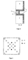
- FIG. 1 shows a side view of a flip-chip assembly with a microwave antenna according to the invention.
- the antenna is realized by the flip-chip mounting of two surface-metallized substrates a and b (metallization 1). These may also be semiconductor substrates with integrated circuits.
- the two substrates a and b are connected to the surfaces of each other by bumps 2.
- the result is a parallel-plate line structure with a lateral slot opening of the slot length d between the substrates a and b.
- This slot opening has a height h, which corresponds to the height h of the bumps 2.
- the height h is 50... 100 ⁇ m and is thus significantly smaller than the free-space wavelength ⁇ 0 for a frequency range from 10 to 150 GHz.
- the side walls 3 and 4 of the substrates a and b should be highly conductive to achieve the lateral directivity. They are therefore provided with a metallization 5, which is indicated here as continuous, but which may also be realized by Via fences on the edge of the substrates a and b appropriate.
- FIG. 2 shows a section in the plane AA 'in Figure 1, that is in the antenna plane
- Figure 3 is a section through the plane of symmetry BB' in Figure 2.
- the microwave antenna consists of a triangular cavity formed by the correspondingly arranged bumps 2 between the both substrates a and b. At the front, long side of the cavity for radiation is open (slot length d), on the other two sides it is shielded by a number of bumps 2. The distance between the bumps 2 is smaller than half the free space wavelength ⁇ 0/2. The slot length d must be approximately half the free space wavelength ⁇ 0/2, respectively.
- the antenna arrangement is similar to a horn, but acts due to the small height h and the conductive side walls 3 and 4 rather than slot antenna.
- the excitation of the antenna takes place locally between the two substrates a and b with an I / O bump 6. If necessary, this I / O bump 6 directly with a on connected to the substrate a and / or b integrated coplanar front-end circuit, which minimizes the feed losses. Since a coplanar circuit has interconnected ground planes and generally occupies only a small area of the triangular antenna space, this only leads to small changes in the antenna behavior.
- the microwave antenna shown works as a cavity resonator, which is attenuated by the radiation. This property can be used for narrowband transformation by optimizing the position of the I / O bump 6. This simultaneously provides a filtering effect: all frequencies outside the resonant frequency are poorly matched and are therefore attenuated.
- the resonance frequency is given essentially by the dimensions of the triangle formed by the bump 2.
- FIGS. 1 to 3 can be completed to form a four-sector antenna which, as shown in FIG. 4, then covers a 360 ° region.
- the substrates a and b were implemented as a gallium arsenide (GaAs) substrate (substrates a and b each 625 ⁇ m thick) with gold metallization.
- the slot length d was 12.5 mm.
- the conductive sidewalls 3, 4 were realized by means of via chains (diameter 400 ⁇ m, 1 mm pitch (center distance)).
- the bumps 2 were designed as gold-tin (AuSn) bumps with a diameter of about 80 microns, the chips were flip-chip soldered with a resulting height h of about 80 microns.
- the front-end circuits were arranged coplanar within a triangular antenna space (eg on the substrate a).
- the antenna was excited via an I / O bump 6, which connects the front end to the metallization 1 on the substrate b.
- the intermediate frequency or baseband output of the front-end circuits was carried by vias to the back of the substrate a.
Landscapes
- Engineering & Computer Science (AREA)
- Manufacturing & Machinery (AREA)
- Microelectronics & Electronic Packaging (AREA)
- Variable-Direction Aerials And Aerial Arrays (AREA)
- Waveguide Aerials (AREA)
- Details Of Aerials (AREA)
Description
- Die Erfindung betrifft eine Mikrowellenantenne für in Flip-Chip-Technologie hergestellte Halbleiterbaugruppen mit zwei an ihrer Oberfläche metallisierten Halbleitersubstraten.
- In Flip-Chip-Technologie realisierte Schaltungen sind weithin bekannt. Bei der Flip-Chip-Technologie werden in zwei Ebenen übereinander liegende Halbleitersubstrate miteinander verbunden. Beispielsweise kann ein Halbleiterchip mit einem Träger oder einem Grundsubstrat verbunden werden. Zur Verbindung der beiden Schaltungseinheiten werden anstelle von Drahtbonds sogenannte Bumps (Löt- oder hart plattierte Höcker) verwendet. Beispielsweise wird bei sogenannten Ball Bumps ein Draht an eines der Substrate angebondet und anschließend abgeschmolzen oder abgerissen. Dadurch entsteht eine elektrisch leitende Erhöhung (Höcker), die sich beim Aufeinandersetzen der beiden Substrate mit einer Kontaktstelle der gegenüberliegenden Seite, zum Beispiel durch Thermokompression, verbinden lässt.
- Auf den Substraten sind üblicherweise monolithisch integrierte Schaltungen aufgebaut, wobei die Bumps zur elektrischen Verbindung der Schaltungselemente dienen. Einzelne Bumps können jedoch auch allein aus Gründen der Abstandshalterung der beiden Substrate vorgesehen sein. Auch zur thermischen Ableitung werden die Bumps gern benutzt. Eine Flip-Chip-Baugruppe kann mit einer eigenen Sende- und/oder Empfangsantenne und gegebenenfalls mit einer eigenen Stromversorgung ausgerüstet werden, so dass autarke Sende/Empfangsbaugruppen entstehen. Bekannt sind sogenannte Patch-Antennen, das heißt metallisierte, von der übrigen Schaltung isolierte flächige Bereiche auf einer äußeren Oberfläche einer solchen Baugruppe mit einer Zuleitung zur Schaltung. Die Zuleitung kann gegebenenfalls durch eine vertikale Durchkontaktierung ("via") durch eines der Substrate realisiert werden.
- Aus
DE 691 18 060 T2 ist zum Beispiel ein Mikrowellen-Radar-Sender/Empfänger in Flip-Chip-Technologie auf der Grundlage eines monolithisch integrierten Mikrowellen-Schaltkreises (MMIC) bekannt, der zum Senden und Empfangen eines Nahbereichs-Radarsignals mit einer solchen Patch-Antenne ausgerüstet ist. Allgemeinere Erläuterungen zu Patch-Antennen finden sich in R. E. Munson, Conformed Microstrip Antennas and Microstrip Phases arrays, IEEE Transactions on Antennas and Propagation, Vol. 22, 1975 pp. 74-78 oder in J.-F. Zürcher, F. E. Gardiol, Broadband Patch Antennas, Boston, Artech House Inc., 1995. - Aus
US2002/0145566A1 ist eine Antenne vom Type Halbwellendipol bekannt, welche auf einem Halbleiter-Chip integriert ist und die den Oberbegriff des Anspruchs 1 bildet. - Die bekannten Antennen haben die Eigenschaft, dass sie eine vertikale Abstrahlung in einem relativ großen Winkel bewirken. Für bestimmte Anwendungen ist jedoch auch eine laterale Abstrahlung bzw. Empfang oder eine Rundum-Abstrahlung wünschenswert.
- Der Erfindung liegt die Aufgabe zugrunde, eine Mikrowellenantenne der eingangs genannten Art anzugeben, die auch eine laterale oder eine Rundum-Abstrahlung bzw. -empfang erlaubt.
- Erfindungsgemäß wird die Aufgabe gelöst durch die Merkmale des Anspruchs 1. Zweckmäßige Ausgestaltungen sind Gegenstand der Unteransprüche.
- Danach sind zwischen den an ihrer Oberfläche metallisierten Halbleitersubstraten ein geschlossener Zug von Bumps so angeordnet, dass der Abstand der Bumps zueinander kleiner ist als die halbe Wellenlänge des abzustrahlenden oder zu empfangenden Mikrowellen-Signals und an mindestens einem Seitenwandpaar der Halbleitersubstrate ein offener Abstrahlschlitz entsteht und dass zwischen den Bumps und dem Abstrahlschlitz ein mit der Schaltung der Halbleiterbaugruppe verbundener Bump angeordnet ist, über den die Anregung der Mikrowellenantenne erfolgt.
- Es entsteht mit den Bumps eine Parallelplatten-Leitungsstruktur mit einer lateralen Schlitzöffnung. Diese Schlitzöffnung hat eine Höhe, die der Höhe der Bumps entspricht.
- Der Abstrahlschlitz hat zweckmäßig eine Länge wie etwa die halbe Wellenlänge des abzustrahlenden oder zu empfangenden Mikrowellen-Signals. Die Höhe der Bumps sollte wesentlich kleiner sein als die Wellenlänge des abzustrahlenden oder zu empfangenden Mikrowellen-Signals.
- Die Anordnung der Bumps zusammen mit dem Abstrahlschlitz erfolgt bevorzugt in der Weise, dass sich im wesentlichen eine Dreieckform des Antennenraumes ergibt.
- Zu Erhöhung der lateralen Richtwirkung der Mikrowellenantenne sind die Seitenwände der Halbleitersubstrate im Bereich des Abstrahlschlitzes bevorzugt mindestens teilweise metallisiert.
- Die Mikrowellenantenne ermöglicht die Realisierung von lateral gerichtet strahlenden Antennen mit Hilfe der gängigen planaren Aufbautechniken. Mit den bei planaren Aufbauten üblichen Patch-Antennen war dies bisher nur in vertikaler Richtung möglich. Die Ausdehnung der Mikrowellenantenne beträgt dabei nur eine halbe Wellenlänge. Sie ist daher besonders für den Frequenzbereich zwischen 10 und 150 GHz geeignet und ermöglicht den Aufbau miniaturisierter integrierter Richtstrahler.
- Ein weiterer Vorteil der erfindungsgemäßen Mikrowellenantenne ist, dass auf der äußeren Oberfläche der Baugruppe nur wenig Fläche für eine Antenne belegt werden muss.
- Bei einer Anordnung von mehreren Mikrowellenantennen auf den Halbleitersubstraten kann ein Abstrahlwinkel von bis zu 360° erreicht werden. Die Mikrowellenantenne hat gegenüber den bisherigen Patch-Antennen außerdem den besonderen Vorteil, dass sie gleichzeitig als Filter genutzt werden kann, da der Bump, über den die Anregung der Mikrowellenantenne erfolgt, so positioniert werden kann, dass die Mikrowellenantenne nur für die Resonanzfrequenz eine Impedanzanpassung aufweist.
- In Kombination mit einer bzw. mehreren Patch-Antennen lässt sich mit der erfindungsgemäßen Mikrowellenantenne vorteilhaft eine Rundum-Abstrahlung in alle Raumrichtungen erreichen.
- Der Aufbau einer Baugruppe mit einer erfindungsgemäßen Mikrowellenantenne erfolgt nach der üblichen Flip-Chip-Technologie. Die Substrate werden mit Hilfe eines koplanaren MMIC-Prozesses (MMIC = Microwave Monolithic Integrated Circuits) hergestellt, entweder nur als Metallisierungen oder gegebenenfalls als Schaltungen. Im Rahmen der Rückseitenprozessierung werden zweckmäßig die Metallisierung der Seitenwände als Via-Zäune an den Rändern sowie die benötigten elektrischen Verbindungen von Vorder- und Rückseite als Vias realisiert. Anschließend erfolgt das Aufbringen der Bumps auf einem der Substrate und die Vereinzelung der Wafer zu Chips sowie schließlich das Flip-Chip-Bonden der beiden Chips (Substrate).
- Mit einem Aufbau gemäß der Erfindung lassen sich Halbleiterbaugruppen herstellen zum Beispiel für Nahfeld-Radarsysteme und andere Sensoren, Mikromodul-Etiketten sowie alle Arten von Chipkarten und ähnlichen Systemen, auch Einwegartikel, die über eine geringe Distanz im Gigahertzbereich kommunizieren. Eine Kombination mit den bisher üblichen Patch-Antennen ist ebenfalls möglich, so dass sich insgesamt eine kugelförmige Abstrahlung erreichen lässt.
- Die Erfindung soll nachstehend anhand von Ausführungsbeispielen näher erläutert werden. In den zugehörigen Zeichnungen zeigen
- Figur 1
- eine Seitenansicht einer Flip-Chip-Baugruppe mit einer erfindungsgemäßen Mikrowellenantenne,
- Figur 2
- eine Schnittansicht der Ebene A-A' in Figur 1 mit den erfindungsgemäßen Bump-Reihen und einer typischen Anregungsstelle E/A,
- Figur 3
- eine Schnittansicht der Ebene B-B' in Figur 2 und
- Figur 4
- eine Darstellung gemäß Figur 2 für den Fall einer Vier-Sektoren-Antenne.
- Figur 1 zeigt eine Seitenansicht einer Flip-Chip-Baugruppe mit einer erfindungsgemäßen Mikrowellenantenne. Die Antenne wird durch die Flip-Chip-Montage zweier an der Oberfläche metallisierter Substrate a und b realisiert (Metallisierung 1). Dabei kann es sich auch um Halbleitersubstrate mit integrierten Schaltungen handeln. Wie bei der Flip-Chip-Technik üblich, werden die beiden Substrate a und b mit den Oberflächen zueinander durch Bumps 2 verbunden. Es entsteht so eine Parallelplatten-Leitungsstruktur mit einer lateralen Schlitzöffnung der Schlitzlänge d zwischen den Substraten a und b. Diese Schlitzöffnung hat eine Höhe h, die der Höhe h der Bumps 2 entspricht. Typischerweise beträgt die Höhe h 50...100 µm und ist damit deutlich kleiner als die Freiraumwellenlänge λ0 für einen Frequenzbereich von 10 bis 150 GHz. Die Seitenwände 3 und 4 der Substrate a und b sollten zur Erzielung der lateralen Richtwirkung gut leitend sein. Sie sind deshalb mit einer Metallisierung 5 versehen, die hier als durchgehend angedeutet ist, die aber zweckmäßig auch durch Via-Zäune am Rand der Substrate a und b realisiert sein kann. Die gesamte Höhe des Schichtstapels da+db+h (da, db = Dicke der Substrate a, b) sollte nicht kleiner als ein Zehntel der Freiraumwellenlänge λ0 sein.
- Figur 2 zeigt einen Schnitt in der Ebene A-A' in Figur 1, das heißt in der Antennenebene, Figur 3 einen Schnitt durch die Symmetrieebene B-B' in Figur 2. Die Mikrowellenantenne besteht aus einem dreieckförmigen Hohlraum, gebildet durch die entsprechend angeordneten Bumps 2 zwischen den beiden Substraten a und b. An der vorderen, langen Seite ist der Hohlraum zur Abstrahlung offen (Schlitzlänge d), an den anderen beiden Seiten ist er durch jeweils eine Reihe von Bumps 2 geschirmt. Der Abstand der Bumps 2 ist kleiner als die halbe Freiraumwellenlänge λ0/2. Die Schlitzlänge d muss etwa die halbe Freiraumwellenlänge λ0/2 betragen. Die Antennenanordnung ähnelt einem Hornstrahler, wirkt aber wegen der geringen Höhe h und den leitenden Seitenwände 3 und 4 eher als Schlitzantenne.
- Die Anregung der Antenne, das heißt die Signaleinspeisung im Sende- bzw. das Ausgangstor im Empfangsfall, erfolgt lokal zwischen den beiden Substraten a und b mit einem E/A-Bump 6. Gegebenfalls kann dieser E/A-Bump 6 direkt mit einer auf dem Substrat a und/oder b integrierten koplanaren Frontend-Schaltung verbunden werden, was die Zuführungsverluste minimiert. Da eine koplanare Schaltung miteinander verbundene Masseflächen aufweist und im allgemeinen nur einen kleinen Bereich des dreieckigen Antennenraumes einnimmt, führt dies nur zu kleinen Veränderungen im Antennenverhalten.
- Die gezeigte Mikrowellenantenne arbeitet als Hohlraumresonator, der durch die Abstrahlung bedämpft wird. Diese Eigenschaft kann zur schmalbandigen Transformation genutzt werden, indem die Position des E/A-Bumps 6 optimiert wird. Dadurch erhält man gleichzeitig eine Filterwirkung: Alle Frequenzen außerhalb der Resonanzfrequenz sind schlecht angepasst und werden deshalb gedämpft. Die Resonanzfrequenz ist im wesentlichen durch die Abmessungen des durch die Bumps 2 gebildeten Dreiecks gegeben.
- Die Struktur gemäß den Figuren 1 bis 3 kann zu einer Vier-Sektorenantenne vervollständigt werden, die, wie in Figur 4 gezeigt ist, dann einen 360°-Bereich abdeckt.
- In einer konkreten Ausführungsform für eine 24 GHz-Antenne wurden die Substrate a und b als Galliumarsenid(GaAs)-Substrat (Substrate a und b jeweils 625 µm dick) mit Goldmetallisierung ausgeführt. Die Schlitzlänge d betrug 12,5 mm. Die leitenden Seitenwände 3, 4 wurden mit Hilfe von Via-Ketten realisiert (Durchmesser 400 µm, 1 mm Pitch (Abstand der Mittelpunkte)). Die Bumps 2 wurden als Gold-Zinn(AuSn)-Bumps ausgeführt mit einem Durchmesser von ca. 80 µm, die Chips wurden flip-chip-gelötet mit einer resultierenden Höhe h von ca. 80 µm. Die Frontend-Schaltungen wurden koplanar innerhalb eines dreieckförmigen Antennenraums angeordnet (z.B. auf dem Substrat a). Die Anregung der Antenne erfolgte über einen E/A-Bump 6, der das Frontend mit der Metallisierung 1 auf dem Substrat b verbindet. Der Zwischenfrequenz- oder Basisbandausgang der Frontend-Schaltungen wurde mittels Vias zur Rückseite des Substrats a ausgeführt.
-
- 1
- Metallisierung
- 2
- Bump
- 3
- Seitenwand
- 4
- Seitenwand
- 5
- Metallisierung
- 6
- E/A-Bump
- a, b
- Substrat
- d
- Schlitzlänge
- h
- Höhe
- da
- Dicke (des Substrats a)
- db
- Dicke (des Substrats b)
- λ0
- Freiraumwellenlänge
Claims (10)
- Mikrowellenantenne für in Flip-Chip-Technologie hergestellte Halbleiterbaugruppen, mit zwei an ihrer Oberfläche metallisierten Halbleitersubstraten (a, b),
dadurch gekennzeichnet, dass die beiden Substrate durch einen geschlossenen Zug von Bumps zwischen den metallisierten Oberflächen verbunden sind, wobei der Abstand der Bumps (2) zueinander kleiner ist als die halbe Wellenlänge (λ0/2) des abzustrahlenden oder zu empfangenden Mikrowellen-Signals und an mindestens einem Seitenwandpaar (3, 4) der Halbleitersubstrate (a, b) ein offener Abstrahlschlitz entsteht und dass zwischen den Bumps (2) und dem Abstrahlschlitz ein mit der Schaltung der Halbleiterbaugruppe verbundener Bump (6) angeordnet ist, über den die Anregung der Mikrowellenantenne erfolgt. - Mikrowellenantenne nach Anspruch 1, dadurch gekennzeichnet, dass die Anordnung der Bumps (2) zusammen mit dem Abstrahlschlitz im wesentlichen eine Dreieckform ergibt.
- Mikrowellenantenne nach Anspruch 1 oder 2, dadurch gekennzeichnet, dass die Schlitzlänge (d) des Abstrahlschlitzes etwa die halbe Wellenlänge (λ0/2) des abzustrahlenden oder zu empfangenden Mikrowellen-Signals beträgt.
- Mikrowellenantenne nach einem der vorhergehenden Ansprüche, dadurch gekennzeichnet, dass die Höhe (h) der Bumps (2) wesentlich kleiner ist als die Wellenlänge (λ0) des abzustrahlenden oder zu empfangenden Mikrowellen-Signals.
- Mikrowellenantenne nach einem der vorhergehenden Ansprüche, dadurch gekennzeichnet, dass die Bauhöhe der Halbleiterbaugruppe größer als ein Zehntel der Wellenlänge (λ0) des abzustrahlenden oder zu empfangenden Mikrowellen-Signals ist.
- Mikrowellenantenne nach einem der vorhergehenden Ansprüche, dadurch gekennzeichnet, dass die Seitenwände (3, 4) der Halbleitersubstrate im Bereich des Abstrahlschlitzes mindestens teilweise mit einer Metallisierung (5) versehen sind.
- Mikrowellenantenne nach einem der vorhergehenden Ansprüche, dadurch gekennzeichnet, dass der Bump (6), über den die Anregung der Mikrowellenantenne erfolgt, so positioniert ist, dass die Mikrowellenantenne bei der Resonanzfrequenz impedanzangepasst ist.
- Mikrowellenantenne nach einem der vorhergehenden Ansprüche, dadurch gekennzeichnet, dass auf mindestens einem der Halbleitersubstrate (a, b) im Bereich des durch die Bumps (2) und den Abstrahlschlitz aufgemachten Antennenraumes eine monolithisch integrierte Schaltung aufgebaut ist.
- Mikrowellenantenne nach einem der vorhergehenden Ansprüche, dadurch gekennzeichnet, dass zwischen den Halbleitersubstraten (a, b) Bumps (2) in einer kreuzförmigen Anordnung eingebracht sind, so dass eine Vier-Sektoren-Antenne entsteht.
- Mikrowellenantenne nach einem der vorhergehenden Ansprüche, dadurch gekennzeichnet, dass die Metallisierung (5) der Seitenwände der Halbleitersubstrate durch Via-Ketten realisiert ist.
Applications Claiming Priority (2)
| Application Number | Priority Date | Filing Date | Title |
|---|---|---|---|
| DE102004014018A DE102004014018B3 (de) | 2004-03-19 | 2004-03-19 | Mikrowellenantenne für in Flip-Chip-Technologie hergestellte Halbleiterbaugruppen |
| PCT/EP2005/003303 WO2005091438A1 (de) | 2004-03-19 | 2005-03-16 | Mikrowellenantenne für in flip-chip-technologie hergestellte halbleiterbaugruppen |
Publications (2)
| Publication Number | Publication Date |
|---|---|
| EP1726063A1 EP1726063A1 (de) | 2006-11-29 |
| EP1726063B1 true EP1726063B1 (de) | 2007-07-04 |
Family
ID=34745452
Family Applications (1)
| Application Number | Title | Priority Date | Filing Date |
|---|---|---|---|
| EP05728358A Expired - Lifetime EP1726063B1 (de) | 2004-03-19 | 2005-03-16 | Mikrowellenantenne für in flip-chip-technologie hergestellte halbleiterbaugruppen |
Country Status (6)
| Country | Link |
|---|---|
| US (1) | US7612728B2 (de) |
| EP (1) | EP1726063B1 (de) |
| JP (1) | JP2007529930A (de) |
| AT (1) | ATE366465T1 (de) |
| DE (2) | DE102004014018B3 (de) |
| WO (1) | WO2005091438A1 (de) |
Families Citing this family (11)
| Publication number | Priority date | Publication date | Assignee | Title |
|---|---|---|---|---|
| US9103902B2 (en) * | 2007-05-09 | 2015-08-11 | Infineon Technologies Ag | Packaged antenna and method for producing same |
| JP2009200101A (ja) | 2008-02-19 | 2009-09-03 | Liquid Design Systems:Kk | 半導体チップ及び半導体装置 |
| US8274136B2 (en) * | 2009-04-09 | 2012-09-25 | Worcester Polytechnic Institute | Semiconductor patch antenna |
| JP5429459B2 (ja) * | 2009-06-01 | 2014-02-26 | 独立行政法人情報通信研究機構 | ミリ波アンテナ |
| US8489162B1 (en) * | 2010-08-17 | 2013-07-16 | Amazon Technologies, Inc. | Slot antenna within existing device component |
| EP2667449A1 (de) * | 2012-05-23 | 2013-11-27 | Nxp B.V. | Integriertes Schaltungspaket mit integrierter Antenne |
| US9871299B2 (en) * | 2014-12-04 | 2018-01-16 | Qualcomm Incorporated | Cavity backed aperture antenna |
| US9443810B1 (en) | 2015-09-14 | 2016-09-13 | Qualcomm Incorporated | Flip-chip employing integrated cavity filter, and related components, systems, and methods |
| US11276915B2 (en) | 2017-03-27 | 2022-03-15 | Intel Corporation | Antennas integrated into a printed circuit board |
| JP7077402B2 (ja) * | 2017-10-05 | 2022-05-30 | グーグル エルエルシー | フリップチップ形状の低フットプリント共振器 |
| CN113659322B (zh) * | 2021-07-26 | 2024-04-19 | 西安理工大学 | 一种基于四分之一模的波束可重构基片集成波导天线 |
Family Cites Families (5)
| Publication number | Priority date | Publication date | Assignee | Title |
|---|---|---|---|---|
| US5115245A (en) * | 1990-09-04 | 1992-05-19 | Hughes Aircraft Company | Single substrate microwave radar transceiver including flip-chip integrated circuits |
| JP3141692B2 (ja) * | 1994-08-11 | 2001-03-05 | 松下電器産業株式会社 | ミリ波用検波器 |
| JP3471160B2 (ja) * | 1996-03-18 | 2003-11-25 | 株式会社東芝 | モノリシックアンテナ |
| US6563464B2 (en) | 2001-03-19 | 2003-05-13 | International Business Machines Corporation | Integrated on-chip half-wave dipole antenna structure |
| US6930647B2 (en) | 2001-05-17 | 2005-08-16 | Hitachi Kokusai Electric Inc. | Semicircular radial antenna |
-
2004
- 2004-03-19 DE DE102004014018A patent/DE102004014018B3/de not_active Expired - Fee Related
-
2005
- 2005-03-16 DE DE502005000985T patent/DE502005000985D1/de not_active Expired - Fee Related
- 2005-03-16 WO PCT/EP2005/003303 patent/WO2005091438A1/de not_active Ceased
- 2005-03-16 JP JP2007503307A patent/JP2007529930A/ja active Pending
- 2005-03-16 US US10/593,337 patent/US7612728B2/en not_active Expired - Fee Related
- 2005-03-16 EP EP05728358A patent/EP1726063B1/de not_active Expired - Lifetime
- 2005-03-16 AT AT05728358T patent/ATE366465T1/de not_active IP Right Cessation
Non-Patent Citations (1)
| Title |
|---|
| None * |
Also Published As
| Publication number | Publication date |
|---|---|
| US7612728B2 (en) | 2009-11-03 |
| DE502005000985D1 (de) | 2007-08-16 |
| US20080238792A1 (en) | 2008-10-02 |
| JP2007529930A (ja) | 2007-10-25 |
| EP1726063A1 (de) | 2006-11-29 |
| ATE366465T1 (de) | 2007-07-15 |
| DE102004014018B3 (de) | 2005-08-11 |
| WO2005091438A1 (de) | 2005-09-29 |
Similar Documents
| Publication | Publication Date | Title |
|---|---|---|
| DE102010001407B4 (de) | Integrierte Antennen auf Wafer-Ebene | |
| DE102011085348B4 (de) | Integrierte Antennen in einem Waferebenengehäuse und Herstellungsverfahren dafür | |
| DE60221353T2 (de) | Radarsensor | |
| DE102006023123B4 (de) | Abstandserfassungsradar für Fahrzeuge mit einem Halbleitermodul mit Komponenten für Höchstfrequenztechnik in Kunststoffgehäuse und Verfahren zur Herstellung eines Halbleitermoduls mit Komponenten für ein Abstandserfassungsradar für Fahrzeuge in einem Kunststoffgehäuse | |
| DE602004008653T2 (de) | Flexible konforme antenne | |
| DE69628253T2 (de) | Ultrahochfrequenzfunkgerät | |
| EP1245059B1 (de) | Radarsensor für ein überwachen der umgebung eines kraftfahrzeuges | |
| EP2820674B1 (de) | Halbleitermodul mit integrierten antennenstrukturen | |
| DE112008000985T5 (de) | Hochfrequenz-Leiterplatte, Hochfrequenz-Schaltmodul und Radargerät | |
| DE102004014018B3 (de) | Mikrowellenantenne für in Flip-Chip-Technologie hergestellte Halbleiterbaugruppen | |
| DE102020112787A1 (de) | Hochfrequenz-Vorrichtung mit Hochfrequenz-Chip und Hohlleiterstruktur | |
| DE3855146T2 (de) | Monolithischer Mikrowellen-Sender/Empfänger | |
| EP2494655B1 (de) | Antennenanordnung zur übertragung von signalen | |
| EP1825561B1 (de) | Antennenanordnung für einen radar-transceiver | |
| DE102013111569B4 (de) | Halbleiterpackages mit integrierter Antenne und Verfahren zu deren Herstellung | |
| EP1420267B1 (de) | Radarsensor und Radarantenne für ein Überwachen der Umgebung eines Kraftfahrzeugs | |
| DE112009002384T5 (de) | Antenne und Drahtlose-IC-Bauelement | |
| EP3503290B1 (de) | Antennenvorrichtung mit bonddrähten | |
| EP3346545B1 (de) | Bändchenbondantennen | |
| DE102013207829A1 (de) | Chip-Antenne, Elektronisches Bauelement und Herstellungsverfahren dafür | |
| DE102004059395A1 (de) | Sende- und/oder Empfangseinrichtung | |
| EP1958002A1 (de) | Antennenanordnung für einen radar-sensor | |
| DE102012025433B4 (de) | Verfahren zur Gehäusung von Sub-Millimeterwellen-Halbleiterschaltungen sowie mit dem Verfahren herstellbares Halbleitermodul | |
| DE102004013643A1 (de) | Antennenanordnung und Verfahren zum Herstellen derselben | |
| EP4016729A1 (de) | Antennenvorrichtung, antennenarray, elektrische schaltung mit einer antennenvorrichtung und bändchenbondantenne |
Legal Events
| Date | Code | Title | Description |
|---|---|---|---|
| PUAI | Public reference made under article 153(3) epc to a published international application that has entered the european phase |
Free format text: ORIGINAL CODE: 0009012 |
|
| 17P | Request for examination filed |
Effective date: 20060720 |
|
| AK | Designated contracting states |
Kind code of ref document: A1 Designated state(s): AT BE BG CH CY CZ DE DK EE ES FI FR GB GR HU IE IS IT LI LT LU MC NL PL PT RO SE SI SK TR |
|
| DAX | Request for extension of the european patent (deleted) | ||
| GRAP | Despatch of communication of intention to grant a patent |
Free format text: ORIGINAL CODE: EPIDOSNIGR1 |
|
| GRAS | Grant fee paid |
Free format text: ORIGINAL CODE: EPIDOSNIGR3 |
|
| GRAA | (expected) grant |
Free format text: ORIGINAL CODE: 0009210 |
|
| AK | Designated contracting states |
Kind code of ref document: B1 Designated state(s): AT BE BG CH CY CZ DE DK EE ES FI FR GB GR HU IE IS IT LI LT LU MC NL PL PT RO SE SI SK TR |
|
| REG | Reference to a national code |
Ref country code: GB Ref legal event code: FG4D Free format text: NOT ENGLISH |
|
| REG | Reference to a national code |
Ref country code: CH Ref legal event code: EP |
|
| REG | Reference to a national code |
Ref country code: IE Ref legal event code: FG4D Free format text: LANGUAGE OF EP DOCUMENT: GERMAN |
|
| GBT | Gb: translation of ep patent filed (gb section 77(6)(a)/1977) |
Effective date: 20070725 |
|
| REF | Corresponds to: |
Ref document number: 502005000985 Country of ref document: DE Date of ref document: 20070816 Kind code of ref document: P |
|
| ET | Fr: translation filed | ||
| NLV1 | Nl: lapsed or annulled due to failure to fulfill the requirements of art. 29p and 29m of the patents act | ||
| PG25 | Lapsed in a contracting state [announced via postgrant information from national office to epo] |
Ref country code: PT Free format text: LAPSE BECAUSE OF FAILURE TO SUBMIT A TRANSLATION OF THE DESCRIPTION OR TO PAY THE FEE WITHIN THE PRESCRIBED TIME-LIMIT Effective date: 20071204 Ref country code: FI Free format text: LAPSE BECAUSE OF FAILURE TO SUBMIT A TRANSLATION OF THE DESCRIPTION OR TO PAY THE FEE WITHIN THE PRESCRIBED TIME-LIMIT Effective date: 20070704 Ref country code: CZ Free format text: LAPSE BECAUSE OF FAILURE TO SUBMIT A TRANSLATION OF THE DESCRIPTION OR TO PAY THE FEE WITHIN THE PRESCRIBED TIME-LIMIT Effective date: 20070704 Ref country code: SI Free format text: LAPSE BECAUSE OF FAILURE TO SUBMIT A TRANSLATION OF THE DESCRIPTION OR TO PAY THE FEE WITHIN THE PRESCRIBED TIME-LIMIT Effective date: 20070704 Ref country code: LT Free format text: LAPSE BECAUSE OF FAILURE TO SUBMIT A TRANSLATION OF THE DESCRIPTION OR TO PAY THE FEE WITHIN THE PRESCRIBED TIME-LIMIT Effective date: 20070704 Ref country code: ES Free format text: LAPSE BECAUSE OF FAILURE TO SUBMIT A TRANSLATION OF THE DESCRIPTION OR TO PAY THE FEE WITHIN THE PRESCRIBED TIME-LIMIT Effective date: 20071015 Ref country code: BG Free format text: LAPSE BECAUSE OF FAILURE TO SUBMIT A TRANSLATION OF THE DESCRIPTION OR TO PAY THE FEE WITHIN THE PRESCRIBED TIME-LIMIT Effective date: 20071004 Ref country code: NL Free format text: LAPSE BECAUSE OF FAILURE TO SUBMIT A TRANSLATION OF THE DESCRIPTION OR TO PAY THE FEE WITHIN THE PRESCRIBED TIME-LIMIT Effective date: 20070704 Ref country code: IS Free format text: LAPSE BECAUSE OF FAILURE TO SUBMIT A TRANSLATION OF THE DESCRIPTION OR TO PAY THE FEE WITHIN THE PRESCRIBED TIME-LIMIT Effective date: 20071104 |
|
| PG25 | Lapsed in a contracting state [announced via postgrant information from national office to epo] |
Ref country code: PL Free format text: LAPSE BECAUSE OF FAILURE TO SUBMIT A TRANSLATION OF THE DESCRIPTION OR TO PAY THE FEE WITHIN THE PRESCRIBED TIME-LIMIT Effective date: 20070704 |
|
| REG | Reference to a national code |
Ref country code: IE Ref legal event code: FD4D |
|
| PG25 | Lapsed in a contracting state [announced via postgrant information from national office to epo] |
Ref country code: DK Free format text: LAPSE BECAUSE OF FAILURE TO SUBMIT A TRANSLATION OF THE DESCRIPTION OR TO PAY THE FEE WITHIN THE PRESCRIBED TIME-LIMIT Effective date: 20070704 Ref country code: GR Free format text: LAPSE BECAUSE OF FAILURE TO SUBMIT A TRANSLATION OF THE DESCRIPTION OR TO PAY THE FEE WITHIN THE PRESCRIBED TIME-LIMIT Effective date: 20071005 |
|
| PLBE | No opposition filed within time limit |
Free format text: ORIGINAL CODE: 0009261 |
|
| STAA | Information on the status of an ep patent application or granted ep patent |
Free format text: STATUS: NO OPPOSITION FILED WITHIN TIME LIMIT |
|
| PG25 | Lapsed in a contracting state [announced via postgrant information from national office to epo] |
Ref country code: IE Free format text: LAPSE BECAUSE OF FAILURE TO SUBMIT A TRANSLATION OF THE DESCRIPTION OR TO PAY THE FEE WITHIN THE PRESCRIBED TIME-LIMIT Effective date: 20070704 Ref country code: SK Free format text: LAPSE BECAUSE OF FAILURE TO SUBMIT A TRANSLATION OF THE DESCRIPTION OR TO PAY THE FEE WITHIN THE PRESCRIBED TIME-LIMIT Effective date: 20070704 |
|
| 26N | No opposition filed |
Effective date: 20080407 |
|
| PG25 | Lapsed in a contracting state [announced via postgrant information from national office to epo] |
Ref country code: SE Free format text: LAPSE BECAUSE OF FAILURE TO SUBMIT A TRANSLATION OF THE DESCRIPTION OR TO PAY THE FEE WITHIN THE PRESCRIBED TIME-LIMIT Effective date: 20071004 Ref country code: RO Free format text: LAPSE BECAUSE OF FAILURE TO SUBMIT A TRANSLATION OF THE DESCRIPTION OR TO PAY THE FEE WITHIN THE PRESCRIBED TIME-LIMIT Effective date: 20070704 |
|
| BERE | Be: lapsed |
Owner name: FORSCHUNGSVERBUND BERLIN E.V. Effective date: 20080331 |
|
| PG25 | Lapsed in a contracting state [announced via postgrant information from national office to epo] |
Ref country code: MC Free format text: LAPSE BECAUSE OF NON-PAYMENT OF DUE FEES Effective date: 20080331 |
|
| PG25 | Lapsed in a contracting state [announced via postgrant information from national office to epo] |
Ref country code: DE Free format text: LAPSE BECAUSE OF NON-PAYMENT OF DUE FEES Effective date: 20081001 Ref country code: EE Free format text: LAPSE BECAUSE OF FAILURE TO SUBMIT A TRANSLATION OF THE DESCRIPTION OR TO PAY THE FEE WITHIN THE PRESCRIBED TIME-LIMIT Effective date: 20070704 |
|
| PG25 | Lapsed in a contracting state [announced via postgrant information from national office to epo] |
Ref country code: BE Free format text: LAPSE BECAUSE OF NON-PAYMENT OF DUE FEES Effective date: 20080331 |
|
| PG25 | Lapsed in a contracting state [announced via postgrant information from national office to epo] |
Ref country code: CY Free format text: LAPSE BECAUSE OF FAILURE TO SUBMIT A TRANSLATION OF THE DESCRIPTION OR TO PAY THE FEE WITHIN THE PRESCRIBED TIME-LIMIT Effective date: 20070704 |
|
| PG25 | Lapsed in a contracting state [announced via postgrant information from national office to epo] |
Ref country code: AT Free format text: LAPSE BECAUSE OF NON-PAYMENT OF DUE FEES Effective date: 20080316 |
|
| REG | Reference to a national code |
Ref country code: CH Ref legal event code: PL |
|
| PG25 | Lapsed in a contracting state [announced via postgrant information from national office to epo] |
Ref country code: LI Free format text: LAPSE BECAUSE OF NON-PAYMENT OF DUE FEES Effective date: 20090331 Ref country code: CH Free format text: LAPSE BECAUSE OF NON-PAYMENT OF DUE FEES Effective date: 20090331 |
|
| PG25 | Lapsed in a contracting state [announced via postgrant information from national office to epo] |
Ref country code: LU Free format text: LAPSE BECAUSE OF NON-PAYMENT OF DUE FEES Effective date: 20080316 Ref country code: HU Free format text: LAPSE BECAUSE OF FAILURE TO SUBMIT A TRANSLATION OF THE DESCRIPTION OR TO PAY THE FEE WITHIN THE PRESCRIBED TIME-LIMIT Effective date: 20080105 |
|
| PG25 | Lapsed in a contracting state [announced via postgrant information from national office to epo] |
Ref country code: TR Free format text: LAPSE BECAUSE OF FAILURE TO SUBMIT A TRANSLATION OF THE DESCRIPTION OR TO PAY THE FEE WITHIN THE PRESCRIBED TIME-LIMIT Effective date: 20070704 |
|
| PG25 | Lapsed in a contracting state [announced via postgrant information from national office to epo] |
Ref country code: IT Free format text: LAPSE BECAUSE OF NON-PAYMENT OF DUE FEES Effective date: 20080331 |
|
| REG | Reference to a national code |
Ref country code: FR Ref legal event code: PLFP Year of fee payment: 11 |
|
| REG | Reference to a national code |
Ref country code: FR Ref legal event code: PLFP Year of fee payment: 12 |
|
| REG | Reference to a national code |
Ref country code: FR Ref legal event code: PLFP Year of fee payment: 13 |
|
| REG | Reference to a national code |
Ref country code: FR Ref legal event code: PLFP Year of fee payment: 14 |
|
| PGFP | Annual fee paid to national office [announced via postgrant information from national office to epo] |
Ref country code: GB Payment date: 20200325 Year of fee payment: 16 |
|
| PGFP | Annual fee paid to national office [announced via postgrant information from national office to epo] |
Ref country code: FR Payment date: 20200324 Year of fee payment: 16 |
|
| GBPC | Gb: european patent ceased through non-payment of renewal fee |
Effective date: 20210316 |
|
| PG25 | Lapsed in a contracting state [announced via postgrant information from national office to epo] |
Ref country code: FR Free format text: LAPSE BECAUSE OF NON-PAYMENT OF DUE FEES Effective date: 20210331 Ref country code: GB Free format text: LAPSE BECAUSE OF NON-PAYMENT OF DUE FEES Effective date: 20210316 |