EP1719246B1 - Bipolar differential input stage with input bias current cancellation circuit - Google Patents
Bipolar differential input stage with input bias current cancellation circuit Download PDFInfo
- Publication number
- EP1719246B1 EP1719246B1 EP04813977A EP04813977A EP1719246B1 EP 1719246 B1 EP1719246 B1 EP 1719246B1 EP 04813977 A EP04813977 A EP 04813977A EP 04813977 A EP04813977 A EP 04813977A EP 1719246 B1 EP1719246 B1 EP 1719246B1
- Authority
- EP
- European Patent Office
- Prior art keywords
- transistor
- current
- collector
- emitter
- base
- Prior art date
- Legal status (The legal status is an assumption and is not a legal conclusion. Google has not performed a legal analysis and makes no representation as to the accuracy of the status listed.)
- Expired - Lifetime
Links
- 230000003503 early effect Effects 0.000 claims description 5
- 230000004044 response Effects 0.000 claims description 3
- 230000008859 change Effects 0.000 description 2
- 230000003247 decreasing effect Effects 0.000 description 2
- 238000010586 diagram Methods 0.000 description 2
- 230000009467 reduction Effects 0.000 description 2
- 230000015556 catabolic process Effects 0.000 description 1
- 230000007423 decrease Effects 0.000 description 1
- 230000006872 improvement Effects 0.000 description 1
- 238000000034 method Methods 0.000 description 1
- 230000008569 process Effects 0.000 description 1
- 230000009897 systematic effect Effects 0.000 description 1
Images


Classifications
-
- H—ELECTRICITY
- H03—ELECTRONIC CIRCUITRY
- H03F—AMPLIFIERS
- H03F3/00—Amplifiers with only discharge tubes or only semiconductor devices as amplifying elements
- H03F3/04—Amplifiers with only discharge tubes or only semiconductor devices as amplifying elements with semiconductor devices only
- H03F3/08—Amplifiers with only discharge tubes or only semiconductor devices as amplifying elements with semiconductor devices only controlled by light
-
- H—ELECTRICITY
- H03—ELECTRONIC CIRCUITRY
- H03F—AMPLIFIERS
- H03F1/00—Details of amplifiers with only discharge tubes, only semiconductor devices or only unspecified devices as amplifying elements
- H03F1/56—Modifications of input or output impedances, not otherwise provided for
-
- H—ELECTRICITY
- H03—ELECTRONIC CIRCUITRY
- H03F—AMPLIFIERS
- H03F3/00—Amplifiers with only discharge tubes or only semiconductor devices as amplifying elements
- H03F3/45—Differential amplifiers
- H03F3/45071—Differential amplifiers with semiconductor devices only
- H03F3/45076—Differential amplifiers with semiconductor devices only characterised by the way of implementation of the active amplifying circuit in the differential amplifier
- H03F3/4508—Differential amplifiers with semiconductor devices only characterised by the way of implementation of the active amplifying circuit in the differential amplifier using bipolar transistors as the active amplifying circuit
- H03F3/45085—Long tailed pairs
- H03F3/45089—Non-folded cascode stages
-
- H—ELECTRICITY
- H03—ELECTRONIC CIRCUITRY
- H03F—AMPLIFIERS
- H03F3/00—Amplifiers with only discharge tubes or only semiconductor devices as amplifying elements
- H03F3/45—Differential amplifiers
- H03F3/45071—Differential amplifiers with semiconductor devices only
- H03F3/45479—Differential amplifiers with semiconductor devices only characterised by the way of common mode signal rejection
- H03F3/45484—Differential amplifiers with semiconductor devices only characterised by the way of common mode signal rejection in differential amplifiers with bipolar transistors as the active amplifying circuit
- H03F3/45488—Differential amplifiers with semiconductor devices only characterised by the way of common mode signal rejection in differential amplifiers with bipolar transistors as the active amplifying circuit by using feedback means
- H03F3/45515—Measuring at the active amplifying circuit of the differential amplifier
- H03F3/4552—Controlling the input circuit of the differential amplifier
-
- H—ELECTRICITY
- H03—ELECTRONIC CIRCUITRY
- H03F—AMPLIFIERS
- H03F3/00—Amplifiers with only discharge tubes or only semiconductor devices as amplifying elements
- H03F3/45—Differential amplifiers
- H03F3/45071—Differential amplifiers with semiconductor devices only
- H03F3/45479—Differential amplifiers with semiconductor devices only characterised by the way of common mode signal rejection
- H03F3/45484—Differential amplifiers with semiconductor devices only characterised by the way of common mode signal rejection in differential amplifiers with bipolar transistors as the active amplifying circuit
- H03F3/45596—Differential amplifiers with semiconductor devices only characterised by the way of common mode signal rejection in differential amplifiers with bipolar transistors as the active amplifying circuit by offset reduction
- H03F3/45618—Differential amplifiers with semiconductor devices only characterised by the way of common mode signal rejection in differential amplifiers with bipolar transistors as the active amplifying circuit by offset reduction by using balancing means
-
- H—ELECTRICITY
- H03—ELECTRONIC CIRCUITRY
- H03F—AMPLIFIERS
- H03F2200/00—Indexing scheme relating to amplifiers
- H03F2200/261—Amplifier which being suitable for instrumentation applications
-
- H—ELECTRICITY
- H03—ELECTRONIC CIRCUITRY
- H03F—AMPLIFIERS
- H03F2200/00—Indexing scheme relating to amplifiers
- H03F2200/453—Controlling being realised by adding a replica circuit or by using one among multiple identical circuits as a replica circuit
-
- H—ELECTRICITY
- H03—ELECTRONIC CIRCUITRY
- H03F—AMPLIFIERS
- H03F2203/00—Indexing scheme relating to amplifiers with only discharge tubes or only semiconductor devices as amplifying elements covered by H03F3/00
- H03F2203/45—Indexing scheme relating to differential amplifiers
- H03F2203/45538—Indexing scheme relating to differential amplifiers the IC comprising balancing means, e.g. trimming means
-
- H—ELECTRICITY
- H03—ELECTRONIC CIRCUITRY
- H03F—AMPLIFIERS
- H03F2203/00—Indexing scheme relating to amplifiers with only discharge tubes or only semiconductor devices as amplifying elements covered by H03F3/00
- H03F2203/45—Indexing scheme relating to differential amplifiers
- H03F2203/45541—Indexing scheme relating to differential amplifiers the IC comprising dynamic biasing means, i.e. controlled by the input signal
-
- H—ELECTRICITY
- H03—ELECTRONIC CIRCUITRY
- H03F—AMPLIFIERS
- H03F2203/00—Indexing scheme relating to amplifiers with only discharge tubes or only semiconductor devices as amplifying elements covered by H03F3/00
- H03F2203/45—Indexing scheme relating to differential amplifiers
- H03F2203/45576—Indexing scheme relating to differential amplifiers the IC comprising input impedance adapting or controlling means
Definitions
- This invention relates to the field of operational amplifiers (op amps), comparators, instrumentation amplifiers, and the like, and particularly to circuits designed to reduce the input bias currents in such circuits.
- the input stage of a bipolar circuit such as an op amp, comparator, or an instrumentation amplifier has an input bias current I B - i.e., the amount of current which flows into or out of the circuit's input terminals - of zero. This is because the resolution of the input stage increases with a decreasing I B .
- I B input bias current
- the output current I D of a photodiode is to be amplified by an op amp configured as an inverting amplifier, with a feedback resistance R.
- the op amp's output voltage V out will be given by (I D -T B )/R; i.e., the amount of photodiode current converted into an output voltage by the op amp is reduced by the magnitude of the op amp's input bias current.
- the input bias current I B of a bipolar input stage is non-zero because the stage's inputs are the bases of two bipolar transistors, arranged as a differential pair.
- One approach to reducing I B is to use input transistors with very high betas, known as "superbeta" transistors. However, though the use of a superbeta input pair can significantly reduce I B , it cannot eliminate it - and as such, the input bias currents and input current resolution will still be less than ideal.
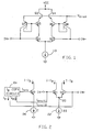
- bipolar input transistors Q1 and Q2 form a differential input pair.
- the common emitters of Q1 and Q2 are connected to a bias current source 10, and their collectors are coupled to respective biasing transistors Q3 and Q4.
- a "tracking" transistor Q5 is connected in series between Q1 and Q3, and another tracking transistor Q6 is connected in series between Q2 and Q4, such that the collector-emitter circuits of Q5 and Q6 conduct the collector currents of Q1 and Q2, respectively. This results in the base currents of Q5 and Q6 tracking those of Q1 and Q2, respectively.
- Lateral PNP transistors Q7 and Q8 are connected to mirror the base currents of Q5 and Q6 to the bases of Q1 and Q2, respectively.
- these mirrored currents effectively cancel the input bias currents of Q1 and Q2.
- the collector currents of Q7 and Q8 may not accurately track the base currents of Q5 and Q6, and, hence, may not accurately cancel the bias currents of their associated input transistors.
- U.S. Patent No. 4,575,685 to Dobkin et al . is designed to overcome the leakage current problem noted above, by employing circuitry including a tracking transistor which is virtually independent of the presence or absence of leakage current.
- the patent employs a scheme to make the collector-emitter voltages of the input and tracking transistors equal.
- the scheme used is subject to process variations that might result in unequal collector-emitter voltages, and a consequent lack of accuracy in the cancellation currents.
- U.S. Patent No. 6,636,111 to Gross et al discloses a prior art bipolar differential input stage which includes an input bias current cancellation circuit comprising: first and second bipolar input transistors having their bases connected to first and second input terminals, respectively, and their emitters connected together at a common emitter node, said first and second transistors arranged to be biased to conduct respective output currents in response to a differential input signal applied to said first and second input terminals; a bipolar tracking transistor; a first current source connected to said common emitter node; a second current source; and a base current copy circuit arranged to provide a base current to said tracking transistor, said base current copy circuit further arranged to provide first and second bias current cancellation currents to the bases of said first and second input transistors, respectively, thereby reducing the input stages' input bias currents.
- first and second bipolar input transistors having their bases connected to first and second input terminals, respectively, and their emitters connected together at a common emitter node, said first and second transistors arranged to be biased to
- a bipolar differential input stage with an input bias current cancellation circuit is presented which overcomes the problems noted above, reducing input bias currents down to the picoampere level.
- the present invention comprises a bipolar differential input stage as defined in claim 1.
- a bipolar differential input pair comprises first and second transistors Q1 and Q2, having their emitters connected to a common emitter node 20 and their bases connected to respective input terminals IN+ and IN-.
- a first current source 22 is connected to common emitter node 20 and provides bias current to Q1 and Q2 such that they conduct respective output currents in response to differential input signal applied to IN+ and IN-.
- Circuitry for reducing the input bias currents of Q1 and Q2 includes a tracking transistor Q3 and a base current copy circuit 24.
- a current source 26 provides bias current to Q3.
- the first and second current sources are arranged such that second current source 26 provides a bias current I, and first current source 22 provides a bias current 2*I. Then, when IN+ and IN- are equal , Q1 and Q2 each conduct currents I-IB, where IB is the base current of Q1 and Q2. Currents IB are the input bias currents which are intended to be reduced or cancelled.
- Circuitry (not shown) provides current to the collector of tracking transistor Q3 such that Q3 also conducts a current I-I B , where I B is the base current of Q3.
- the input stage is also arranged to ensure that the collector-emitter voltages of Q1, Q2 and Q3 are substantially equal. With Q1-Q3 having equal collector currents and equal collector-emitter voltages (when IN+ ⁇ IN-), Q3's base current will be substantially equal to that of Q1 and Q2.
- Q3's base current is defined by its collector current and its collector-emitter voltage.
- Base current copy circuit 24 is arranged to provide the base current I trk to tracking transistor Q3 required to make its collector current equal to those in Q1 and Q2.
- Copy circuit 24 replicates I trx and provides the copies as first and second bias current cancellation currents I cncl1 , I cncl2 to the bases of Q1 and Q2, respectively, such that I cncl1 ⁇ I cncl2 ⁇ I trk ⁇ I B .
- collector currents and collector-emitter voltages of Q1-Q3 substantially equal reduces cancellation current inaccuracies that might arise due to the Early effect, and ensures that the base current of Q3 will equal those of Q1 and Q2 with a high degree of precision. Under these conditions, when the base current of Q3 is copied to the bases of Q1 and Q2, the input pairs' input bias currents can be reduced down to the picoampere level.
- Q1-Q3 are preferably superbeta transistors, which inherently reduce the base current needed for a particular collector current, and thus serve to further reduce the input pairs' input bias currents. For best results, Q1-Q3 should have matching characteristics - particularly with respect to emitter size, temperature coefficient, and beta.
- Q1 and Q2 form a bipolar differential input pair, connected to input terminals IN+ and IN-, respectively. Their emitters are connected to a common emitter node 30. A current source 32 is connected to node 30 to provide bias current to Q1 and Q2.
- the collectors of Q1 and Q2 are connected to the emitters of respective cascode transistors Q4 and Q5, with the bases of Q4 and Q5 connected together at a node 34; the collectors of Q4 and Q5 are coupled to a supply voltage VCC (connection to VCC not shown).
- VCC supply voltage
- tracking transistor Q3 has its emitter connected to common emitter node 30 such that it is biased by current source 32.
- Q3's collector is connected to the collector-emitter circuit of a cascode transistor Q6 having its base connected to node 32, such that Q6 conducts Q3's collector current.
- Current source 32 is arranged to provide a bias current given by 3*I to common emitter node 30, and a current source 36 is arranged to provide a current.I to the collector of cascode transistor Q6.
- a current source 36 is arranged to provide a current.I to the collector of cascode transistor Q6.
- Base current copy circuit 24 is implemented with a lateral PNP transistor Q7, having a first collector connected to the base of tracking transistor Q3, a second collector connected to the base of Q1, and a third collector connected to the base of Q2.
- Q7 must be biased to operate in its linear region - i.e., with its emitter-base junction forward-biased and its base-collector junction reverse-biased - so that the current provided to Q3 via Q7's first collector is replicated on its second and third collectors.
- FIG. 3 One way of biasing Q7 as specified above is shown in FIG. 3 .
- the base of Q7 is connected to a node 38.
- a PNP transistor Q8 has its collector-emitter circuit connected between node 38 and a circuit common point 40, typically the negative supply (VEE).
- a current source 42 and a diode-connected NPN transistor Q9 are connected in series between supply voltage VCC and node 38.
- the emitter of Q7 is connected to the collector of Q6. This arrangement ensures that the voltages at Q7's base and emitter are such that its emitter-base junction is forward-biased, and that the voltages at Q7's base and collector are such that its collector-base junction is reverse-biased. This remains true even if the input common mode voltage changes, since node 38 varies with input common mode voltage, and the collector of Q6 is a floating, high impedance node.
- diode-connected Q9 also ensures that node 34 is one base-emitter voltage above the input common mode voltage, to keep the base-collector voltages of Q1-Q3 equal to zero. This protects superbeta devices, which tend to have low base-collector breakdown voltages.
- the arrangement of current sources 32 and 36 cause Q1, Q2, and Q3 to have substantially equal collector currents I. Because the bases of cascode transistors Q4, Q5 and Q6 are all connected together at node 34, the collectors of Q1-Q3 will be at equal voltages - one base-emitter junction voltage below node 34. The emitters of Q1-Q3 are connected together at common emitter node 30. As a result, the collector-emitter voltages of Q1, Q2 and Q3 will be substantially equal.
- collector currents and collector-emitter voltages of Q1-Q3 substantially equal reduces inaccuracies that might arise due to the Early effect, and ensures that the base current of Q3 will equal those of Q1 and Q2 with a high degree of precision.
- Lateral PNP transistor Q7 is connected to provide base current (I trk ) to tracking transistor Q3 via its first collector.
- Q7 replicates current I trk to the bases of Q1 and Q2 (as cancellation currents I cncl1 and I cncl2 ) via its second and third collectors, respectively. Since I trk is substantially equal to the base currents of Q1 and Q2, and I cnc1 ⁇ I cncl2 ⁇ I trk , I cncl1 and I cncl2 will substantially reduce the input bias currents of Q1 and Q2, respectively.
- current source 32 is implemented with a NPN transistor Q10 with an emitter resistor R1; R1 may be implemented with a single resistor or 3 resistors (R1a, R1b, R1c), preferably of equal resistance, connected in parallel.
- Current source 36 is preferably implemented with a transistor Q11 having its emitter coupled to circuit common point 40 via a resistor R2; the bases of Q11 and Q10 are connected together and to a common bias voltage V B .
- a diode-connected NPN transistor Q12 is connected between the collector of Q11 and a current mirror made from a diode-connected PNP transistor Q13 and a PNP transistor Q14.
- current source 32 provides a bias current given by 3*I and Q11 conducts a current I.
- Q11's current I is mirrored by the Q13/Q14 current mirror to the collector of Q6, thereby ensuring that, when IN+ ⁇ IN-, tracking transistor Q3 has a collector current I equal to the collector currents of Q1 and Q2.
- Current source 42 is here replaced with a resistor R3 connected between Q9 and a node 50, and Q13 and Q14 are connected to node 50 via respective resistors R4 and R5.
- Node 50 is connected to supply voltage VCC via a PNP transistor Q15.
- R3 is needed to ensure enough headroom for the Q13/Q14 current mirror.
- Q15 also serves to decouple the input bias current cancellation circuit from VCC. Because of Q15, the voltage at node 50 can vary with the input common mode voltage. As such, the biasing of the cancellation circuit's devices does not change with a change of the input common mode voltage. If node 50 was connected directly to VCC, the cancellation scheme would be input common mode voltage dependant.
- a voltage loop is formed between the collector of Q10 and the collector of Q11, via the base-emitter junctions of Q8 and Q9, R3, R4, and the base-emitter junctions of Q13 and Q12.
- This loop makes the collector voltages of Q10 and Q11 approximately equal, and enables them to vary equally with a varying input common mode voltage. For example, if the input common mode voltage decreases, the voltage loop ensures that the collector-emitter voltages across Q10 and Q11 are reduced by equal amounts, as are their collector currents. Therefore, the 3:1 ratio between the collector currents is kept constant for a changing input common mode voltage, which prevents cancellation current errors from being introduced due to the Early effect when the input common mode voltage changes.
- Mirror transistor Q13 preferably includes a resistor R6 connected between its collector and base. This serves to overdrive mirror transistor Q14 and thereby compensate for the emitter current of Q7 which is diverted from the collector of Q6 (and therefore Q3).
- the present input stage and input bias current cancellation circuit can be employed in numerous applications which use a bipolar differential input stage. Examples of such applications include op amps, comparators, and instrumentation amplifiers.
- a significant reduction in input bias current can be achieved; i.e., a typical base current of ⁇ 15 ⁇ A is reduced to -0.3 ⁇ A/ ⁇ , where ⁇ is the beta value of the input pair and tracking transistor.
- ⁇ is the beta value of the input pair and tracking transistor.
- Q1, Q2 and Q3 are each superbeta transistors with a ⁇ of 3000, the input stage's input bias current will be reduced to about 100pA. This greatly improves the input stage's input current resolution, which can be particularly advantageous when coupled to small input current such as that produced by a photodiode. This improvement is achieved without the need to perform a final resistor trim step.
- Additional input bias current reduction can be achieved with the addition of a trim step that trims the resistance values of resistors R4 and/or R5 in FIG. 4 , which adjusts the magnitude of the current through tracking transistor Q3. Note that Q3's current can be increased or decreased, depending on whether R4 or R5 is trimmed.
Landscapes
- Engineering & Computer Science (AREA)
- Power Engineering (AREA)
- Amplifiers (AREA)
- Control Of Electrical Variables (AREA)
- Manipulation Of Pulses (AREA)
Applications Claiming Priority (2)
| Application Number | Priority Date | Filing Date | Title |
|---|---|---|---|
| US10/789,738 US6965267B2 (en) | 2004-02-27 | 2004-02-27 | Bipolar differential input stage with input bias current cancellation circuit |
| PCT/US2004/041734 WO2005093947A1 (en) | 2004-02-27 | 2004-12-14 | Bipolar differential input stage with input bias current cancellation circuit |
Publications (2)
| Publication Number | Publication Date |
|---|---|
| EP1719246A1 EP1719246A1 (en) | 2006-11-08 |
| EP1719246B1 true EP1719246B1 (en) | 2010-06-30 |
Family
ID=34887358
Family Applications (1)
| Application Number | Title | Priority Date | Filing Date |
|---|---|---|---|
| EP04813977A Expired - Lifetime EP1719246B1 (en) | 2004-02-27 | 2004-12-14 | Bipolar differential input stage with input bias current cancellation circuit |
Country Status (5)
| Country | Link |
|---|---|
| US (1) | US6965267B2 (https=) |
| EP (1) | EP1719246B1 (https=) |
| JP (1) | JP4560541B2 (https=) |
| DE (1) | DE602004027956D1 (https=) |
| WO (1) | WO2005093947A1 (https=) |
Families Citing this family (16)
| Publication number | Priority date | Publication date | Assignee | Title |
|---|---|---|---|---|
| US7116174B2 (en) * | 2004-09-29 | 2006-10-03 | Agere Systems Inc. | Base current compensation circuit for a bipolar junction transistor |
| US7564309B2 (en) * | 2006-08-31 | 2009-07-21 | National Semiconductor Corportaion | Wide input common mode for input bias current cancellation |
| US7649417B1 (en) * | 2007-05-23 | 2010-01-19 | National Semiconductor Corporation | Apparatus and method for input stage and bias canceller for an audio operational amplifier |
| US8130037B2 (en) * | 2010-03-23 | 2012-03-06 | Analog Devices, Inc. | Apparatus and method for reducing current noise |
| US8258868B2 (en) * | 2010-11-10 | 2012-09-04 | Texas Instruments Incorporated | Differential input for ambipolar devices |
| US8416008B2 (en) * | 2011-01-20 | 2013-04-09 | Advanced Energy Industries, Inc. | Impedance-matching network using BJT switches in variable-reactance circuits |
| CN103365327A (zh) * | 2012-03-30 | 2013-10-23 | 苏州贝克微电子有限公司 | 一种将输入偏置电流减小到微微安级的电路 |
| US9671228B2 (en) | 2014-10-21 | 2017-06-06 | Honeywell International Inc. | Floating current mirror for RLG discharge control |
| US10992271B2 (en) | 2018-12-24 | 2021-04-27 | Texas Instruments Incorporated | Amplifier with input bias current cancellation |
| CN110048675B (zh) * | 2019-05-06 | 2023-03-21 | 西安微电子技术研究所 | 一种提高双极型轨对轨运放输入偏置电流性能的电路 |
| EP3806328B1 (en) * | 2019-10-08 | 2022-08-17 | Photolitics OOD | Comparator device for comparing an analog signal with a reference signal |
| JP7586686B2 (ja) * | 2020-10-30 | 2024-11-19 | 日清紡マイクロデバイス株式会社 | 入力バイアス電流低減回路 |
| JP7712074B2 (ja) * | 2020-11-20 | 2025-07-23 | 日清紡マイクロデバイス株式会社 | 増幅回路 |
| CN112928998B (zh) * | 2021-02-04 | 2023-11-17 | 苏州锐度微电子技术有限公司 | 一种双极型晶体管放大器 |
| CN114513177B (zh) * | 2021-12-31 | 2023-03-24 | 贵州振华风光半导体股份有限公司 | 一种基于双极型放大器的超低偏置电流设计方法及其电路 |
| US12323109B2 (en) | 2022-01-27 | 2025-06-03 | Analog Devices, Inc. | Low-headroom dynamic base current cancellation techniques |
Family Cites Families (18)
| Publication number | Priority date | Publication date | Assignee | Title |
|---|---|---|---|---|
| GB1234759A (en) * | 1967-12-13 | 1971-06-09 | Pressac Ltd | Contact bearing devices for securing to a board or the like having printed or like circuitry |
| US4068254A (en) * | 1976-12-13 | 1978-01-10 | Precision Monolithics, Inc. | Integrated FET circuit with input current cancellation |
| JPS581306A (ja) * | 1981-06-26 | 1983-01-06 | Nippon Kogaku Kk <Nikon> | 高入力インピ−ダンス差動増幅回路 |
| JPS5917712A (ja) * | 1982-07-21 | 1984-01-30 | Mitsubishi Electric Corp | ベ−ス電流補正回路 |
| JPS5983410A (ja) * | 1982-11-05 | 1984-05-14 | Toshiba Corp | 差動入力回路 |
| US4575658A (en) * | 1983-12-23 | 1986-03-11 | Honeywell Inc. | Power supply for a ring laser |
| JPS6112110A (ja) * | 1984-06-28 | 1986-01-20 | Toshiba Corp | 差動増幅器 |
| US4575685A (en) * | 1984-08-03 | 1986-03-11 | Linear Technology Corporation | Arrangement for cancelling the input bias current, at picoampere levels, in an integrated circuit |
| US4639684A (en) * | 1984-11-06 | 1987-01-27 | Harris Corporation | Differential input stage for the realization of low noise and high precision bipolar transistor amplifiers |
| US4755770A (en) * | 1986-08-13 | 1988-07-05 | Harris Corporation | Low noise current spectral density input bias current cancellation scheme |
| US4780688A (en) * | 1987-05-07 | 1988-10-25 | Harris Corporation | Large signal output current enhancement for a differential pair |
| US4843342A (en) * | 1987-12-09 | 1989-06-27 | Vtc Incorporated | Differential amplifier with input bias current cancellation |
| US4855684A (en) * | 1988-10-14 | 1989-08-08 | Analog Devices, Inc. | Bias current compensation for bipolar input stages |
| JPH02206907A (ja) * | 1989-02-07 | 1990-08-16 | Yokogawa Electric Corp | 差動増幅回路 |
| JP3125282B2 (ja) * | 1996-01-16 | 2001-01-15 | ローム株式会社 | オーディオ信号増幅回路およびこれを用いた携帯用音響機器 |
| US6469578B1 (en) * | 2001-05-23 | 2002-10-22 | Fairchild Semiconductor Corporation | Differential current mode gain stage and methods of using the same |
| US6549072B1 (en) * | 2002-01-16 | 2003-04-15 | Medtronic, Inc. | Operational amplifier having improved input offset performance |
| US6636111B1 (en) * | 2002-07-26 | 2003-10-21 | Linear Technology Corporation | Bootstrap circuit to cancel input bias currents of a differential amplifier over most of common-mode input voltage range |
-
2004
- 2004-02-27 US US10/789,738 patent/US6965267B2/en not_active Expired - Lifetime
- 2004-12-14 WO PCT/US2004/041734 patent/WO2005093947A1/en not_active Ceased
- 2004-12-14 EP EP04813977A patent/EP1719246B1/en not_active Expired - Lifetime
- 2004-12-14 JP JP2007500752A patent/JP4560541B2/ja not_active Expired - Fee Related
- 2004-12-14 DE DE602004027956T patent/DE602004027956D1/de not_active Expired - Lifetime
Also Published As
| Publication number | Publication date |
|---|---|
| WO2005093947A1 (en) | 2005-10-06 |
| US6965267B2 (en) | 2005-11-15 |
| EP1719246A1 (en) | 2006-11-08 |
| JP2007526693A (ja) | 2007-09-13 |
| JP4560541B2 (ja) | 2010-10-13 |
| DE602004027956D1 (de) | 2010-08-12 |
| US20050189992A1 (en) | 2005-09-01 |
Similar Documents
| Publication | Publication Date | Title |
|---|---|---|
| EP1719246B1 (en) | Bipolar differential input stage with input bias current cancellation circuit | |
| US4999585A (en) | Circuit technique for cancelling non-linear capacitor-induced harmonic distortion | |
| US6429700B1 (en) | Driver circuit with output common mode voltage control | |
| US4555673A (en) | Differential amplifier with rail-to-rail input capability and controlled transconductance | |
| JP2549540B2 (ja) | レベルシフト回路 | |
| US6426669B1 (en) | Low voltage bandgap reference circuit | |
| US7636016B2 (en) | Current mirror circuit | |
| US7395308B1 (en) | Grounded emitter logarithmic circuit | |
| US6483382B1 (en) | Current compensation circuit for improved open-loop gain in an amplifier | |
| US4654602A (en) | Current mirror circuit | |
| US6194886B1 (en) | Early voltage and beta compensation circuit for a current mirror | |
| US7683715B2 (en) | Feedback biasing technique for a stage of an amplifier that uses a feedback control loop having low gain | |
| US7068106B2 (en) | Bias current cancellation for differential amplifiers | |
| US4216436A (en) | High gain differential amplifier | |
| US5140181A (en) | Reference voltage source circuit for a Darlington circuit | |
| US12366877B2 (en) | Gain and temperature tolerant bandgap voltage reference | |
| US20020089371A1 (en) | Pair of bipolar transistor complementary current sources with base current compensation | |
| CN111969964B (zh) | 半导体运算放大装置和半导体感测装置 | |
| US6218894B1 (en) | Voltage and/or current reference circuit | |
| US5498952A (en) | Precise current generator | |
| JP4749368B2 (ja) | 差動増幅回路 | |
| US5942941A (en) | Base-current compensation circuit to reduce input offset voltage in a bipolar operational amplifier | |
| EP0384510B1 (en) | Differential amplifier | |
| US11258414B2 (en) | Compact offset drift trim implementation | |
| US6392489B1 (en) | Precise integrated current mirrors |
Legal Events
| Date | Code | Title | Description |
|---|---|---|---|
| PUAI | Public reference made under article 153(3) epc to a published international application that has entered the european phase |
Free format text: ORIGINAL CODE: 0009012 |
|
| 17P | Request for examination filed |
Effective date: 20060907 |
|
| AK | Designated contracting states |
Kind code of ref document: A1 Designated state(s): DE FR GB |
|
| DAX | Request for extension of the european patent (deleted) | ||
| RBV | Designated contracting states (corrected) |
Designated state(s): DE FR GB |
|
| 17Q | First examination report despatched |
Effective date: 20071228 |
|
| GRAP | Despatch of communication of intention to grant a patent |
Free format text: ORIGINAL CODE: EPIDOSNIGR1 |
|
| GRAS | Grant fee paid |
Free format text: ORIGINAL CODE: EPIDOSNIGR3 |
|
| GRAA | (expected) grant |
Free format text: ORIGINAL CODE: 0009210 |
|
| AK | Designated contracting states |
Kind code of ref document: B1 Designated state(s): DE FR GB |
|
| REG | Reference to a national code |
Ref country code: GB Ref legal event code: FG4D |
|
| REF | Corresponds to: |
Ref document number: 602004027956 Country of ref document: DE Date of ref document: 20100812 Kind code of ref document: P |
|
| PLBE | No opposition filed within time limit |
Free format text: ORIGINAL CODE: 0009261 |
|
| STAA | Information on the status of an ep patent application or granted ep patent |
Free format text: STATUS: NO OPPOSITION FILED WITHIN TIME LIMIT |
|
| 26N | No opposition filed |
Effective date: 20110331 |
|
| REG | Reference to a national code |
Ref country code: DE Ref legal event code: R097 Ref document number: 602004027956 Country of ref document: DE Effective date: 20110330 |
|
| REG | Reference to a national code |
Ref country code: FR Ref legal event code: ST Effective date: 20110831 |
|
| PG25 | Lapsed in a contracting state [announced via postgrant information from national office to epo] |
Ref country code: FR Free format text: LAPSE BECAUSE OF NON-PAYMENT OF DUE FEES Effective date: 20110103 |
|
| PGFP | Annual fee paid to national office [announced via postgrant information from national office to epo] |
Ref country code: GB Payment date: 20211118 Year of fee payment: 18 Ref country code: DE Payment date: 20211117 Year of fee payment: 18 |
|
| REG | Reference to a national code |
Ref country code: DE Ref legal event code: R119 Ref document number: 602004027956 Country of ref document: DE |
|
| GBPC | Gb: european patent ceased through non-payment of renewal fee |
Effective date: 20221214 |
|
| PG25 | Lapsed in a contracting state [announced via postgrant information from national office to epo] |
Ref country code: GB Free format text: LAPSE BECAUSE OF NON-PAYMENT OF DUE FEES Effective date: 20221214 Ref country code: DE Free format text: LAPSE BECAUSE OF NON-PAYMENT OF DUE FEES Effective date: 20230701 |