EP1719098B1 - Tiled display - Google Patents
Tiled display Download PDFInfo
- Publication number
- EP1719098B1 EP1719098B1 EP05714051A EP05714051A EP1719098B1 EP 1719098 B1 EP1719098 B1 EP 1719098B1 EP 05714051 A EP05714051 A EP 05714051A EP 05714051 A EP05714051 A EP 05714051A EP 1719098 B1 EP1719098 B1 EP 1719098B1
- Authority
- EP
- European Patent Office
- Prior art keywords
- display
- flat
- panel displays
- tiled
- lightpipes
- Prior art date
- Legal status (The legal status is an assumption and is not a legal conclusion. Google has not performed a legal analysis and makes no representation as to the accuracy of the status listed.)
- Expired - Lifetime
Links
- 230000002950 deficient Effects 0.000 claims description 14
- 238000004519 manufacturing process Methods 0.000 claims description 12
- 239000004973 liquid crystal related substance Substances 0.000 claims description 5
- 238000000034 method Methods 0.000 description 9
- 238000010586 diagram Methods 0.000 description 6
- 239000000758 substrate Substances 0.000 description 6
- 238000012937 correction Methods 0.000 description 5
- 230000000295 complement effect Effects 0.000 description 3
- 239000000835 fiber Substances 0.000 description 3
- 238000003384 imaging method Methods 0.000 description 3
- 230000008901 benefit Effects 0.000 description 2
- 238000012360 testing method Methods 0.000 description 2
- 239000000853 adhesive Substances 0.000 description 1
- 230000001070 adhesive effect Effects 0.000 description 1
- 238000013459 approach Methods 0.000 description 1
- 238000003491 array Methods 0.000 description 1
- 238000010276 construction Methods 0.000 description 1
- 230000000694 effects Effects 0.000 description 1
- 230000007246 mechanism Effects 0.000 description 1
- 230000003287 optical effect Effects 0.000 description 1
- 238000012545 processing Methods 0.000 description 1
- 230000035945 sensitivity Effects 0.000 description 1
- 230000001131 transforming effect Effects 0.000 description 1
Images


Classifications
-
- G—PHYSICS
- G02—OPTICS
- G02F—OPTICAL DEVICES OR ARRANGEMENTS FOR THE CONTROL OF LIGHT BY MODIFICATION OF THE OPTICAL PROPERTIES OF THE MEDIA OF THE ELEMENTS INVOLVED THEREIN; NON-LINEAR OPTICS; FREQUENCY-CHANGING OF LIGHT; OPTICAL LOGIC ELEMENTS; OPTICAL ANALOGUE/DIGITAL CONVERTERS
- G02F1/00—Devices or arrangements for the control of the intensity, colour, phase, polarisation or direction of light arriving from an independent light source, e.g. switching, gating or modulating; Non-linear optics
- G02F1/01—Devices or arrangements for the control of the intensity, colour, phase, polarisation or direction of light arriving from an independent light source, e.g. switching, gating or modulating; Non-linear optics for the control of the intensity, phase, polarisation or colour
- G02F1/13—Devices or arrangements for the control of the intensity, colour, phase, polarisation or direction of light arriving from an independent light source, e.g. switching, gating or modulating; Non-linear optics for the control of the intensity, phase, polarisation or colour based on liquid crystals, e.g. single liquid crystal display cells
- G02F1/133—Constructional arrangements; Operation of liquid crystal cells; Circuit arrangements
- G02F1/1333—Constructional arrangements; Manufacturing methods
-
- G—PHYSICS
- G02—OPTICS
- G02B—OPTICAL ELEMENTS, SYSTEMS OR APPARATUS
- G02B6/00—Light guides; Structural details of arrangements comprising light guides and other optical elements, e.g. couplings
- G02B6/04—Light guides; Structural details of arrangements comprising light guides and other optical elements, e.g. couplings formed by bundles of fibres
- G02B6/06—Light guides; Structural details of arrangements comprising light guides and other optical elements, e.g. couplings formed by bundles of fibres the relative position of the fibres being the same at both ends, e.g. for transporting images
-
- G—PHYSICS
- G02—OPTICS
- G02F—OPTICAL DEVICES OR ARRANGEMENTS FOR THE CONTROL OF LIGHT BY MODIFICATION OF THE OPTICAL PROPERTIES OF THE MEDIA OF THE ELEMENTS INVOLVED THEREIN; NON-LINEAR OPTICS; FREQUENCY-CHANGING OF LIGHT; OPTICAL LOGIC ELEMENTS; OPTICAL ANALOGUE/DIGITAL CONVERTERS
- G02F1/00—Devices or arrangements for the control of the intensity, colour, phase, polarisation or direction of light arriving from an independent light source, e.g. switching, gating or modulating; Non-linear optics
- G02F1/01—Devices or arrangements for the control of the intensity, colour, phase, polarisation or direction of light arriving from an independent light source, e.g. switching, gating or modulating; Non-linear optics for the control of the intensity, phase, polarisation or colour
- G02F1/13—Devices or arrangements for the control of the intensity, colour, phase, polarisation or direction of light arriving from an independent light source, e.g. switching, gating or modulating; Non-linear optics for the control of the intensity, phase, polarisation or colour based on liquid crystals, e.g. single liquid crystal display cells
- G02F1/133—Constructional arrangements; Operation of liquid crystal cells; Circuit arrangements
- G02F1/1333—Constructional arrangements; Manufacturing methods
- G02F1/13336—Combining plural substrates to produce large-area displays, e.g. tiled displays
-
- G—PHYSICS
- G02—OPTICS
- G02F—OPTICAL DEVICES OR ARRANGEMENTS FOR THE CONTROL OF LIGHT BY MODIFICATION OF THE OPTICAL PROPERTIES OF THE MEDIA OF THE ELEMENTS INVOLVED THEREIN; NON-LINEAR OPTICS; FREQUENCY-CHANGING OF LIGHT; OPTICAL LOGIC ELEMENTS; OPTICAL ANALOGUE/DIGITAL CONVERTERS
- G02F1/00—Devices or arrangements for the control of the intensity, colour, phase, polarisation or direction of light arriving from an independent light source, e.g. switching, gating or modulating; Non-linear optics
- G02F1/01—Devices or arrangements for the control of the intensity, colour, phase, polarisation or direction of light arriving from an independent light source, e.g. switching, gating or modulating; Non-linear optics for the control of the intensity, phase, polarisation or colour
- G02F1/13—Devices or arrangements for the control of the intensity, colour, phase, polarisation or direction of light arriving from an independent light source, e.g. switching, gating or modulating; Non-linear optics for the control of the intensity, phase, polarisation or colour based on liquid crystals, e.g. single liquid crystal display cells
- G02F1/133—Constructional arrangements; Operation of liquid crystal cells; Circuit arrangements
- G02F1/1333—Constructional arrangements; Manufacturing methods
- G02F1/1335—Structural association of cells with optical devices, e.g. polarisers or reflectors
- G02F1/133524—Light-guides, e.g. fibre-optic bundles, louvered or jalousie light-guides
-
- G—PHYSICS
- G09—EDUCATION; CRYPTOGRAPHY; DISPLAY; ADVERTISING; SEALS
- G09F—DISPLAYING; ADVERTISING; SIGNS; LABELS OR NAME-PLATES; SEALS
- G09F9/00—Indicating arrangements for variable information in which the information is built-up on a support by selection or combination of individual elements
- G09F9/30—Indicating arrangements for variable information in which the information is built-up on a support by selection or combination of individual elements in which the desired character or characters are formed by combining individual elements
- G09F9/305—Indicating arrangements for variable information in which the information is built-up on a support by selection or combination of individual elements in which the desired character or characters are formed by combining individual elements being the ends of optical fibres
-
- H—ELECTRICITY
- H10—SEMICONDUCTOR DEVICES; ELECTRIC SOLID-STATE DEVICES NOT OTHERWISE PROVIDED FOR
- H10K—ORGANIC ELECTRIC SOLID-STATE DEVICES
- H10K59/00—Integrated devices, or assemblies of multiple devices, comprising at least one organic light-emitting element covered by group H10K50/00
- H10K59/10—OLED displays
- H10K59/18—Tiled displays
-
- H—ELECTRICITY
- H10—SEMICONDUCTOR DEVICES; ELECTRIC SOLID-STATE DEVICES NOT OTHERWISE PROVIDED FOR
- H10K—ORGANIC ELECTRIC SOLID-STATE DEVICES
- H10K71/00—Manufacture or treatment specially adapted for the organic devices covered by this subclass
-
- H—ELECTRICITY
- H10—SEMICONDUCTOR DEVICES; ELECTRIC SOLID-STATE DEVICES NOT OTHERWISE PROVIDED FOR
- H10K—ORGANIC ELECTRIC SOLID-STATE DEVICES
- H10K71/00—Manufacture or treatment specially adapted for the organic devices covered by this subclass
- H10K71/10—Deposition of organic active material
- H10K71/191—Deposition of organic active material characterised by provisions for the orientation or alignment of the layer to be deposited
-
- G—PHYSICS
- G02—OPTICS
- G02F—OPTICAL DEVICES OR ARRANGEMENTS FOR THE CONTROL OF LIGHT BY MODIFICATION OF THE OPTICAL PROPERTIES OF THE MEDIA OF THE ELEMENTS INVOLVED THEREIN; NON-LINEAR OPTICS; FREQUENCY-CHANGING OF LIGHT; OPTICAL LOGIC ELEMENTS; OPTICAL ANALOGUE/DIGITAL CONVERTERS
- G02F2201/00—Constructional arrangements not provided for in groups G02F1/00 - G02F7/00
- G02F2201/50—Protective arrangements
- G02F2201/506—Repairing, e.g. with redundant arrangement against defective part
- G02F2201/508—Pseudo repairing, e.g. a defective part is brought into a condition in which it does not disturb the functioning of the device
Definitions
- This invention relates generally to a method for manufacturing a tiled display, in particular to a method for manufacturing a tiled display using an optical faceplate.
- EP 0 179 913 discloses a large liquid crystal display in which many liquid crystal display elements are arranged on a plane; the display portion of each liquid crystal display element is covered with light guide elements, which constitute the screen.
- the present invention is directed towards a method of manufacturing a tiled display comprising the steps of: a) selecting a plurality of flat-panel displays, each flat-panel display having a display area comprising a plurality of pixels arranged in an array and having at least one defective pixel; and b) forming a tiled display by locating one or more faceplates in alignment with the plurality of flat-panel displays, the one or more faceplates having a plurality of lightpipes in an array, the lightpipes having input and output end faces for transmitting light from the display areas of the flat-panel displays to a display surface of the tiled display, wherein the input end face of each of the lightpipes has an area larger than the area of one pixel of the selected flat-panel displays, and wherein each lightpipe transmits light from more than one pixel from the display area of the flat-panel displays to the display surface of the tiled display.
- the present invention is directed towards a tiled display comprising: a) a plurality of flat-panel displays, each flat-panel display having a display area comprising a plurality of pixels arranged in an array and having at least one defective pixel; and b) one or more faceplates located in alignment with the plurality of flat-panel displays, the one or more faceplates having a plurality of lightpipes in an array, the lightpipes having input and output end faces for transmitting light from the display areas of the flat-panel displays having a first size to display surface of the tiled display having a larger size parallel to the display areas of the flat-panel displays, wherein the input end face of each of the lightpipes has an area larger than the area of one pixel of the selected flat-panel displays, and wherein each lightpipe transmits light from more than one pixel from the display area of the flat-panel displays to the display surface of the tiled display.
- the present invention has the advantage of providing a tiled flat-panel array at reduced costs and improved performance.
- a method of manufacturing a tiled display system in accordance with one embodiment of the invention comprises manufacturing 100 a plurality of flat-panel displays, each flat-panel display having a display area comprising a plurality of pixels arranged in an array; selecting 102 flat-panel displays having at least one defective pixel; manufacturing 104 a faceplate having a plurality of lightpipes in an array, the lightpipes having input and output end faces for transmitting light from the display areas of the flat-panel displays to a display surface of the tiled display, wherein the input end face of each of the lightpipes has an area larger than the area of one pixel; and locating 106 one or more faceplates in alignment with the plurality of flat-panel displays to 108 form a tiled display, wherein each lightpipe of the one or more faceplates transmits light from more than one pixel from the display area of the flat-panel displays to the display surface of the tiled display.
- the display areas of the flat-panel displays have a first size
- the lightpipes transmit light from the display areas to a display surface of the tiled display having a second size larger than that of the display areas of the flat-panel displays.
- the display surface of the tiled display is preferably parallel to the display areas of the flat-panel displays.
- the tiled display may be formed by locating individual faceplates in alignment with each selected flat-panel display, and aligning adjacent edges of the individual faceplates in an array.
- the tiled display may be formed by locating multiple selected flat-panel displays in alignment with a single faceplate. In such alternative embodiment, single faceplates aligned with multiple selected flat-panel displays may themselves also be aligned in an array.
- the method of the present invention reduces costs by selecting flat-panel displays that are normally unacceptable for use as individual displays in conventional application, for example monitors or video devices.
- flat-panel displays having a plurality of pixels are first manufactured. It is well known that such manufacturing processes are imperfect and yield a number of flat-panel displays with defective pixels. These pixels may be defective in color, dynamic range, or may be stuck on or off. Depending on the intended application, a certain number of bad pixels may be acceptable. Those displays whose quality is unacceptable are wasted. According to the present invention, displays having at least one defective pixel are selected. Because the display system of the present invention utilizes displays that are normally rejected, the costs of the larger display are greatly reduced.
- Faceplates having a plurality of lightpipes are formed in an array complementary to the pixel array of the flat-panel displays, but at a lower resolution (i.e., each lightpipe transmits light from more than one pixel).
- each faceplate is aligned with one of the selected flat-panel displays and held in place, for example through adhesives or fasteners in a frame.
- multiple selected flat-panel displays may be located in alignment with a single faceplate.
- Electronic components e.g. printed circuit boards with circuitry
- connectors may also be fastened to the display.
- the faceplates may then be located edge-to-edge to form a larger array.
- the faceplates may have inter-digitated edges to aid alignment.
- the pixels of one or more of the lightpipes of the flat-panel displays are defective. As each lightpipe transmits light from more than one pixel, the light from any defective pixel will be averaged with neighboring good pixels to reduce effect of the defective pixel. If each lightpipe covers a sufficiently large number of pixels, it is possible that no software correction will be necessary to accommodate the one or more defective pixels.
- the defective elements may not be perceptible when combined with a larger number of good pixels. For example, if a lightpipe has a 10-by-10 array of pixels (100 in total), the presence of a bad pixel within the 100 pixels may not be noticeable. In this case, no correction need be made.
- a pixel is stuck off, the other pixels using the same lightpipe may be made brighter. This effectively reduces the lifetime of the display. Alternatively, a reduced brightness may be acceptable if the uniformity of the display is maintained by likewise reducing the brightness of the other pixels to a common brightness. If a pixel is stuck on, a similar correction may be made by turning on a pixel in every lightpipe (reducing the overall contrast of the display), or the other pixels using the same lightpipe may be made dimmer. If color elements are inoperative, color corrections can also be made either within the pixels associated with a single lightpipe or by correcting the light output of the other lightpipes.
- the corrections may be calculated by measuring the light output of the display with, for example, a digital camera.
- the uniformity, dynamic range, black level, white level, and color may be measured by displaying a variety of test images on the display. If any corrections for pixels are necessary to maintain the quality of the display, they may be calculated and implemented in the electronics, typically through lookup tables, amplifiers, and the like.
- a tiled display in accordance with one possible embodiment of the invention includes a two-by-two array of tiles 10 , having edges 14 and an array of pixel groups. Light from each pixel group is transmitted through a single lightpipe 52. The edges 14 of the tiles 10 are aligned to produce a seam 12 between the edges of the tiles 14 and the last row or column of lightpipes 52 in the arrays.
- the illustration of Fig. 2 is not drawn to scale to clarify the description). While the arrangement of Fig. 2 advantageously has a simple structure, the edge seam 12 may be visible to the human eye because it is straight, is horizontal or vertical, and has a direction that is the same as the pixel rows and columns. Moreover, small differences between the tiles, for example color, brightness, sensitivity or noise may be visible to the human eye.
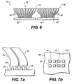
- Figs. 3a and 3b two tiles having edge structures according to two preferred embodiments of the method of the present invention is shown.
- the four edges of tile 10 are non-linear and the rows and columns of lightpipes have a stepped pattern such that each row or column 22 extends beyond the adjacent row or column on alternating ends to form an inter-digitated array 20 of lightpipes.
- the rows and columns on the opposing edges 24 and 26 of each tile have a complementary form such that the rows and columns on each tile edge can be inter-digitated as shown in Fig. 4 .
- Fig. 4 Referring to Fig.
- the tiles 10 are arranged to form a regular array of lightpipes 52 with the result that lightpipes at the edges of the tiles are inter-digitated to form an inter-digitated column 34 or row 36.
- This inter-digitation of the lightpipes at the tile edges has multiple benefits.
- the tile seam is less visible to the human eye because it is not straight, thus reducing the visibility of tile seams.
- the inter-digitation of lightpipes from two adjacent tiles obscures differences in uniformity between the tiles.
- the edges of the tiles can no longer slip with respect to each other because the stepped shape of the edge locks the tiles in position with respect to each other.
- the tiles are easier to assemble since they lock into a specific location with respect to each other.
- FIG. 3 and 4 show inter-digitation in two dimensions, it is also possible to inter-digitate in only one dimension, for example by rows only or by columns only. This approach provides alignment and visibility improvements in only one dimension but is significantly easier to manufacture.
- Applicants have conducted tests with human subjects simulating a tiled display device according to the present invention, on a CRT display that have shown that an inter-digitated edge between tiles increases by as much as fifty percent the threshold at which a global uniformity difference between the tiles is perceptible and reduces the visibility of an edge seam by as much as 50%.
- Each tile in a multi-tile device may have a complementary pattern on opposite edges 24 and 26 so that the tiles can be placed together with inter-digitated lightpipes along the edges. Tiles on the edges of a multi-tile device will not have a straight edge. The edges of the tiled array can be masked with a frame to obscure the non-linear external edges. Alternatively, special edge and corner tiles may be created with one or more conventional straight edges.
- each tile's information overlaps with the neighboring tiles so that neighboring tiles will have edge rows and edge columns of information in common.
- adjacent tiles overlap by one column or row 22 of pixel groups. This reduces the total number of rows and columns in the entire display by the total overlap amount.
- tile edge shapes may be used. Deeper stair steps that are multiple pixels deep may be used, as shown in Fig. 5 . Referring to Fig. 5 , the tiles incorporate a stair-step edge that overlaps by two columns or rows 44 of pixel groups. The process may be extended to larger overlaps with improved seam hiding and apparent tile uniformity but at the cost of more overlapped rows or columns.
- the tiles 10 include a flat-panel display 50 with a faceplate 54 comprising an array of lightpipes 52.
- Suitable flat-panel displays may be, for example, liquid crystal displays, organic light emitting diode displays, or plasma displays.
- the faceplates 54 have edges 14 that serve to align one faceplate 54 with another.
- Each faceplate 54 has two faces, an input face 55 and an output face 56.
- the lightpipes 52 have an input side 55 located in close proximity to the flat-panel display 50 that conducts light from the pixels with which the lightpipes are aligned through the body of the lightpipes to the output side 56 from which light is emitted to a viewer.
- the output side 56 of the faceplate 54 is larger than the input side 55, to accommodate non-light emitting areas on the peripheries of individual flat-panel displays 50.
- each individual lightpipe must either be separated by a greater distance on the output side 56 than the input side 55 or must be larger on the output side 56 than on the input side 55. This allows the faceplates 54 to be aligned along the output sides 56 while providing space for a flat-panel display 50 to be located in alignment on the input side 55.
- each lightpipe transmits the light from more than one pixel.
- each lightpipe is associated with four pixels arranged in a two-by-two array.
- the number of pixels associated with each lightpipe will vary depending on the desired resolution of the overall display, the resolution of the individual displays used in each tile, and the number of lightpipes in the overall display.
- each lightpipe transmits light from more than one pixel, the effective resolution of each tile is reduced.
- electronic devices capable of transforming a conventional video or other signal (for example, an HDTV or DVI signal) convert the input signal into a set of signals, each associated with one display tile.
- the converted signal is at a reduced resolution and transmits a single pixel element signal to all of the pixels associated with each lightpipe.
Landscapes
- Physics & Mathematics (AREA)
- Nonlinear Science (AREA)
- General Physics & Mathematics (AREA)
- Optics & Photonics (AREA)
- Engineering & Computer Science (AREA)
- Mathematical Physics (AREA)
- Chemical & Material Sciences (AREA)
- Crystallography & Structural Chemistry (AREA)
- Manufacturing & Machinery (AREA)
- Theoretical Computer Science (AREA)
- Devices For Indicating Variable Information By Combining Individual Elements (AREA)
- Light Guides In General And Applications Therefor (AREA)
Applications Claiming Priority (2)
| Application Number | Priority Date | Filing Date | Title |
|---|---|---|---|
| US10/785,624 US6999138B2 (en) | 2004-02-24 | 2004-02-24 | Tiled display comprising faceplate and displays with at least one defective pixel and method of manufacturing said tiled display |
| PCT/US2005/005999 WO2005083659A1 (en) | 2004-02-24 | 2005-02-24 | Tiled display |
Publications (2)
| Publication Number | Publication Date |
|---|---|
| EP1719098A1 EP1719098A1 (en) | 2006-11-08 |
| EP1719098B1 true EP1719098B1 (en) | 2008-12-24 |
Family
ID=34861655
Family Applications (1)
| Application Number | Title | Priority Date | Filing Date |
|---|---|---|---|
| EP05714051A Expired - Lifetime EP1719098B1 (en) | 2004-02-24 | 2005-02-24 | Tiled display |
Country Status (7)
| Country | Link |
|---|---|
| US (1) | US6999138B2 (https=) |
| EP (1) | EP1719098B1 (https=) |
| JP (1) | JP4971127B2 (https=) |
| KR (1) | KR101054122B1 (https=) |
| DE (1) | DE602005011932D1 (https=) |
| TW (1) | TW200538834A (https=) |
| WO (1) | WO2005083659A1 (https=) |
Families Citing this family (20)
| Publication number | Priority date | Publication date | Assignee | Title |
|---|---|---|---|---|
| KR101030537B1 (ko) * | 2004-06-30 | 2011-04-21 | 엘지디스플레이 주식회사 | 액정표시장치 및 그를 이용한 휘도 편차 보상방법 |
| US8837896B2 (en) * | 2008-08-12 | 2014-09-16 | Dish Network L.L.C. | Visual extender for portable devices |
| US9013102B1 (en) | 2009-05-23 | 2015-04-21 | Imaging Systems Technology, Inc. | Radiation detector with tiled substrates |
| CN102270411B (zh) * | 2011-01-17 | 2012-07-18 | 深圳市保千里电子有限公司 | 一种无缝拼接显示屏装置及其无缝拼接方法 |
| WO2013002712A1 (en) * | 2011-06-30 | 2013-01-03 | Shl Group Ab | Non-dark border and seamless video wall device |
| WO2013059489A1 (en) * | 2011-10-18 | 2013-04-25 | Reald Inc. | Electronic display tiling apparatus and propagation based method thereof |
| US9435939B2 (en) | 2012-08-02 | 2016-09-06 | Apple Inc. | Displays with coherent fiber bundles |
| US9274369B1 (en) * | 2012-10-30 | 2016-03-01 | Google Inc. | Seamless display with tapered fused fiber bundle overlay |
| CN103258481A (zh) * | 2013-05-28 | 2013-08-21 | 利亚德光电股份有限公司 | Led灯板组件 |
| US9709838B2 (en) * | 2014-03-26 | 2017-07-18 | Samsung Electronics Co., Ltd. | Tiled display and bezelless liquid crystal display apparatus |
| KR102133914B1 (ko) * | 2014-03-26 | 2020-07-14 | 삼성전자주식회사 | 타일드 디스플레이 및 무베젤 액정 디스플레이 장치 |
| JP7288427B2 (ja) * | 2017-07-11 | 2023-06-07 | コーニング インコーポレイテッド | タイル張り状ディスプレイとその製造方法 |
| TWI781241B (zh) | 2017-11-08 | 2022-10-21 | 美商康寧公司 | 用於組裝顯示區域的裝置及方法 |
| KR102565690B1 (ko) * | 2018-07-26 | 2023-08-10 | 삼성전자주식회사 | 전자 장치 및 그 제어 방법 |
| US11208237B1 (en) | 2020-09-17 | 2021-12-28 | Dwight Hendrickson | Container for selective display |
| CN113707035A (zh) * | 2021-10-29 | 2021-11-26 | 惠科股份有限公司 | 光学拼接结构及其制作方法和拼接显示装置 |
| KR102853019B1 (ko) * | 2021-11-12 | 2025-09-01 | 엘지디스플레이 주식회사 | 대면적 표시장치 및 대면적 표시장치 구동 시스템 |
| CN114137753B (zh) * | 2021-11-24 | 2022-11-25 | Tcl华星光电技术有限公司 | 一种显示模组及显示装置 |
| CN114187849B (zh) * | 2021-12-09 | 2024-03-15 | 惠州华星光电显示有限公司 | Led显示面板及显示设备 |
| CN114694519B (zh) * | 2022-04-24 | 2023-10-20 | 湖北长江新型显示产业创新中心有限公司 | 面板拼接系统和面板拼接方法 |
Family Cites Families (28)
| Publication number | Priority date | Publication date | Assignee | Title |
|---|---|---|---|---|
| US4299447A (en) * | 1979-06-27 | 1981-11-10 | The United States Of America As Represented By The Secretary Of The Navy | Liquid crystal fiber optics large screen display panel |
| JPS60203915A (ja) | 1984-03-28 | 1985-10-15 | Matsushita Electric Ind Co Ltd | 大型液晶デイスプレイ |
| US4695716A (en) * | 1985-12-13 | 1987-09-22 | Xerox Corporation | Image sensor array for assembly with like arrays to form a longer array |
| JPS63142330A (ja) | 1986-12-05 | 1988-06-14 | Alps Electric Co Ltd | 液晶表示装置 |
| JP2771060B2 (ja) * | 1990-11-09 | 1998-07-02 | シャープ株式会社 | 液晶表示装置 |
| CA2055142C (en) * | 1990-11-09 | 1995-03-28 | Atsushi Asada | Liquid crystal display apparatus |
| EP0491662B1 (en) | 1990-12-17 | 1996-05-15 | OIS Optical Imaging Systems, Inc. | Liquid crystal display having diverging/magnifying faceplate |
| CA2084103C (en) * | 1991-12-02 | 1999-07-27 | Keiji Sakai | A display apparatus |
| FR2687494B1 (fr) * | 1992-02-18 | 1996-10-25 | Thomson Tubes Electroniques | Ecran matriciel notamment de grandes dimensions et procede pour la realisation d'un tel ecran matriciel. |
| US5372927A (en) * | 1993-10-21 | 1994-12-13 | Eastman Kodak Company | Process for the low pag preparation of high aspect ratio tabular grain emulsions with reduced grain thicknesses |
| US6035013A (en) * | 1994-06-01 | 2000-03-07 | Simage O.Y. | Radiographic imaging devices, systems and methods |
| US5572034A (en) * | 1994-08-08 | 1996-11-05 | University Of Massachusetts Medical Center | Fiber optic plates for generating seamless images |
| TW347479B (en) * | 1994-12-15 | 1998-12-11 | Sharp Kk | Liquid crystal display panel and liquid crystal display apparatus |
| US5889568A (en) * | 1995-12-12 | 1999-03-30 | Rainbow Displays Inc. | Tiled flat panel displays |
| US5801797A (en) * | 1996-03-18 | 1998-09-01 | Kabushiki Kaisha Toshiba | Image display apparatus includes an opposite board sandwiched by array boards with end portions of the array boards being offset |
| US5903328A (en) * | 1997-06-16 | 1999-05-11 | Rainbow Displays, Inc. | Tiled flat-panel display with tile edges cut at an angle and tiles vertically shifted |
| US5908740A (en) * | 1997-11-21 | 1999-06-01 | Eastman Kodak Company | Process for preparing high chloride (100) tabular grain emulsions |
| JP4191276B2 (ja) * | 1998-01-09 | 2008-12-03 | 富士通株式会社 | 表示装置 |
| US6897855B1 (en) | 1998-02-17 | 2005-05-24 | Sarnoff Corporation | Tiled electronic display structure |
| US6370019B1 (en) * | 1998-02-17 | 2002-04-09 | Sarnoff Corporation | Sealing of large area display structures |
| US6259838B1 (en) * | 1998-10-16 | 2001-07-10 | Sarnoff Corporation | Linearly-addressed light-emitting fiber, and flat panel display employing same |
| US6498592B1 (en) * | 1999-02-16 | 2002-12-24 | Sarnoff Corp. | Display tile structure using organic light emitting materials |
| JP3595759B2 (ja) * | 1999-07-02 | 2004-12-02 | キヤノン株式会社 | 撮像装置および撮像システム |
| US6618115B1 (en) * | 1999-11-19 | 2003-09-09 | Semiconductor Energy Laboratory Co., Ltd. | Defective pixel compensation system and display device using the system |
| US6385430B1 (en) * | 2001-02-07 | 2002-05-07 | Xerox Corporation | Overlapping position sensors for object position tracking |
| JP2003332633A (ja) | 2002-05-16 | 2003-11-21 | Sony Corp | 表示装置および表示装置の製造方法 |
| US6881946B2 (en) | 2002-06-19 | 2005-04-19 | Eastman Kodak Company | Tiled electro-optic imaging device |
| US7031579B2 (en) * | 2002-06-26 | 2006-04-18 | L-3 Communications Corporation | High resolution display component, system and method |
-
2004
- 2004-02-24 US US10/785,624 patent/US6999138B2/en not_active Expired - Lifetime
-
2005
- 2005-02-23 TW TW094105329A patent/TW200538834A/zh unknown
- 2005-02-24 JP JP2007500988A patent/JP4971127B2/ja not_active Expired - Lifetime
- 2005-02-24 KR KR1020067017011A patent/KR101054122B1/ko not_active Expired - Lifetime
- 2005-02-24 EP EP05714051A patent/EP1719098B1/en not_active Expired - Lifetime
- 2005-02-24 WO PCT/US2005/005999 patent/WO2005083659A1/en not_active Ceased
- 2005-02-24 DE DE602005011932T patent/DE602005011932D1/de not_active Expired - Lifetime
Also Published As
| Publication number | Publication date |
|---|---|
| EP1719098A1 (en) | 2006-11-08 |
| KR20070001151A (ko) | 2007-01-03 |
| JP2007524133A (ja) | 2007-08-23 |
| WO2005083659A1 (en) | 2005-09-09 |
| DE602005011932D1 (de) | 2009-02-05 |
| US20050185114A1 (en) | 2005-08-25 |
| JP4971127B2 (ja) | 2012-07-11 |
| TW200538834A (en) | 2005-12-01 |
| KR101054122B1 (ko) | 2011-08-03 |
| US6999138B2 (en) | 2006-02-14 |
Similar Documents
| Publication | Publication Date | Title |
|---|---|---|
| EP1719098B1 (en) | Tiled display | |
| US6881946B2 (en) | Tiled electro-optic imaging device | |
| EP3909041B1 (en) | Display device including radiant heat blocking layer | |
| US11263933B2 (en) | LED panel and display apparatus having the same | |
| US7864136B2 (en) | Tiled electronic display structure | |
| KR101113538B1 (ko) | 터치 스크린 내장형 평판표시장치 및 그 구동방법 | |
| EP3093833B1 (en) | Double-sided display device | |
| KR20170013354A (ko) | 타일화된 디스플레이 패널들 사이의 기계적 분리의 마스킹 | |
| US20130176352A1 (en) | Display device | |
| EP2330627A2 (en) | Display Tile Structure using Organic Light Emitting Materials | |
| KR20210027628A (ko) | 표시 장치 및 표시 장치의 구동 방법 | |
| EP2498123A1 (en) | Display device | |
| KR20180034779A (ko) | 터치 구동 회로, 터치 스크린 내장형 유기발광표시장치와 그 구동 방법 | |
| US20210110782A1 (en) | Display Device and Driving Method Thereof | |
| US20060097957A1 (en) | Display panel and large display using such display panel | |
| KR20170006039A (ko) | 다중 시각 표시 장치 | |
| CN110376815B (zh) | 一种显示面板及显示装置 | |
| KR100752377B1 (ko) | 유기 전계발광 표시장치 | |
| EP3913612A1 (en) | Dual face display device | |
| KR20240120471A (ko) | 디스플레이 장치 및 이를 포함하는 멀티 스크린 디스플레이 장치 | |
| TR202007729A2 (tr) | Çi̇ft yüzlü görüntüleme ci̇hazi | |
| GB2390500A (en) | Composite image display |
Legal Events
| Date | Code | Title | Description |
|---|---|---|---|
| PUAI | Public reference made under article 153(3) epc to a published international application that has entered the european phase |
Free format text: ORIGINAL CODE: 0009012 |
|
| 17P | Request for examination filed |
Effective date: 20060713 |
|
| AK | Designated contracting states |
Kind code of ref document: A1 Designated state(s): DE FR GB |
|
| DAX | Request for extension of the european patent (deleted) | ||
| RBV | Designated contracting states (corrected) |
Designated state(s): DE FR GB |
|
| GRAP | Despatch of communication of intention to grant a patent |
Free format text: ORIGINAL CODE: EPIDOSNIGR1 |
|
| GRAS | Grant fee paid |
Free format text: ORIGINAL CODE: EPIDOSNIGR3 |
|
| GRAS | Grant fee paid |
Free format text: ORIGINAL CODE: EPIDOSNIGR3 |
|
| GRAA | (expected) grant |
Free format text: ORIGINAL CODE: 0009210 |
|
| AK | Designated contracting states |
Kind code of ref document: B1 Designated state(s): DE FR GB |
|
| REG | Reference to a national code |
Ref country code: GB Ref legal event code: FG4D |
|
| REF | Corresponds to: |
Ref document number: 602005011932 Country of ref document: DE Date of ref document: 20090205 Kind code of ref document: P |
|
| PLBE | No opposition filed within time limit |
Free format text: ORIGINAL CODE: 0009261 |
|
| STAA | Information on the status of an ep patent application or granted ep patent |
Free format text: STATUS: NO OPPOSITION FILED WITHIN TIME LIMIT |
|
| 26N | No opposition filed |
Effective date: 20090925 |
|
| PGFP | Annual fee paid to national office [announced via postgrant information from national office to epo] |
Ref country code: FR Payment date: 20120203 Year of fee payment: 8 |
|
| PGFP | Annual fee paid to national office [announced via postgrant information from national office to epo] |
Ref country code: DE Payment date: 20120229 Year of fee payment: 8 |
|
| PGFP | Annual fee paid to national office [announced via postgrant information from national office to epo] |
Ref country code: GB Payment date: 20120127 Year of fee payment: 8 |
|
| GBPC | Gb: european patent ceased through non-payment of renewal fee |
Effective date: 20130224 |
|
| REG | Reference to a national code |
Ref country code: FR Ref legal event code: ST Effective date: 20131031 |
|
| REG | Reference to a national code |
Ref country code: DE Ref legal event code: R119 Ref document number: 602005011932 Country of ref document: DE Effective date: 20130903 |
|
| PG25 | Lapsed in a contracting state [announced via postgrant information from national office to epo] |
Ref country code: FR Free format text: LAPSE BECAUSE OF NON-PAYMENT OF DUE FEES Effective date: 20130228 Ref country code: GB Free format text: LAPSE BECAUSE OF NON-PAYMENT OF DUE FEES Effective date: 20130224 Ref country code: DE Free format text: LAPSE BECAUSE OF NON-PAYMENT OF DUE FEES Effective date: 20130903 |