EP1715315B1 - Bolometrischer Detektor, Vorricthung zur Detektion elektromagnetischer Submillimeter- und Millimeterwellen mit einem solchen Detektor - Google Patents
Bolometrischer Detektor, Vorricthung zur Detektion elektromagnetischer Submillimeter- und Millimeterwellen mit einem solchen Detektor Download PDFInfo
- Publication number
- EP1715315B1 EP1715315B1 EP06300295A EP06300295A EP1715315B1 EP 1715315 B1 EP1715315 B1 EP 1715315B1 EP 06300295 A EP06300295 A EP 06300295A EP 06300295 A EP06300295 A EP 06300295A EP 1715315 B1 EP1715315 B1 EP 1715315B1
- Authority
- EP
- European Patent Office
- Prior art keywords
- detector
- electromagnetic radiation
- antenna
- bolometric
- receiving antenna
- Prior art date
- Legal status (The legal status is an assumption and is not a legal conclusion. Google has not performed a legal analysis and makes no representation as to the accuracy of the status listed.)
- Expired - Lifetime
Links
Images
Classifications
-
- G—PHYSICS
- G01—MEASURING; TESTING
- G01J—MEASUREMENT OF INTENSITY, VELOCITY, SPECTRAL CONTENT, POLARISATION, PHASE OR PULSE CHARACTERISTICS OF INFRARED, VISIBLE OR ULTRAVIOLET LIGHT; COLORIMETRY; RADIATION PYROMETRY
- G01J5/00—Radiation pyrometry, e.g. infrared or optical thermometry
- G01J5/10—Radiation pyrometry, e.g. infrared or optical thermometry using electric radiation detectors
- G01J5/20—Radiation pyrometry, e.g. infrared or optical thermometry using electric radiation detectors using resistors, thermistors or semiconductors sensitive to radiation, e.g. photoconductive devices
-
- G—PHYSICS
- G01—MEASURING; TESTING
- G01J—MEASUREMENT OF INTENSITY, VELOCITY, SPECTRAL CONTENT, POLARISATION, PHASE OR PULSE CHARACTERISTICS OF INFRARED, VISIBLE OR ULTRAVIOLET LIGHT; COLORIMETRY; RADIATION PYROMETRY
- G01J5/00—Radiation pyrometry, e.g. infrared or optical thermometry
- G01J5/02—Constructional details
- G01J5/08—Optical arrangements
- G01J5/0837—Microantennas, e.g. bow-tie
-
- H—ELECTRICITY
- H01—ELECTRIC ELEMENTS
- H01Q—ANTENNAS, i.e. RADIO AERIALS
- H01Q1/00—Details of, or arrangements associated with, antennas
- H01Q1/36—Structural form of radiating elements, e.g. cone, spiral, umbrella; Particular materials used therewith
- H01Q1/38—Structural form of radiating elements, e.g. cone, spiral, umbrella; Particular materials used therewith formed by a conductive layer on an insulating support
-
- H—ELECTRICITY
- H01—ELECTRIC ELEMENTS
- H01Q—ANTENNAS, i.e. RADIO AERIALS
- H01Q1/00—Details of, or arrangements associated with, antennas
- H01Q1/44—Details of, or arrangements associated with, antennas using equipment having another main function to serve additionally as an antenna, e.g. means for giving an antenna an aesthetic aspect
-
- G—PHYSICS
- G01—MEASURING; TESTING
- G01J—MEASUREMENT OF INTENSITY, VELOCITY, SPECTRAL CONTENT, POLARISATION, PHASE OR PULSE CHARACTERISTICS OF INFRARED, VISIBLE OR ULTRAVIOLET LIGHT; COLORIMETRY; RADIATION PYROMETRY
- G01J1/00—Photometry, e.g. photographic exposure meter
- G01J1/02—Details
- G01J1/0252—Constructional arrangements for compensating for fluctuations caused by, e.g. temperature, or using cooling or temperature stabilization of parts of the device; Controlling the atmosphere inside a photometer; Purge systems, cleaning devices
Definitions
- the present invention relates to a bolometric detector, as well as a device for detecting electromagnetic waves, in particular located in the millimeter and submillimeter wave field using such a detector.
- millimeter waves and more particularly submillimetric waves presents a certain number of interests, in particular on the scientific and technological level.
- this range of wavelengths corresponds to many excitations in matter (phonons, rotation of molecules, intraband transition, ).
- the detection of these waves and their interpretation have many applications, particularly in the field of the analysis of pollutants of the atmosphere, in biophysics, because of the absorption of these waves by the liquids, but also in telecommunications , in radio astronomy, collision avoidance radar, biomedical imaging, etc ...
- the first of these consists in detecting the electromagnetic waves by means of an antenna so as to create an electrical signal, the processing of which is carried out by an electronic circuit operating at the frequency of the wave.
- the disadvantage of detectors operating according to this first principle is to be strongly limited in frequencies.
- the second known technical principle is to implement an electromagnetic wave detection antenna, capable of creating a heat flow, the measurement of which corresponds to the desired signal.
- the detectors used in the context of this principle are traditionally constituted by the family of bolometric detectors.
- the thermal detectors to which family the bolometric detectors belong, absorb the power of an incident electromagnetic radiation, convert it into heat, which is then transformed into a signal resulting from the correlative temperature rise with respect to a reference temperature in a determined range for associating with these temperature variations electrical signals corresponding to the actual measurement of the incident electromagnetic flux. It is conceivable, however, that when a temperature variation is measured, said detector must be as thermally isolated as possible so that the measurement is not polluted by the interference of the constituents to which it is mechanically and electrically connected. .
- thermoelectric for thermocouples Under the effect of the incident radiation, the detector heats up and transmits the correlative temperature rise to the sensitive thermal material.
- This increase in temperature causes a variation of a property of said sensitive material, such as an appearance of electric charges by pyroelectric effect, the variation of the capacitance by changing the dielectric constant for the capacitive detectors, the variation of the effect voltage.
- thermoelectric for thermocouples and the variation of resistance for bolometric detectors.
- bolometric detectors In the field of infrared detection, the use of bolometric detectors is widespread. These detectors are conventionally constituted by a suspended membrane, which comprises a thin layer (typically between 0.1 and 1 micrometer) made of a temperature-sensitive bolometric material, two so-called coplanar electrodes and an absorber, whose function is to capture electromagnetic radiation. to convert it into heat within the structure.
- the membrane is suspended above the support substrate, via anchoring points or fixing pins, adapted to isolate said membrane from the substrate.
- These structures, also called pillars can bring the excitation potentials or stimuli to the conductive parts or electrodes of the bolometric detector via flat and elongated structures, also called isolation arms. They are therefore electrically conductive but on the other hand have the highest possible thermal resistance.
- the bolometric material that is to say the sensitive material must have a low heat mass, must be well insulated thermally relative to the support, and finally must have a high sensitivity to the effect of converting the heating into an electrical signal.
- the support substrate receives a read circuit constituted by an electronic circuit integrating means of sequential addressing or multiplexing of the elementary detectors and electrical excitation means (stimuli) and of pre-processing the electrical signals generated by said elementary detectors.
- a read circuit constituted by an electronic circuit integrating means of sequential addressing or multiplexing of the elementary detectors and electrical excitation means (stimuli) and of pre-processing the electrical signals generated by said elementary detectors.
- a read circuit makes it possible to serialize the signals coming from the different elementary detectors and to transmit them to a small number of outputs, in order to be exploited by a usual imaging system, such as for example an infrared camera.
- these detectors are encapsulated under vacuum or under low pressure of inert gas conducting heat within a housing, then provided with a transparent window to the length of the band. concerned wave.
- the bolometric material used consists of polycrystalline or amorphous silicon of p-type or n weakly or strongly resistive, but can also be made of vanadium oxide (V 2 O 5 , VO 2 ) or a cuprate (YBaCuO ) developed in a semiconductor phase.
- V 2 O 5 , VO 2 vanadium oxide
- YBaCuO cuprate
- thermometric detectors have been widely described in relation to detection in the infrared domain. For this wavelength range, it is possible to simultaneously combine the thermometric and absorption functions of the incident infrared radiation on the bolometric plate.
- an electromagnetic detection system must have dimensions close to the order of magnitude of the wavelength considered in order to be effective.
- the collected power proportional to the surface of the detector
- the spatial resolution limits the spatial resolution to a value of the order of the wavelength in the dimensions of the plane.
- the optimal dimensions for a detector are therefore of this order of magnitude.
- the absorber that is to say the membrane supporting the bolometric sensitive element provides both the electromagnetic coupling function with the incident radiation, and therefore the absorption of said radiation, and the conversion function of this radiation. heat flux radiation by Joule effect.
- the first of these two functions is performed by means of a receiving antenna, and the second function is provided by a resistive load associated with the antenna.
- Such bolometric detection devices known as “antenna” are known, capable of operating at temperatures ranging from 150 to 300 K, therefore at ambient temperature. These devices implement arrays or matrices of such detectors.
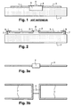
- thermometer (4) It basically consists of an antenna (1) consisting of a conductive layer deposited on a non-conductive substrate (2). It comprises a resistive metal (3) constituting both the resistive load of the antenna, suitable for generating the heating power, and the insulating arms of a thermometer or bolometer (4), composed of a thermo-magnetic material. resistive, such as for example amorphous silicon or vanadium oxide. As can be seen, it is defined under the thermometer (4) a cavity (5) for thermal insulation thereof.
- the electric currents generated in the antenna (1) by the incident radiation are dissipated in the insulation arms (3) by joule effect.
- a reflective metal plane optimizes the absorption for a given range of wavelengths.
- This reflector is generally positioned at a distance equal to n times ⁇ / 4 of the antenna, n being an integer.
- the electrical connection between the antenna and the thermometer is necessarily accompanied by a thermal link, which significantly impairs the performance of the bolometers, since they also measure a variation in temperature with respect to a value. reference.
- the described “ Bow-Tie " type antenna (bow tie) is placed above a metal plane at a distance equal to one quarter of the detector's operating wavelength, thus defining a so-called cavity " quarter wave , well known in itself.
- the resistive load is constituted by the load resistance of the antenna.
- the thermometer consists of a monocrystalline silicon junction diode, whose thermal insulation results from the etching on the back of the substrate made of silicon.
- the antenna of particular shape is deposited on a layer of silicon oxide SiO, which because of the technology employed (thin film type) has a thickness e of the order of one micron.
- a " Bow-Tie " type antenna, optimized for a detector around a frequency of 1 THz has a surface S of the order of 300 x 300 ⁇ m 2 , about the square of the wavelength of use.
- the antenna is, in this case, almost the thermal mass; in other words, it is not thermally insulated, and because of its mechanical and electrical connection with the thermometer, it is not thermally insulated satisfactorily.
- the antenna is not thermally insulated, only the constituent thermo-resistive material of the thermometer, is actually thermally isolated from the substrate, but not the antenna.
- thermometer or bolometer there is therefore no satisfactory technical solution to achieve a relatively simple way in terms of technology, a complete or almost complete thermal insulation of the thermometer or bolometer.
- the invention proposes a solution to these various technical problems, obviously in the field of the detection of millimetric and submillimetric electromagnetic waves.
- the general principle underlying the present invention is based on the thermal insulation of the antenna with respect to the substrate.
- the problem of thermal insulation between the thermometer and the antenna does not arise then, and the thermal insulation of the assembly becoming independent of electromagnetic considerations.
- the invention firstly aims at a bolometric detector of electromagnetic radiation, in particular at frequencies between 100 GHz and 10 THz, according to claim 1.
- the receiving antenna is itself isolated from the substrate-support, the latter being connected only very indirectly to said substrate and in particular not at its main faces.
- thermometric element the assembly constituted by the antenna, the thermometric element and the resistive loads, since as well, the only remaining contact intervenes only at the level , in particular free edges of the antenna, that is to say opposite to the thermometric element.
- the assembly thus defined is held suspended above the substrate advantageously by means of isolation arms, electrically conductive but thermally insulating conductors, themselves resting on anchor points formed on said substrate, and secured at the free edges of the antenna.
- the antennas used may be of the dipole type, that is to say extend on either side of the thermometric element, or of the double dipole type, that is to say provided with two outputs on the each of their connection zones to the thermometric element.
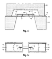
- the elementary detector of the invention has an assembly consisting of the receiving antenna (1), the bolometer (4) and a load resistor (3), suspended above the substrate (2), by means of arms insulation (6), resting on pillars (7) provided for this purpose on said substrate.
- insulating arms (6) are thermally insulating, so that the assembly thus defined is itself thermally isolated from the substrate, which constitutes one of the essential aims of the invention.
- these arms (6) are electrically conductive, so as to allow the delivery of stimuli at the bolometer (4), and the collection of electrical signals generated by the latter, following irradiation of the detector by electromagnetic radiation in the determined wavelength range.
- the detector described in relation to Figures 2 and 3a is equipped with a dipole antenna.
- the antenna can be of the double dipole type (1 '). In doing so, there is a small electrically conductive surface, making it possible to minimize the heat capacity and the radiation losses of the assembly.
- the radiation losses will be low in all cases, because the conductive layers used for the antenna have almost zero emissivities in the infrared (and indeed in almost the entire spectrum from the visible range into the field millimeter) because of the intrinsic characteristics of the materials used.
- the absorption band obtained at -3dB with such a detector is about 1 THz.
- a band centered on 650 GHz or 850 GHz can also be obtained using appropriate filters, such as networks of slots positioned in front of the detector.
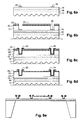
- thermometer 10
- dipole antenna or double dipole antenna 11, 11 '
- anchoring points (12) formed on the one hand, in the vicinity of the edges free of the antenna, and secondly, in the immediate vicinity of the thermometer.
- the assembly is again thermally insulated from the substrate (2) by isolation arms (13).
- isolation arms 13
- These are composed either of a single dielectric layer (13) made of silicon oxide SiO or of silicon nitride SiN, or of a dielectric layer surmounted by a resistive layer, for example made of titanium nitride TiN ( 14), to ensure the routing of stimuli at the thermometer.
- the substrate is an SOI substrate, composed of a silicon layer (15) with a thickness between 1 and 20 ⁇ m, of a buried oxide layer (for example SiO) (16) with a thickness of between 3000 Angstroms. and 2 ⁇ m, and a solid substrate (17), which is generally 400 to 500 ⁇ m thick.
- SOI substrate composed of a silicon layer (15) with a thickness between 1 and 20 ⁇ m, of a buried oxide layer (for example SiO) (16) with a thickness of between 3000 Angstroms. and 2 ⁇ m, and a solid substrate (17), which is generally 400 to 500 ⁇ m thick.
- the assembly is integrated in a substrate (18), etched to a thickness equal to ⁇ / 4 where ⁇ is the wavelength of use of the detector, and whose background of the etching is advantageously covered with a conductive layer (19), adapted to act as a reflector.
- This configuration allows the encapsulation of the detector and then imposes a lighting from the rear face.
- the possible doping of these layers is carried out by introducing a doping gas (BF3, PH3, etc.) into the reactor or by ion implantation.
- a doping gas BF3, PH3, etc.
- the etching of these materials is generally performed by plasma etching methods.
- the metallic materials (Ti, TiN, Pt, Al, Pd, Ni, NiCr, etc.) constituting the resistive elements, the electrodes and the various metallizations such as the interconnection lines, the antennas or the antenna load resistance, are also deposited by sputtering, or by thermal decomposition (LPCVD) or plasma (PECVD). These metallizations are defined by chemical etching or plasma etching processes or by a process known in the English term as "lift off”. The thickness of these layers is between 0.005 ⁇ m and 1 ⁇ m.
- the conductive lines and the metal connection pads (20), for example made of aluminum, on which the holding pillars will be manufactured, are produced by deposition, photolithography and etching. These deposits are made on a stack consisting of silicon (15), the buried layer of silicon oxide (116), and the bulk substrate (17).
- One or more metal layers (23, 24), at least one of which is highly conductive (Al, Au) are deposited on the insulating membrane (22), and are intended to form on the one hand the antenna, and on the other hand the polarization electrodes of the thermometer and the load resistance of the antenna (in resistive metal: TiN, TaN ). The whole is engraved through a resin mask (see Figure 6b ).
- one or more metal layers (25) intended to constitute the base of the electrical contacts between the thermometer and the interconnection lines, and for example made of titanium or titanium nitride TiN are deposited and etched ( Figure 6c ).
- a first conductive layer (25) is etched to form the antenna. In the same way, such a conductive layer (25) is etched to form the contact electrodes (see FIG. Figure 6d ).
- the heat-resistive material (6) made of amorphous silicon or vanadium oxide, for example, is deposited and etched through a resin mask that protects the thermometric zone.
- the substrate is then etched by a BOSH plasma-assisted chemical etching (see Figure 6e ).
- the last step is to release structures by etching the sacrificial layer.
- the hood can be etched by wet chemistry. Before depositing it or sticking it under vacuum on the front face (like the embodiment described in connection with the figure 4 , a conductive layer (Al, Au) thick about 1 micron, preceded by a bonding layer (for example titanium) is deposited by sputtering.
- a conductive layer Al, Au
- a bonding layer for example titanium
Landscapes
- Physics & Mathematics (AREA)
- General Physics & Mathematics (AREA)
- Spectroscopy & Molecular Physics (AREA)
- Photometry And Measurement Of Optical Pulse Characteristics (AREA)
- Radiation Pyrometers (AREA)
- Support Of Aerials (AREA)
- Medicines Containing Antibodies Or Antigens For Use As Internal Diagnostic Agents (AREA)
- Details Of Aerials (AREA)
- Aiming, Guidance, Guns With A Light Source, Armor, Camouflage, And Targets (AREA)
- Geophysics And Detection Of Objects (AREA)
- Nuclear Medicine (AREA)
- Measurement Of The Respiration, Hearing Ability, Form, And Blood Characteristics Of Living Organisms (AREA)
Claims (8)
- Bolometrischer Detektor für eine elektromagnetische Strahlung, umfassend:- eine Empfangsatenne (1, 1', 11'), die dazu bestimmt ist, die elektromagnetische Strahlung zu sammeln und auf diese Weise die elektromagnetische Kopplung zu gewährleisten;- eine resistive Last (3), die in der Lage ist, die gesammelte elektromagnetische Leistung in Wärmeleistung zu überführen;- ein thermometrisches Element (4), das mit der Empfangsantenne über die resistive Last verbunden ist und von einem Trägersubstrat (2) thermisch isoliert ist, das in der Lage ist, eine elektronische Schaltung aufzunehmen, in die Mittel zur elektrischen Anregung und Vorbehandlung der durch den Detektor erzeugten elektrischen Signale integriert sind;bei dem:die Empfangsantenne ihrerseits vom Trägersubstrat (2) thermisch isoliert ist,die aus der Empfangsantenne (1, 1', 11'), der resistiven Last (3) und dem thermometrischen Element (4) bestehende Einheit oberhalb des Trägersubstrats über thermisch isolierende Isolationsarme (6, 13, 14) aufgehängt ist, die ihrerseits auf Verankerungspunkten (7, 12) aufliegen, die auf dem Trägersubstrat vorgesehen sind, wobei mindestens ein Teil (6, 13) der Isolationsarme (6, 13) auf Höhe des freien Rands der Hauptseiten der Empfangsatenne verbunden ist.
- Bolometrischer Detektor für eine elektromagnetische Strahlung nach Anspruch 1, bei dem die Empfangsantenne (11') auch mit den Isolationsarmen (14) in Nähe des thermometrischen Elements (4) verbunden ist.
- Bolometrischer Detektor für eine elektromagnetische Strahlung nach einem der Ansprüche 1 und 2, bei dem die Isolationsarme (6, 14) elektrische Leiter sind.
- Bolometrischer Detektor für eine elektromagnetische Srahlung nach einem der Ansprüche 1 bis 3, bei dem die Empfangsantenne vom Typ Dipol oder Doppeldipol ist.
- Bolometrischer Detektor für eine elektromagnetische Strahlung nach einem der Ansprüche 1 bis 4, bei dem das thermometrische Element (4) aus einem bolometrischen Werkstoff hergestellt ist, der aus der Gruppe ausgewählt ist, die polykristallines oder amorphes Silicium vom Typ p oder n, die Vanadiumoxide V2O5 oder VO2 und die in einer halbleitenden Phase abgeschiedenen Cuprate YBaCuO umfasst.
- Bolometrischer Detektor für eine elektromagnetische Strahlung nach einem der Ansprüche 1 bis 5, der im Frequenzbereich zwischen 100 GHz und 10 THz arbeitet.
- Vorrichtung zum Erfassen einer elektromagnetischen Strahlung, dadurch gekennzeichnet, dass sie aus einer eindimensionalen oder zweidimensionalen Matrix von bolometrischen Einzeldetektoren besteht, die mit einem Lesekreis elektrisch verbunden sind und den Merkmalen der Ansprüche 1 bis 6 entsprechen.
- Vorrichtung zum Erfassen einer elektromagnetischen Strahlung nach Anspruch 7, die im Frequenzbereich zwischen 100 GHz und 10 THz arbeitet.
Applications Claiming Priority (1)
| Application Number | Priority Date | Filing Date | Title |
|---|---|---|---|
| FR0503836A FR2884608B1 (fr) | 2005-04-18 | 2005-04-18 | Detecteur bolometrique, dispositif de detection d'ondes electromagnetiques submillimetriques et millimetriques mettant en oeuvre un tel detecteur |
Publications (2)
| Publication Number | Publication Date |
|---|---|
| EP1715315A1 EP1715315A1 (de) | 2006-10-25 |
| EP1715315B1 true EP1715315B1 (de) | 2010-06-23 |
Family
ID=35266742
Family Applications (1)
| Application Number | Title | Priority Date | Filing Date |
|---|---|---|---|
| EP06300295A Expired - Lifetime EP1715315B1 (de) | 2005-04-18 | 2006-03-28 | Bolometrischer Detektor, Vorricthung zur Detektion elektromagnetischer Submillimeter- und Millimeterwellen mit einem solchen Detektor |
Country Status (6)
| Country | Link |
|---|---|
| US (1) | US7442934B2 (de) |
| EP (1) | EP1715315B1 (de) |
| JP (1) | JP5241077B2 (de) |
| AT (1) | ATE472098T1 (de) |
| DE (1) | DE602006015014D1 (de) |
| FR (1) | FR2884608B1 (de) |
Families Citing this family (24)
| Publication number | Priority date | Publication date | Assignee | Title |
|---|---|---|---|---|
| GB2392779B (en) * | 2002-09-04 | 2005-05-04 | Teraview Ltd | An Emitter |
| FI20065776A0 (sv) * | 2006-12-05 | 2006-12-05 | Pekka Neittaanmaeki | Förfarande för kontroll av värmekonduktivitet hos dielektriska nanofibrer och motsvarande anordning |
| FR2934044B1 (fr) * | 2008-07-17 | 2014-08-15 | Commissariat Energie Atomique | Detecteur bolometrique d'ondes electromagnetiques. |
| US8354642B2 (en) * | 2010-10-13 | 2013-01-15 | International Business Machines Corporation | Monolithic passive THz detector with energy concentration on sub-pixel suspended MEMS thermal sensor |
| JP5428783B2 (ja) * | 2009-11-12 | 2014-02-26 | 日本電気株式会社 | ボロメータ型THz波検出器 |
| JP2011237312A (ja) * | 2010-05-12 | 2011-11-24 | Hamamatsu Photonics Kk | テラヘルツ波検出器及びその製造方法 |
| US8570224B2 (en) * | 2010-05-12 | 2013-10-29 | Qualcomm Incorporated | Apparatus providing thermal management for radio frequency devices |
| FR2983953B1 (fr) | 2011-12-09 | 2014-01-03 | Commissariat Energie Atomique | Detecteur bolometrique d'un rayonnement electromagnetique dans le domaine du terahertz et dispositif de detection matriciel comportant de tels detecteurs |
| FR2983952B1 (fr) | 2011-12-09 | 2013-11-15 | Commissariat Energie Atomique | Detecteur bolometrique d'un rayonnement electromagnetique dans le domaine du terahertz |
| RU2511275C2 (ru) * | 2012-07-16 | 2014-04-10 | Федеральное государственное унитарное предприятие "Научно-исследовательский институт физических проблем им. Ф.В. Лукина" | Наноструктурный ик-приемник (болометр) с большой поверхностью поглощения |
| GB2507306A (en) * | 2012-10-25 | 2014-04-30 | Ibm | An antenna-coupled bolometer device for sensing electromagnetic radiation |
| US20140117237A1 (en) | 2012-10-30 | 2014-05-01 | International Business Machines Corporation | High responsivity device for thermal sensing in a terahertz radiation detector |
| US8957379B2 (en) | 2012-10-30 | 2015-02-17 | International Business Machines Corporation | Suspended wideband planar skirt antenna having low thermal mass for detection of terahertz radiation |
| US9052234B2 (en) | 2012-10-30 | 2015-06-09 | International Business Machines Corporation | Dipole antenna with reflectors having low thermal mass for detection of Terahertz radiation |
| US9759693B2 (en) | 2012-12-20 | 2017-09-12 | International Business Machines Corporation | Method of simulating the absorption of plane waves using FEM software tools |
| GB2513170B (en) * | 2013-04-18 | 2020-07-08 | Univ Of Ljubljana | Bolometric detection system with reflecting cavity |
| FR3009865B1 (fr) * | 2013-08-22 | 2015-07-31 | Commissariat Energie Atomique | Detecteur bolometrique a bolometre de compensation a thermalisation renforcee |
| US20150241281A1 (en) * | 2014-02-27 | 2015-08-27 | International Business Machines Corporation | Bolometer device for sensing electromagnetic radiation |
| JP6486695B2 (ja) * | 2015-01-14 | 2019-03-20 | 浜松ホトニクス株式会社 | ボロメータ型THz検出器 |
| CN105371966B (zh) * | 2015-11-13 | 2019-01-11 | 南方科技大学 | 一种新型辐射热测量计及制造方法 |
| CN111224232B (zh) * | 2018-11-23 | 2022-10-18 | 比亚迪股份有限公司 | 双频段全向天线及列车 |
| US12345575B2 (en) * | 2021-05-11 | 2025-07-01 | America as represented by the Secretary of the Army | Phonon disruptors for increased thermal resistance without sacrificing electrical signal quality in thermal sensors |
| US12320707B2 (en) * | 2021-05-11 | 2025-06-03 | The United States Of America As Represented By The Secretary Of The Army | Phonon disruptors for increased thermal resistance without sacrificing electrical signal quality in thermal sensors using alloy and intermetallic materials |
| CN117637898A (zh) * | 2022-08-09 | 2024-03-01 | 合肥工业大学 | 一种三维立体结构长波红外-太赫兹探测器及其制备方法 |
Family Cites Families (9)
| Publication number | Priority date | Publication date | Assignee | Title |
|---|---|---|---|---|
| JPH0627170A (ja) * | 1992-07-08 | 1994-02-04 | Sanyo Electric Co Ltd | 超電導電磁波検出素子 |
| AU1408497A (en) * | 1995-12-04 | 1997-06-27 | Lockheed-Martin Ir Imaging Systems, Inc. | Infrared radiation detector having a reduced active area |
| FI107407B (fi) * | 1997-09-16 | 2001-07-31 | Metorex Internat Oy | Alimillimetriaalloilla toimiva kuvausjärjestelmä |
| US6329655B1 (en) * | 1998-10-07 | 2001-12-11 | Raytheon Company | Architecture and method of coupling electromagnetic energy to thermal detectors |
| FR2788129B1 (fr) | 1998-12-30 | 2001-02-16 | Commissariat Energie Atomique | Detecteur bolometrique a antenne |
| US6292140B1 (en) * | 1999-11-03 | 2001-09-18 | Hypres, Inc. | Antenna for millimeter-wave imaging and bolometer employing the antenna |
| FR2845157B1 (fr) * | 2002-10-01 | 2004-11-05 | Commissariat Energie Atomique | Detecteur bolometrique a antenne comportant un interrupteur et dispositif d'imagerie le comportant. |
| FR2855609B1 (fr) * | 2003-05-26 | 2005-07-01 | Commissariat Energie Atomique | Dispositif de detection bolometrique a antenne, a cavite optimisee, pour ondes electromagnetiques millimetriques ou submillimetriques, et procede de fabrication de ce dispositif |
| WO2006039571A2 (en) * | 2004-10-01 | 2006-04-13 | Northrop Grumman Corporation | Focal plane antenna to sensor interface for an ultra-sensitive bolometer based sensor |
-
2005
- 2005-04-18 FR FR0503836A patent/FR2884608B1/fr not_active Expired - Fee Related
-
2006
- 2006-03-28 DE DE602006015014T patent/DE602006015014D1/de not_active Expired - Lifetime
- 2006-03-28 EP EP06300295A patent/EP1715315B1/de not_active Expired - Lifetime
- 2006-03-28 AT AT06300295T patent/ATE472098T1/de not_active IP Right Cessation
- 2006-03-30 US US11/393,973 patent/US7442934B2/en not_active Expired - Fee Related
- 2006-03-30 JP JP2006095481A patent/JP5241077B2/ja not_active Expired - Fee Related
Also Published As
| Publication number | Publication date |
|---|---|
| ATE472098T1 (de) | 2010-07-15 |
| FR2884608B1 (fr) | 2007-05-25 |
| DE602006015014D1 (de) | 2010-08-05 |
| US20060231761A1 (en) | 2006-10-19 |
| JP2006304290A (ja) | 2006-11-02 |
| FR2884608A1 (fr) | 2006-10-20 |
| EP1715315A1 (de) | 2006-10-25 |
| US7442934B2 (en) | 2008-10-28 |
| JP5241077B2 (ja) | 2013-07-17 |
Similar Documents
| Publication | Publication Date | Title |
|---|---|---|
| EP1715315B1 (de) | Bolometrischer Detektor, Vorricthung zur Detektion elektromagnetischer Submillimeter- und Millimeterwellen mit einem solchen Detektor | |
| EP2246677B1 (de) | Bolometrischer Detektor für elektromagnetische Strahlung im Spektralbereich von Infrarot bis Terahertz und Detektoranordnung mit solchen Detektoren. | |
| EP2602598B1 (de) | Bolometrischer Detektor für elektromagnetische Strahlung im Spektralbereich von Terahertz und Matrix, die solche Detektoren umfasst | |
| EP2340422A1 (de) | Bolometrischer detektor zum detektieren von elektromagnetischen welllen | |
| EP2700922B1 (de) | Bolometrischer Detektor einer elektromagnetischen Strahlung im Terahertzbereich, und Vorrichtung zur Matrixerkennung, die mit solchen Detektoren ausgestattet ist | |
| EP0971219B1 (de) | Thermischer Detektor mit Verstärkung durch bolometrischen Effekt | |
| EP0828145B1 (de) | Infrarot-Detektor und Verfahren zu dessen Herstellung | |
| WO2004025694A2 (fr) | Dispositif detecteur de rayonnement electromagnetique avec boitier integre comportant deux detecteurs superposes | |
| FR2735574A1 (fr) | Dispositif de detection bolometrique pour ondes millimetriques et submillimetriques et procede de fabrication de ce dispositif | |
| EP1482289B1 (de) | Bolometrisches Detetektionsverfahren für (Sub-)Millimeterwellen anhand eines antennengekoppelten Bolometers mit einem Hohlraum | |
| CA2959650A1 (fr) | Capteur de motifs thermiques a bolometres sous capsule(s) | |
| EP1880176B1 (de) | Thermischer detektor für elektromagnetische strahlung in einer die detektoren verwendenden infrarot-detektionseinrichtung | |
| EP2602599A1 (de) | Bolometrischer Detektor zur Erfassung von Teraherz-Strahlung | |
| EP2715296A1 (de) | Spektroskopischer detektor und entsprechendes verfahren | |
| EP2902758A1 (de) | Detektor für Photonenstrahlung, der ein Antennennetz und eine widerstandsfähige Spiralhalterung umfasst | |
| WO2019229353A1 (fr) | Systeme de detection a pixel sensible comportant un detecteur thermique et un dispositif de compensation | |
| FR2885690A1 (fr) | Detecteur thermique de rayonnements electromagnetiques et dispositif de detection infrarouge mettant en oeuvre de tels detecteurs | |
| FR3066017B1 (fr) | Dispositif pyroelectrique de detection infrarouge comportant un emetteur infrarouge de modulation | |
| WO2019043312A1 (fr) | Detecteur de rayonnement electromagnetique | |
| Gawarikar et al. | High detectivity uncooled thermopile detectors with spectrally selective responsivity | |
| EP1750107B1 (de) | Wärmedetektor für elektromagnetische Strahlung mit ausgerichteten Isolationselementen und Erfassungsvorrichtung zur Ingangsetzung solcher Detektoren | |
| FR3004001A1 (fr) | Detecteur d'ondes electromagnetiques avec proprietes ameliorees de selection de longueur d'onde |
Legal Events
| Date | Code | Title | Description |
|---|---|---|---|
| PUAI | Public reference made under article 153(3) epc to a published international application that has entered the european phase |
Free format text: ORIGINAL CODE: 0009012 |
|
| 17P | Request for examination filed |
Effective date: 20060823 |
|
| AK | Designated contracting states |
Kind code of ref document: A1 Designated state(s): AT BE BG CH CY CZ DE DK EE ES FI FR GB GR HU IE IS IT LI LT LU LV MC NL PL PT RO SE SI SK TR |
|
| AX | Request for extension of the european patent |
Extension state: AL BA HR MK YU |
|
| AKX | Designation fees paid |
Designated state(s): AT BE BG CH CY CZ DE DK EE ES FI FR GB GR HU IE IS IT LI LT LU LV MC NL PL PT RO SE SI SK TR |
|
| 17Q | First examination report despatched |
Effective date: 20070713 |
|
| APBK | Appeal reference recorded |
Free format text: ORIGINAL CODE: EPIDOSNREFNE |
|
| APBN | Date of receipt of notice of appeal recorded |
Free format text: ORIGINAL CODE: EPIDOSNNOA2E |
|
| APBR | Date of receipt of statement of grounds of appeal recorded |
Free format text: ORIGINAL CODE: EPIDOSNNOA3E |
|
| APAF | Appeal reference modified |
Free format text: ORIGINAL CODE: EPIDOSCREFNE |
|
| APBT | Appeal procedure closed |
Free format text: ORIGINAL CODE: EPIDOSNNOA9E |
|
| GRAP | Despatch of communication of intention to grant a patent |
Free format text: ORIGINAL CODE: EPIDOSNIGR1 |
|
| GRAS | Grant fee paid |
Free format text: ORIGINAL CODE: EPIDOSNIGR3 |
|
| RAP1 | Party data changed (applicant data changed or rights of an application transferred) |
Owner name: COMMISSARIAT A L'ENERGIE ATOMIQUE ET AUX ENERGIES |
|
| GRAA | (expected) grant |
Free format text: ORIGINAL CODE: 0009210 |
|
| AK | Designated contracting states |
Kind code of ref document: B1 Designated state(s): AT BE BG CH CY CZ DE DK EE ES FI FR GB GR HU IE IS IT LI LT LU LV MC NL PL PT RO SE SI SK TR |
|
| REG | Reference to a national code |
Ref country code: CH Ref legal event code: EP |
|
| REG | Reference to a national code |
Ref country code: IE Ref legal event code: FG4D Free format text: LANGUAGE OF EP DOCUMENT: FRENCH |
|
| REF | Corresponds to: |
Ref document number: 602006015014 Country of ref document: DE Date of ref document: 20100805 Kind code of ref document: P |
|
| REG | Reference to a national code |
Ref country code: NL Ref legal event code: VDEP Effective date: 20100623 |
|
| PG25 | Lapsed in a contracting state [announced via postgrant information from national office to epo] |
Ref country code: SE Free format text: LAPSE BECAUSE OF FAILURE TO SUBMIT A TRANSLATION OF THE DESCRIPTION OR TO PAY THE FEE WITHIN THE PRESCRIBED TIME-LIMIT Effective date: 20100623 Ref country code: LT Free format text: LAPSE BECAUSE OF FAILURE TO SUBMIT A TRANSLATION OF THE DESCRIPTION OR TO PAY THE FEE WITHIN THE PRESCRIBED TIME-LIMIT Effective date: 20100623 |
|
| LTIE | Lt: invalidation of european patent or patent extension |
Effective date: 20100623 |
|
| PG25 | Lapsed in a contracting state [announced via postgrant information from national office to epo] |
Ref country code: SI Free format text: LAPSE BECAUSE OF FAILURE TO SUBMIT A TRANSLATION OF THE DESCRIPTION OR TO PAY THE FEE WITHIN THE PRESCRIBED TIME-LIMIT Effective date: 20100623 Ref country code: LV Free format text: LAPSE BECAUSE OF FAILURE TO SUBMIT A TRANSLATION OF THE DESCRIPTION OR TO PAY THE FEE WITHIN THE PRESCRIBED TIME-LIMIT Effective date: 20100623 Ref country code: FI Free format text: LAPSE BECAUSE OF FAILURE TO SUBMIT A TRANSLATION OF THE DESCRIPTION OR TO PAY THE FEE WITHIN THE PRESCRIBED TIME-LIMIT Effective date: 20100623 Ref country code: AT Free format text: LAPSE BECAUSE OF FAILURE TO SUBMIT A TRANSLATION OF THE DESCRIPTION OR TO PAY THE FEE WITHIN THE PRESCRIBED TIME-LIMIT Effective date: 20100623 |
|
| PG25 | Lapsed in a contracting state [announced via postgrant information from national office to epo] |
Ref country code: GR Free format text: LAPSE BECAUSE OF FAILURE TO SUBMIT A TRANSLATION OF THE DESCRIPTION OR TO PAY THE FEE WITHIN THE PRESCRIBED TIME-LIMIT Effective date: 20100924 Ref country code: PL Free format text: LAPSE BECAUSE OF FAILURE TO SUBMIT A TRANSLATION OF THE DESCRIPTION OR TO PAY THE FEE WITHIN THE PRESCRIBED TIME-LIMIT Effective date: 20100623 |
|
| PG25 | Lapsed in a contracting state [announced via postgrant information from national office to epo] |
Ref country code: EE Free format text: LAPSE BECAUSE OF FAILURE TO SUBMIT A TRANSLATION OF THE DESCRIPTION OR TO PAY THE FEE WITHIN THE PRESCRIBED TIME-LIMIT Effective date: 20100623 Ref country code: NL Free format text: LAPSE BECAUSE OF FAILURE TO SUBMIT A TRANSLATION OF THE DESCRIPTION OR TO PAY THE FEE WITHIN THE PRESCRIBED TIME-LIMIT Effective date: 20100623 |
|
| REG | Reference to a national code |
Ref country code: IE Ref legal event code: FD4D |
|
| PG25 | Lapsed in a contracting state [announced via postgrant information from national office to epo] |
Ref country code: SK Free format text: LAPSE BECAUSE OF FAILURE TO SUBMIT A TRANSLATION OF THE DESCRIPTION OR TO PAY THE FEE WITHIN THE PRESCRIBED TIME-LIMIT Effective date: 20100623 Ref country code: RO Free format text: LAPSE BECAUSE OF FAILURE TO SUBMIT A TRANSLATION OF THE DESCRIPTION OR TO PAY THE FEE WITHIN THE PRESCRIBED TIME-LIMIT Effective date: 20100623 Ref country code: PT Free format text: LAPSE BECAUSE OF FAILURE TO SUBMIT A TRANSLATION OF THE DESCRIPTION OR TO PAY THE FEE WITHIN THE PRESCRIBED TIME-LIMIT Effective date: 20101025 Ref country code: IS Free format text: LAPSE BECAUSE OF FAILURE TO SUBMIT A TRANSLATION OF THE DESCRIPTION OR TO PAY THE FEE WITHIN THE PRESCRIBED TIME-LIMIT Effective date: 20101023 Ref country code: CZ Free format text: LAPSE BECAUSE OF FAILURE TO SUBMIT A TRANSLATION OF THE DESCRIPTION OR TO PAY THE FEE WITHIN THE PRESCRIBED TIME-LIMIT Effective date: 20100623 Ref country code: CY Free format text: LAPSE BECAUSE OF FAILURE TO SUBMIT A TRANSLATION OF THE DESCRIPTION OR TO PAY THE FEE WITHIN THE PRESCRIBED TIME-LIMIT Effective date: 20100623 |
|
| PG25 | Lapsed in a contracting state [announced via postgrant information from national office to epo] |
Ref country code: DK Free format text: LAPSE BECAUSE OF FAILURE TO SUBMIT A TRANSLATION OF THE DESCRIPTION OR TO PAY THE FEE WITHIN THE PRESCRIBED TIME-LIMIT Effective date: 20100623 Ref country code: IE Free format text: LAPSE BECAUSE OF FAILURE TO SUBMIT A TRANSLATION OF THE DESCRIPTION OR TO PAY THE FEE WITHIN THE PRESCRIBED TIME-LIMIT Effective date: 20100623 |
|
| PLBE | No opposition filed within time limit |
Free format text: ORIGINAL CODE: 0009261 |
|
| STAA | Information on the status of an ep patent application or granted ep patent |
Free format text: STATUS: NO OPPOSITION FILED WITHIN TIME LIMIT |
|
| 26N | No opposition filed |
Effective date: 20110324 |
|
| REG | Reference to a national code |
Ref country code: DE Ref legal event code: R097 Ref document number: 602006015014 Country of ref document: DE Effective date: 20110323 |
|
| BERE | Be: lapsed |
Owner name: COMMISSARIAT A L'ENERGIE ATOMIQUE ET AUX ENERGIES Effective date: 20110331 |
|
| PG25 | Lapsed in a contracting state [announced via postgrant information from national office to epo] |
Ref country code: MC Free format text: LAPSE BECAUSE OF NON-PAYMENT OF DUE FEES Effective date: 20110331 |
|
| REG | Reference to a national code |
Ref country code: CH Ref legal event code: PL |
|
| REG | Reference to a national code |
Ref country code: FR Ref legal event code: ST Effective date: 20111130 |
|
| PG25 | Lapsed in a contracting state [announced via postgrant information from national office to epo] |
Ref country code: BE Free format text: LAPSE BECAUSE OF NON-PAYMENT OF DUE FEES Effective date: 20110331 |
|
| PG25 | Lapsed in a contracting state [announced via postgrant information from national office to epo] |
Ref country code: CH Free format text: LAPSE BECAUSE OF NON-PAYMENT OF DUE FEES Effective date: 20110331 Ref country code: LI Free format text: LAPSE BECAUSE OF NON-PAYMENT OF DUE FEES Effective date: 20110331 Ref country code: FR Free format text: LAPSE BECAUSE OF NON-PAYMENT OF DUE FEES Effective date: 20110331 |
|
| PG25 | Lapsed in a contracting state [announced via postgrant information from national office to epo] |
Ref country code: LU Free format text: LAPSE BECAUSE OF NON-PAYMENT OF DUE FEES Effective date: 20110328 |
|
| PG25 | Lapsed in a contracting state [announced via postgrant information from national office to epo] |
Ref country code: BG Free format text: LAPSE BECAUSE OF FAILURE TO SUBMIT A TRANSLATION OF THE DESCRIPTION OR TO PAY THE FEE WITHIN THE PRESCRIBED TIME-LIMIT Effective date: 20100923 Ref country code: TR Free format text: LAPSE BECAUSE OF FAILURE TO SUBMIT A TRANSLATION OF THE DESCRIPTION OR TO PAY THE FEE WITHIN THE PRESCRIBED TIME-LIMIT Effective date: 20100623 |
|
| PG25 | Lapsed in a contracting state [announced via postgrant information from national office to epo] |
Ref country code: ES Free format text: LAPSE BECAUSE OF FAILURE TO SUBMIT A TRANSLATION OF THE DESCRIPTION OR TO PAY THE FEE WITHIN THE PRESCRIBED TIME-LIMIT Effective date: 20101004 Ref country code: HU Free format text: LAPSE BECAUSE OF FAILURE TO SUBMIT A TRANSLATION OF THE DESCRIPTION OR TO PAY THE FEE WITHIN THE PRESCRIBED TIME-LIMIT Effective date: 20100623 |
|
| PGFP | Annual fee paid to national office [announced via postgrant information from national office to epo] |
Ref country code: GB Payment date: 20190320 Year of fee payment: 14 Ref country code: IT Payment date: 20190312 Year of fee payment: 14 Ref country code: DE Payment date: 20190312 Year of fee payment: 14 |
|
| REG | Reference to a national code |
Ref country code: DE Ref legal event code: R119 Ref document number: 602006015014 Country of ref document: DE |
|
| PG25 | Lapsed in a contracting state [announced via postgrant information from national office to epo] |
Ref country code: DE Free format text: LAPSE BECAUSE OF NON-PAYMENT OF DUE FEES Effective date: 20201001 |
|
| GBPC | Gb: european patent ceased through non-payment of renewal fee |
Effective date: 20200328 |
|
| PG25 | Lapsed in a contracting state [announced via postgrant information from national office to epo] |
Ref country code: GB Free format text: LAPSE BECAUSE OF NON-PAYMENT OF DUE FEES Effective date: 20200328 |
|
| PG25 | Lapsed in a contracting state [announced via postgrant information from national office to epo] |
Ref country code: IT Free format text: LAPSE BECAUSE OF NON-PAYMENT OF DUE FEES Effective date: 20200328 |