EP1715315B1 - Bolometric detector, device for the detection of submillimetric and millimetric electromagnetic waves using said detector - Google Patents
Bolometric detector, device for the detection of submillimetric and millimetric electromagnetic waves using said detector Download PDFInfo
- Publication number
- EP1715315B1 EP1715315B1 EP06300295A EP06300295A EP1715315B1 EP 1715315 B1 EP1715315 B1 EP 1715315B1 EP 06300295 A EP06300295 A EP 06300295A EP 06300295 A EP06300295 A EP 06300295A EP 1715315 B1 EP1715315 B1 EP 1715315B1
- Authority
- EP
- European Patent Office
- Prior art keywords
- detector
- electromagnetic radiation
- antenna
- bolometric
- receiving antenna
- Prior art date
- Legal status (The legal status is an assumption and is not a legal conclusion. Google has not performed a legal analysis and makes no representation as to the accuracy of the status listed.)
- Not-in-force
Links
- 238000001514 detection method Methods 0.000 title description 14
- 239000000758 substrate Substances 0.000 claims abstract description 30
- 230000005670 electromagnetic radiation Effects 0.000 claims abstract description 14
- 230000008878 coupling Effects 0.000 claims abstract description 7
- 238000010168 coupling process Methods 0.000 claims abstract description 7
- 238000005859 coupling reaction Methods 0.000 claims abstract description 7
- 230000005284 excitation Effects 0.000 claims abstract description 5
- 238000007781 pre-processing Methods 0.000 claims abstract description 4
- 239000000463 material Substances 0.000 claims description 15
- 229910021417 amorphous silicon Inorganic materials 0.000 claims description 5
- XHCLAFWTIXFWPH-UHFFFAOYSA-N [O-2].[O-2].[O-2].[O-2].[O-2].[V+5].[V+5] Chemical class [O-2].[O-2].[O-2].[O-2].[O-2].[V+5].[V+5] XHCLAFWTIXFWPH-UHFFFAOYSA-N 0.000 claims description 4
- 238000010438 heat treatment Methods 0.000 claims description 4
- 229910001935 vanadium oxide Inorganic materials 0.000 claims description 4
- 238000004873 anchoring Methods 0.000 claims description 3
- GNTDGMZSJNCJKK-UHFFFAOYSA-N divanadium pentaoxide Chemical compound O=[V](=O)O[V](=O)=O GNTDGMZSJNCJKK-UHFFFAOYSA-N 0.000 claims description 3
- 239000004065 semiconductor Substances 0.000 claims description 3
- 229910021420 polycrystalline silicon Inorganic materials 0.000 claims description 2
- 238000009413 insulation Methods 0.000 description 10
- 229910052751 metal Inorganic materials 0.000 description 10
- 239000002184 metal Substances 0.000 description 10
- 230000005855 radiation Effects 0.000 description 10
- 239000012528 membrane Substances 0.000 description 8
- 230000000694 effects Effects 0.000 description 7
- LIVNPJMFVYWSIS-UHFFFAOYSA-N silicon monoxide Chemical compound [Si-]#[O+] LIVNPJMFVYWSIS-UHFFFAOYSA-N 0.000 description 7
- 238000010521 absorption reaction Methods 0.000 description 6
- 238000000034 method Methods 0.000 description 6
- 229910052782 aluminium Inorganic materials 0.000 description 5
- 238000005530 etching Methods 0.000 description 5
- 229910052710 silicon Inorganic materials 0.000 description 5
- VYPSYNLAJGMNEJ-UHFFFAOYSA-N Silicium dioxide Chemical compound O=[Si]=O VYPSYNLAJGMNEJ-UHFFFAOYSA-N 0.000 description 4
- XUIMIQQOPSSXEZ-UHFFFAOYSA-N Silicon Chemical compound [Si] XUIMIQQOPSSXEZ-UHFFFAOYSA-N 0.000 description 4
- ATJFFYVFTNAWJD-UHFFFAOYSA-N Tin Chemical compound [Sn] ATJFFYVFTNAWJD-UHFFFAOYSA-N 0.000 description 4
- 238000000151 deposition Methods 0.000 description 4
- 238000005259 measurement Methods 0.000 description 4
- 239000010703 silicon Substances 0.000 description 4
- 229910052814 silicon oxide Inorganic materials 0.000 description 4
- 229910052718 tin Inorganic materials 0.000 description 4
- 239000004020 conductor Substances 0.000 description 3
- 239000000470 constituent Substances 0.000 description 3
- 238000005516 engineering process Methods 0.000 description 3
- 229910052737 gold Inorganic materials 0.000 description 3
- 239000010931 gold Substances 0.000 description 3
- 238000002955 isolation Methods 0.000 description 3
- 238000004544 sputter deposition Methods 0.000 description 3
- 239000010936 titanium Substances 0.000 description 3
- RTAQQCXQSZGOHL-UHFFFAOYSA-N Titanium Chemical compound [Ti] RTAQQCXQSZGOHL-UHFFFAOYSA-N 0.000 description 2
- NRTOMJZYCJJWKI-UHFFFAOYSA-N Titanium nitride Chemical compound [Ti]#N NRTOMJZYCJJWKI-UHFFFAOYSA-N 0.000 description 2
- 239000006096 absorbing agent Substances 0.000 description 2
- XAGFODPZIPBFFR-UHFFFAOYSA-N aluminium Chemical compound [Al] XAGFODPZIPBFFR-UHFFFAOYSA-N 0.000 description 2
- 238000003486 chemical etching Methods 0.000 description 2
- 238000006243 chemical reaction Methods 0.000 description 2
- 230000008021 deposition Effects 0.000 description 2
- 230000004907 flux Effects 0.000 description 2
- 238000003384 imaging method Methods 0.000 description 2
- 238000004518 low pressure chemical vapour deposition Methods 0.000 description 2
- 239000011159 matrix material Substances 0.000 description 2
- 238000001465 metallisation Methods 0.000 description 2
- 238000005457 optimization Methods 0.000 description 2
- 238000001020 plasma etching Methods 0.000 description 2
- 238000000623 plasma-assisted chemical vapour deposition Methods 0.000 description 2
- 230000008569 process Effects 0.000 description 2
- 239000011347 resin Substances 0.000 description 2
- 229920005989 resin Polymers 0.000 description 2
- 230000000284 resting effect Effects 0.000 description 2
- 238000005979 thermal decomposition reaction Methods 0.000 description 2
- 229910052719 titanium Inorganic materials 0.000 description 2
- 239000004642 Polyimide Substances 0.000 description 1
- 229910052581 Si3N4 Inorganic materials 0.000 description 1
- 229910000577 Silicon-germanium Inorganic materials 0.000 description 1
- 238000004458 analytical method Methods 0.000 description 1
- 238000003491 array Methods 0.000 description 1
- VNNRSPGTAMTISX-UHFFFAOYSA-N chromium nickel Chemical compound [Cr].[Ni] VNNRSPGTAMTISX-UHFFFAOYSA-N 0.000 description 1
- 238000010276 construction Methods 0.000 description 1
- 238000007796 conventional method Methods 0.000 description 1
- 238000010586 diagram Methods 0.000 description 1
- 238000005538 encapsulation Methods 0.000 description 1
- 239000003344 environmental pollutant Substances 0.000 description 1
- 239000007789 gas Substances 0.000 description 1
- 229910052732 germanium Inorganic materials 0.000 description 1
- PCHJSUWPFVWCPO-UHFFFAOYSA-N gold Chemical compound [Au] PCHJSUWPFVWCPO-UHFFFAOYSA-N 0.000 description 1
- 230000017525 heat dissipation Effects 0.000 description 1
- 230000001939 inductive effect Effects 0.000 description 1
- 239000011261 inert gas Substances 0.000 description 1
- 239000011810 insulating material Substances 0.000 description 1
- 238000005468 ion implantation Methods 0.000 description 1
- 239000007788 liquid Substances 0.000 description 1
- 239000000696 magnetic material Substances 0.000 description 1
- 238000004519 manufacturing process Methods 0.000 description 1
- 239000007769 metal material Substances 0.000 description 1
- 150000002739 metals Chemical class 0.000 description 1
- 238000004377 microelectronic Methods 0.000 description 1
- 229910003465 moissanite Inorganic materials 0.000 description 1
- 229910021421 monocrystalline silicon Inorganic materials 0.000 description 1
- 229910001120 nichrome Inorganic materials 0.000 description 1
- 229910052759 nickel Inorganic materials 0.000 description 1
- 230000003287 optical effect Effects 0.000 description 1
- 229910052763 palladium Inorganic materials 0.000 description 1
- 238000002161 passivation Methods 0.000 description 1
- 238000000206 photolithography Methods 0.000 description 1
- 229910052697 platinum Inorganic materials 0.000 description 1
- 230000010287 polarization Effects 0.000 description 1
- 231100000719 pollutant Toxicity 0.000 description 1
- 229920001721 polyimide Polymers 0.000 description 1
- 230000035945 sensitivity Effects 0.000 description 1
- 229910010271 silicon carbide Inorganic materials 0.000 description 1
- HQVNEWCFYHHQES-UHFFFAOYSA-N silicon nitride Chemical compound N12[Si]34N5[Si]62N3[Si]51N64 HQVNEWCFYHHQES-UHFFFAOYSA-N 0.000 description 1
- 239000007787 solid Substances 0.000 description 1
- 238000001228 spectrum Methods 0.000 description 1
- 239000010409 thin film Substances 0.000 description 1
- 230000007704 transition Effects 0.000 description 1
- 238000007704 wet chemistry method Methods 0.000 description 1
Images
Classifications
-
- G—PHYSICS
- G01—MEASURING; TESTING
- G01J—MEASUREMENT OF INTENSITY, VELOCITY, SPECTRAL CONTENT, POLARISATION, PHASE OR PULSE CHARACTERISTICS OF INFRARED, VISIBLE OR ULTRAVIOLET LIGHT; COLORIMETRY; RADIATION PYROMETRY
- G01J5/00—Radiation pyrometry, e.g. infrared or optical thermometry
- G01J5/10—Radiation pyrometry, e.g. infrared or optical thermometry using electric radiation detectors
- G01J5/20—Radiation pyrometry, e.g. infrared or optical thermometry using electric radiation detectors using resistors, thermistors or semiconductors sensitive to radiation, e.g. photoconductive devices
-
- G—PHYSICS
- G01—MEASURING; TESTING
- G01J—MEASUREMENT OF INTENSITY, VELOCITY, SPECTRAL CONTENT, POLARISATION, PHASE OR PULSE CHARACTERISTICS OF INFRARED, VISIBLE OR ULTRAVIOLET LIGHT; COLORIMETRY; RADIATION PYROMETRY
- G01J5/00—Radiation pyrometry, e.g. infrared or optical thermometry
- G01J5/02—Constructional details
- G01J5/08—Optical arrangements
- G01J5/0837—Microantennas, e.g. bow-tie
-
- H—ELECTRICITY
- H01—ELECTRIC ELEMENTS
- H01Q—ANTENNAS, i.e. RADIO AERIALS
- H01Q1/00—Details of, or arrangements associated with, antennas
- H01Q1/36—Structural form of radiating elements, e.g. cone, spiral, umbrella; Particular materials used therewith
- H01Q1/38—Structural form of radiating elements, e.g. cone, spiral, umbrella; Particular materials used therewith formed by a conductive layer on an insulating support
-
- H—ELECTRICITY
- H01—ELECTRIC ELEMENTS
- H01Q—ANTENNAS, i.e. RADIO AERIALS
- H01Q1/00—Details of, or arrangements associated with, antennas
- H01Q1/44—Details of, or arrangements associated with, antennas using equipment having another main function to serve additionally as an antenna, e.g. means for giving an antenna an aesthetic aspect
-
- G—PHYSICS
- G01—MEASURING; TESTING
- G01J—MEASUREMENT OF INTENSITY, VELOCITY, SPECTRAL CONTENT, POLARISATION, PHASE OR PULSE CHARACTERISTICS OF INFRARED, VISIBLE OR ULTRAVIOLET LIGHT; COLORIMETRY; RADIATION PYROMETRY
- G01J1/00—Photometry, e.g. photographic exposure meter
- G01J1/02—Details
- G01J1/0252—Constructional arrangements for compensating for fluctuations caused by, e.g. temperature, or using cooling or temperature stabilization of parts of the device; Controlling the atmosphere inside a photometer; Purge systems, cleaning devices
Definitions
- the present invention relates to a bolometric detector, as well as a device for detecting electromagnetic waves, in particular located in the millimeter and submillimeter wave field using such a detector.
- millimeter waves and more particularly submillimetric waves presents a certain number of interests, in particular on the scientific and technological level.
- this range of wavelengths corresponds to many excitations in matter (phonons, rotation of molecules, intraband transition, ).
- the detection of these waves and their interpretation have many applications, particularly in the field of the analysis of pollutants of the atmosphere, in biophysics, because of the absorption of these waves by the liquids, but also in telecommunications , in radio astronomy, collision avoidance radar, biomedical imaging, etc ...
- the first of these consists in detecting the electromagnetic waves by means of an antenna so as to create an electrical signal, the processing of which is carried out by an electronic circuit operating at the frequency of the wave.
- the disadvantage of detectors operating according to this first principle is to be strongly limited in frequencies.
- the second known technical principle is to implement an electromagnetic wave detection antenna, capable of creating a heat flow, the measurement of which corresponds to the desired signal.
- the detectors used in the context of this principle are traditionally constituted by the family of bolometric detectors.
- the thermal detectors to which family the bolometric detectors belong, absorb the power of an incident electromagnetic radiation, convert it into heat, which is then transformed into a signal resulting from the correlative temperature rise with respect to a reference temperature in a determined range for associating with these temperature variations electrical signals corresponding to the actual measurement of the incident electromagnetic flux. It is conceivable, however, that when a temperature variation is measured, said detector must be as thermally isolated as possible so that the measurement is not polluted by the interference of the constituents to which it is mechanically and electrically connected. .
- thermoelectric for thermocouples Under the effect of the incident radiation, the detector heats up and transmits the correlative temperature rise to the sensitive thermal material.
- This increase in temperature causes a variation of a property of said sensitive material, such as an appearance of electric charges by pyroelectric effect, the variation of the capacitance by changing the dielectric constant for the capacitive detectors, the variation of the effect voltage.
- thermoelectric for thermocouples and the variation of resistance for bolometric detectors.
- bolometric detectors In the field of infrared detection, the use of bolometric detectors is widespread. These detectors are conventionally constituted by a suspended membrane, which comprises a thin layer (typically between 0.1 and 1 micrometer) made of a temperature-sensitive bolometric material, two so-called coplanar electrodes and an absorber, whose function is to capture electromagnetic radiation. to convert it into heat within the structure.
- the membrane is suspended above the support substrate, via anchoring points or fixing pins, adapted to isolate said membrane from the substrate.
- These structures, also called pillars can bring the excitation potentials or stimuli to the conductive parts or electrodes of the bolometric detector via flat and elongated structures, also called isolation arms. They are therefore electrically conductive but on the other hand have the highest possible thermal resistance.
- the bolometric material that is to say the sensitive material must have a low heat mass, must be well insulated thermally relative to the support, and finally must have a high sensitivity to the effect of converting the heating into an electrical signal.
- the support substrate receives a read circuit constituted by an electronic circuit integrating means of sequential addressing or multiplexing of the elementary detectors and electrical excitation means (stimuli) and of pre-processing the electrical signals generated by said elementary detectors.
- a read circuit constituted by an electronic circuit integrating means of sequential addressing or multiplexing of the elementary detectors and electrical excitation means (stimuli) and of pre-processing the electrical signals generated by said elementary detectors.
- a read circuit makes it possible to serialize the signals coming from the different elementary detectors and to transmit them to a small number of outputs, in order to be exploited by a usual imaging system, such as for example an infrared camera.
- these detectors are encapsulated under vacuum or under low pressure of inert gas conducting heat within a housing, then provided with a transparent window to the length of the band. concerned wave.
- the bolometric material used consists of polycrystalline or amorphous silicon of p-type or n weakly or strongly resistive, but can also be made of vanadium oxide (V 2 O 5 , VO 2 ) or a cuprate (YBaCuO ) developed in a semiconductor phase.
- V 2 O 5 , VO 2 vanadium oxide
- YBaCuO cuprate
- thermometric detectors have been widely described in relation to detection in the infrared domain. For this wavelength range, it is possible to simultaneously combine the thermometric and absorption functions of the incident infrared radiation on the bolometric plate.
- an electromagnetic detection system must have dimensions close to the order of magnitude of the wavelength considered in order to be effective.
- the collected power proportional to the surface of the detector
- the spatial resolution limits the spatial resolution to a value of the order of the wavelength in the dimensions of the plane.
- the optimal dimensions for a detector are therefore of this order of magnitude.
- the absorber that is to say the membrane supporting the bolometric sensitive element provides both the electromagnetic coupling function with the incident radiation, and therefore the absorption of said radiation, and the conversion function of this radiation. heat flux radiation by Joule effect.
- the first of these two functions is performed by means of a receiving antenna, and the second function is provided by a resistive load associated with the antenna.
- Such bolometric detection devices known as “antenna” are known, capable of operating at temperatures ranging from 150 to 300 K, therefore at ambient temperature. These devices implement arrays or matrices of such detectors.
- thermometer (4) It basically consists of an antenna (1) consisting of a conductive layer deposited on a non-conductive substrate (2). It comprises a resistive metal (3) constituting both the resistive load of the antenna, suitable for generating the heating power, and the insulating arms of a thermometer or bolometer (4), composed of a thermo-magnetic material. resistive, such as for example amorphous silicon or vanadium oxide. As can be seen, it is defined under the thermometer (4) a cavity (5) for thermal insulation thereof.
- the electric currents generated in the antenna (1) by the incident radiation are dissipated in the insulation arms (3) by joule effect.
- a reflective metal plane optimizes the absorption for a given range of wavelengths.
- This reflector is generally positioned at a distance equal to n times ⁇ / 4 of the antenna, n being an integer.
- the electrical connection between the antenna and the thermometer is necessarily accompanied by a thermal link, which significantly impairs the performance of the bolometers, since they also measure a variation in temperature with respect to a value. reference.
- the described “ Bow-Tie " type antenna (bow tie) is placed above a metal plane at a distance equal to one quarter of the detector's operating wavelength, thus defining a so-called cavity " quarter wave , well known in itself.
- the resistive load is constituted by the load resistance of the antenna.
- the thermometer consists of a monocrystalline silicon junction diode, whose thermal insulation results from the etching on the back of the substrate made of silicon.
- the antenna of particular shape is deposited on a layer of silicon oxide SiO, which because of the technology employed (thin film type) has a thickness e of the order of one micron.
- a " Bow-Tie " type antenna, optimized for a detector around a frequency of 1 THz has a surface S of the order of 300 x 300 ⁇ m 2 , about the square of the wavelength of use.
- the antenna is, in this case, almost the thermal mass; in other words, it is not thermally insulated, and because of its mechanical and electrical connection with the thermometer, it is not thermally insulated satisfactorily.
- the antenna is not thermally insulated, only the constituent thermo-resistive material of the thermometer, is actually thermally isolated from the substrate, but not the antenna.
- thermometer or bolometer there is therefore no satisfactory technical solution to achieve a relatively simple way in terms of technology, a complete or almost complete thermal insulation of the thermometer or bolometer.
- the invention proposes a solution to these various technical problems, obviously in the field of the detection of millimetric and submillimetric electromagnetic waves.
- the general principle underlying the present invention is based on the thermal insulation of the antenna with respect to the substrate.
- the problem of thermal insulation between the thermometer and the antenna does not arise then, and the thermal insulation of the assembly becoming independent of electromagnetic considerations.
- the invention firstly aims at a bolometric detector of electromagnetic radiation, in particular at frequencies between 100 GHz and 10 THz, according to claim 1.
- the receiving antenna is itself isolated from the substrate-support, the latter being connected only very indirectly to said substrate and in particular not at its main faces.
- thermometric element the assembly constituted by the antenna, the thermometric element and the resistive loads, since as well, the only remaining contact intervenes only at the level , in particular free edges of the antenna, that is to say opposite to the thermometric element.
- the assembly thus defined is held suspended above the substrate advantageously by means of isolation arms, electrically conductive but thermally insulating conductors, themselves resting on anchor points formed on said substrate, and secured at the free edges of the antenna.
- the antennas used may be of the dipole type, that is to say extend on either side of the thermometric element, or of the double dipole type, that is to say provided with two outputs on the each of their connection zones to the thermometric element.
- the elementary detector of the invention has an assembly consisting of the receiving antenna (1), the bolometer (4) and a load resistor (3), suspended above the substrate (2), by means of arms insulation (6), resting on pillars (7) provided for this purpose on said substrate.
- insulating arms (6) are thermally insulating, so that the assembly thus defined is itself thermally isolated from the substrate, which constitutes one of the essential aims of the invention.
- these arms (6) are electrically conductive, so as to allow the delivery of stimuli at the bolometer (4), and the collection of electrical signals generated by the latter, following irradiation of the detector by electromagnetic radiation in the determined wavelength range.
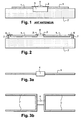
- the detector described in relation to Figures 2 and 3a is equipped with a dipole antenna.
- the antenna can be of the double dipole type (1 '). In doing so, there is a small electrically conductive surface, making it possible to minimize the heat capacity and the radiation losses of the assembly.
- the radiation losses will be low in all cases, because the conductive layers used for the antenna have almost zero emissivities in the infrared (and indeed in almost the entire spectrum from the visible range into the field millimeter) because of the intrinsic characteristics of the materials used.
- the absorption band obtained at -3dB with such a detector is about 1 THz.
- a band centered on 650 GHz or 850 GHz can also be obtained using appropriate filters, such as networks of slots positioned in front of the detector.
- thermometer 10
- dipole antenna or double dipole antenna 11, 11 '
- anchoring points (12) formed on the one hand, in the vicinity of the edges free of the antenna, and secondly, in the immediate vicinity of the thermometer.
- the assembly is again thermally insulated from the substrate (2) by isolation arms (13).
- isolation arms 13
- These are composed either of a single dielectric layer (13) made of silicon oxide SiO or of silicon nitride SiN, or of a dielectric layer surmounted by a resistive layer, for example made of titanium nitride TiN ( 14), to ensure the routing of stimuli at the thermometer.
- the substrate is an SOI substrate, composed of a silicon layer (15) with a thickness between 1 and 20 ⁇ m, of a buried oxide layer (for example SiO) (16) with a thickness of between 3000 Angstroms. and 2 ⁇ m, and a solid substrate (17), which is generally 400 to 500 ⁇ m thick.
- SOI substrate composed of a silicon layer (15) with a thickness between 1 and 20 ⁇ m, of a buried oxide layer (for example SiO) (16) with a thickness of between 3000 Angstroms. and 2 ⁇ m, and a solid substrate (17), which is generally 400 to 500 ⁇ m thick.
- the assembly is integrated in a substrate (18), etched to a thickness equal to ⁇ / 4 where ⁇ is the wavelength of use of the detector, and whose background of the etching is advantageously covered with a conductive layer (19), adapted to act as a reflector.
- This configuration allows the encapsulation of the detector and then imposes a lighting from the rear face.
- the possible doping of these layers is carried out by introducing a doping gas (BF3, PH3, etc.) into the reactor or by ion implantation.
- a doping gas BF3, PH3, etc.
- the etching of these materials is generally performed by plasma etching methods.
- the metallic materials (Ti, TiN, Pt, Al, Pd, Ni, NiCr, etc.) constituting the resistive elements, the electrodes and the various metallizations such as the interconnection lines, the antennas or the antenna load resistance, are also deposited by sputtering, or by thermal decomposition (LPCVD) or plasma (PECVD). These metallizations are defined by chemical etching or plasma etching processes or by a process known in the English term as "lift off”. The thickness of these layers is between 0.005 ⁇ m and 1 ⁇ m.
- the conductive lines and the metal connection pads (20), for example made of aluminum, on which the holding pillars will be manufactured, are produced by deposition, photolithography and etching. These deposits are made on a stack consisting of silicon (15), the buried layer of silicon oxide (116), and the bulk substrate (17).
- One or more metal layers (23, 24), at least one of which is highly conductive (Al, Au) are deposited on the insulating membrane (22), and are intended to form on the one hand the antenna, and on the other hand the polarization electrodes of the thermometer and the load resistance of the antenna (in resistive metal: TiN, TaN ). The whole is engraved through a resin mask (see Figure 6b ).
- one or more metal layers (25) intended to constitute the base of the electrical contacts between the thermometer and the interconnection lines, and for example made of titanium or titanium nitride TiN are deposited and etched ( Figure 6c ).
- a first conductive layer (25) is etched to form the antenna. In the same way, such a conductive layer (25) is etched to form the contact electrodes (see FIG. Figure 6d ).
- the heat-resistive material (6) made of amorphous silicon or vanadium oxide, for example, is deposited and etched through a resin mask that protects the thermometric zone.
- the substrate is then etched by a BOSH plasma-assisted chemical etching (see Figure 6e ).
- the last step is to release structures by etching the sacrificial layer.
- the hood can be etched by wet chemistry. Before depositing it or sticking it under vacuum on the front face (like the embodiment described in connection with the figure 4 , a conductive layer (Al, Au) thick about 1 micron, preceded by a bonding layer (for example titanium) is deposited by sputtering.
- a conductive layer Al, Au
- a bonding layer for example titanium
Landscapes
- Physics & Mathematics (AREA)
- General Physics & Mathematics (AREA)
- Spectroscopy & Molecular Physics (AREA)
- Photometry And Measurement Of Optical Pulse Characteristics (AREA)
- Radiation Pyrometers (AREA)
- Support Of Aerials (AREA)
- Medicines Containing Antibodies Or Antigens For Use As Internal Diagnostic Agents (AREA)
- Details Of Aerials (AREA)
- Aiming, Guidance, Guns With A Light Source, Armor, Camouflage, And Targets (AREA)
- Geophysics And Detection Of Objects (AREA)
- Nuclear Medicine (AREA)
- Measurement Of The Respiration, Hearing Ability, Form, And Blood Characteristics Of Living Organisms (AREA)
Abstract
Description
La présente invention concerne un détecteur bolométrique, ainsi qu'un dispositif de détection d'ondes électromagnétiques notamment situées dans le domaine des ondes millimétriques et submillimétriques mettant en oeuvre un tel détecteur.The present invention relates to a bolometric detector, as well as a device for detecting electromagnetic waves, in particular located in the millimeter and submillimeter wave field using such a detector.
Elle concerne également le procédé de réalisation de ce détecteur.It also relates to the method of producing this detector.
La détection des ondes millimétriques et plus particulièrement submillimétriques présente un certain nombre d'intérêts, notamment sur le plan scientifique et technologique.The detection of millimeter waves and more particularly submillimetric waves presents a certain number of interests, in particular on the scientific and technological level.
En effet, ce domaine de longueurs d'onde correspond à de nombreuses excitations dans la matière (phonons, rotation des molécules, transition intrabandes, ...). Corollairement, la détection de ces ondes et leur interprétation présentent de nombreuses applications, notamment dans le domaine de l'analyse des polluants de l'atmosphère, en biophysique, en raison de l'absorption de ces ondes par les liquides, mais également en télécommunication, en radioastronomie, radars anti-collision, imagerie biomédicale, etc...Indeed, this range of wavelengths corresponds to many excitations in matter (phonons, rotation of molecules, intraband transition, ...). As a corollary, the detection of these waves and their interpretation have many applications, particularly in the field of the analysis of pollutants of the atmosphere, in biophysics, because of the absorption of these waves by the liquids, but also in telecommunications , in radio astronomy, collision avoidance radar, biomedical imaging, etc ...
Deux principes physiques différents sont actuellement mis en oeuvre pour réaliser la détection des ondes millimétriques et submillimétriques.Two different physical principles are currently used to achieve the detection of millimeter and submillimeter waves.
Le premier d'entre eux consiste à détecter les ondes électromagnétiques au moyen d'une antenne de telle sorte à créer un signal électrique, dont le traitement est effectué par un circuit électronique fonctionnant à la fréquence de l'onde. L'inconvénient des détecteurs fonctionnant selon ce premier principe est d'être fortement limité en fréquences.The first of these consists in detecting the electromagnetic waves by means of an antenna so as to create an electrical signal, the processing of which is carried out by an electronic circuit operating at the frequency of the wave. The disadvantage of detectors operating according to this first principle is to be strongly limited in frequencies.
Au surplus, attendu que de tels détecteurs sont généralement agencés selon une structure matricielle, les circuits correspondants génèrent une dissipation de chaleur relativement élevée, de l'ordre de 1 Watt pour une matrice 32x32, constituant un autre inconvénient.In addition, since such detectors are generally arranged in a matrix structure, the corresponding circuits generate a relatively high heat dissipation, of the order of 1 Watt for a 32x32 matrix, constituting another disadvantage.
Le second principe technique connu consiste à mettre en oeuvre une antenne de détection des ondes électromagnétiques, propre à créer un flux calorifique, dont la mesure correspond au signal recherché. Les détecteurs utilisés dans le cadre de ce principe sont traditionnellement constitués par la famille des détecteurs bolométriques.The second known technical principle is to implement an electromagnetic wave detection antenna, capable of creating a heat flow, the measurement of which corresponds to the desired signal. The detectors used in the context of this principle are traditionally constituted by the family of bolometric detectors.
De manière connue, les détecteurs thermiques, famille à laquelle appartiennent les détecteurs bolométriques, absorbent la puissance d'un rayonnement électromagnétique incident, la convertissent en chaleur, qui se transforme ensuite en un signal résultant de l'élévation de température corrélative par rapport à une température de référence, dans une plage déterminée permettant d'associer à ces variations de températures des signaux électriques correspondant à la mesure effective du flux électromagnétique incident. On conçoit cependant, que dès lors que l'on mesure une variation de température, ledit détecteur doit être le plus isolé possible sur le plan thermique, afin que la mesure ne soit pas polluée par les interférences des constituants auxquels il est relié mécaniquement et électriquement.In known manner, the thermal detectors, to which family the bolometric detectors belong, absorb the power of an incident electromagnetic radiation, convert it into heat, which is then transformed into a signal resulting from the correlative temperature rise with respect to a reference temperature in a determined range for associating with these temperature variations electrical signals corresponding to the actual measurement of the incident electromagnetic flux. It is conceivable, however, that when a temperature variation is measured, said detector must be as thermally isolated as possible so that the measurement is not polluted by the interference of the constituents to which it is mechanically and electrically connected. .
Sous l'effet du rayonnement incident, le détecteur s'échauffe et transmet l'élévation de température corrélative au matériau thermique sensible. Cette augmentation de température engendre une variation d'une propriété dudit matériau sensible, telle qu'une apparition de charges électriques par effet pyroélectrique, la variation de la capacité par changement de la constante diélectrique pour les détecteurs capacitifs, la variation de la tension par effet thermoélectrique pour les thermocouples, et la variation de la résistance pour les détecteurs bolométriques.Under the effect of the incident radiation, the detector heats up and transmits the correlative temperature rise to the sensitive thermal material. This increase in temperature causes a variation of a property of said sensitive material, such as an appearance of electric charges by pyroelectric effect, the variation of the capacitance by changing the dielectric constant for the capacitive detectors, the variation of the effect voltage. thermoelectric for thermocouples, and the variation of resistance for bolometric detectors.
Dans le domaine de la détection infrarouge, l'usage de détecteurs bolométriques est largement répandu. Ces détecteurs sont classiquement constitués d'une membrane suspendue, qui comporte une couche mince (typiquement entre 0.1 et 1 micromètre) réalisée en matériau bolométrique sensible à la température, deux électrodes dites coplanaires et un absorbeur, dont la fonction est de capter le rayonnement électromagnétique pour le convertir en chaleur au sein de la structure. La membrane est suspendue au-dessus du substrat - support, par l'intermédiaire de points d'ancrage ou pions de fixation, propres à isoler ladite membrane du substrat. Ces structures, également dénommées piliers permettent d'amener les potentiels d'excitation ou stimuli vers les parties conductrices ou électrodes du détecteur bolométrique via des structures planes et allongées, également appelées bras d'isolement. Elles sont donc conductrices électriquement mais en revanche présentent une résistance thermique la plus élevée possible.In the field of infrared detection, the use of bolometric detectors is widespread. These detectors are conventionally constituted by a suspended membrane, which comprises a thin layer (typically between 0.1 and 1 micrometer) made of a temperature-sensitive bolometric material, two so-called coplanar electrodes and an absorber, whose function is to capture electromagnetic radiation. to convert it into heat within the structure. The membrane is suspended above the support substrate, via anchoring points or fixing pins, adapted to isolate said membrane from the substrate. These structures, also called pillars, can bring the excitation potentials or stimuli to the conductive parts or electrodes of the bolometric detector via flat and elongated structures, also called isolation arms. They are therefore electrically conductive but on the other hand have the highest possible thermal resistance.
Afin d'aboutir à des performances satisfaisantes, le matériau bolométrique, c'est-à-dire le matériau sensible doit présenter une faible masse calorifique, doit être bien isolée thermiquement par rapport au support, et enfin doit présenter une forte sensibilité à l'effet de conversion de l'échauffement en signal électrique.In order to achieve satisfactory performance, the bolometric material, that is to say the sensitive material must have a low heat mass, must be well insulated thermally relative to the support, and finally must have a high sensitivity to the effect of converting the heating into an electrical signal.
De manière connue, le substrat - support, généralement réalisé en silicium, reçoit un circuit de lecture constitué d'un circuit électronique intégrant des moyens d'adressage séquentiel ou de multiplexage des détecteurs élémentaires et des moyens d'excitation électrique (stimuli) et de pré-traitement des signaux électriques générés par lesdits détecteurs élémentaires. Ce faisant, un tel circuit de lecture permet de sérialiser les signaux issus des différents détecteurs élémentaires et de les transmettre vers un nombre réduit de sorties, afin d'être exploités par un système d'imagerie usuel, tel que par exemple une caméra infrarouge.In known manner, the support substrate, generally made of silicon, receives a read circuit constituted by an electronic circuit integrating means of sequential addressing or multiplexing of the elementary detectors and electrical excitation means (stimuli) and of pre-processing the electrical signals generated by said elementary detectors. In doing so, such a read circuit makes it possible to serialize the signals coming from the different elementary detectors and to transmit them to a small number of outputs, in order to be exploited by a usual imaging system, such as for example an infrared camera.
Avantageusement, afin d'optimiser les performances de ces détecteurs, ceux-ci sont encapsulés sous vide ou sous faible pression de gaz inerte conducteur de la chaleur au sein d'un boîtier, muni alors d'une fenêtre transparente à la bande de longueurs d'onde concernée.Advantageously, in order to optimize the performance of these detectors, they are encapsulated under vacuum or under low pressure of inert gas conducting heat within a housing, then provided with a transparent window to the length of the band. concerned wave.
Traditionnellement, le matériau bolométrique mis en oeuvre est constitué de silicium polycristallin ou amorphe de type p ou n faiblement ou fortement résistif, mais peut également être réalisé en oxyde de vanadium (V2O5, VO2) ou d'un cuprate (YBaCuO) élaboré en une phase semi-conductrice.Traditionally, the bolometric material used consists of polycrystalline or amorphous silicon of p-type or n weakly or strongly resistive, but can also be made of vanadium oxide (V 2 O 5 , VO 2 ) or a cuprate (YBaCuO ) developed in a semiconductor phase.
La mise en oeuvre de tels détecteurs bolométriques a été largement décrite en relation avec la détection dans le domaine de l'infrarouge. Pour cette plage de longueur d'ondes, il est possible de réunir simultanément sur la planche bolométrique les fonctions de thermométrie et d'absorption du rayonnement infrarouge incident.The implementation of such bolometric detectors has been widely described in relation to detection in the infrared domain. For this wavelength range, it is possible to simultaneously combine the thermometric and absorption functions of the incident infrared radiation on the bolometric plate.
En effet, un système de détection électromagnétique doit présenter des dimensions voisines de l'ordre de grandeur de la longueur d'onde considérée afin d'être efficace. Il existe un compromis entre la puissance collectée (proportionnelle à la surface du détecteur) et la résolution spatiale. Les phénomènes de diffraction inhérents à tout système optique limitent la résolution spatiale à une valeur de l'ordre de la longueur d'onde dans les dimensions du plan. Les dimensions optimales pour un détecteur sont donc de cet ordre de grandeur.Indeed, an electromagnetic detection system must have dimensions close to the order of magnitude of the wavelength considered in order to be effective. There is a tradeoff between the collected power (proportional to the surface of the detector) and the spatial resolution. The diffraction phenomena inherent in any optical system limit the spatial resolution to a value of the order of the wavelength in the dimensions of the plane. The optimal dimensions for a detector are therefore of this order of magnitude.
Ainsi, une planche ou matrice de détecteurs infrarouges de dimensions de 25 x 25 µm2 est susceptible d'intégrer ces deux fonctions. Ce faisant, l'absorbeur c'est-à-dire la membrane supportant l'élément sensible bolométrique assure à la fois la fonction de couplage électromagnétique avec le rayonnement incident, et donc d'absorption dudit rayonnement, et la fonction de conversion de ce rayonnement en flux calorifique par effet joule.Thus, a board or array of infrared detectors of dimensions 25 x 25 microns 2 is likely to integrate these two functions. In doing so, the absorber, that is to say the membrane supporting the bolometric sensitive element provides both the electromagnetic coupling function with the incident radiation, and therefore the absorption of said radiation, and the conversion function of this radiation. heat flux radiation by Joule effect.
Or, dans le domaine des longueurs d'onde submillimétriques voire millimétriques, le raisonnement précédent conduirait à aboutir à des membranes de même ordre de grandeur. Or, tant la masse calorifique, la tenue mécanique que les pertes par rayonnement d'une membrane de telles dimensions sont inenvisageables pour la pérennité des détecteurs mis en oeuvre outre pour la qualité des mesures à réaliser.However, in the submillimeter wavelength or millimetric wavelength range, the previous reasoning would lead to membranes of the same order of magnitude. However, both the heat mass, the mechanical strength and the radiation losses of a membrane of such dimensions are unthinkable for the durability of the detectors used in addition to the quality of the measurements to be made.
Ce faisant, il devient nécessaire de séparer la fonction de couplage électromagnétique, de la fonction de conversion de la puissance électromagnétique en puissance calorifique. La première de ces deux fonctions est réalisée au moyen d'une antenne réceptrice, et la seconde fonction est assurée par une charge résistive associée à l'antenne.In doing so, it becomes necessary to separate the electromagnetic coupling function from the conversion function of the electromagnetic power into heating power. The first of these two functions is performed by means of a receiving antenna, and the second function is provided by a resistive load associated with the antenna.
On connaît de tels dispositifs de détection bolométrique dits « à antenne », susceptibles de fonctionner à des températures allant de 150 à 300 K, donc à température ambiante. Ces dispositifs mettent en oeuvre des barrettes ou des matrices de tels détecteurs.Such bolometric detection devices known as "antenna" are known, capable of operating at temperatures ranging from 150 to 300 K, therefore at ambient temperature. These devices implement arrays or matrices of such detectors.
On a représenté en relation avec la
Celui-ci est fondamentalement constitué d'une antenne (1) constituée d'une couche conductrice, déposée sur un substrat (2) non conducteur. Elle comprend un métal résistif (3) constituant à la fois la charge résistive de l'antenne, propre à générer la puissance calorifique, et des bras d'isolation d'un thermomètre ou bolomètre (4), composé d'un matériau thermo-résistif, tel que par exemple du silicium amorphe ou oxyde de Vanadium. Comme on peut l'observer, il est défini sous le thermomètre (4) une cavité (5) permettant l'isolation thermique de celui-ci.It basically consists of an antenna (1) consisting of a conductive layer deposited on a non-conductive substrate (2). It comprises a resistive metal (3) constituting both the resistive load of the antenna, suitable for generating the heating power, and the insulating arms of a thermometer or bolometer (4), composed of a thermo-magnetic material. resistive, such as for example amorphous silicon or vanadium oxide. As can be seen, it is defined under the thermometer (4) a cavity (5) for thermal insulation thereof.
Les courants électriques générés dans l'antenne (1) par le rayonnement incident sont dissipés dans les bras d'isolation (3) par effet joule.The electric currents generated in the antenna (1) by the incident radiation are dissipated in the insulation arms (3) by joule effect.
Avantageusement, un plan métallique réflecteur permet d'optimiser l'absorption pour une gamme de longueurs d'onde donnée. Ce réflecteur est en général positionné à une distance égale à n fois λ/4 de l'antenne, n étant un nombre entier.Advantageously, a reflective metal plane optimizes the absorption for a given range of wavelengths. This reflector is generally positioned at a distance equal to n times λ / 4 of the antenna, n being an integer.
On conçoit bien la nécessité d'isoler thermiquement le détecteur proprement dit, en l'espèce réalisé en matériau bolométrique, afin de permettre l'optimisation de la détection. Or, l'une des difficultés à vaincre avec de tels dispositifs de détection réside dans la limitation imposée par construction, liée à la proportionnalité entre la conductance thermique et la conductance électrique dans tout matériau conducteur, et qui prend une forme simple pour les métaux : la loi de Wiedmann Franz.It is well understood the need to thermally isolate the actual detector, in this case made of bolometric material, to allow optimization of the detection. One of the difficulties to overcome with such detection devices lies in the limitation imposed by construction, related to the proportionality between the thermal conductance and the electrical conductance in any conductive material, and which takes a simple form for the metals: the law of Wiedmann Franz.
Ainsi, le lien électrique entre l'antenne et le thermomètre s'accompagne nécessairement d'un lien thermique, ce qui nuit de manière importante aux performances des bolomètres, puisque aussi bien, ceux-ci mesurent une variation de température par rapport à une valeur de référence.Thus, the electrical connection between the antenna and the thermometer is necessarily accompanied by a thermal link, which significantly impairs the performance of the bolometers, since they also measure a variation in temperature with respect to a value. reference.
On a par exemple décrit dans le document
L'antenne de forme particulière est déposée sur une couche d'oxyde de silicium SiO, qui du fait de la technologie employée (de type couche mince) présente une épaisseur e de l'ordre du µm. Une antenne de type « Bow-Tie », optimisée pour détecteur autour d'une fréquence de 1 THz présente une surface S de l'ordre de 300 x 300 µm2, soit environ le carré de la longueur d'onde d'utilisation.The antenna of particular shape is deposited on a layer of silicon oxide SiO, which because of the technology employed (thin film type) has a thickness e of the order of one micron. A " Bow-Tie " type antenna, optimized for a detector around a frequency of 1 THz has a surface S of the order of 300 x 300 μm 2 , about the square of the wavelength of use.
Si l'on néglige les effets de bords, la résistance thermique entre l'antenne et le substrat peut être déterminée par la relation suivante : 
où g représente la conductance thermique du matériau constitutif de l'antenne.If edge effects are neglected, the thermal resistance between the antenna and the substrate can be determined by the following relation:
where g represents the thermal conductance of the constituent material of the antenna.
La conductance thermique du substrat réalisé en oxyde de silicium SiO est de l'ordre de g = 1,35 W.m-1K-1, la résistance thermique entre l'antenne et le substrat est voisine de 10 K/W. L'antenne est donc, dans cette hypothèse, quasiment à la masse thermique ; en d'autres termes, elle n'est pas isolée thermiquement, et en raison de sa connexion mécanique et électrique avec le thermomètre, ce dernier n'est pas isolé thermiquement de façon satisfaisante.The thermal conductance of the substrate made of silicon oxide SiO is of the order of g = 1.35 Wm -1 K -1 , the thermal resistance between the antenna and the substrate is close to 10 K / W. The antenna is, in this case, almost the thermal mass; in other words, it is not thermally insulated, and because of its mechanical and electrical connection with the thermometer, it is not thermally insulated satisfactorily.
Afin de surmonter cet inconvénient, on a proposé dans le document
Là encore, l'antenne n'est pas isolée thermiquement, seul le matériau thermo-résistif constitutif du thermomètre, est effectivement isolé thermiquement du substrat, mais donc pas de l'antenne.Again, the antenna is not thermally insulated, only the constituent thermo-resistive material of the thermometer, is actually thermally isolated from the substrate, but not the antenna.
Enfin, on a suggéré dans le document
En résumé, il n'existe donc pas de solution technique satisfaisante pour permettre d'aboutir de manière relativement simple sur le plan technologique, à une isolation thermique complète ou quasi-complète du thermomètre ou bolomètre.In summary, there is therefore no satisfactory technical solution to achieve a relatively simple way in terms of technology, a complete or almost complete thermal insulation of the thermometer or bolometer.
L'invention propose une solution à ces différents problèmes techniques, bien évidemment dans le domaine de la détection des ondes électromagnétiques millimétriques et submillimétriques.The invention proposes a solution to these various technical problems, obviously in the field of the detection of millimetric and submillimetric electromagnetic waves.
Fondamentalement, le principe général sous-tendant la présente invention repose sur l'isolation thermique de l'antenne par rapport au substrat. Le problème de l'isolation thermique entre le thermomètre et l'antenne ne se pose alors plus, et l'isolation thermique de l'ensemble devenant indépendante de considérations électromagnétiques.Basically, the general principle underlying the present invention is based on the thermal insulation of the antenna with respect to the substrate. The problem of thermal insulation between the thermometer and the antenna does not arise then, and the thermal insulation of the assembly becoming independent of electromagnetic considerations.
Ainsi, l'invention vise tout d'abord un détecteur bolométrique d'un rayonnement électromagnétique, notamment de fréquences comprises entre 100 GHz et 10 THz, selon la revendication 1.Thus, the invention firstly aims at a bolometric detector of electromagnetic radiation, in particular at frequencies between 100 GHz and 10 THz, according to
Selon l'invention, l'antenne réceptrice est elle-même isolée du substrat - support, cette dernière n'étant reliée que très indirectement audit substrat et notamment pas au niveau de ses faces principales.According to the invention, the receiving antenna is itself isolated from the substrate-support, the latter being connected only very indirectly to said substrate and in particular not at its main faces.
En effet, ce faisant on aboutit à une optimisation de l'isolation thermique de l'ensemble constitué par l'antenne, l'élément thermométrique et les charges résistives, puisque aussi bien, le seul contact subsistant n'intervient plus qu'au niveau, notamment des bords libres de l'antenne, c'est-à-dire opposés à l'élément thermométrique.In fact, this leads to an optimization of the thermal insulation of the assembly constituted by the antenna, the thermometric element and the resistive loads, since as well, the only remaining contact intervenes only at the level , in particular free edges of the antenna, that is to say opposite to the thermometric element.
L'ensemble ainsi défini est maintenu suspendu au dessus du substrat avantageusement par le biais de bras d'isolation, conducteurs électriquement mais thermiquement isolants, reposant eux-mêmes sur des points d'ancrage ménagés sur ledit substrat, et solidarisés au niveau des bords libres de l'antenne.The assembly thus defined is held suspended above the substrate advantageously by means of isolation arms, electrically conductive but thermally insulating conductors, themselves resting on anchor points formed on said substrate, and secured at the free edges of the antenna.
Les antennes mis en oeuvre peuvent être du type dipôle, c'est à dire s'étendre de part et d'autre de l'élément thermométrique, ou de type double dipôles, c'est-à-dire muni de deux sorties au niveau de chacune de leurs zones de connexion à l'élément thermométrique.The antennas used may be of the dipole type, that is to say extend on either side of the thermometric element, or of the double dipole type, that is to say provided with two outputs on the each of their connection zones to the thermometric element.
La manière de réaliser l'invention et les avantages qui en découlent ressortiront mieux des exemples de réalisation qui suivent, donnés à titre indicatif et non limitatif à l'appui des figures annexées.
- La
figure 1 est une représentation schématique d'un détecteur bolométrique à antenne conforme à l'état antérieur de la technique. - La
figure 2 est une représentation schématique d'un détecteur bolométrique à antenne selon l'invention. - La
figure 3 illustre en vue de dessus un détecteur conforme à l'invention, respectivement muni sur lafigure 3a d'une antenne dipôle, et sur lafigure 3b d'une antenne double dipôles. - La
figure 4 est une représentation schématique d'un détecteur bolométrique à antenne suspendue sur une cavité quart d'ondes, dont lafigure 5 est une vue du dessus. - Les
figures 6a à 6e illustrent un mode de réalisation dudit détecteur bolométrique conforme à l'invention.
- The
figure 1 is a schematic representation of a bolometric antenna detector according to the prior art. - The
figure 2 is a schematic representation of a bolometric antenna detector according to the invention. - The
figure 3 illustrates in top view a detector according to the invention, respectively provided on thefigure 3a of a dipole antenna, and on thefigure 3b a double dipole antenna. - The
figure 4 is a schematic representation of a bolometric antenna detector suspended on a quarter-wave cavity, whosefigure 5 is a view from above. - The
Figures 6a to 6e illustrate an embodiment of said bolometric detector according to the invention.
Les références numériques désignant les mêmes éléments ont été conservées sur les différentes figures.The numerical references designating the same elements have been preserved in the various figures.
Comme on peut l'observer sur la
Ces bras d'isolation (6) sont isolants thermiquement, de sorte que l'ensemble ainsi défini est lui-même isolé thermiquement du substrat, ce qui constitue l'un des buts essentiels de l'invention.These insulating arms (6) are thermally insulating, so that the assembly thus defined is itself thermally isolated from the substrate, which constitutes one of the essential aims of the invention.
En outre, ces bras (6) sont conducteurs électriquement, de telle sorte à permettre l'acheminement des stimuli au niveau du bolomètre (4), et la collecte des signaux électriques générés par ce dernier, en suite de l'irradiation du détecteur par un rayonnement électromagnétique dans la gamme de longueurs d'onde déterminée.In addition, these arms (6) are electrically conductive, so as to allow the delivery of stimuli at the bolometer (4), and the collection of electrical signals generated by the latter, following irradiation of the detector by electromagnetic radiation in the determined wavelength range.
Le détecteur décrit en relation avec les
Toutefois, les pertes par rayonnement seront dans tous les cas faibles, car les couches conductrices utilisées pour l'antenne ont des émissivités quasiment nulles dans l'infrarouge (et d'ailleurs dans quasiment tout le spectre à partir du domaine visible jusque dans le domaine millimétrique) en raison des caractéristiques intrinsèques des matériaux utilisés.However, the radiation losses will be low in all cases, because the conductive layers used for the antenna have almost zero emissivities in the infrared (and indeed in almost the entire spectrum from the visible range into the field millimeter) because of the intrinsic characteristics of the materials used.
On montre en effet, qu'avec ce type d'antenne double dipôles, par exemple constituée d'un ruban de 1 µm de large, et présentant une longueur totale de 280 µm et une largeur de 140 µm, réalisée en un matériau bon conducteur, tel qu'en métal (Aluminium, Or, etc.), on obtient une résistance thermique voisine de 50 MK/W pour une résistance de charge de 150 Ω, à comparer avec la valeur de 2,5 MK/W que l'on aurait obtenu avec les détecteurs de l'art antérieur. En d'autres termes, l'isolation thermique de l'ensemble suspendu est multipliée d'un facteur 20, contribuant ainsi à aboutir au résultat recherché par la présente invention.It is shown, indeed, that with this type of double dipole antenna, for example consisting of a ribbon of 1 micron wide, and having a total length of 280 microns and a width of 140 microns, made of a good conductor material , such as metal (aluminum, gold, etc.), a thermal resistance close to 50 MK / W is obtained for a load resistance of 150 Ω, compared with the value of 2.5 MK / W that the one would have obtained with the detectors of the prior art. In other words, the thermal insulation of the suspended assembly is multiplied by a factor of 20, thus contributing to achieving the result sought by the present invention.
Au surplus, la bande d'absorption obtenue à -3dB avec un tel détecteur, muni en outre d'un réflecteur métallique (non représenté) positionné à 75 µm sous le bolomètre est d'environ 1 THz.In addition, the absorption band obtained at -3dB with such a detector, further provided with a metal reflector (not shown) positioned at 75 μm under the bolometer is about 1 THz.
Bien évidemment, une bande centrée sur 650 GHz ou 850 GHz peut également être obtenue à l'aide de filtres appropriés, tels que des réseaux de fentes positionnés devant le détecteur.Of course, a band centered on 650 GHz or 850 GHz can also be obtained using appropriate filters, such as networks of slots positioned in front of the detector.
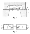
On a représenté en relation avec les
Le substrat est un substrat SOI, composé d'une couche de silicium (15) d'épaisseur comprise entre 1 et 20 µm, d'une couche d'oxyde (par exemple SiO) enterré (16) d'épaisseur comprise entre 3000 Angstrôms et 2 µm, et d'un substrat massif (17), qui possède généralement 400 à 500 µm d'épaisseur.The substrate is an SOI substrate, composed of a silicon layer (15) with a thickness between 1 and 20 μm, of a buried oxide layer (for example SiO) (16) with a thickness of between 3000 Angstroms. and 2 μm, and a solid substrate (17), which is generally 400 to 500 μm thick.
L'ensemble est intégré dans un substrat (18), gravé sur une épaisseur égale à λ/4 où λ est la longueur d'onde d'utilisation du détecteur, et dont le fond de la gravure est avantageusement recouvert d'une couche conductrice (19), propre à faire fonction de réflecteur.The assembly is integrated in a substrate (18), etched to a thickness equal to λ / 4 where λ is the wavelength of use of the detector, and whose background of the etching is advantageously covered with a conductive layer (19), adapted to act as a reflector.
Cette configuration permet l'encapsulation du détecteur et impose alors un éclairage par la face arrière.This configuration allows the encapsulation of the detector and then imposes a lighting from the rear face.
Il va être maintenant décrit plus en détail un mode de réalisation du détecteur bolométrique conforme à l'invention, en relation avec les
Il convient au préalable de rappeler, qu'un certain nombre de techniques classiques en microélectronique sont mises en oeuvre. Ainsi, la réalisation des couches minces de différents éléments (0.005µm à 1µm), en matériau isolant (SiN, SiO, ZnS etc.) et semiconducteur amorphe ou polycristallin (Si, Ge, SiC, a-Si:H, a-SiC:H, a-SiGe:H, etc.), est obtenue à l'aide des techniques de dépôt basse température, habituellement utilisées pour ces matériaux : pulvérisation cathodique, décomposition thermique (LPCVD) ou assistée par plasma (PECVD).It should first be recalled that a number of conventional techniques in microelectronics are implemented. Thus, the production of thin layers of different elements (0.005 μm to 1 μm), of insulating material (SiN, SiO, ZnS etc.) and amorphous or polycrystalline semiconductor (Si, Ge, SiC, a-Si: H, a-SiC : H, a-SiGe: H, etc.), is obtained using the low temperature deposition techniques commonly used for these materials: sputtering, thermal decomposition (LPCVD) or plasma assisted (PECVD).
Le dopage éventuel de ces couches est réalisé en introduisant un gaz dopant (BF3, PH3, etc.) dans le réacteur ou bien par implantation ionique. La gravure de ces matériaux est généralement réalisée par des procédés d'attaque chimique assistée par plasma.The possible doping of these layers is carried out by introducing a doping gas (BF3, PH3, etc.) into the reactor or by ion implantation. The etching of these materials is generally performed by plasma etching methods.
Les matériaux métalliques (Ti, TiN, Pt, Al, Pd, Ni, NiCr, etc.) constituant les éléments résistifs, les électrodes et les diverses métallisations comme les lignes d'interconnexion, les antennes ou la résistance de charge d'antenne, sont également déposées par pulvérisation cathodique, ou par décomposition thermique (LPCVD) ou plasma (PECVD). Ces métallisations sont définies par des procédés de gravure chimique, plasma ou par un procédé limitativement connu sous l'expression anglo-saxonne de "lift off". L'épaisseur de ces couches est comprise entre 0.005 µm et 1 µm.The metallic materials (Ti, TiN, Pt, Al, Pd, Ni, NiCr, etc.) constituting the resistive elements, the electrodes and the various metallizations such as the interconnection lines, the antennas or the antenna load resistance, are also deposited by sputtering, or by thermal decomposition (LPCVD) or plasma (PECVD). These metallizations are defined by chemical etching or plasma etching processes or by a process known in the English term as "lift off". The thickness of these layers is between 0.005 μm and 1 μm.
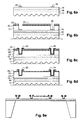
Lors d'une première étape (
Après passivation au moyen d'un dépôt de SiO (non représenté), une couche sacrificielle (21) de 1 à 10 µm d'épaisseur, et par exemple réalisée en polyimide est déposée, puis une membrane isolante électriquement (22), réalisée en SiO ou en SiN par exemple, et dont la fonction est de servir de support mécanique.After passivation by means of an SiO deposition (not shown), a sacrificial layer (21) of 1 to 10 μm in thickness, for example made of polyimide, is deposited, and then an electrically insulating membrane (22) made of SiO or SiN for example, and whose function is to serve as mechanical support.
Une ou plusieurs couches métalliques (23, 24), dont l'une au moins est très conductrice (Al, Au) sont déposées sur la membrane isolante (22), et sont destinées à former d'une part l'antenne, et d'autre part les électrodes de polarisation du thermomètre et la résistance de charge de l'antenne (en métal résistif : TiN, TaN...). Le tout est gravé à travers un masque de résine (voir
Ensuite, une ou plusieurs couches métalliques (25), destinées à constituer la base des contacts électriques entre le thermomètre et les lignes d'interconnexion, et par exemple réalisées en titane ou en nitrure de titane TiN sont déposées puis gravées (
Une première couche conductrice (25) est gravée pour former l'antenne. De la même manière, une telle couche conductrice (25) est gravée afin de constituer les électrodes de contact (voir
Le matériau thermorésistif (6), réalisé en silicium amorphe ou en oxyde de vanadium par exemple, est déposé puis gravé à travers un masque de résine qui protège la zone thermométrique.The heat-resistive material (6), made of amorphous silicon or vanadium oxide, for example, is deposited and etched through a resin mask that protects the thermometric zone.
Le substrat est ensuite gravé par une attaque chimique assistée par plasma de type BOSH (voir
La dernière étape consiste à libérer des structures par gravure de la couche sacrificielle.The last step is to release structures by etching the sacrificial layer.
Le capot, peut être quant à lui gravé par voie chimique humide. Avant de le déposer ou de le coller sous vide en face avant (à l'instar de la réalisation décrite en relation avec la
Claims (8)
- A bolometric detector for electromagnetic radiation comprising:- a receiving antenna (1, 1', 11') intended to collect electromagnetic radiation and thus ensuring electromagnetic coupling;- a resistive load (3) capable of converting the electromagnetic power collected into heating capacity;- a thermometric element (4) connected to the receiving antenna via the resistive load and thermally isolated from a support substrate (2) capable of accommodating an electronic circuit that includes means of electric excitation and means of pre-processing the electric signals generated by said detector ;wherein :- the receiving antenna is itself thermally isolated from the support substrate (2),- the assembly consisting of the receiving antenna (1, 1', 11'), the resistive load (3) and the thermometric element (4) is suspended above the support substrate by means of thermally insulating isolating arms (6, 13, 14) lying on anchoring points (7, 12) made on said support substrate, at least part of said isolating arms (6, 13) being connected on the free edge of the main faces of the receiving antenna.
- A bolometric detector for electromagnetic radiation as claimed in claim 1, wherein the receiving antenna (11') is connected to the isolating arms (14) in the vicinity of the thermometer (4).
- A bolometric detector for electromagnetic radiation as claimed in claim 1 or 2, wherein the isolating arms (6, 14) are electrically conductive.
- A bolometric detector for electromagnetic radiation as claimed in claims 1 to 3, wherein the receiving antenna is of the dipole type or double-dipole type.
- A bolometric detector for electromagnetic radiation as claimed in claims 1 to 4, wherein the thermometric element (4) is made of a bolometric material selected from the group comprising type p or n polycrystalline or amorphous silicon, vanadium oxides (V2O5, VO2) and cuprates (YBaCuO) produced in a semiconductor phase.
- A bolometric detector for electromagnetic radiation according to claims 1 to 5, operating at frequencies from 100 GHz to 10 THz.
- A device for detecting electromagnetic radiation, wherein it consists of a one- or two-dimensional array of elementary bolometric detectors electrically connected to a readout circuit and having the features defined in claims 1 to 6.
- A device for detecting electromagnetic radiation according to claim 7, wherein it operates at frequencies from 100 GHz to 10 THz.
Applications Claiming Priority (1)
| Application Number | Priority Date | Filing Date | Title |
|---|---|---|---|
| FR0503836A FR2884608B1 (en) | 2005-04-18 | 2005-04-18 | BOLOMETRIC DETECTOR, DEVICE FOR DETECTION OF SUBMILLIMETRIC AND MILLIMETRIC ELECTROMAGNETIC WAVES USING SUCH A DETECTOR |
Publications (2)
| Publication Number | Publication Date |
|---|---|
| EP1715315A1 EP1715315A1 (en) | 2006-10-25 |
| EP1715315B1 true EP1715315B1 (en) | 2010-06-23 |
Family
ID=35266742
Family Applications (1)
| Application Number | Title | Priority Date | Filing Date |
|---|---|---|---|
| EP06300295A Not-in-force EP1715315B1 (en) | 2005-04-18 | 2006-03-28 | Bolometric detector, device for the detection of submillimetric and millimetric electromagnetic waves using said detector |
Country Status (6)
| Country | Link |
|---|---|
| US (1) | US7442934B2 (en) |
| EP (1) | EP1715315B1 (en) |
| JP (1) | JP5241077B2 (en) |
| AT (1) | ATE472098T1 (en) |
| DE (1) | DE602006015014D1 (en) |
| FR (1) | FR2884608B1 (en) |
Families Citing this family (22)
| Publication number | Priority date | Publication date | Assignee | Title |
|---|---|---|---|---|
| GB2409337B (en) * | 2002-09-04 | 2005-08-03 | Teraview Ltd | An emitter |
| FI20065776A0 (en) * | 2006-12-05 | 2006-12-05 | Pekka Neittaanmaeki | A method for checking the conductivity of dielectric nanofibers and the corresponding device |
| FR2934044B1 (en) * | 2008-07-17 | 2014-08-15 | Commissariat Energie Atomique | BOLOMETRIC DETECTOR OF ELECTROMAGNETIC WAVES. |
| US8354642B2 (en) * | 2010-10-13 | 2013-01-15 | International Business Machines Corporation | Monolithic passive THz detector with energy concentration on sub-pixel suspended MEMS thermal sensor |
| JP5428783B2 (en) * | 2009-11-12 | 2014-02-26 | 日本電気株式会社 | Bolometer type THz wave detector |
| JP2011237312A (en) * | 2010-05-12 | 2011-11-24 | Hamamatsu Photonics Kk | Terahertz wave detection apparatus and manufacturing method therefor |
| US8570224B2 (en) * | 2010-05-12 | 2013-10-29 | Qualcomm Incorporated | Apparatus providing thermal management for radio frequency devices |
| FR2983952B1 (en) | 2011-12-09 | 2013-11-15 | Commissariat Energie Atomique | BOLOMETRIC DETECTOR FOR ELECTROMAGNETIC RADIATION IN THE FIELD OF TERAHERTZ |
| FR2983953B1 (en) | 2011-12-09 | 2014-01-03 | Commissariat Energie Atomique | BOLOMETRIC DETECTOR OF ELECTROMAGNETIC RADIATION IN THE DOMAIN OF TERAHERTZ AND MATRIX DETECTION DEVICE COMPRISING SUCH DETECTORS |
| RU2511275C2 (en) * | 2012-07-16 | 2014-04-10 | Федеральное государственное унитарное предприятие "Научно-исследовательский институт физических проблем им. Ф.В. Лукина" | Nanostructural ir-receiver (bolometer) with big absorption surface |
| GB2507306A (en) * | 2012-10-25 | 2014-04-30 | Ibm | An antenna-coupled bolometer device for sensing electromagnetic radiation |
| US9052234B2 (en) | 2012-10-30 | 2015-06-09 | International Business Machines Corporation | Dipole antenna with reflectors having low thermal mass for detection of Terahertz radiation |
| US20140117237A1 (en) | 2012-10-30 | 2014-05-01 | International Business Machines Corporation | High responsivity device for thermal sensing in a terahertz radiation detector |
| US8957379B2 (en) | 2012-10-30 | 2015-02-17 | International Business Machines Corporation | Suspended wideband planar skirt antenna having low thermal mass for detection of terahertz radiation |
| US9759693B2 (en) | 2012-12-20 | 2017-09-12 | International Business Machines Corporation | Method of simulating the absorption of plane waves using FEM software tools |
| GB2513170B (en) * | 2013-04-18 | 2020-07-08 | Univ Of Ljubljana | Bolometric detection system with reflecting cavity |
| FR3009865B1 (en) * | 2013-08-22 | 2015-07-31 | Commissariat Energie Atomique | BOLOMETRIC DETECTOR WITH REINFORCED THERMALIZATION COMPENSATION BOLOMETER |
| US20150241281A1 (en) * | 2014-02-27 | 2015-08-27 | International Business Machines Corporation | Bolometer device for sensing electromagnetic radiation |
| JP6486695B2 (en) * | 2015-01-14 | 2019-03-20 | 浜松ホトニクス株式会社 | Bolometer type THz detector |
| CN105371966B (en) * | 2015-11-13 | 2019-01-11 | 南方科技大学 | Novel bolometer and manufacturing method |
| CN111224232B (en) * | 2018-11-23 | 2022-10-18 | 比亚迪股份有限公司 | Dual-band omnidirectional antenna and train |
| US12320707B2 (en) * | 2021-05-11 | 2025-06-03 | The United States Of America As Represented By The Secretary Of The Army | Phonon disruptors for increased thermal resistance without sacrificing electrical signal quality in thermal sensors using alloy and intermetallic materials |
Family Cites Families (9)
| Publication number | Priority date | Publication date | Assignee | Title |
|---|---|---|---|---|
| JPH0627170A (en) * | 1992-07-08 | 1994-02-04 | Sanyo Electric Co Ltd | Superconducting electromagnetic wave detection element |
| IL124691A (en) * | 1995-12-04 | 2001-06-14 | Lockheed Martin Ir Imaging Sys | Infrared radiation detector having a reduced active area |
| FI107407B (en) * | 1997-09-16 | 2001-07-31 | Metorex Internat Oy | An imaging system functioning at the submillimeter wavelength |
| US6329655B1 (en) * | 1998-10-07 | 2001-12-11 | Raytheon Company | Architecture and method of coupling electromagnetic energy to thermal detectors |
| FR2788129B1 (en) | 1998-12-30 | 2001-02-16 | Commissariat Energie Atomique | BOLOMETRIC DETECTOR WITH ANTENNA |
| US6292140B1 (en) * | 1999-11-03 | 2001-09-18 | Hypres, Inc. | Antenna for millimeter-wave imaging and bolometer employing the antenna |
| FR2845157B1 (en) * | 2002-10-01 | 2004-11-05 | Commissariat Energie Atomique | BOLOMETRIC DETECTOR WITH ANTENNA HAVING A SWITCH AND IMAGING DEVICE COMPRISING SAME. |
| FR2855609B1 (en) * | 2003-05-26 | 2005-07-01 | Commissariat Energie Atomique | OPTIMIZED CAVITY BULOMETRIC ANTENNA DETECTION DEVICE FOR MILLIMETRIC OR SUBMILLIMETRIC ELECTROMAGNETIC WAVES, AND METHOD OF MANUFACTURING THE SAME |
| WO2006039571A2 (en) * | 2004-10-01 | 2006-04-13 | Northrop Grumman Corporation | Focal plane antenna to sensor interface for an ultra-sensitive bolometer based sensor |
-
2005
- 2005-04-18 FR FR0503836A patent/FR2884608B1/en not_active Expired - Fee Related
-
2006
- 2006-03-28 EP EP06300295A patent/EP1715315B1/en not_active Not-in-force
- 2006-03-28 DE DE602006015014T patent/DE602006015014D1/en active Active
- 2006-03-28 AT AT06300295T patent/ATE472098T1/en not_active IP Right Cessation
- 2006-03-30 JP JP2006095481A patent/JP5241077B2/en not_active Expired - Fee Related
- 2006-03-30 US US11/393,973 patent/US7442934B2/en not_active Expired - Fee Related
Also Published As
| Publication number | Publication date |
|---|---|
| JP2006304290A (en) | 2006-11-02 |
| ATE472098T1 (en) | 2010-07-15 |
| FR2884608B1 (en) | 2007-05-25 |
| FR2884608A1 (en) | 2006-10-20 |
| US20060231761A1 (en) | 2006-10-19 |
| JP5241077B2 (en) | 2013-07-17 |
| EP1715315A1 (en) | 2006-10-25 |
| US7442934B2 (en) | 2008-10-28 |
| DE602006015014D1 (en) | 2010-08-05 |
Similar Documents
| Publication | Publication Date | Title |
|---|---|---|
| EP1715315B1 (en) | Bolometric detector, device for the detection of submillimetric and millimetric electromagnetic waves using said detector | |
| EP2246677B1 (en) | Bolometric detector of electromagnetic radiation from the infrared to the terahertz spectral domain and detector array device comprising said detectors. | |
| EP2602598B1 (en) | Bolometric detector for electromagnetic radiation in the terahertz spectral band and detector matrix comprising such detectors | |
| EP2340422A1 (en) | Bolometric detector for detecting electromagnetic waves | |
| EP0971219B1 (en) | Thermal detector with amplification by bolometric effect | |
| EP1880176B1 (en) | Thermal detector for electromagnetic radiation and infrared detection device using said detectors | |
| EP0828145B1 (en) | Infrared detector and process for manufacturing it | |
| EP2700922B1 (en) | Bolometric detector of electromagnetic radiation in the terahertz range and matrix detection device comprising such detectors | |
| WO2004025694A2 (en) | .electromagnetic radiation sensing device with integrated housing including two superimposed sensors | |
| FR2735574A1 (en) | BOLOMETRIC DETECTION DEVICE FOR MILLIMETRIC AND SUBMILLIMETRIC WAVES AND METHOD OF MANUFACTURING THE SAME | |
| EP1482289B1 (en) | Bolometric detection method of (sub-)millimeter waves using an antenna coupled bolometer having a cavity | |
| EP2602599A1 (en) | Bolometric detector for detecting Teraherz electromagnetic radiation | |
| CA2959650A1 (en) | Heat pattern sensors with encapsulated bolometers | |
| EP2715296A1 (en) | Spectroscopic detector and corresponding method | |
| EP2902758A1 (en) | Photon radiation detector comprising an array of antennas and a spiral resistive support | |
| WO2019229353A1 (en) | Sensitive pixel based detection system comprising a thermal detector and a compensation device | |
| FR3066017B1 (en) | PYROELECTRIC INFRARED DETECTION DEVICE HAVING INFRARED MODULATION TRANSMITTER | |
| FR2885690A1 (en) | THERMAL DETECTOR FOR ELECTROMAGNETIC RADIATION AND INFRARED DETECTION DEVICE COMPRISING SUCH DETECTORS | |
| WO2019043312A1 (en) | Electromagnetic radiation detector | |
| EP1750107B1 (en) | Thermal electromagnetic radiation detector using directed insulating components and detection device implementing said detectors | |
| FR3125585A1 (en) | INFRARED IMAGING MICRO-BOLOMETER | |
| FR3004001A1 (en) | ELECTROMAGNETIC WAVE DETECTOR WITH IMPROVED WAVE LENGTH SELECTION PROPERTIES |
Legal Events
| Date | Code | Title | Description |
|---|---|---|---|
| PUAI | Public reference made under article 153(3) epc to a published international application that has entered the european phase |
Free format text: ORIGINAL CODE: 0009012 |
|
| 17P | Request for examination filed |
Effective date: 20060823 |
|
| AK | Designated contracting states |
Kind code of ref document: A1 Designated state(s): AT BE BG CH CY CZ DE DK EE ES FI FR GB GR HU IE IS IT LI LT LU LV MC NL PL PT RO SE SI SK TR |
|
| AX | Request for extension of the european patent |
Extension state: AL BA HR MK YU |
|
| AKX | Designation fees paid |
Designated state(s): AT BE BG CH CY CZ DE DK EE ES FI FR GB GR HU IE IS IT LI LT LU LV MC NL PL PT RO SE SI SK TR |
|
| 17Q | First examination report despatched |
Effective date: 20070713 |
|
| APBK | Appeal reference recorded |
Free format text: ORIGINAL CODE: EPIDOSNREFNE |
|
| APBN | Date of receipt of notice of appeal recorded |
Free format text: ORIGINAL CODE: EPIDOSNNOA2E |
|
| APBR | Date of receipt of statement of grounds of appeal recorded |
Free format text: ORIGINAL CODE: EPIDOSNNOA3E |
|
| APAF | Appeal reference modified |
Free format text: ORIGINAL CODE: EPIDOSCREFNE |
|
| APBT | Appeal procedure closed |
Free format text: ORIGINAL CODE: EPIDOSNNOA9E |
|
| GRAP | Despatch of communication of intention to grant a patent |
Free format text: ORIGINAL CODE: EPIDOSNIGR1 |
|
| GRAS | Grant fee paid |
Free format text: ORIGINAL CODE: EPIDOSNIGR3 |
|
| RAP1 | Party data changed (applicant data changed or rights of an application transferred) |
Owner name: COMMISSARIAT A L'ENERGIE ATOMIQUE ET AUX ENERGIES |
|
| GRAA | (expected) grant |
Free format text: ORIGINAL CODE: 0009210 |
|
| AK | Designated contracting states |
Kind code of ref document: B1 Designated state(s): AT BE BG CH CY CZ DE DK EE ES FI FR GB GR HU IE IS IT LI LT LU LV MC NL PL PT RO SE SI SK TR |
|
| REG | Reference to a national code |
Ref country code: CH Ref legal event code: EP |
|
| REG | Reference to a national code |
Ref country code: IE Ref legal event code: FG4D Free format text: LANGUAGE OF EP DOCUMENT: FRENCH |
|
| REF | Corresponds to: |
Ref document number: 602006015014 Country of ref document: DE Date of ref document: 20100805 Kind code of ref document: P |
|
| REG | Reference to a national code |
Ref country code: NL Ref legal event code: VDEP Effective date: 20100623 |
|
| PG25 | Lapsed in a contracting state [announced via postgrant information from national office to epo] |
Ref country code: SE Free format text: LAPSE BECAUSE OF FAILURE TO SUBMIT A TRANSLATION OF THE DESCRIPTION OR TO PAY THE FEE WITHIN THE PRESCRIBED TIME-LIMIT Effective date: 20100623 Ref country code: LT Free format text: LAPSE BECAUSE OF FAILURE TO SUBMIT A TRANSLATION OF THE DESCRIPTION OR TO PAY THE FEE WITHIN THE PRESCRIBED TIME-LIMIT Effective date: 20100623 |
|
| LTIE | Lt: invalidation of european patent or patent extension |
Effective date: 20100623 |
|
| PG25 | Lapsed in a contracting state [announced via postgrant information from national office to epo] |
Ref country code: SI Free format text: LAPSE BECAUSE OF FAILURE TO SUBMIT A TRANSLATION OF THE DESCRIPTION OR TO PAY THE FEE WITHIN THE PRESCRIBED TIME-LIMIT Effective date: 20100623 Ref country code: LV Free format text: LAPSE BECAUSE OF FAILURE TO SUBMIT A TRANSLATION OF THE DESCRIPTION OR TO PAY THE FEE WITHIN THE PRESCRIBED TIME-LIMIT Effective date: 20100623 Ref country code: FI Free format text: LAPSE BECAUSE OF FAILURE TO SUBMIT A TRANSLATION OF THE DESCRIPTION OR TO PAY THE FEE WITHIN THE PRESCRIBED TIME-LIMIT Effective date: 20100623 Ref country code: AT Free format text: LAPSE BECAUSE OF FAILURE TO SUBMIT A TRANSLATION OF THE DESCRIPTION OR TO PAY THE FEE WITHIN THE PRESCRIBED TIME-LIMIT Effective date: 20100623 |
|
| PG25 | Lapsed in a contracting state [announced via postgrant information from national office to epo] |
Ref country code: GR Free format text: LAPSE BECAUSE OF FAILURE TO SUBMIT A TRANSLATION OF THE DESCRIPTION OR TO PAY THE FEE WITHIN THE PRESCRIBED TIME-LIMIT Effective date: 20100924 Ref country code: PL Free format text: LAPSE BECAUSE OF FAILURE TO SUBMIT A TRANSLATION OF THE DESCRIPTION OR TO PAY THE FEE WITHIN THE PRESCRIBED TIME-LIMIT Effective date: 20100623 |
|
| PG25 | Lapsed in a contracting state [announced via postgrant information from national office to epo] |
Ref country code: EE Free format text: LAPSE BECAUSE OF FAILURE TO SUBMIT A TRANSLATION OF THE DESCRIPTION OR TO PAY THE FEE WITHIN THE PRESCRIBED TIME-LIMIT Effective date: 20100623 Ref country code: NL Free format text: LAPSE BECAUSE OF FAILURE TO SUBMIT A TRANSLATION OF THE DESCRIPTION OR TO PAY THE FEE WITHIN THE PRESCRIBED TIME-LIMIT Effective date: 20100623 |
|
| REG | Reference to a national code |
Ref country code: IE Ref legal event code: FD4D |
|
| PG25 | Lapsed in a contracting state [announced via postgrant information from national office to epo] |
Ref country code: SK Free format text: LAPSE BECAUSE OF FAILURE TO SUBMIT A TRANSLATION OF THE DESCRIPTION OR TO PAY THE FEE WITHIN THE PRESCRIBED TIME-LIMIT Effective date: 20100623 Ref country code: RO Free format text: LAPSE BECAUSE OF FAILURE TO SUBMIT A TRANSLATION OF THE DESCRIPTION OR TO PAY THE FEE WITHIN THE PRESCRIBED TIME-LIMIT Effective date: 20100623 Ref country code: PT Free format text: LAPSE BECAUSE OF FAILURE TO SUBMIT A TRANSLATION OF THE DESCRIPTION OR TO PAY THE FEE WITHIN THE PRESCRIBED TIME-LIMIT Effective date: 20101025 Ref country code: IS Free format text: LAPSE BECAUSE OF FAILURE TO SUBMIT A TRANSLATION OF THE DESCRIPTION OR TO PAY THE FEE WITHIN THE PRESCRIBED TIME-LIMIT Effective date: 20101023 Ref country code: CZ Free format text: LAPSE BECAUSE OF FAILURE TO SUBMIT A TRANSLATION OF THE DESCRIPTION OR TO PAY THE FEE WITHIN THE PRESCRIBED TIME-LIMIT Effective date: 20100623 Ref country code: CY Free format text: LAPSE BECAUSE OF FAILURE TO SUBMIT A TRANSLATION OF THE DESCRIPTION OR TO PAY THE FEE WITHIN THE PRESCRIBED TIME-LIMIT Effective date: 20100623 |
|
| PG25 | Lapsed in a contracting state [announced via postgrant information from national office to epo] |
Ref country code: DK Free format text: LAPSE BECAUSE OF FAILURE TO SUBMIT A TRANSLATION OF THE DESCRIPTION OR TO PAY THE FEE WITHIN THE PRESCRIBED TIME-LIMIT Effective date: 20100623 Ref country code: IE Free format text: LAPSE BECAUSE OF FAILURE TO SUBMIT A TRANSLATION OF THE DESCRIPTION OR TO PAY THE FEE WITHIN THE PRESCRIBED TIME-LIMIT Effective date: 20100623 |
|
| PLBE | No opposition filed within time limit |
Free format text: ORIGINAL CODE: 0009261 |
|
| STAA | Information on the status of an ep patent application or granted ep patent |
Free format text: STATUS: NO OPPOSITION FILED WITHIN TIME LIMIT |
|
| 26N | No opposition filed |
Effective date: 20110324 |
|
| REG | Reference to a national code |
Ref country code: DE Ref legal event code: R097 Ref document number: 602006015014 Country of ref document: DE Effective date: 20110323 |
|
| BERE | Be: lapsed |
Owner name: COMMISSARIAT A L'ENERGIE ATOMIQUE ET AUX ENERGIES Effective date: 20110331 |
|
| PG25 | Lapsed in a contracting state [announced via postgrant information from national office to epo] |
Ref country code: MC Free format text: LAPSE BECAUSE OF NON-PAYMENT OF DUE FEES Effective date: 20110331 |
|
| REG | Reference to a national code |
Ref country code: CH Ref legal event code: PL |
|
| REG | Reference to a national code |
Ref country code: FR Ref legal event code: ST Effective date: 20111130 |
|
| PG25 | Lapsed in a contracting state [announced via postgrant information from national office to epo] |
Ref country code: BE Free format text: LAPSE BECAUSE OF NON-PAYMENT OF DUE FEES Effective date: 20110331 |
|
| PG25 | Lapsed in a contracting state [announced via postgrant information from national office to epo] |
Ref country code: CH Free format text: LAPSE BECAUSE OF NON-PAYMENT OF DUE FEES Effective date: 20110331 Ref country code: LI Free format text: LAPSE BECAUSE OF NON-PAYMENT OF DUE FEES Effective date: 20110331 Ref country code: FR Free format text: LAPSE BECAUSE OF NON-PAYMENT OF DUE FEES Effective date: 20110331 |
|
| PG25 | Lapsed in a contracting state [announced via postgrant information from national office to epo] |
Ref country code: LU Free format text: LAPSE BECAUSE OF NON-PAYMENT OF DUE FEES Effective date: 20110328 |
|
| PG25 | Lapsed in a contracting state [announced via postgrant information from national office to epo] |
Ref country code: BG Free format text: LAPSE BECAUSE OF FAILURE TO SUBMIT A TRANSLATION OF THE DESCRIPTION OR TO PAY THE FEE WITHIN THE PRESCRIBED TIME-LIMIT Effective date: 20100923 Ref country code: TR Free format text: LAPSE BECAUSE OF FAILURE TO SUBMIT A TRANSLATION OF THE DESCRIPTION OR TO PAY THE FEE WITHIN THE PRESCRIBED TIME-LIMIT Effective date: 20100623 |
|
| PG25 | Lapsed in a contracting state [announced via postgrant information from national office to epo] |
Ref country code: ES Free format text: LAPSE BECAUSE OF FAILURE TO SUBMIT A TRANSLATION OF THE DESCRIPTION OR TO PAY THE FEE WITHIN THE PRESCRIBED TIME-LIMIT Effective date: 20101004 Ref country code: HU Free format text: LAPSE BECAUSE OF FAILURE TO SUBMIT A TRANSLATION OF THE DESCRIPTION OR TO PAY THE FEE WITHIN THE PRESCRIBED TIME-LIMIT Effective date: 20100623 |
|
| PGFP | Annual fee paid to national office [announced via postgrant information from national office to epo] |
Ref country code: GB Payment date: 20190320 Year of fee payment: 14 Ref country code: IT Payment date: 20190312 Year of fee payment: 14 Ref country code: DE Payment date: 20190312 Year of fee payment: 14 |
|
| REG | Reference to a national code |
Ref country code: DE Ref legal event code: R119 Ref document number: 602006015014 Country of ref document: DE |
|
| PG25 | Lapsed in a contracting state [announced via postgrant information from national office to epo] |
Ref country code: DE Free format text: LAPSE BECAUSE OF NON-PAYMENT OF DUE FEES Effective date: 20201001 |
|
| GBPC | Gb: european patent ceased through non-payment of renewal fee |
Effective date: 20200328 |
|
| PG25 | Lapsed in a contracting state [announced via postgrant information from national office to epo] |
Ref country code: GB Free format text: LAPSE BECAUSE OF NON-PAYMENT OF DUE FEES Effective date: 20200328 |
|
| PG25 | Lapsed in a contracting state [announced via postgrant information from national office to epo] |
Ref country code: IT Free format text: LAPSE BECAUSE OF NON-PAYMENT OF DUE FEES Effective date: 20200328 |