JP5241077B2 - Bolometer detector and apparatus for detecting submillimeter and millimeter wave electromagnetic waves using the same - Google Patents
Bolometer detector and apparatus for detecting submillimeter and millimeter wave electromagnetic waves using the same Download PDFInfo
- Publication number
- JP5241077B2 JP5241077B2 JP2006095481A JP2006095481A JP5241077B2 JP 5241077 B2 JP5241077 B2 JP 5241077B2 JP 2006095481 A JP2006095481 A JP 2006095481A JP 2006095481 A JP2006095481 A JP 2006095481A JP 5241077 B2 JP5241077 B2 JP 5241077B2
- Authority
- JP
- Japan
- Prior art keywords
- detector
- bolometer
- antenna
- receiving antenna
- support substrate
- Prior art date
- Legal status (The legal status is an assumption and is not a legal conclusion. Google has not performed a legal analysis and makes no representation as to the accuracy of the status listed.)
- Expired - Fee Related
Links
- 239000000758 substrate Substances 0.000 claims abstract description 35
- 230000005670 electromagnetic radiation Effects 0.000 claims abstract description 11
- 230000005284 excitation Effects 0.000 claims abstract description 5
- 238000007781 pre-processing Methods 0.000 claims abstract description 5
- 239000000463 material Substances 0.000 claims description 15
- 230000005855 radiation Effects 0.000 claims description 11
- 229910021417 amorphous silicon Inorganic materials 0.000 claims description 6
- 238000004873 anchoring Methods 0.000 claims description 5
- 238000000926 separation method Methods 0.000 claims description 5
- XHCLAFWTIXFWPH-UHFFFAOYSA-N [O-2].[O-2].[O-2].[O-2].[O-2].[V+5].[V+5] Chemical compound [O-2].[O-2].[O-2].[O-2].[O-2].[V+5].[V+5] XHCLAFWTIXFWPH-UHFFFAOYSA-N 0.000 claims description 4
- 229910001935 vanadium oxide Inorganic materials 0.000 claims description 4
- 229910021420 polycrystalline silicon Inorganic materials 0.000 claims description 3
- 229920005591 polysilicon Polymers 0.000 claims description 3
- 239000004065 semiconductor Substances 0.000 claims description 3
- QPLDLSVMHZLSFG-UHFFFAOYSA-N Copper oxide Chemical compound [Cu]=O QPLDLSVMHZLSFG-UHFFFAOYSA-N 0.000 claims description 2
- 239000005751 Copper oxide Substances 0.000 claims description 2
- 229910000431 copper oxide Inorganic materials 0.000 claims description 2
- 230000008878 coupling Effects 0.000 abstract description 8
- 238000010168 coupling process Methods 0.000 abstract description 8
- 238000005859 coupling reaction Methods 0.000 abstract description 8
- 229910052751 metal Inorganic materials 0.000 description 10
- 239000002184 metal Substances 0.000 description 10
- 238000000034 method Methods 0.000 description 8
- 238000010586 diagram Methods 0.000 description 7
- 230000000694 effects Effects 0.000 description 7
- LIVNPJMFVYWSIS-UHFFFAOYSA-N silicon monoxide Chemical compound [Si-]#[O+] LIVNPJMFVYWSIS-UHFFFAOYSA-N 0.000 description 7
- 238000001514 detection method Methods 0.000 description 6
- 238000010521 absorption reaction Methods 0.000 description 5
- 239000010408 film Substances 0.000 description 5
- 239000012528 membrane Substances 0.000 description 5
- 229910052710 silicon Inorganic materials 0.000 description 5
- VYPSYNLAJGMNEJ-UHFFFAOYSA-N Silicium dioxide Chemical compound O=[Si]=O VYPSYNLAJGMNEJ-UHFFFAOYSA-N 0.000 description 4
- XUIMIQQOPSSXEZ-UHFFFAOYSA-N Silicon Chemical compound [Si] XUIMIQQOPSSXEZ-UHFFFAOYSA-N 0.000 description 4
- ATJFFYVFTNAWJD-UHFFFAOYSA-N Tin Chemical compound [Sn] ATJFFYVFTNAWJD-UHFFFAOYSA-N 0.000 description 4
- 229910052782 aluminium Inorganic materials 0.000 description 4
- 238000005530 etching Methods 0.000 description 4
- 230000004907 flux Effects 0.000 description 4
- 238000009413 insulation Methods 0.000 description 4
- 238000002955 isolation Methods 0.000 description 4
- 238000005259 measurement Methods 0.000 description 4
- 239000010703 silicon Substances 0.000 description 4
- 229910052814 silicon oxide Inorganic materials 0.000 description 4
- 229910052718 tin Inorganic materials 0.000 description 4
- 238000003486 chemical etching Methods 0.000 description 3
- 238000000151 deposition Methods 0.000 description 3
- 238000004518 low pressure chemical vapour deposition Methods 0.000 description 3
- 238000000623 plasma-assisted chemical vapour deposition Methods 0.000 description 3
- 230000008569 process Effects 0.000 description 3
- 238000004544 sputter deposition Methods 0.000 description 3
- NRTOMJZYCJJWKI-UHFFFAOYSA-N Titanium nitride Chemical compound [Ti]#N NRTOMJZYCJJWKI-UHFFFAOYSA-N 0.000 description 2
- 239000006096 absorbing agent Substances 0.000 description 2
- XAGFODPZIPBFFR-UHFFFAOYSA-N aluminium Chemical compound [Al] XAGFODPZIPBFFR-UHFFFAOYSA-N 0.000 description 2
- 238000006243 chemical reaction Methods 0.000 description 2
- 239000004020 conductor Substances 0.000 description 2
- 238000007667 floating Methods 0.000 description 2
- 229910052737 gold Inorganic materials 0.000 description 2
- 239000010931 gold Substances 0.000 description 2
- 238000010438 heat treatment Methods 0.000 description 2
- 239000011159 matrix material Substances 0.000 description 2
- 150000002739 metals Chemical class 0.000 description 2
- 239000011347 resin Substances 0.000 description 2
- 229920005989 resin Polymers 0.000 description 2
- 239000007787 solid Substances 0.000 description 2
- 230000000638 stimulation Effects 0.000 description 2
- 239000010936 titanium Substances 0.000 description 2
- 239000004642 Polyimide Substances 0.000 description 1
- 229910052581 Si3N4 Inorganic materials 0.000 description 1
- 229910000577 Silicon-germanium Inorganic materials 0.000 description 1
- RTAQQCXQSZGOHL-UHFFFAOYSA-N Titanium Chemical compound [Ti] RTAQQCXQSZGOHL-UHFFFAOYSA-N 0.000 description 1
- 230000002411 adverse Effects 0.000 description 1
- 238000003491 array Methods 0.000 description 1
- 238000009529 body temperature measurement Methods 0.000 description 1
- VNNRSPGTAMTISX-UHFFFAOYSA-N chromium nickel Chemical compound [Cr].[Ni] VNNRSPGTAMTISX-UHFFFAOYSA-N 0.000 description 1
- 230000001934 delay Effects 0.000 description 1
- 230000008021 deposition Effects 0.000 description 1
- 238000002059 diagnostic imaging Methods 0.000 description 1
- GNTDGMZSJNCJKK-UHFFFAOYSA-N divanadium pentaoxide Chemical compound O=[V](=O)O[V](=O)=O GNTDGMZSJNCJKK-UHFFFAOYSA-N 0.000 description 1
- 239000002019 doping agent Substances 0.000 description 1
- 230000005611 electricity Effects 0.000 description 1
- 238000005516 engineering process Methods 0.000 description 1
- 239000003344 environmental pollutant Substances 0.000 description 1
- 239000007789 gas Substances 0.000 description 1
- 229910052732 germanium Inorganic materials 0.000 description 1
- PCHJSUWPFVWCPO-UHFFFAOYSA-N gold Chemical compound [Au] PCHJSUWPFVWCPO-UHFFFAOYSA-N 0.000 description 1
- 230000017525 heat dissipation Effects 0.000 description 1
- 238000005286 illumination Methods 0.000 description 1
- 238000003384 imaging method Methods 0.000 description 1
- 239000011261 inert gas Substances 0.000 description 1
- 239000011810 insulating material Substances 0.000 description 1
- 238000005468 ion implantation Methods 0.000 description 1
- 239000007788 liquid Substances 0.000 description 1
- 238000004519 manufacturing process Methods 0.000 description 1
- 239000007769 metal material Substances 0.000 description 1
- 238000004377 microelectronic Methods 0.000 description 1
- 229910003465 moissanite Inorganic materials 0.000 description 1
- 229910021421 monocrystalline silicon Inorganic materials 0.000 description 1
- 229910001120 nichrome Inorganic materials 0.000 description 1
- 229910052759 nickel Inorganic materials 0.000 description 1
- 230000003287 optical effect Effects 0.000 description 1
- 238000005457 optimization Methods 0.000 description 1
- 229910052763 palladium Inorganic materials 0.000 description 1
- 238000002161 passivation Methods 0.000 description 1
- 238000000206 photolithography Methods 0.000 description 1
- 238000001020 plasma etching Methods 0.000 description 1
- 229910052697 platinum Inorganic materials 0.000 description 1
- 231100000719 pollutant Toxicity 0.000 description 1
- 229920001721 polyimide Polymers 0.000 description 1
- 230000002265 prevention Effects 0.000 description 1
- 230000005616 pyroelectricity Effects 0.000 description 1
- 229910010271 silicon carbide Inorganic materials 0.000 description 1
- HQVNEWCFYHHQES-UHFFFAOYSA-N silicon nitride Chemical compound N12[Si]34N5[Si]62N3[Si]51N64 HQVNEWCFYHHQES-UHFFFAOYSA-N 0.000 description 1
- 230000003595 spectral effect Effects 0.000 description 1
- 239000000126 substance Substances 0.000 description 1
- 239000010409 thin film Substances 0.000 description 1
- 229910052719 titanium Inorganic materials 0.000 description 1
- 230000007704 transition Effects 0.000 description 1
- 238000007704 wet chemistry method Methods 0.000 description 1
Images


Classifications
-
- G—PHYSICS
- G01—MEASURING; TESTING
- G01J—MEASUREMENT OF INTENSITY, VELOCITY, SPECTRAL CONTENT, POLARISATION, PHASE OR PULSE CHARACTERISTICS OF INFRARED, VISIBLE OR ULTRAVIOLET LIGHT; COLORIMETRY; RADIATION PYROMETRY
- G01J5/00—Radiation pyrometry, e.g. infrared or optical thermometry
- G01J5/10—Radiation pyrometry, e.g. infrared or optical thermometry using electric radiation detectors
- G01J5/20—Radiation pyrometry, e.g. infrared or optical thermometry using electric radiation detectors using resistors, thermistors or semiconductors sensitive to radiation, e.g. photoconductive devices
-
- G—PHYSICS
- G01—MEASURING; TESTING
- G01J—MEASUREMENT OF INTENSITY, VELOCITY, SPECTRAL CONTENT, POLARISATION, PHASE OR PULSE CHARACTERISTICS OF INFRARED, VISIBLE OR ULTRAVIOLET LIGHT; COLORIMETRY; RADIATION PYROMETRY
- G01J5/00—Radiation pyrometry, e.g. infrared or optical thermometry
- G01J5/02—Constructional details
- G01J5/08—Optical arrangements
- G01J5/0837—Microantennas, e.g. bow-tie
-
- H—ELECTRICITY
- H01—ELECTRIC ELEMENTS
- H01Q—ANTENNAS, i.e. RADIO AERIALS
- H01Q1/00—Details of, or arrangements associated with, antennas
- H01Q1/36—Structural form of radiating elements, e.g. cone, spiral, umbrella; Particular materials used therewith
- H01Q1/38—Structural form of radiating elements, e.g. cone, spiral, umbrella; Particular materials used therewith formed by a conductive layer on an insulating support
-
- H—ELECTRICITY
- H01—ELECTRIC ELEMENTS
- H01Q—ANTENNAS, i.e. RADIO AERIALS
- H01Q1/00—Details of, or arrangements associated with, antennas
- H01Q1/44—Details of, or arrangements associated with, antennas using equipment having another main function to serve additionally as an antenna, e.g. means for giving an antenna an aesthetic aspect
-
- G—PHYSICS
- G01—MEASURING; TESTING
- G01J—MEASUREMENT OF INTENSITY, VELOCITY, SPECTRAL CONTENT, POLARISATION, PHASE OR PULSE CHARACTERISTICS OF INFRARED, VISIBLE OR ULTRAVIOLET LIGHT; COLORIMETRY; RADIATION PYROMETRY
- G01J1/00—Photometry, e.g. photographic exposure meter
- G01J1/02—Details
- G01J1/0252—Constructional arrangements for compensating for fluctuations caused by, e.g. temperature, or using cooling or temperature stabilization of parts of the device; Controlling the atmosphere inside a photometer; Purge systems, cleaning devices
Abstract
Description
本発明は、ボロメータ検出器、及び、このような検出器を用いて電磁波特に、ミリ波及びサブミリ波を検出する装置に関するものである。本発明はまた、かかる検出器を製造する方法に関するものである。 The present invention relates to a bolometer detector and an apparatus for detecting electromagnetic waves, particularly millimeter waves and submillimeter waves, using such a detector. The invention also relates to a method of manufacturing such a detector.
ミリ波さらに詳細には、サブミリ波の検出器は、特に科学及び技術レベルで大きな関心を引いている。 Millimeter waves More particularly, submillimeter detectors are of great interest, especially at the scientific and technical level.
実際、この波長範囲は物質における多くの励起(フォノン、分子の回転、バンド内遷移等)に対応する。結果的に、これらの波の検出及びその解釈は、特に大気中の汚染物質の分野、液体によるこれらの波の吸収のために生物物理学、及び、通信、電波天文学、レーダー衝突予防装置、生物医学イメージング等において多くの応用を有する。 In fact, this wavelength range corresponds to many excitations in materials (phonons, molecular rotations, intraband transitions, etc.). As a result, the detection and interpretation of these waves is particularly relevant in the field of atmospheric pollutants, biophysics for the absorption of these waves by liquids, and communications, radio astronomy, radar collision prevention devices, biological Has many applications in medical imaging and the like.
ミリ波及びサブミリ波を検出するために、2つの異なる物理的原理が現在用いられている。 Two different physical principles are currently used to detect millimeter and submillimeter waves.
これらのうちの第1の原理は、波の周波数で作動する電子回路によって処理される電気信号を生成するためにアンテナによって電磁波を検出することを含む。第1の原理を用いて作動する検出器の欠点は、検出器が周波数によって極端に限定されることである。 The first of these involves detecting electromagnetic waves with an antenna to generate an electrical signal that is processed by an electronic circuit that operates at wave frequencies. A drawback of detectors that operate using the first principle is that the detector is extremely limited by frequency.
また、このような検出器は概してアレイ構造で配置されるという事実に基づけば、対応する回路の熱散逸が比較的高く、32×32アレイについて1ワットのオーダーであり、これはもう一つの欠点である。 Also, based on the fact that such detectors are generally arranged in an array structure, the corresponding circuit heat dissipation is relatively high, on the order of 1 watt for a 32 × 32 array, which is another drawback. It is.
第2の公知の技術的原理は、熱フラックスを形成し得る電磁波を検出するアンテナを用いることを含む。熱フラックスの計測は検出される信号と等価である。この原理と合わせて使用される検出器は伝統的にボロメータ型検出器から成る。 The second known technical principle involves the use of an antenna that detects electromagnetic waves that can form a heat flux. The measurement of heat flux is equivalent to the detected signal. The detector used in conjunction with this principle traditionally consists of a bolometer type detector.
公知の方法において、ボロメータ検出器が属するファミリーである熱検出器は、入射電磁波のパワーを吸収し、これを熱に変換し、これをさらに、予め決めた範囲内の参照温度に対する同時の(付随する)温度上昇の結果としての信号に変換する。これによって、これらの温度変動を入射電磁波フラックスの実際の測定に対応する電気信号に関連づけることが可能となる。しかしながら、温度の変動を測定するので、機械的かつ電気的に接続されたコンポーネントから測定が干渉によって曲げられないように、前記検出器をできる限り熱的に分離しなければならない。 In known methods, the thermal detector, the family to which the bolometer detector belongs, absorbs the power of the incident electromagnetic wave and converts it into heat, which is further converted into a simultaneous (accompanying) reference temperature within a predetermined range. Convert to a signal as a result of temperature rise. This makes it possible to relate these temperature fluctuations to an electrical signal corresponding to the actual measurement of the incident electromagnetic flux. However, since temperature fluctuations are measured, the detector must be thermally isolated as much as possible so that the measurement is not bent by interference from mechanically and electrically connected components.
入射線の効果によって、検出器が暖まり、熱感応性材料に対するこの同時の温度上昇を遅延させる。この温度上昇によって焦電効果に起因した電荷の状態のような前記熱感応性材料の特性の変動、容量検出器の場合の誘電率の変化に起因した容量の変動、熱結合の場合の焦電効果に起因した電圧の変動、又は、ボロメータ検出器の場合の抵抗の変動を引き起こす。 The effect of the incident line warms the detector and delays this simultaneous temperature rise for the heat sensitive material. This temperature rise causes fluctuations in the characteristics of the heat-sensitive material such as the state of charge due to the pyroelectric effect, capacitance fluctuations due to changes in the dielectric constant in the case of capacitive detectors, pyroelectricity in the case of thermal coupling. It causes voltage fluctuations due to effects or resistance fluctuations in the case of bolometer detectors.
ボロメータ検出器の使用は赤外線検出の分野に拡がっている。これらの検出器は古典的には温度感応性ボロメータ材料の薄層(典型的には0.1μm〜1μm)を備えた浮かせ膜(サスペンディドメンブレン)と2つの同一平面電極と吸収材とから成り、この機能は電磁波をピックアップして構造内の熱に変換することである。膜は、点をアンカリングすること、又は、基板から前記膜を分離し得るスタッドを固定することによって、支持の上方に停止している。“ポスト”とも称されるこれらの構造を用いて、駆動ポテンシャル若しくは刺激を、“分離アーム”とも称される平らな細長構造を介してボロメータ検出器の導電部若しくは電極に印加する。従って、これらは電気を流すが、最大の熱抵抗を有する。 The use of bolometer detectors has expanded into the field of infrared detection. These detectors classically consist of a floating membrane (suspended membrane) with a thin layer of temperature sensitive bolometer material (typically 0.1 μm to 1 μm), two coplanar electrodes and an absorber, This function is to pick up electromagnetic waves and convert them into heat in the structure. The membrane is stopped above the support by anchoring points or by fixing studs that can separate the membrane from the substrate. Using these structures, also referred to as “posts”, a driving potential or stimulus is applied to the conductive parts or electrodes of the bolometer detector through a flat elongated structure, also referred to as a “separation arm”. Thus, they carry electricity but have the greatest thermal resistance.
満足な性能を達成するために、ボロメータ材料すなわち、感応性材料は低発熱量を有し、基板から熱的に十分に絶縁され、さらに温度上昇を電気信号に変換することによって高感応性を有しなければならない。 To achieve satisfactory performance, bolometer materials, i.e. sensitive materials, have a low heating value, are well thermally insulated from the substrate, and are highly sensitive by converting temperature rise into electrical signals. Must.
公知の方法で、支持基板、一般的にはシリコン製のものは、基本検出器を連続してアドレス指定し又は多重化する手段と、電子的励起(刺激)手段と、前記基本検出器によって生成された電気信号を前処理する手段とを含む電子回路から成る読み出し回路を収容している。これがそうなので、このような読み出し回路は種々の基本検出器から得られた信号のシリアル変換を可能とし、かつ、それらを低減した数の出力にリレーして、それらが例えば赤外線カメラのような標準イメージングシステムによって分析できるようにしている。 In a known manner, a support substrate, typically made of silicon, is generated by means for sequentially addressing or multiplexing the basic detector, electronic excitation (stimulation) means, and said basic detector. And a readout circuit comprising an electronic circuit including means for preprocessing the generated electrical signal. As this is the case, such readout circuits allow serial conversion of the signals obtained from the various basic detectors and relay them to a reduced number of outputs so that they are standard, such as an infrared camera. It can be analyzed by an imaging system.
好都合には、これらの検出器の性能を最適化するために、これらの検出器を、真空若しくは熱を伝導する低圧不活性ガスを含み、かつ、対象としている波長を透過させる窓を有するパッケージ内に封入する。 Conveniently, in order to optimize the performance of these detectors, they are contained in a package that contains a low-pressure inert gas that conducts vacuum or heat and has a window that transmits the wavelength of interest. Enclose in.
伝統的には、使用されたボロメータ検出器はp型若しくはn型の低抵抗若しくは高抵抗ポリシリコン若しくはアモルファスシリコンから成るが、半導体相で成る酸化バナジウム(V2O5、VO2)又は銅酸化物(YBaCuO)から成ってもよい。 Traditionally, the bolometer detector used consists of p-type or n-type low-resistance or high-resistance polysilicon or amorphous silicon, but vanadium oxide (V 2 O 5 , VO 2 ) or copper oxide in the semiconductor phase. You may consist of a thing (YBaCuO).
このようなボロメータ検出器の使用は、赤外線波長の検出に関係して詳細に記載してきた。この波長範囲について、温度測定、及び、ボロメータマトリックス上に入射する赤外線吸収関数の両方に同時にフィットすることが可能である。 The use of such bolometer detectors has been described in detail in connection with the detection of infrared wavelengths. For this wavelength range, it is possible to simultaneously fit both the temperature measurement and the infrared absorption function incident on the bolometer matrix.
実際、電磁波放射線を検出する方法は、効果的にするために、問題の波長の大きさのオーダーに近い寸法を有しなければならない。(検出器の表面積に比例する)収集されたパワーと空間分解能との間の妥協がある。いかなる光学システムに固有の回折現象は、空間分解能をその面の寸法における波長のオーダーの値に制限する。従って、検出器の理想的な寸法はこの大きさのオーダーである。 In fact, the method of detecting electromagnetic radiation must have dimensions that are close to the order of magnitude of the wavelength in question in order to be effective. There is a compromise between collected power and spatial resolution (proportional to detector surface area). The diffraction phenomenon inherent in any optical system limits the spatial resolution to values on the order of wavelengths in the dimensions of the surface. Therefore, the ideal dimensions of the detector are on the order of this size.
25×25μm2の寸法を有する赤外線検出器のアレイ若しくはマトリックスはこれらの関数の両方を収容することができる。これがそうなので、吸収材すなわち、感応性ボロメータエレメントを支持する膜は、入射放射線との電磁気的な結合と、その放射線の吸収と共にこの放射線のジュール効果による熱フラックスへの変換との両方を保証する。 An array or matrix of infrared detectors with dimensions of 25 × 25 μm 2 can accommodate both these functions. As this is so, the absorber, i.e. the membrane supporting the sensitive bolometer element, guarantees both electromagnetic coupling with the incident radiation and the conversion of this radiation into a heat flux due to the Joule effect of the radiation. .
サブミリ波若しくはミリ波波長の分野において、上述の論理によって、同じオーダーの大きさの膜のサイズとなる。しかしながら、このような寸法を有する膜の発熱量、機械的強度、及び放射線損失は作製される測定の質はもちろん、検出器の耐久性によって想定することは不可能である。 In the field of submillimeter wave or millimeter wave wavelength, the above-mentioned logic results in the same order of film size. However, the calorific value, mechanical strength, and radiation loss of films having such dimensions cannot be assumed by the durability of the detector as well as the quality of the measurements made.
これを与えると、電磁気的なパワーを熱容量に変換する関数から電磁気結合関数を分離することが必要になる。これらの2つの関数のうちの第1のものは受容アンテナによって実施され、第2の関数はアンテナに関連する抵抗負荷によって実施される。 Given this, it is necessary to separate the electromagnetic coupling function from the function that converts electromagnetic power into heat capacity. The first of these two functions is performed by the receiving antenna and the second function is performed by the resistive load associated with the antenna.
150〜300Kすなわち、常温で作動できるアンテナを有するこのようなボロメータ検出器が公知である。これらの装置はこのような検出器のストリップ若しくはアレイを用いる。 Such bolometer detectors are known which have an antenna which can operate at 150-300K, i. These devices use strips or arrays of such detectors.
図1は、従来技術によるこのようなアンテナボロメータの作動原理を示す図である。 FIG. 1 shows the operating principle of such an antenna bolometer according to the prior art.
非導電基板(2)上に堆積した導電層を備えたアンテナ(1)を必須として成る。これは、例えば、アモルファスシリコン若しくは酸化バナジウムのような熱抵抗材料を備えたサーモメータ又はボロメータ(4)の加熱容量を生成し得るアンテナの抵抗負荷と分離アームの両方を構成する抵抗性金属(3)を備える。図に示したように、後者の熱的絶縁を可能とするサーモメータ(4)の下にキャビティがある。 The antenna (1) having a conductive layer deposited on the non-conductive substrate (2) is essential. This is because, for example, a resistive metal (3) that constitutes both the resistive load and the isolation arm of the antenna that can produce the heating capacity of a thermometer or bolometer (4) with a thermal resistance material such as amorphous silicon or vanadium oxide. ). As shown in the figure, there is a cavity under the thermometer (4) that allows the latter thermal insulation.
入射放射線によってアンテナ(1)で生成された電流は、ジュール効果によって分離アームに散逸する。 The current generated at the antenna (1) by the incident radiation is dissipated to the separation arm by the Joule effect.
好都合には、反射金属面によって、所定の波長範囲についての吸収を最適化するのが可能になる。この反射器は一般に、アンテナのλ/4のn倍(nは整数)の距離に配置している。 Advantageously, the reflective metal surface makes it possible to optimize the absorption for a given wavelength range. This reflector is generally arranged at a distance n times (n is an integer) λ / 4 of the antenna.
検出の最適化のために、ボロメータ材料から成る検出器自体を熱的に絶縁する必要性が明らかである。このような検出装置を用いて克服する必要がある困難性の一つは、金属の場合に簡単な形式をとるいかなる導電性材料における熱的伝導度及び電気的伝導度の比例のために、実際の構成によって課される制限である:ウィーダーマン・フランツ則。 There is a clear need for thermally isolating the detector itself of bolometer material for detection optimization. One of the difficulties that need to be overcome using such detectors is actually due to the proportionality of thermal and electrical conductivity in any conductive material that takes a simple form in the case of metals. Is a restriction imposed by the composition of: Weedermann Franz rule.
アンテナとサーモメータとの間の電気的リンクはボロメータの性能における大きな逆効果を有する熱リンクと伴われることが必要である。というのは、これらは基準値に対して温度の変動を測定するからである。 The electrical link between the antenna and the thermometer needs to be accompanied by a thermal link that has a significant adverse effect on the performance of the bolometer. This is because they measure temperature fluctuations relative to a reference value.
例えば、国際公開WO00/40937号パンフレットには、このようなアンテナボロメータを用いる検出装置が記載されている。記載されているアンテナはボウ・タイ型アンテナであり、検出器の作動波長の1/4の距離において金属表面の上方に配置しており、これによって、それ自体が周知のいわゆる1/4波長キャビティを画定する。また、抵抗負荷はアンテナの負荷抵抗から成る。サーモメータは単結晶シリコン接合ダイオードからなり、これの熱絶縁はシリコンから成る基板の背面をエッチングすることによって得られる。 For example, International Publication WO00 / 40937 pamphlet describes a detection apparatus using such an antenna bolometer. The antenna described is a bow-tie antenna and is located above the metal surface at a distance of 1/4 of the detector operating wavelength, so that it is known per se so-called 1/4 wavelength cavity. Is defined. The resistive load is composed of an antenna load resistance. The thermometer consists of a single crystal silicon junction diode, whose thermal insulation is obtained by etching the back side of a substrate made of silicon.
特定の形状のアンテナを、使用される技術(薄膜型)のために、1μmのオーダーの厚さeを有する酸化シリコンSiO層に堆積する。1THzの周波数のいずれかの側を検出するのに最適化したボウ・タイ型アンテナは、300μm×300μm2すなわち、ほぼ作動波長の平方のオーダーの表面積Sを有する。 A specific shaped antenna is deposited on a silicon oxide SiO layer having a thickness e on the order of 1 μm for the technique used (thin film type). A bow-tie antenna optimized to detect either side of the 1 THz frequency has a surface area S of 300 μm × 300 μm 2, ie, approximately on the order of the square of the operating wavelength.
エッジ効果を無視すれば、アンテナと基板との間の熱抵抗を以下の式を用いることによって決定できる:
酸化シリコンSiOから成る基板の熱伝導はg=1.35W・m-1K-1のオーダーであり、アンテナと基板間の熱抵抗は10K/W程度である。従って、この仮定の下では、アンテナは実質的に熱的に接地される;言い換えると、これは熱的に絶縁(分離)されておらず、サーモメータに機械的及び電気的に接続されているために、後者は十分に熱的に絶縁されているわけではない。 The thermal conductivity of the substrate made of silicon oxide SiO is on the order of g = 1.35 W · m−1K−1, and the thermal resistance between the antenna and the substrate is about 10 K / W. Thus, under this assumption, the antenna is substantially thermally grounded; in other words, it is not thermally isolated (separated) and is mechanically and electrically connected to the thermometer. For this reason, the latter is not sufficiently thermally insulated.
この欠点を克服するために、米国特許第6,329,655号明細書はボロメータ検出器を用いる検出装置を提案している。前述の文献に記載されている(ボウタイ)のと同じ型であるが、容量性若しくは絶縁性結合がアンテナと負荷抵抗との間に導入される。結合はアンテナの中心でなされる。使用されるサーモメータ又はボロメータは好適には酸化バナジウムV2O5を含むサーミスタ型である。にもかかわらず、この結合はアンテナとサーモメータとの間のサブミクロンギャップを必要とし、これはこのような検出器を多量に作製する際の技術を複雑にしている。 In order to overcome this drawback, US Pat. No. 6,329,655 proposes a detection device using a bolometer detector. It is the same type as (bow tie) described in the above-mentioned document, but a capacitive or insulative coupling is introduced between the antenna and the load resistor. Coupling is done at the center of the antenna. The thermometer or bolometer used is preferably a thermistor type comprising vanadium oxide V 2 O 5 . Nevertheless, this coupling requires a submicron gap between the antenna and the thermometer, which complicates the technique in making such detectors in large quantities.
繰り返すが、アンテナは熱的には絶縁されておらず、サーモメータを較正する熱抵抗材料だけが基板から有効に熱的に絶縁されているが、アンテナからはされていない。 Again, the antenna is not thermally isolated and only the thermal resistance material that calibrates the thermometer is effectively thermally isolated from the substrate, but not from the antenna.
仏国特許第2,855,609号明細書は、作動波長の1/4より厳密に短い距離でボロメータの下に反射面を配置することを提案している。アンテナの負荷抵抗は、不十分であり、そのため検出器の性能を制限する熱抵抗と同程度の、1kΩのオーダーである。さらに、このような高い負荷抵抗値は、吸収されるパワーがバンド幅に比例するので、パッシブ検出器にドラスチックなインパクトを与える吸収バンド幅の減少によって避けられない。 French Patent No. 2,855,609 proposes placing the reflective surface under the bolometer at a distance strictly shorter than ¼ of the operating wavelength. The load resistance of the antenna is inadequate, so it is on the order of 1 kΩ, comparable to the thermal resistance that limits detector performance. Furthermore, such high load resistance values are unavoidable due to the reduced absorption bandwidth that gives a passive impact to the passive detector, since the absorbed power is proportional to the bandwidth.
要約すると、サーモメータ又はボロメータの完全な若しくはほぼ完全な熱的絶縁を比較的簡単に技術的に実現するのに満足な技術的方策はない。 In summary, there is no satisfactory technical measure to technically achieve a complete or nearly complete thermal insulation of a thermometer or bolometer relatively easily.
本発明は、ミリ及びサブミリ電磁波を検出する分野におけるこれらの種々の技術的問題に対する解決策を提案する。 The present invention proposes a solution to these various technical problems in the field of detecting millimeter and submillimeter electromagnetic waves.
基本的には、本発明に基づく一般的原理はアンテナを基板からの熱的絶縁に基づく。サーモメータとアンテナとの間の熱的絶縁の問題は生じず、アセンブリの熱的絶縁は電磁波の考慮とは独立である。 Basically, the general principle according to the invention is based on the thermal isolation of the antenna from the substrate. There is no thermal isolation problem between the thermometer and the antenna, and the thermal isolation of the assembly is independent of electromagnetic considerations.
本発明はまず、特に100GHz〜10THzの周波数で、電磁波放射についてのボロメータ検出器に関するものであり:
−前記電磁波放射を収集し、電磁波結合を保証する受信アンテナと;
−収集された電磁波パワーを熱容量に変換することができる抵抗負荷と;
−抵抗負荷を介して受信アンテナに接続され、支持基板から熱的に絶縁されたサーモメータ要素であって、電気的励起(刺激)手段と前記検出器が生成する電気信号を前処理する手段とを含む電子回路を収容できるサーモメータ要素と;を備えている。
The present invention first relates to a bolometer detector for electromagnetic radiation, particularly at frequencies of 100 GHz to 10 THz:
A receiving antenna for collecting said electromagnetic radiation and ensuring electromagnetic coupling;
-A resistive load capable of converting the collected electromagnetic power into heat capacity;
A thermometer element connected to the receiving antenna via a resistive load and thermally insulated from the support substrate, the means for electrical excitation (stimulation) and the means for preprocessing the electrical signal generated by the detector; A thermometer element capable of accommodating an electronic circuit including:
受信アンテナ自体は支持基板から絶縁されていることが特有であり、アンテナだけが極端に非間接的に、特に、主要面上にでなく、前記基板に接続されている。 It is peculiar that the receiving antenna itself is insulated from the support substrate, and only the antenna is connected to the substrate extremely indirectly, not particularly on the main surface.
これがそうであり、唯一残っているコンタクトが一の箇所、特にアンテナの自由端すなわち、サーモメータ要素に面しているところで生じているので、アンテナ、サーモメータ要素及び抵抗負荷から成るアセンブリは最適化されている。 This is the case and the only remaining contact occurs at one point, especially the free end of the antenna, i.e. facing the thermometer element, so the assembly consisting of antenna, thermometer element and resistive load is optimized Has been.
このように画定されたアセンブリは、導電性の分離アームによって好都合に基板上方に浮かせられたままであり、これ自体が前記基板上に形成されたアンカリング点上に配置され、アンテナの自由端上に付けられている。 The assembly thus defined remains conveniently suspended above the substrate by a conductive separating arm, which itself is placed on an anchoring point formed on the substrate, on the free end of the antenna. It is attached.
使用されるアンテナはダイポール型すなわち、サーモメータ要素のいずれかの側に延びるもの、又は、ダブルダイポール型すなわち、サーモメータ要素に接続された領域のそれぞれ上に2つの出力を備えたものであってもよい。 The antenna used is a dipole type, i.e. extending on either side of the thermometer element, or a double dipole type, i.e. with two outputs on each of the areas connected to the thermometer element. Also good.
本発明の実施態様及び利点について、例として挙げた以下の説明及び参考に挙げた図面によってより容易に理解できるだろう。 Embodiments and advantages of the present invention will be more readily understood by the following description given by way of example and the drawings given by reference.
同じコンポーネントを示す番号は全図面を通して同じものが使用されている。 The same numbers are used throughout the drawings to indicate the same components.
図2から明らかなように、本発明による基本検出器は受信アンテナ(1)、ボロメータ(4)、及び負荷抵抗(3)から成るアセンブリを有し、これらは基板(2)上に該基板上に作製されたポスト上に配置する分離アーム(6)によって浮かせて支持されている。 As is apparent from FIG. 2, the basic detector according to the invention comprises an assembly consisting of a receiving antenna (1), a bolometer (4) and a load resistor (3), which are on the substrate (2) and on the substrate. It is supported by being floated by a separation arm (6) arranged on a post made in (1).
これらの分離アーム(6)は熱的に分離され、これによって、画定されたアセンブリは基板から熱的には絶縁され、これは本発明の本質的な対象のうちの一つを構成する。 These separating arms (6) are thermally isolated, whereby the defined assembly is thermally insulated from the substrate, which constitutes one of the essential objects of the present invention.
また、これらのアーム(6)は導電性であり、刺激がボロメータ(4)に付与でき、これが生成した電気信号を、検出器が所定の波長範囲の電磁波放射によって照射した後に収集できる。 Also, these arms (6) are electrically conductive and a stimulus can be applied to the bolometer (4) and the electrical signals generated by it can be collected after the detector has been irradiated by electromagnetic radiation in a predetermined wavelength range.
図2及び図3aに関連して説明した検出器はダイポール型アンテナを備える。しかしながら、図3に示したように、アンテナはダブルダイポール型(1’)であってもよい。この場合、アセンブリの熱容量及び放射線損失を最小にし得る導電性の小表面がある。 The detector described in connection with FIGS. 2 and 3a comprises a dipole antenna. However, as shown in FIG. 3, the antenna may be a double dipole type (1 '). In this case, there is a small conductive surface that can minimize the heat capacity and radiation loss of the assembly.
にもかかわらず、使用される材料の固有の特性のために、アンテナについて使用される導電膜は赤外線領域(及び、可視領域からミリ領域の全スペクトル範囲で)においてほとんど輻射率はゼロなので、放射線損失はどんな場合でも低い。 Nevertheless, because of the inherent properties of the materials used, the conductive films used for antennas have almost no emissivity in the infrared region (and in the entire spectral range from the visible region to the millimeter region). Loss is always low.
例えば、全長20μm、幅140μmを有する、金属(アルミニウム、金、等)ような良導電性材料か成る1μm幅のリボンから成るダブルダイポール型アンテナを用いて、従来技術の検出器を用いて得られた2.5MK/Wの値と比較すると、150Ωの負荷抵抗について約50MK/Wの熱抵抗を得ることが証明されている。言い換えると、浮いて支持されたアセンブリの熱絶縁は20倍であり、これによって本発明によって想定されている結果を得るのを助ける。 For example, using a double dipole antenna consisting of a 1 μm wide ribbon made of a highly conductive material such as metal (aluminum, gold, etc.) with a total length of 20 μm and a width of 140 μm, obtained using a prior art detector Compared to 2.5 MK / W, a thermal resistance of about 50 MK / W has been demonstrated for a load resistance of 150Ω. In other words, the thermal insulation of the floating supported assembly is 20 times, which helps to obtain the results envisaged by the present invention.
さらに、ボロメータの下、75μmに配置された金属反射器(図示せず)を備えたこのような検出器を用いて-3dBで得られる吸収帯域は約1THzである。 Furthermore, the absorption band obtained at −3 dB using such a detector with a metal reflector (not shown) placed at 75 μm under the bolometer is about 1 THz.
明らかに、650GHz又は850GHzを中心に有する帯域は、検出器の前に配置したスロットアレイを用いてのように、適当なフィルタを用いることによって得られ得る。 Obviously, a band centered around 650 GHz or 850 GHz can be obtained by using a suitable filter, such as with a slot array placed in front of the detector.
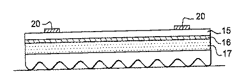
本発明に対応する検出器の他の実施形態を図4及び図5に示す。これはサーモメータ(10)、ダイポール型若しくはダブルダイポール型アンテナ(11,11’)を備え、このアセンブリはアンテナの自由端の近傍にまず形成され、次いでサーモメータのすぐ近傍に形成されたアンカリング点(12)によって浮かされている。繰り返すが、このアセンブリは分離アーム(13)によって基板(2)から熱的に絶縁されている。刺激がサーモメータを通るのを保証するように、これは、酸化シリコンSiO若しくは窒化シリコンSiNから成る単一の誘電層(13)か、又は、例えば窒化チタンTiN(14)から成る抵抗層で頂部に蓋をする誘電層かを備える。 Another embodiment of a detector corresponding to the present invention is shown in FIGS. It comprises a thermometer (10), a dipole or double dipole antenna (11, 11 '), the assembly being first formed near the free end of the antenna and then an anchoring formed in the immediate vicinity of the thermometer Floated by point (12). Again, this assembly is thermally isolated from the substrate (2) by the separating arm (13). In order to ensure that the stimulus passes through the thermometer, it is topped with a single dielectric layer (13) made of silicon oxide SiO or silicon nitride SiN or a resistive layer made of, for example, titanium nitride TiN (14). It is provided with a dielectric layer that covers.
基板は、1μm〜20μmの厚さを有するシリコン層(15)と、3,000Å〜2μmを有する第2の埋込酸化層(例えば、SiO)(16)と、400μm〜500μmの厚さを有する固体基板(17)とを備えたSOI基板である。 The substrate comprises a silicon layer (15) having a thickness of 1 μm to 20 μm, a second buried oxide layer (eg, SiO) (16) having a thickness of 3,000 to 2 μm, and a solid having a thickness of 400 μm to 500 μm. An SOI substrate including a substrate (17).
このアセンブリはλ/4の厚さまでエッチングされて基板(18)に集積される。ここで、λは検出器の作動波長であり、エッチングの底部は好都合には反射器として作用できる導電層(19)で被覆される。 This assembly is etched to a thickness of λ / 4 and integrated on the substrate (18). Where λ is the operating wavelength of the detector and the bottom of the etch is conveniently coated with a conductive layer (19) that can act as a reflector.
この配置は検出器の封入を可能とし、裏面からの照明を要する。 This arrangement allows the detector to be encapsulated and requires illumination from the back side.
本発明のボロメータ検出器の一実施形態を、図6a〜図6eを参照して以下に詳細に説明する。 One embodiment of the bolometer detector of the present invention is described in detail below with reference to FIGS. 6a-6e.
リーダーはまず、ある数の古典的なマイクロエレクトロニクス技術を用いることがリマインドされる。絶縁材料(SiN、SiO、ZnS等)及びアモルファス若しくはポリシリコン半導体(Si,Ge,SiC,a-Si:H,a-SiC:H,a-SiGe:H等)から成る種々のエレメント(0.005μm〜1μm)の薄層の作製は、これらの材料について通常使用されている低温体積法:カソードスパッタリング、低圧化学的気相堆積法(LPCVD)、又は、プラズマ支援化学的気相堆積法(PECVD)を用いて得られる。 Leaders are first reminded to use a number of classic microelectronic technologies. Various elements (0.005 μm) made of insulating materials (SiN, SiO, ZnS, etc.) and amorphous or polysilicon semiconductors (Si, Ge, SiC, a-Si: H, a-SiC: H, a-SiGe: H, etc.) Low temperature volume methods commonly used for these materials: cathode sputtering, low pressure chemical vapor deposition (LPCVD), or plasma assisted chemical vapor deposition (PECVD) Is obtained.
これらの層のいかなるドーピングも、ドーパントガス(BF3、PH3等)をリアクターに導入することによって、又は、イオン注入によって得られる。これらの材料は一般に、プラズマ支援化学エッチング工程によってエッチングされる。 Any doping of these layers can be obtained by introducing a dopant gas (BF3, PH3, etc.) into the reactor or by ion implantation. These materials are typically etched by a plasma assisted chemical etching process.
抵抗エレメント、電極、内部接続のような種々の金属化領域、アンテナ若しくはアンテナ負荷抵抗を成す金属材料(Ti,TiN,Pt,Al,Pd,Ni,NiCr等)は、カソードスパッタリング、LPCVD、又は、PECVDによって堆積される。これらの金属化領域を化学的若しくはプラズマエッチング工程、又は、“リフトオフ”として公知の知られる工程によって画定される。これらの層の厚さは0.005μm〜1μmの範囲である。 Various metallized regions such as resistive elements, electrodes, internal connections, antennas or metal materials that form antenna load resistance (Ti, TiN, Pt, Al, Pd, Ni, NiCr, etc.) can be cathodic sputtering, LPCVD, or Deposited by PECVD. These metallized regions are defined by a chemical or plasma etching process, or a known process known as “lift-off”. The thickness of these layers is in the range of 0.005 μm to 1 μm.
上に支持ポストが形成される金属例えば、アルミウムから成るトラック及びボンディングパッドは、堆積法、フォトリソグラフィ及びエッチングによって初期段階(図6a)中に生成された。これらの層はシリコンから成るスタック(15)、酸化シリコンの埋込層(16)、及び、固体基板(17)上に堆積する。 Tracks and bonding pads made of metal, such as aluminum, on which support posts are formed, were generated during the initial stage (FIG. 6a) by deposition, photolithography and etching. These layers are deposited on a stack of silicon (15), a buried silicon oxide layer (16) and a solid substrate (17).
(図示しない)堆積されたSiO層によるパッシベーション後に、1μm〜10μm厚で例えば、ポリイミドから成る犠牲層が堆積され、次いで、例えば、SiO又はSiNから成る絶縁膜(22)を堆積し、この機能は機械的支持として作用することである。 After passivation with a deposited SiO layer (not shown), a sacrificial layer, for example made of polyimide, is deposited with a thickness of 1 μm to 10 μm, and then an insulating film (22) made of, for example, SiO or SiN is deposited, this function To act as a mechanical support.
一又は二以上の金属層(23,24)(このうちの少なくとも一方は高伝導性(Al,Au))を絶縁膜(22)上に堆積し、まずアンテナを形成し、次いでサーモメータ及びアンテナの負荷抵抗(抵抗金属(TiN、TaN…)から成る)をバイアスするための電極を形成することが意図されている。これらは全て、樹脂マスク(図6b参照)を介してエッチングする。 One or more metal layers (23, 24) (at least one of which is highly conductive (Al, Au)) is deposited on the insulating film (22) to form an antenna first, and then the thermometer and antenna It is intended to form an electrode for biasing the load resistance (consisting of resistance metals (TiN, TaN...)). All of these are etched through a resin mask (see FIG. 6b).
次いで、サーモメータと内部接続との間の電気的コンタクトのベースを構成し、例えばチタン若しくは窒化チタンTiNから成る一又は二以上の金属層(25)を堆積し、そして、エッチングする(図6C)。 It then constitutes the base of the electrical contact between the thermometer and the internal connection, depositing and etching one or more metal layers (25), for example made of titanium or titanium nitride TiN (FIG. 6C). .
第1導電層(25)をアンテナを形成するためにエッチングする。同様に、このような導電層(25)をコンタクト電極を形成するためにエッチングする(図6d参照)。 The first conductive layer (25) is etched to form an antenna. Similarly, such a conductive layer (25) is etched to form a contact electrode (see FIG. 6d).
例えば、アモルファスシリコン若しくは酸化バナジウムから成る熱抵抗材料(6)が堆積され、次いで、サーモメータ領域を保護する樹脂マスクを介してエッチングする。 For example, a thermal resistance material (6) made of amorphous silicon or vanadium oxide is deposited and then etched through a resin mask that protects the thermometer area.
次いで、基板をボッシュ型プラズマ支援化学エッチングでエッチングする(図6e参照)。 Next, the substrate is etched by Bosch type plasma assisted chemical etching (see FIG. 6e).
最後の段階は、犠牲層をエッチングすることによって構造体を切り離すことである。 The last step is to detach the structure by etching the sacrificial layer.
蓋を湿式化学工程によってエッチングできる。(図4に関連して説明した実施形態のように)真空において正面(フロント)上にそれを堆積し若しくは結合する前に、付着層(例えば、チタン)の後に約1μm厚の導電層(Al,Au)をカソードスパッタリングによって堆積される。 The lid can be etched by a wet chemical process. Before depositing or bonding it on the front side (as in the embodiment described in connection with FIG. 4) in vacuum, a conductive layer (Al , Au) is deposited by cathode sputtering.
1 受信アンテナ
2 基板
4 サーモメータ
6 分離アーム
7 アンカリング点
1 receiving antenna 2
Claims (8)
− 収集された電磁波放射を熱に変換できる抵抗負荷(3)と;
− 該抵抗負荷を介して前記受信アンテナに接続され、支持基板(2)から熱的に絶縁されたサーモメータ要素(4)とを備え、前記支持基板(2)が、電気的励起の手段と前記検出器で生成した電気信号を前処理する手段とを含む電子回路を収容できる、電磁波放射用のボロメータ検出器において、
前記受信アンテナが前記支持基板(2)から絶縁されていて、
前記受信アンテナ(1、1’、11’)と、前記抵抗負荷(3)と、前記サーモメータ要素(4)とから成るアセンブリが、前記支持基板上に形成されたアンカリング点(7、12)上に配備された分離アーム(6、13、14)によって前記支持基板の上方に懸架されていて、前記アセンブリを前記支持基板から熱的に絶縁し、
前記分離アーム(6、13)の少なくとも一部が、前記受信アンテナの主要面の自由端上に接続されていることを特徴とする電磁波放射用のボロメータ検出器。 A receiving antenna (1, 1 ′, 11 ′) for collecting electromagnetic radiation;
-A resistive load (3) capable of converting the collected electromagnetic radiation into heat ;
A thermometer element (4) connected to the receiving antenna via the resistive load and thermally insulated from the support substrate (2), the support substrate (2) comprising means for electrical excitation; A bolometer detector for electromagnetic wave radiation , which can accommodate an electronic circuit including means for preprocessing an electrical signal generated by the detector,
The receiving antenna is insulated from the support substrate (2);
An assembly comprising the receiving antenna (1, 1 ′, 11 ′), the resistive load (3), and the thermometer element (4) is an anchoring point (7, 12) formed on the support substrate. ) Suspended above the support substrate by a separating arm (6, 13, 14) disposed thereon to thermally insulate the assembly from the support substrate;
A bolometer detector for electromagnetic wave radiation, wherein at least a part of the separation arm (6, 13) is connected to a free end of a main surface of the receiving antenna.
Applications Claiming Priority (2)
| Application Number | Priority Date | Filing Date | Title |
|---|---|---|---|
| FR0503836A FR2884608B1 (en) | 2005-04-18 | 2005-04-18 | BOLOMETRIC DETECTOR, DEVICE FOR DETECTION OF SUBMILLIMETRIC AND MILLIMETRIC ELECTROMAGNETIC WAVES USING SUCH A DETECTOR |
| FR0503836 | 2005-04-18 |
Publications (2)
| Publication Number | Publication Date |
|---|---|
| JP2006304290A JP2006304290A (en) | 2006-11-02 |
| JP5241077B2 true JP5241077B2 (en) | 2013-07-17 |
Family
ID=35266742
Family Applications (1)
| Application Number | Title | Priority Date | Filing Date |
|---|---|---|---|
| JP2006095481A Expired - Fee Related JP5241077B2 (en) | 2005-04-18 | 2006-03-30 | Bolometer detector and apparatus for detecting submillimeter and millimeter wave electromagnetic waves using the same |
Country Status (6)
| Country | Link |
|---|---|
| US (1) | US7442934B2 (en) |
| EP (1) | EP1715315B1 (en) |
| JP (1) | JP5241077B2 (en) |
| AT (1) | ATE472098T1 (en) |
| DE (1) | DE602006015014D1 (en) |
| FR (1) | FR2884608B1 (en) |
Families Citing this family (21)
| Publication number | Priority date | Publication date | Assignee | Title |
|---|---|---|---|---|
| GB2409337B (en) * | 2002-09-04 | 2005-08-03 | Teraview Ltd | An emitter |
| FI20065776A0 (en) * | 2006-12-05 | 2006-12-05 | Pekka Neittaanmaeki | A method for checking the conductivity of dielectric nanofibers and the corresponding device |
| FR2934044B1 (en) * | 2008-07-17 | 2014-08-15 | Commissariat Energie Atomique | BOLOMETRIC DETECTOR OF ELECTROMAGNETIC WAVES. |
| US8354642B2 (en) * | 2010-10-13 | 2013-01-15 | International Business Machines Corporation | Monolithic passive THz detector with energy concentration on sub-pixel suspended MEMS thermal sensor |
| JP5428783B2 (en) * | 2009-11-12 | 2014-02-26 | 日本電気株式会社 | Bolometer type THz wave detector |
| JP2011237312A (en) * | 2010-05-12 | 2011-11-24 | Hamamatsu Photonics Kk | Terahertz wave detection apparatus and manufacturing method therefor |
| US8570224B2 (en) * | 2010-05-12 | 2013-10-29 | Qualcomm Incorporated | Apparatus providing thermal management for radio frequency devices |
| FR2983952B1 (en) | 2011-12-09 | 2013-11-15 | Commissariat Energie Atomique | BOLOMETRIC DETECTOR FOR ELECTROMAGNETIC RADIATION IN THE FIELD OF TERAHERTZ |
| FR2983953B1 (en) | 2011-12-09 | 2014-01-03 | Commissariat Energie Atomique | BOLOMETRIC DETECTOR OF ELECTROMAGNETIC RADIATION IN THE DOMAIN OF TERAHERTZ AND MATRIX DETECTION DEVICE COMPRISING SUCH DETECTORS |
| RU2511275C2 (en) * | 2012-07-16 | 2014-04-10 | Федеральное государственное унитарное предприятие "Научно-исследовательский институт физических проблем им. Ф.В. Лукина" | Nanostructural ir-receiver (bolometer) with big absorption surface |
| GB2507306A (en) * | 2012-10-25 | 2014-04-30 | Ibm | An antenna-coupled bolometer device for sensing electromagnetic radiation |
| US9052234B2 (en) | 2012-10-30 | 2015-06-09 | International Business Machines Corporation | Dipole antenna with reflectors having low thermal mass for detection of Terahertz radiation |
| US20140117237A1 (en) | 2012-10-30 | 2014-05-01 | International Business Machines Corporation | High responsivity device for thermal sensing in a terahertz radiation detector |
| US8957379B2 (en) | 2012-10-30 | 2015-02-17 | International Business Machines Corporation | Suspended wideband planar skirt antenna having low thermal mass for detection of terahertz radiation |
| US9759693B2 (en) | 2012-12-20 | 2017-09-12 | International Business Machines Corporation | Method of simulating the absorption of plane waves using FEM software tools |
| GB2513170B (en) * | 2013-04-18 | 2020-07-08 | Univ Of Ljubljana | Bolometric detection system with reflecting cavity |
| FR3009865B1 (en) * | 2013-08-22 | 2015-07-31 | Commissariat Energie Atomique | BOLOMETRIC DETECTOR WITH REINFORCED THERMALIZATION COMPENSATION BOLOMETER |
| US20150241281A1 (en) * | 2014-02-27 | 2015-08-27 | International Business Machines Corporation | Bolometer device for sensing electromagnetic radiation |
| JP6486695B2 (en) * | 2015-01-14 | 2019-03-20 | 浜松ホトニクス株式会社 | Bolometer type THz detector |
| CN105371966B (en) * | 2015-11-13 | 2019-01-11 | 南方科技大学 | A kind of novel radiation bolometer and manufacturing method |
| CN111224232B (en) * | 2018-11-23 | 2022-10-18 | 比亚迪股份有限公司 | Dual-band omnidirectional antenna and train |
Family Cites Families (9)
| Publication number | Priority date | Publication date | Assignee | Title |
|---|---|---|---|---|
| JPH0627170A (en) * | 1992-07-08 | 1994-02-04 | Sanyo Electric Co Ltd | Superconducting electromagnetic wave detection element |
| AU1408497A (en) * | 1995-12-04 | 1997-06-27 | Lockheed-Martin Ir Imaging Systems, Inc. | Infrared radiation detector having a reduced active area |
| FI107407B (en) * | 1997-09-16 | 2001-07-31 | Metorex Internat Oy | A submillimeter wave imaging system |
| US6329655B1 (en) * | 1998-10-07 | 2001-12-11 | Raytheon Company | Architecture and method of coupling electromagnetic energy to thermal detectors |
| FR2788129B1 (en) | 1998-12-30 | 2001-02-16 | Commissariat Energie Atomique | BOLOMETRIC DETECTOR WITH ANTENNA |
| US6292140B1 (en) * | 1999-11-03 | 2001-09-18 | Hypres, Inc. | Antenna for millimeter-wave imaging and bolometer employing the antenna |
| FR2845157B1 (en) * | 2002-10-01 | 2004-11-05 | Commissariat Energie Atomique | BOLOMETRIC DETECTOR WITH ANTENNA HAVING A SWITCH AND IMAGING DEVICE COMPRISING SAME. |
| FR2855609B1 (en) * | 2003-05-26 | 2005-07-01 | Commissariat Energie Atomique | OPTIMIZED CAVITY BULOMETRIC ANTENNA DETECTION DEVICE FOR MILLIMETRIC OR SUBMILLIMETRIC ELECTROMAGNETIC WAVES, AND METHOD OF MANUFACTURING THE SAME |
| US7253412B2 (en) * | 2004-10-01 | 2007-08-07 | Northrop Grumman Corporation | Focal plane antenna to sensor interface for an ultra-sensitive silicon sensor |
-
2005
- 2005-04-18 FR FR0503836A patent/FR2884608B1/en not_active Expired - Fee Related
-
2006
- 2006-03-28 EP EP06300295A patent/EP1715315B1/en not_active Not-in-force
- 2006-03-28 AT AT06300295T patent/ATE472098T1/en not_active IP Right Cessation
- 2006-03-28 DE DE602006015014T patent/DE602006015014D1/en active Active
- 2006-03-30 US US11/393,973 patent/US7442934B2/en not_active Expired - Fee Related
- 2006-03-30 JP JP2006095481A patent/JP5241077B2/en not_active Expired - Fee Related
Also Published As
| Publication number | Publication date |
|---|---|
| ATE472098T1 (en) | 2010-07-15 |
| FR2884608A1 (en) | 2006-10-20 |
| EP1715315B1 (en) | 2010-06-23 |
| US7442934B2 (en) | 2008-10-28 |
| EP1715315A1 (en) | 2006-10-25 |
| US20060231761A1 (en) | 2006-10-19 |
| FR2884608B1 (en) | 2007-05-25 |
| DE602006015014D1 (en) | 2010-08-05 |
| JP2006304290A (en) | 2006-11-02 |
Similar Documents
| Publication | Publication Date | Title |
|---|---|---|
| JP5241077B2 (en) | Bolometer detector and apparatus for detecting submillimeter and millimeter wave electromagnetic waves using the same | |
| JP5684487B2 (en) | Bolometer detector for detecting electromagnetic radiation in the infrared to terahertz frequency band, and array detection apparatus having such a detector | |
| USRE36615E (en) | Use of vanadium oxide in microbolometer sensors | |
| JP6084018B2 (en) | Terahertz region electromagnetic radiation bolometer detector and detector array device including the same | |
| US6329655B1 (en) | Architecture and method of coupling electromagnetic energy to thermal detectors | |
| KR100343869B1 (en) | Thermal type infrared ray detector with thermal separation structure for high sensitivity | |
| US7544942B2 (en) | Thermal detector for electromagnetic radiation and infrared detection device using such detectors | |
| US6144030A (en) | Advanced small pixel high fill factor uncooled focal plane array | |
| US6316770B1 (en) | Thermal detector with bolometric effect amplification | |
| US20110057107A1 (en) | Bolometric detector for detecting electromagnetic waves | |
| US6292140B1 (en) | Antenna for millimeter-wave imaging and bolometer employing the antenna | |
| CN107063470B (en) | The detection device of radiation hotting mask is surveyed in suspension with high-selenium corn efficiency and signal-to-noise ratio | |
| US9217674B2 (en) | Bolometric detector of an electromagnetic radiation in the terahertz range and array detection device comprising such detectors | |
| US20150226612A1 (en) | Bolometric detector with a mim structure including a thermometer element | |
| JP2016070935A (en) | Bolometric detector having mim structure of different dimensions | |
| US9052231B2 (en) | Bolometric detector of an electromagnetic radiation in the terahertz range | |
| CA2133081C (en) | Use of abx in microbolometer sensors | |
| KR20230000317A (en) | Bolometer Infrared Sensors to Minimize Output Change Due to High Temperature of Targets | |
| US7541585B2 (en) | Radiant-energy-measuring device with two positions | |
| US20200232913A1 (en) | Infrared device | |
| JP2020532713A (en) | High-speed graphene oxide bolometer and its manufacturing method | |
| KR20230000318A (en) | Method for Manufacturing Bolometer Infrared Sensors to Minimize Output Change Due to High Temperature of Targets |
Legal Events
| Date | Code | Title | Description |
|---|---|---|---|
| A621 | Written request for application examination |
Free format text: JAPANESE INTERMEDIATE CODE: A621 Effective date: 20090108 |
|
| A977 | Report on retrieval |
Free format text: JAPANESE INTERMEDIATE CODE: A971007 Effective date: 20101109 |
|
| A131 | Notification of reasons for refusal |
Free format text: JAPANESE INTERMEDIATE CODE: A131 Effective date: 20101130 |
|
| A601 | Written request for extension of time |
Free format text: JAPANESE INTERMEDIATE CODE: A601 Effective date: 20110228 |
|
| A602 | Written permission of extension of time |
Free format text: JAPANESE INTERMEDIATE CODE: A602 Effective date: 20110303 |
|
| A521 | Request for written amendment filed |
Free format text: JAPANESE INTERMEDIATE CODE: A523 Effective date: 20110407 |
|
| A131 | Notification of reasons for refusal |
Free format text: JAPANESE INTERMEDIATE CODE: A131 Effective date: 20110607 |
|
| A02 | Decision of refusal |
Free format text: JAPANESE INTERMEDIATE CODE: A02 Effective date: 20111004 |
|
| A521 | Request for written amendment filed |
Free format text: JAPANESE INTERMEDIATE CODE: A523 Effective date: 20130208 |
|
| A61 | First payment of annual fees (during grant procedure) |
Free format text: JAPANESE INTERMEDIATE CODE: A61 Effective date: 20130402 |
|
| FPAY | Renewal fee payment (event date is renewal date of database) |
Free format text: PAYMENT UNTIL: 20160412 Year of fee payment: 3 |
|
| R150 | Certificate of patent or registration of utility model |
Free format text: JAPANESE INTERMEDIATE CODE: R150 Ref document number: 5241077 Country of ref document: JP Free format text: JAPANESE INTERMEDIATE CODE: R150 |
|
| R250 | Receipt of annual fees |
Free format text: JAPANESE INTERMEDIATE CODE: R250 |
|
| R250 | Receipt of annual fees |
Free format text: JAPANESE INTERMEDIATE CODE: R250 |
|
| R250 | Receipt of annual fees |
Free format text: JAPANESE INTERMEDIATE CODE: R250 |
|
| LAPS | Cancellation because of no payment of annual fees |