EP1711044A2 - Verfahren zur Übertragung von Bauelementen auf eine Oberfläche - Google Patents
Verfahren zur Übertragung von Bauelementen auf eine Oberfläche Download PDFInfo
- Publication number
- EP1711044A2 EP1711044A2 EP05026243A EP05026243A EP1711044A2 EP 1711044 A2 EP1711044 A2 EP 1711044A2 EP 05026243 A EP05026243 A EP 05026243A EP 05026243 A EP05026243 A EP 05026243A EP 1711044 A2 EP1711044 A2 EP 1711044A2
- Authority
- EP
- European Patent Office
- Prior art keywords
- components
- carrier
- layer
- photoconductor layer
- charge
- Prior art date
- Legal status (The legal status is an assumption and is not a legal conclusion. Google has not performed a legal analysis and makes no representation as to the accuracy of the status listed.)
- Granted
Links
Images

Classifications
-
- H—ELECTRICITY
- H05—ELECTRIC TECHNIQUES NOT OTHERWISE PROVIDED FOR
- H05K—PRINTED CIRCUITS; CASINGS OR CONSTRUCTIONAL DETAILS OF ELECTRIC APPARATUS; MANUFACTURE OF ASSEMBLAGES OF ELECTRICAL COMPONENTS
- H05K3/00—Apparatus or processes for manufacturing printed circuits
- H05K3/30—Assembling printed circuits with electric components, e.g. with resistors
- H05K3/32—Assembling printed circuits with electric components, e.g. with resistors electrically connecting electric components or wires to printed circuits
- H05K3/34—Assembling printed circuits with electric components, e.g. with resistors electrically connecting electric components or wires to printed circuits by soldering
- H05K3/3465—Application of solder
- H05K3/3478—Application of solder preforms; Transferring prefabricated solder patterns
-
- H—ELECTRICITY
- H05—ELECTRIC TECHNIQUES NOT OTHERWISE PROVIDED FOR
- H05K—PRINTED CIRCUITS; CASINGS OR CONSTRUCTIONAL DETAILS OF ELECTRIC APPARATUS; MANUFACTURE OF ASSEMBLAGES OF ELECTRICAL COMPONENTS
- H05K2203/00—Indexing scheme relating to apparatus or processes for manufacturing printed circuits covered by H05K3/00
- H05K2203/03—Metal processing
- H05K2203/0338—Transferring metal or conductive material other than a circuit pattern, e.g. bump, solder, printed component
-
- H—ELECTRICITY
- H05—ELECTRIC TECHNIQUES NOT OTHERWISE PROVIDED FOR
- H05K—PRINTED CIRCUITS; CASINGS OR CONSTRUCTIONAL DETAILS OF ELECTRIC APPARATUS; MANUFACTURE OF ASSEMBLAGES OF ELECTRICAL COMPONENTS
- H05K2203/00—Indexing scheme relating to apparatus or processes for manufacturing printed circuits covered by H05K3/00
- H05K2203/04—Soldering or other types of metallurgic bonding
- H05K2203/041—Solder preforms in the shape of solder balls
-
- H—ELECTRICITY
- H05—ELECTRIC TECHNIQUES NOT OTHERWISE PROVIDED FOR
- H05K—PRINTED CIRCUITS; CASINGS OR CONSTRUCTIONAL DETAILS OF ELECTRIC APPARATUS; MANUFACTURE OF ASSEMBLAGES OF ELECTRICAL COMPONENTS
- H05K2203/00—Indexing scheme relating to apparatus or processes for manufacturing printed circuits covered by H05K3/00
- H05K2203/05—Patterning and lithography; Masks; Details of resist
- H05K2203/0502—Patterning and lithography
- H05K2203/0517—Electrographic patterning
-
- H—ELECTRICITY
- H05—ELECTRIC TECHNIQUES NOT OTHERWISE PROVIDED FOR
- H05K—PRINTED CIRCUITS; CASINGS OR CONSTRUCTIONAL DETAILS OF ELECTRIC APPARATUS; MANUFACTURE OF ASSEMBLAGES OF ELECTRICAL COMPONENTS
- H05K3/00—Apparatus or processes for manufacturing printed circuits
- H05K3/10—Apparatus or processes for manufacturing printed circuits in which conductive material is applied to the insulating support in such a manner as to form the desired conductive pattern
- H05K3/12—Apparatus or processes for manufacturing printed circuits in which conductive material is applied to the insulating support in such a manner as to form the desired conductive pattern using thick film techniques, e.g. printing techniques to apply the conductive material or similar techniques for applying conductive paste or ink patterns
- H05K3/1266—Apparatus or processes for manufacturing printed circuits in which conductive material is applied to the insulating support in such a manner as to form the desired conductive pattern using thick film techniques, e.g. printing techniques to apply the conductive material or similar techniques for applying conductive paste or ink patterns by electrographic or magnetographic printing
-
- H—ELECTRICITY
- H10—SEMICONDUCTOR DEVICES; ELECTRIC SOLID-STATE DEVICES NOT OTHERWISE PROVIDED FOR
- H10W—GENERIC PACKAGES, INTERCONNECTIONS, CONNECTORS OR OTHER CONSTRUCTIONAL DETAILS OF DEVICES COVERED BY CLASS H10
- H10W72/00—Interconnections or connectors in packages
- H10W72/01—Manufacture or treatment
- H10W72/012—Manufacture or treatment of bump connectors, dummy bumps or thermal bumps
- H10W72/01204—Manufacture or treatment of bump connectors, dummy bumps or thermal bumps using temporary auxiliary members, e.g. using sacrificial coatings or handle substrates
Definitions
- the present invention relates to a method for the transmission of components in which components, in particular electrical components or electrical contacting elements, are picked up by a carrier, positioned over a surface and transferred to the surface.
- the present method is used in microtechnology and microsystems technology, in particular in the field of electrical engineering.
- SMD components S urface M ounted D evices
- technical surfaces such as, printed circuits or printed circuit boards
- pick-and-Place 'method by automated assembly devices.
- Such devices generally have at least one movable mounting head.
- the components are picked up by the placement head ("pick") or otherwise fed to it from a component reservoir.
- the placement head positions the components above the technical surface, sets them down and transfers them to the surface ('Place').
- the positioning of the mounting head is usually done using optical methods.
- Such a placement machine is disclosed, for example, in US 5,862,586.
- a disadvantage of the known implementations of the pick-and-place method is that they are not suitable for positioning and transmitting the smallest components with dimensions of the order of 0.5 mm and smaller due to problems with electrostatic charging.
- the mechanical tolerances to be adhered to in the case of corresponding pick-and-place devices are poor or not economically feasible because of the enormous expense associated therewith.
- the invention has for its object to provide a method that low, fast and flexible allows the positioning and transmission of the smallest components, in particular of electrical components with dimensions in the order of 0.5 mm or smaller, on a surface.
- the object is achieved by the method according to claim 1, which describes a method in which diverse components, in particular electrical components or electrical contacting elements, picked up by a carrier, positioned over a technical surface and transferred to the technical surface.
- the invention is based on the idea of structurally electrostatically charging a carrier in such a way that the components to be transferred, due to electrostatic adhesion, adhere to the charge structure applied to the carrier and can be transferred to the technical surface.
- a support to be provided has a photoconductor layer on its surface.
- the carrier itself may consist of different materials and be shaped differently.
- One possibility is the use of flexible tape with appropriate photoconductive coating as a support.
- the photoconductor layer usually consists of a thin, insulating layer on a conductive substrate.
- the photoconductive materials various compounds such as As2Se3, SeTe, ZnO, organic multi-layer devices or amorphous silicon are used.
- the thickness of the photoconductive layer is usually between 10 and 100 ⁇ m.
- the electrostatic charging of the photoconductor layer takes place first.
- One known method for this is that of the coronary discharge.
- a homogeneous surface potential is applied to the photo layer, depending on the photoconductor material and corona voltage up to 900 volts, at a surface charge density of up to 100 nC / cm 2 .
- a charge structure is produced on the photoconductor layer which has a geometry with which the individual components are to be transferred to the technical surface.
- the individual components are preferably imaged in the charge structure as a two-dimensional projection (outline) of the outer three-dimensional shape of the individual components arranged correspondingly. If, for example, a multiplicity of similar spherical contact elements are to be transferred to a technical surface, then a geometrical charge structure is preferably applied to the photoconductor layer which consists of a multiplicity of correspondingly arranged circular charge islands having a diameter equal to the diameter of the spherical contact elements or approximately the same.
- the generation of the charge structure in the initially electrostatically homogeneously charged photoconductor layer takes place in a manner known per se by exposure to a light source of a specific wavelength and energy with or without a mask.
- light sources inter alia, laser come into consideration, since they produce a sharply focused, coherent light beam, but also LEDs can be used.
- the exposure locally causes a discharge of the photoconductor layer and thus, depending on the technique used, a photostructuring of up to 1 ⁇ m resolution. All areas outside the desired charge structure are discharged accordingly. As a result, the desired charge structure differs as charged areas ('charge islands') from the uncharged area outside the structure.
- the components to be transmitted are supplied to the carrier and applied to the now structured electrostatically charged photoconductor layer.
- various techniques are considered, which i.a. depend on the device technology execution and above all on the design of the carrier.
- the components are generally supplied from a corresponding reservoir and distributed on the photoconductor layer such that a component adheres to all of the charge islands provided according to the charge structure due to the electrostatic attraction.
- the components are electrically charged prior to application to the carrier opposite to the surface charge of the photoconductor layer (charge islands).
- the components are coated on one side with a dielectric layer.
- a dielectric layer This leads to a spatially oriented adhesion of the components after the application of the components to the structured charged photoconductor layer.
- a correct alignment (top / bottom) in the transmission of LEDs according to the invention can be ensured by a selective dielectric coating on an LED backside still in the wafer composite.
- components in particular electrical components or contact elements, come into consideration, having dimensions of the order of 0.5 mm and smaller. Due to the magnitude of the electrostatic forces acting on the components in the process, it is only with components of these dimensions that the gravitational forces are compensated by the electrostatic forces.
- Typical applications of the method are the transfer of electrical chips or spherical contact elements, with dimensions on the order of 150 ⁇ m or below, to flip chips, ball grid arrays (BGAs) and chip size packaging (CSPs).
- components come from chemical or biological substances, especially from electrically charged or electrically polarizable substances, such as, proteins, RNA, DNA, into consideration.
- the remaining components i. those components that do not adhere to the cargo islands are removed from the surface of the carrier.
- the removal of the components may be accomplished by the use of mechanical aids, by fluid flows, by the use of gravitational force, by electrostatic, magnetic or electromagnetic forces, or a combination thereof. It makes sense to remove the components removed from the surface of the carrier again to the corresponding component reservoir.
- the adhering to the photoconductor layer of the carrier components transferred to the technical surface.
- the process of transfer can also be assisted by a discharge or reverse charging of the photoconductor layer, so that the components are electrically repelled by the photoconductor layer.
- removal of the carrier for example in the case of roll-to-roll methods known per se, can also take place in such a way that surface points of the photoconductive layer of the carrier and surface points of the technical surface which are initially associated with the process are associated with the method. remove each other.
- the photoconductor layer is electrically discharged after the transmission of the components to the technical surface, so that a repetition of the method with the same carrier is possible.
- a repetition can be used to apply further components to a further technical surface, for example a substrate, or to apply other types of components to the same technical surface.
- the inventive method enables a highly flexible, cost-effective and optimized for high throughput transfer of components to technical surfaces.
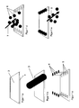
- FIGS. 1 a to 1 i schematically show the individual steps of the method according to the invention during the transfer of spherical contact elements 6 to a technical surface 11.
- Figure 1a shows a carrier 1, which is formed as a quadrangular plate. On the visible, upper surface of the carrier 1, a photoconductor layer 2 is applied.
- FIG. 1b schematically shows the homogeneous, electrostatic charging of the photoconductor layer 2 with a unit (corona) for corona charging 3 of the photoconductor layer 2.
- the corona 3 usually consists of one thin wire, for example made of tungsten, in a housing.
- the white areas represent the applied homogeneous charge distribution 13.
- FIG. 1 c shows the charge structure produced on the carrier 1 by an electrophotographic process.
- a charge structure is produced on the photoconductor layer 2, which has a geometry with which the individual contact elements 6 are to be transferred to the technical surface 11.
- the individual contact elements 6 are imaged in the charge structure as a two-dimensional projection 4 of the outer three-dimensional shape of the individually correspondingly arranged contact elements 6.
- a geometric charge structure is applied to the photoconductor layer 2, which consists of eight correspondingly arranged circular charge islands 5, which have the diameter the spherical contact elements 6 is equal or approximately equal.
- the shaping and dimensioning of the charge islands are possible within certain limits, regardless of the outline of the components. It is essential that the charge islands have a dimensioning such that, on the one hand, the charge pad area is sufficient to ensure electrostatic adhesion only in each case to guarantee a component, and on the other hand, the shape of the charging island leads to an exact positioning of the device on the photoconductor layer.
- FIG. 1d shows the application 7 of the spherical contact elements 6 to the photoconductor layer 2.
- the components are heaped onto the support.
- a variety of other mechanical or electro-mechanical methods and techniques of feeding, applying and distributing components to the photoconductor layer are possible. In principle, it is possible to distinguish between techniques in which the components are supplied in a disordered or ordered manner.
- FIG. 1e illustrates that a contact element 5 adheres to each charge island 5 by electrostatic interactions.
- the removal 8 of all other contact elements 6 is illustrated by the carrier 1. In the simplest case, this is done by simply tilting the carrier. In addition, for example, the use of compressed air or mechanical means for removing all other contact elements is possible.
- FIGS. 1f and 1g illustrate the feeding 9 and positioning 10 of the carrier 1 over the technical surface 11.
- FIG. 1h illustrates the transfer of the contact bodies 6, which adhere to the photoconductor layer 2 of the carrier 1, to the technical surface 11.
- the carrier 1 is brought into operative connection with the technical surface 11 such that after removal 12 (FIG. 1i) of the carrier 1 the adhering to the photoconductor layer 2 contact elements 6 are transferred to the technical surface 11 and placed there or mounted.
Landscapes
- Engineering & Computer Science (AREA)
- Manufacturing & Machinery (AREA)
- Microelectronics & Electronic Packaging (AREA)
- Supply And Installment Of Electrical Components (AREA)
- Photoreceptors In Electrophotography (AREA)
- Manufacturing Of Printed Wiring (AREA)
Abstract
Description
- Die vorliegende Erfindung betrifft ein Verfahren zur Übertragung von Bauelementen, bei dem Bauelemente, insbesondere elektrische Bauelemente oder elektrische Kontaktierelemente, von einem Träger aufgenommen, über einer Oberfläche positioniert und auf die Oberfläche übertragen werden.
- Das vorliegende Verfahren wird in der Mikrotechnologie und Mikrosystemtechnik, insbesondere im Bereich der Elektrotechnik angewendet.
- Das Positionieren und Übertragen von SMD Bauelementen (Surface Mounted Devices) auf technische Oberflächen, wie bspw. gedruckte Schaltungen oder Leiterplatten, wird heute üblicherweise im so genannten 'Pick-and-Place'-Verfahren durch automatisierte Bestückungsvorrichtungen vorgenommen. Derartige Vorrichtungen weisen im Allgemeinen zumindest einen beweglichen Bestückungskopf auf. Die Bauteile werden von dem Bestückungskopf aufgenommen (,Pick') oder ihm anderweitig aus einem Bauteilereservoir zugeführt. Der Bestückungskopf positioniert die Bauteile über der technischen Oberfläche, setzt sie ab und überträgt sie damit auf die Oberfläche (,Place'). Die Positionierung des Bestückungskopfes erfolgt zumeist unter Verwendung optischer Verfahren. Um ein möglichst schnelles Bestücken mit unterschiedlichen Bauelementen zu ermöglichen, weisen moderne Bestückungsvorrichtungen eine Mehrzahl von Bestückungsköpfen auf. Ein solcher Bestückungsautomat ist bspw. in US 5 862 586 offenbart.
- Nachteilig an den bekannten Realisierungen des Pick-and-Place-Verfahrens ist, dass diese sich zur Positionierung und Übertragung kleinster Bauelemente mit Dimensionen in der Größenordnung von 0,5 mm und kleiner aufgrund von Problemen mit elektrostatischen Aufladungen nicht eignen. Zudem sind die dabei einzuhaltenden mechanischen Toleranzen bei entsprechenden Pick-and-Place-Vorrichtungen schlecht oder wegen des damit verbundnen enormen Aufwandes nicht wirtschaftlich realisierbar.
- Darüber hinaus ist die Bestückungsleistung von heute verfügbaren Pick-and-Place Bestückungsverfahren durch die Zahl der gleichzeitig arbeitenden Bestückungsköpfe sowie die Bestückungsleistung der einzelnen Bestückungsköpfe begrenzt.
- Der Erfindung liegt die Aufgabe zugrunde, ein Verfahren anzugeben, das die Positionierung und Übertragung von kleinsten Bauelementen, insbesondere von elektrischen Bauelementen mit Dimensionen in der Größenordnung von 0,5 mm oder kleiner, auf eine Oberfläche günstig, schnell und flexibel ermöglicht.
- Die Aufgabe wird mit dem Verfahren gemäß Patentanspruch 1 gelöst, der ein Verfahren beschreibt, bei dem diverse Bauelemente, insbesondere elektrische Bauelemente oder elektrische Kontaktierelemente, von einem Träger aufgenommen, über einer technischen Oberfläche positioniert und auf die technische Oberfläche übertragen werden.
- Vorteilhafte Ausgestaltungen sind Gegenstand der Unteransprüche sowie der Beschreibung, insbesondere dem Ausführungsbeispiel zu entnehmen.
- Das erfindungsgemäße Verfahren nach dem Oberbegriff des Anspruchs 1 zeichnet sich durch folgende Schritte aus:
- Vorsehen eines elektrostatisch aufladbaren Trägers, der eine Oberfläche mit einer Fotoleiterschicht aufweist,
- Elektrostatisches Aufladen der Fotoleiterschicht des Trägers und Erzeugen einer Ladungsstruktur, die eine Geometrie aufweist, mit der die einzelnen Bauelemente auf die technische Oberfläche übertragen werden sollen,
- Zuführen und Aufbringen der Bauelemente auf die Oberfläche der elektrostatisch geladenen Fotoleiterschicht, wobei nur entsprechend der Ladungsstruktur der Fotoleiterschicht vorgesehene Bauelemente daran haften bleiben,
- Entfernen der übrigen Bauelemente von dem Träger,
- In Kontaktbringen der auf der Fotoleiterschicht haftenden Bauelemente mit der technischen Oberfläche und Übertragen der Bauelemente auf die technische Oberfläche, so, dass nach Entfernen des Trägers die Bauelemente auf die technische Oberfläche übertragen und dort platziert oder montiert sind.
- Die Erfindung basiert auf der Idee einen Träger derart strukturiert elektrostatisch aufzuladen, dass die zu übertragenden Bauelemente aufgrund elektrostatischer Haftung gemäß der auf den Träger aufgebrachten Ladungsstruktur haften bleiben und auf die technische Oberfläche übertragen werden können.
- Erfindungsgemäß weist ein vorzusehender Träger an seiner Oberfläche eine Fotoleiterschicht auf. Der Träger selbst kann je nach Anwendung aus unterschiedlichem Material bestehen und unterschiedlich geformt sein. Eine Möglichkeit bietet die Verwendung von flexiblem Band mit entsprechender fotoleitender Beschichtung als Träger. Als besonders sinnvoll für die gerätetechnische Umsetzung des Verfahrens sind ebene, plattenförmige Träger oder Träger die eine Zylinderform aufweisen aus Metall, bspw. Aluminium. Die Fotoleiterschicht besteht üblicherweise aus einer dünnen, isolierenden Schicht auf einem leitenden Substrat. Als fotoleitende Materialien kommen verschiedene Stoffverbindungen wie bspw. As2Se3, SeTe, ZnO, organische Mehrschichtanordnungen oder amorphes Silizium zur Anwendung. Die Dicke der Fotoleiterschicht liegt üblicherweise zwischen 10 - 100 µm.
- In dem zweiten Verfahrensschritt erfolgt zunächst das elektrostatische Aufladen der Fotoleiterschicht. Ein bekanntes Verfahren hierzu ist das der Koronarentladung. Damit wird auf die Fotoschicht ein homogenes Oberflächenpotential aufgebracht, das je nach Fotoleitermaterial und Koronarspannung bis zu 900 Volt, bei einer Oberflächenladungsdichte von bis zu 100 nC/cm2 betragen kann.
- Nach der homogenen Aufladung wird auf der Fotoleiterschicht eine Ladungsstruktur erzeugt, die eine Geometrie aufweist, mit der die einzelnen Bauelemente auf die technische Oberfläche übertragen werden sollen. Die einzelnen Bauelemente werden dabei in der Ladungsstruktur vorzugsweise als zwei-dimensionale Projektion (Umriss) der äußeren dreidimensionalen Form der einzelnen entsprechend angeordneten Bauelemente abgebildet. Gilt es bspw. eine Vielzahl von gleichartigen kugelförmigen Kontaktelementen auf eine technische Oberfläche zu übertragen, so wird vorzugsweise eine geometrische Ladungsstruktur auf die Fotoleiterschicht aufgebracht, die aus einer Vielzahl entsprechend angeordneter kreisförmiger Ladungsinseln besteht, die einen Durchmesser aufweisen, der dem Durchmesser der kugelförmigen Kontaktelemente gleich oder annähernd gleich ist.
- Das Erzeugen der Ladungsstruktur in der zunächst elektrostatisch homogen geladenen Fotoleiterschicht erfolgt in an sich bekannter Weise durch Belichtung mit einer Lichtquelle bestimmter Wellenlänge und Energie mit oder ohne einer Maske. Als Lichtquellen kommen unter anderem Laser in Betracht, da sie einen scharf gebündelten, kohärenten Lichtstrahl erzeugen, aber auch LED's können zum Einsatz kommen. Die Belichtung bewirkt lokal eine Entladung der Fotoleiterschicht und damit je nach eingesetzter Technik eine Fotostrukturierung von bis zu 1 µm Auflösung. Alle Bereiche außerhalb der gewünschten Ladungsstruktur werden dementsprechend entladen. Demzufolge unterscheidet sich die gewünschte Ladungsstruktur als geladene Bereiche (,Ladungsinseln') von dem ungeladenen Bereich außerhalb der Struktur.
- Im dritten Verfahrensschritt werden die zu übertragenden Bauelemente dem Träger zugeführt und auf die nun strukturiert elektrostatisch geladene Fotoleiterschicht aufgebracht. Für das Zuführen der Bauelemente kommen verschiedene Techniken in Betracht, die u.a. von der gerätetechnischen Ausführung und vor allem von der Gestaltung des Trägers abhängen. Die Bauelemente werden im Allgemeinen aus einem entsprechenden Reservoir zugeführt und auf der Fotoleiterschicht derart verteilt, dass an allen entsprechend der Ladungsstruktur vorgesehenen Ladungsinseln aufgrund der elektrostatischen Anziehung ein Bauelement haften bleibt.
- In einer vorteilhaften Ausbildung des Verfahrens werden die Bauelemente vor dem Aufbringen auf den Träger entgegengesetzt zur Oberflächenladung der Fotoleiterschicht (Ladungsinseln) elektrisch aufgeladen.
- In einer weiteren vorteilhaften Ausbildung des Verfahrens sind die Bauelemente an einer Seite mit einer dielektrischen Schicht beschichtet. Dies führt nach dem Aufbringen der Bauelemente auf die strukturiert geladene Fotoleiterschicht zu einem räumlich ausgerichteten Anhaften der Bauelemente. Beispielsweise kann durch eine selektive dielektrische Beschichtung auf einer LED-Rückseite noch im Waferverbund eine korrekte Ausrichtung (oben/ unten) bei der erfindungsgemäßen Übertragung von LED's sichergestellt werden.
- Idealerweise werden bei einem Verfahrensdurchgang identische Bauelemente verwendet. Es kommen dabei Bauelemente, insbesondere elektrische Bau- oder Kontaktelemente, in Betracht, die Dimensionen in der Größenordnung von 0,5 mm und kleiner aufweisen. Aufgrund der Größenordnung der im Verfahren auf die Bauelemente wirkenden elektrostatischen Kräfte, kommt es erst bei Bauteilen dieser Dimensionen zu einer Kompensation der Gravitationskräfte durch die elektrostatischen Kräfte. Typische Anwendungen des Verfahrens sind das Übertragen von elektrischen Chips oder kugelförmigen Kontaktelementen, so genannten 'Contact-Balls', mit Dimensionen in der Größenordnung von 150 µm oder darunter auf Flip Chips, BGA's (Ball Grid Array's) und CSP's (Chip Size Packaging). Darüber hinaus kommen auch Bauelemente aus chemischen oder biologischen Substanzen, vor allem aus elektrisch geladenen oder elektrisch polarisierbaren Substanzen, wie bspw. Proteine, RNA, DNA, in Betracht.
- Im vierten Verfahrensschritt werden die übrigen Bauelemente, d.h. diejenigen Bauelemente die nicht an den Ladungsinseln haften, von der Oberfläche des Trägers entfernt. Das Entfernen der Bauelemente kann durch den Einsatz mechanischer Hilfsmittel, durch Fluidströme, durch Nutzung der Gravitationskraft, von elektrostatischen, magnetischen oder elektromagnetischen Kräften oder einer Kombination daraus erfolgen. Sinnvollerweise werden die von der Oberfläche des Trägers entfernten Bauelemente wieder dem entsprechenden Bauelementereservoir zugeführt.
- Im fünften und letzten Verfahrensschritt werden die an der Fotoleiterschicht des Trägers haftenden Bauelemente auf die technische Oberfläche übertragen. Dabei wird abhängig von der gerätetechnischen Realisierung ggf. zunächst der Träger über der technischen Oberfläche positioniert. Anschließend wird der Träger mit der technischen Oberfläche in Wirkverbindung gebracht, so dass nach Entfernen des Trägers die an dessen Fotoleiterschicht haftenden Bauelemente auf die technische Oberfläche übertragen, platziert oder montiert sind.
- In einer weiteren Ausbildung des Verfahrens kann der Vorgang des Übertragens zudem durch eine Entladung oder gegenpolige Aufladung der Fotoleiterschicht unterstützt werden, so dass die Bauelemente von der Fotoleiterschicht elektrisch abgestoßen werden.
- Je nach gerätetechnischer Realisierung kann das Entfernen des Trägers, bspw. im Fall von an sich bekannten Rolle-Rolle-Verfahren, auch derart erfolgen, dass sich im Verfahren zugeordnete Oberflächenpunkte von Fotoleiterschicht des Trägers und Oberflächenpunkte der technischen Oberfläche, die zunächst in Wirkverbindung stehen, voneinander entfernen.
- Bei einer weiteren vorteilhaften Weiterbildung des Verfahrens wird die Fotoleiterschicht nach der Übertragung der Bauelemente auf die technische Oberfläche elektrisch entladen, so dass eine Wiederholung des Verfahrens mit demselben Träger möglich ist. Eine derartige Wiederholung kann genutzt werden, um weitere Bauteile auf eine weitere technische Oberfläche, bspw. ein Substrat, aufzubringen oder um andersartige Bauteile auf dieselbe technische Oberfläche aufzubringen.
- Das erfindungsgemäße Verfahren ermöglicht ein hochflexibles, kostengünstiges und auf hohen Durchsatz optimiertes Übertragen von Bauelementen auf technische Oberflächen.
- Die Erfindung wird nachstehend ohne Beschränkung des allgemeinen Erfindungsgedankens anhand von Ausführungsbeispielen und unter Bezugnahme auf die Zeichnungen exemplarisch beschrieben. Dabei zeigen:
- Fig. 1a-i
- Schematische Darstellung der Verfahrensschritte bei der Übertragung von kugelförmigen Kontaktelementen auf eine technische Oberfläche bei einem Platte-Platte-Verfahren.
- Die Figuren 1 a bis 1 i zeigen schematisch die einzelnen Schritte des erfindungsgemäßen Verfahrens bei einem Übertragen von kugelförmigen Kontaktelementen 6 auf eine technische Oberfläche 11.
- Figur 1a zeigt einen Träger 1, der als viereckige Platte ausgebildet ist. Auf der sichtbaren, oben liegenden Oberfläche des Trägers 1 ist eine Fotoleiterschicht 2 aufgebracht.
- Figur 1b zeigt schematisch das homogene, elektrostatische Aufladen der Fotoleiterschicht 2 mit einer Einheit (Korona) zur Koronaraufladung 3 der Fotoleiterschicht 2. Üblicherweise besteht die Korona 3 aus einem dünnen Draht, bspw. aus Wolfram, in einem Gehäuse. Die weißen Flächen repräsentieren dabei die aufgebrachte homogene Ladungsverteilung 13.
- Figur 1c zeigt die durch ein elektrofotografisches Verfahren auf dem Träger 1 erzeugte Ladungsstruktur. Nach der homogenen Aufladung wird auf der Fotoleiterschicht 2 eine Ladungsstruktur erzeugt, die eine Geometrie aufweist, mit der die einzelnen Kontaktelemente 6 auf die technische Oberfläche 11 übertragen werden sollen. In dem vorliegenden Fall sollen jeweils zwei mal vier kugelförmige Kontaktelemente 6 übertragen werden, wobei jeweils vier Kontaktelemente 6 an den abgebildeten Positionen (weiße Kreise) des Trägers 1 nebeneinander in Reihe angeordnet werden sollen. Die einzelnen Kontaktelemente 6 werden dabei in der Ladungsstruktur als zwei-dimensionalen Projektion 4 der äußeren dreidimensionalen Form der einzelnen entsprechend angeordneten Kontaktelemente 6 abgebildet. Gilt es, wie im vorliegenden Ausführungsbeispiel, acht gleichartige kugelförmige Kontaktelemente 6 auf eine technische Oberfläche 11 zu übertragen, so wird eine geometrische Ladungsstruktur auf die Fotoleiterschicht 2 aufgebracht, die aus acht entsprechend angeordneten kreisförmigen Ladungsinseln 5 besteht, die einen Durchmesser aufweisen, der dem Durchmesser der kugelförmigen Kontaktelemente 6 gleich oder annähernd gleich ist. Allerdings sind die Formgebung und die Dimensionierung der Ladungsinseln in gewissen Grenzen auch unabhängig vom Umriss der Bauelemente möglich. Wesentlich dabei ist, dass die Ladungsinseln eine Dimensionierung derart aufweisen, dass einerseits die Ladungsinselfläche ausreicht, um ein elektrostatisches Anhaften nur jeweils eines Bauelements zu garantieren, und dass andererseits die Formgebung der Ladungsinsel zu einer exakten Positionierung des Bauelementes auf der Fotoleiterschicht führt.
- Durch die Belichtung der Fotoleiterschicht 2 wurden alle Bereiche der Fotoleiterschicht 2 entladen, die außerhalb der zweidimensionalen Projektion 5 der zu übertragenden Kontaktelemente 6 liegen.
- Figur 1d zeigt das Aufbringen 7 der kugelförmigen Kontaktelemente 6 auf die Fotoleiterschicht 2. In der hier gezeigten Figur ist angedeutet, dass die Bauelemente auf den Träger aufgeschüttet werden. Darüber hinaus sind eine Vielzahl von weiteren mechanischen oder elektromechanischen Methoden und Techniken des Zuführens, Aufbringens und Verteilens von Bauelementen auf die Fotoleiterschicht möglich. Grundsätzlich kann dabei zwischen Techniken unterschieden werden, bei denen die Bauelemente ungeordnet oder geordnet zugeführt werden.
- Figur 1e veranschaulicht, dass durch elektrostatische Wechselwirkungen an jeder Ladungsinsel 5 ein Kontaktelement 5 haftet. Darüber hinaus wird das Entfernen 8 aller übrigen Kontaktelemente 6 vom Träger 1 veranschaulicht. Im einfachsten Fall geschieht dies durch einfaches Kippen des Trägers. Darüber hinaus ist bspw. der Einsatz von Druckluft oder mechanischer Mittel zur Entfernung aller übrigen Kontaktelemente möglich.
- Die Figuren 1f und 1g veranschaulichen das Zuführen 9 und Positionieren 10 des Trägers 1 über der technischen Oberfläche 11.
- Figur 1h veranschaulicht das Übertragen der Kontaktkörper 6, die an der Fotoleiterschicht 2 des Trägers 1 haften, auf die technische Oberfläche 11. Dabei wird der Träger 1 mit der technischen Oberfläche 11 derart in Wirkverbindung gebracht, dass nach Entfernen 12 (Figur 1i) des Trägers 1 die an dessen Fotoleiterschicht 2 haftenden Kontaktelemente 6 auf die technische Oberfläche 11 übertragen und dort platziert oder montiert sind.
-
- 1
- Träger
- 2
- Fotoleiterschicht
- 3
- Korona, Einheit zur Koronaraufladung
- 4
- 2-dimensionale Projektion eines 3-dimensionalen Kontaktelements
- 5
- Ladungsinsel
- 6
- Kontaktelemente
- 7
- Aufbringen von Kontaktelementen auf die Fotoleiterschicht
- 8
- Entfernen überschüssiger Kontaktelemente vom Träger
- 9
- Zuführen des Trägers zur technischen Oberfläche
- 10
- Positionieren des Trägers relativ zur technischen Oberfläche
- 11
- Technische Oberfläche eines steifen, starren Substrats
- 12
- Entfernen des Trägers von der technischen Oberfläche
Claims (15)
- Verfahren zur Übertragung von Bauelementen, bei dem Bauelemente (6), insbesondere elektrische Bauelemente oder elektrische Kontaktierelemente, von einem Träger (1) aufgenommen, über einer Oberfläche (11) positioniert und auf die Oberfläche (11) übertragen werden, gekennzeichnet durch folgende Schritte:- Vorsehen eines elektrostatisch aufladbaren Trägers (1), der eine Oberfläche mit einer Fotoleiterschicht (2)aufweist,- Elektrostatisches Aufladen der Fotoleiterschicht (2) des Trägers (1) und Erzeugen einer Ladungsstruktur, die eine Geometrie aufweist, mit der die einzelnen Bauelemente (1) auf die Oberfläche (11) übertragen werden sollen,- Zuführen und Aufbringen der Bauelemente (6) auf die Oberfläche der elektrostatisch geladenen Fotoleiterschicht (2), wobei nur entsprechend der Ladungsstruktur der Fotoleiterschicht (2) vorgesehene Bauelemente (6) daran haften bleiben,- Entfernen der übrigen Bauelemente (6) von dem Träger (1),- In Kontaktbringen der auf der Fotoleiterschicht (2) haftenden Bauelemente (6) mit der Oberfläche (11) und Übertragen der Bauelemente (6) auf die Oberfläche (11).
- Verfahren nach Anspruch 1,
dadurch gekennzeichnet, dass identische Bautelemente(6) verwendet werden. - Verfahren nach einem der Ansprüche 1 bis 2,
dadurch gekennzeichnet, dass das elektrostatische Aufladen der Fotoleiterschicht (2) mittels einer Koronaaufladung erfolgt. - Verfahren nach einem der Ansprüche 1 bis 3,
dadurch gekennzeichnet, dass das Erzeugen der Ladungsstruktur durch Belichten der Fotoleiterschicht (2) erfolgt. - Verfahren nach einem der Ansprüche 1 bis 4,
dadurch gekennzeichnet, dass das Erzeugen der Ladungsstruktur durch ein elektrofotografisches Verfahren erfolgt. - Verfahren nach einem der Ansprüche 1 bis 5,
dadurch gekennzeichnet, dass die Bauelemente (6) vor dem Aufbringen auf den Träger (1) entgegengesetzt zur Oberflächenladung der strukturiert geladenen Fotoschicht (2) elektrisch aufgeladen werden. - Verfahren nach einem der Ansprüche 1 bis 6,
dadurch gekennzeichnet, dass durch selektives Beschichten der Bauelemente (6) mit einer dielelektrischen Schicht ein ausgerichtetes Anhaften der Bauelemente (6) an dem Träger (1) erfolgt. - Verfahren nach einem der Ansprüche 1 bis 7,
dadurch gekennzeichnet, dass das Entfernen der Bauelemente (6) mittels der auf die Bauelemente (6) wirkenden Gravitationskraft erfolgt. - Verfahren nach einem der Ansprüche 1 bis 8,
dadurch gekennzeichnet, dass das Entfernen der Bauelemente (6) mittels eines Fluidstromes erfolgt. - Verfahren nach einem der Ansprüche 1 bis 9,
dadurch gekennzeichnet, dass vor dem in Kontaktbringen ein Positionieren und Ausrichten des Trägers (1) relativ zur Oberfläche (11) erfolgt. - Verfahren nach einem der Ansprüche 1 bis 10,
dadurch gekennzeichnet, dass beim Übertragen der Bauelemente (6) auf die Oberfläche (11), die Fotoleiterschicht (2) entladen oder gegenpolig aufgeladen wird. - Verfahren nach einem der Ansprüche 1 bis 11,
dadurch gekennzeichnet, dass nach dem Übertragen der Bauelemente (6) auf die Oberfläche (11) die Fotoleiterschicht (2) entladen wird. - Verfahren zur Übertragung von Bauelementen, bei dem durch wiederholtes Anwenden des Verfahrens nach einem der Ansprüche 1 bis 12 auf eine Oberfläche (11) unterschiedliche Bauelemente (6) aufgebracht werden.
- Verwendung des Verfahrens nach einem der Ansprüche 1 bis 13, zur Positionierung und Übertragung von kugelförmige Kontaktelementen (6) oder elektrischen Chips auf eine Oberfläche, insbesondere eine Leiterplatte.
- Verwendung des Verfahrens nach einem der Ansprüche 1 bis 13, zur Positionierung und Übertragung von Kontaktelementen (6), insbesondere von Contact-Balls, auf Flip Chips, BGA's (Ball Grid Array's) und CSP's (Chip Size Packaging).
Applications Claiming Priority (1)
| Application Number | Priority Date | Filing Date | Title |
|---|---|---|---|
| DE102004058201A DE102004058201A1 (de) | 2004-12-02 | 2004-12-02 | Verfahren zur Übertragung von Bauelementen auf eine Oberfläche |
Publications (3)
| Publication Number | Publication Date |
|---|---|
| EP1711044A2 true EP1711044A2 (de) | 2006-10-11 |
| EP1711044A3 EP1711044A3 (de) | 2008-07-09 |
| EP1711044B1 EP1711044B1 (de) | 2013-05-22 |
Family
ID=36051382
Family Applications (1)
| Application Number | Title | Priority Date | Filing Date |
|---|---|---|---|
| EP05026243.5A Expired - Lifetime EP1711044B1 (de) | 2004-12-02 | 2005-12-01 | Verfahren zur Übertragung von elektrischen Bauelementen auf eine Oberfläche |
Country Status (2)
| Country | Link |
|---|---|
| EP (1) | EP1711044B1 (de) |
| DE (1) | DE102004058201A1 (de) |
Families Citing this family (2)
| Publication number | Priority date | Publication date | Assignee | Title |
|---|---|---|---|---|
| DE102006016275B4 (de) * | 2006-03-31 | 2013-12-19 | Asm Assembly Systems Gmbh & Co. Kg | Verfahren zum Platzieren von elektrisch kontaktierbaren Bauelementen auf einem Schaltungsträger |
| DE102006017359B3 (de) * | 2006-04-11 | 2007-12-20 | Schott Ag | Verkapselung elektronischer und optoelektronischer Bauteile im Waferverbund |
Family Cites Families (4)
| Publication number | Priority date | Publication date | Assignee | Title |
|---|---|---|---|---|
| DE3808667A1 (de) * | 1988-03-15 | 1989-10-05 | Siemens Ag | Montageverfahren zur herstellung von led-zeilen |
| JP2003046222A (ja) * | 2001-07-31 | 2003-02-14 | Matsushita Electric Ind Co Ltd | 接合材料およびその製造方法 |
| JP2003178624A (ja) * | 2001-12-12 | 2003-06-27 | Idemitsu Kosan Co Ltd | 樹脂被膜金属粒子、接合材料、電子回路基板及びそれらの製造方法 |
| JP2006345701A (ja) * | 2003-07-01 | 2006-12-28 | Taisho Pharmaceut Co Ltd | タキサン類応答性の判別方法 |
-
2004
- 2004-12-02 DE DE102004058201A patent/DE102004058201A1/de not_active Ceased
-
2005
- 2005-12-01 EP EP05026243.5A patent/EP1711044B1/de not_active Expired - Lifetime
Also Published As
| Publication number | Publication date |
|---|---|
| EP1711044B1 (de) | 2013-05-22 |
| DE102004058201A1 (de) | 2006-06-22 |
| EP1711044A3 (de) | 2008-07-09 |
Similar Documents
| Publication | Publication Date | Title |
|---|---|---|
| DE69719882T2 (de) | Abtrennungsverfahren für Platten und Vorrichtung zur Durchführung dieses Verfahrens | |
| DE69332196T2 (de) | Verfahren zum Spritzgiessen von Lot und deren Anwendung | |
| KR100377603B1 (ko) | 이방전도성수지필름 | |
| WO1999030168A1 (de) | Vorrichtung und verfahren zur elektrisch ausgelösten mikrotropfenabgabe mit einem dispensierkopf | |
| DE102013208446A1 (de) | Optische Baugruppe | |
| EP0404789B1 (de) | Montageverfahren zur herstellung von led-zeilen | |
| DE102015201998A1 (de) | Kameramodul sowie Verfahren zur Herstellung | |
| WO2003028416A1 (de) | Verfahren zur herstellung einer strukturierten metallschicht auf einem trägerkörper und trägerkörper mit einer strukturierten metallschicht | |
| DE102004025279B4 (de) | Anlage für ein Bestücken von Substraten mit Kugelkontakten und Verfahren zum Bestücken von Substraten mit Kugelkontakten | |
| EP1711044B1 (de) | Verfahren zur Übertragung von elektrischen Bauelementen auf eine Oberfläche | |
| DE10051466C2 (de) | Anordnung als Maske für Lithographie | |
| JP3120112B2 (ja) | 微小物の精密配置法 | |
| DE10254927B4 (de) | Verfahren zur Herstellung von leitfähigen Strukturen auf einem Träger und Verwendung des Verfahrens | |
| DE4434917C1 (de) | Verfahren zum selektiven Aufbringen von Klebstoff | |
| DE102017120210A1 (de) | Verfahren zur Herstellung eines Schichtenabfolgenelements sowie Schichtenabfolgenelement für die Herstellung eines dielektrischen Elastomerwandlers | |
| WO2007113139A1 (de) | Verfahren zum platzieren von elektrisch kontaktierbaren bauelementen auf einem schaltungsträger sowie zur durchführung dieses verfahrens geeignetes montagesystem | |
| WO2000002264A1 (de) | Mikrosystem und verfahren zur herstellung | |
| WO2007113182A1 (de) | Verfahren zum aufbringen von lotpartikeln auf kontaktflächen sowie hierfür geeignete lotpartikel und bauteile mit kontaktflächen | |
| DE10258094B4 (de) | Verfahren zur Ausbildung von 3-D Strukturen auf Wafern | |
| DE102024200400B4 (de) | Vorrichtung und Verfahren zum Herstellen eines Bauteils | |
| DE10258798A1 (de) | Verfahren und Vorrichtung zum partiellen Aufbringen von Klebstoff auf elektronische Bauelemente, Bestückvorrichtung zum Bestücken von Bauelementen | |
| EP3761349B1 (de) | Verfahren zur herstellung von halbleiterbauelementen zur ausbeutesteigerung beim mikrotransferdruck | |
| DE102005005801B4 (de) | Elektrostatisches Ablenksystem für Korpuskularstrahlung | |
| DE10258801A1 (de) | Verfahren und Vorrichtung zum Aufbringen eines pastenartigen Materials auf elektronische Bauelemente, Bestückvorrichtung | |
| WO2001083230A1 (de) | Verfahren zur verbesserung der druckqualität beim einsatz von druckschablonen |
Legal Events
| Date | Code | Title | Description |
|---|---|---|---|
| PUAI | Public reference made under article 153(3) epc to a published international application that has entered the european phase |
Free format text: ORIGINAL CODE: 0009012 |
|
| AK | Designated contracting states |
Kind code of ref document: A2 Designated state(s): AT BE BG CH CY CZ DE DK EE ES FI FR GB GR HU IE IS IT LI LT LU LV MC NL PL PT RO SE SI SK TR |
|
| AX | Request for extension of the european patent |
Extension state: AL BA HR MK YU |
|
| PUAL | Search report despatched |
Free format text: ORIGINAL CODE: 0009013 |
|
| RIC1 | Information provided on ipc code assigned before grant |
Ipc: H05K 3/34 20060101ALI20080529BHEP Ipc: H05K 13/04 20060101AFI20060906BHEP |
|
| AK | Designated contracting states |
Kind code of ref document: A3 Designated state(s): AT BE BG CH CY CZ DE DK EE ES FI FR GB GR HU IE IS IT LI LT LU LV MC NL PL PT RO SE SI SK TR |
|
| AX | Request for extension of the european patent |
Extension state: AL BA HR MK YU |
|
| 17P | Request for examination filed |
Effective date: 20081217 |
|
| 17Q | First examination report despatched |
Effective date: 20090130 |
|
| AKX | Designation fees paid |
Designated state(s): AT BE BG CH CY CZ DE DK EE ES FI FR GB GR HU IE IS IT LI LT LU LV MC NL PL PT RO SE SI SK TR |
|
| GRAP | Despatch of communication of intention to grant a patent |
Free format text: ORIGINAL CODE: EPIDOSNIGR1 |
|
| GRAS | Grant fee paid |
Free format text: ORIGINAL CODE: EPIDOSNIGR3 |
|
| GRAA | (expected) grant |
Free format text: ORIGINAL CODE: 0009210 |
|
| AK | Designated contracting states |
Kind code of ref document: B1 Designated state(s): AT BE BG CH CY CZ DE DK EE ES FI FR GB GR HU IE IS IT LI LT LU LV MC NL PL PT RO SE SI SK TR |
|
| REG | Reference to a national code |
Ref country code: GB Ref legal event code: FG4D Free format text: NOT ENGLISH |
|
| REG | Reference to a national code |
Ref country code: CH Ref legal event code: EP |
|
| REG | Reference to a national code |
Ref country code: AT Ref legal event code: REF Ref document number: 613777 Country of ref document: AT Kind code of ref document: T Effective date: 20130615 |
|
| REG | Reference to a national code |
Ref country code: IE Ref legal event code: FG4D Free format text: LANGUAGE OF EP DOCUMENT: GERMAN |
|
| REG | Reference to a national code |
Ref country code: DE Ref legal event code: R096 Ref document number: 502005013720 Country of ref document: DE Effective date: 20130718 |
|
| REG | Reference to a national code |
Ref country code: LT Ref legal event code: MG4D |
|
| PG25 | Lapsed in a contracting state [announced via postgrant information from national office to epo] |
Ref country code: PT Free format text: LAPSE BECAUSE OF FAILURE TO SUBMIT A TRANSLATION OF THE DESCRIPTION OR TO PAY THE FEE WITHIN THE PRESCRIBED TIME-LIMIT Effective date: 20130923 Ref country code: SI Free format text: LAPSE BECAUSE OF FAILURE TO SUBMIT A TRANSLATION OF THE DESCRIPTION OR TO PAY THE FEE WITHIN THE PRESCRIBED TIME-LIMIT Effective date: 20130522 Ref country code: LT Free format text: LAPSE BECAUSE OF FAILURE TO SUBMIT A TRANSLATION OF THE DESCRIPTION OR TO PAY THE FEE WITHIN THE PRESCRIBED TIME-LIMIT Effective date: 20130522 Ref country code: IS Free format text: LAPSE BECAUSE OF FAILURE TO SUBMIT A TRANSLATION OF THE DESCRIPTION OR TO PAY THE FEE WITHIN THE PRESCRIBED TIME-LIMIT Effective date: 20130922 Ref country code: ES Free format text: LAPSE BECAUSE OF FAILURE TO SUBMIT A TRANSLATION OF THE DESCRIPTION OR TO PAY THE FEE WITHIN THE PRESCRIBED TIME-LIMIT Effective date: 20130902 Ref country code: SE Free format text: LAPSE BECAUSE OF FAILURE TO SUBMIT A TRANSLATION OF THE DESCRIPTION OR TO PAY THE FEE WITHIN THE PRESCRIBED TIME-LIMIT Effective date: 20130522 Ref country code: GR Free format text: LAPSE BECAUSE OF FAILURE TO SUBMIT A TRANSLATION OF THE DESCRIPTION OR TO PAY THE FEE WITHIN THE PRESCRIBED TIME-LIMIT Effective date: 20130823 Ref country code: FI Free format text: LAPSE BECAUSE OF FAILURE TO SUBMIT A TRANSLATION OF THE DESCRIPTION OR TO PAY THE FEE WITHIN THE PRESCRIBED TIME-LIMIT Effective date: 20130522 |
|
| REG | Reference to a national code |
Ref country code: NL Ref legal event code: VDEP Effective date: 20130522 |
|
| PG25 | Lapsed in a contracting state [announced via postgrant information from national office to epo] |
Ref country code: PL Free format text: LAPSE BECAUSE OF FAILURE TO SUBMIT A TRANSLATION OF THE DESCRIPTION OR TO PAY THE FEE WITHIN THE PRESCRIBED TIME-LIMIT Effective date: 20130522 Ref country code: BG Free format text: LAPSE BECAUSE OF FAILURE TO SUBMIT A TRANSLATION OF THE DESCRIPTION OR TO PAY THE FEE WITHIN THE PRESCRIBED TIME-LIMIT Effective date: 20130822 |
|
| PG25 | Lapsed in a contracting state [announced via postgrant information from national office to epo] |
Ref country code: LV Free format text: LAPSE BECAUSE OF FAILURE TO SUBMIT A TRANSLATION OF THE DESCRIPTION OR TO PAY THE FEE WITHIN THE PRESCRIBED TIME-LIMIT Effective date: 20130522 |
|
| PG25 | Lapsed in a contracting state [announced via postgrant information from national office to epo] |
Ref country code: CZ Free format text: LAPSE BECAUSE OF FAILURE TO SUBMIT A TRANSLATION OF THE DESCRIPTION OR TO PAY THE FEE WITHIN THE PRESCRIBED TIME-LIMIT Effective date: 20130522 Ref country code: SK Free format text: LAPSE BECAUSE OF FAILURE TO SUBMIT A TRANSLATION OF THE DESCRIPTION OR TO PAY THE FEE WITHIN THE PRESCRIBED TIME-LIMIT Effective date: 20130522 Ref country code: DK Free format text: LAPSE BECAUSE OF FAILURE TO SUBMIT A TRANSLATION OF THE DESCRIPTION OR TO PAY THE FEE WITHIN THE PRESCRIBED TIME-LIMIT Effective date: 20130522 Ref country code: EE Free format text: LAPSE BECAUSE OF FAILURE TO SUBMIT A TRANSLATION OF THE DESCRIPTION OR TO PAY THE FEE WITHIN THE PRESCRIBED TIME-LIMIT Effective date: 20130522 |
|
| PG25 | Lapsed in a contracting state [announced via postgrant information from national office to epo] |
Ref country code: IT Free format text: LAPSE BECAUSE OF FAILURE TO SUBMIT A TRANSLATION OF THE DESCRIPTION OR TO PAY THE FEE WITHIN THE PRESCRIBED TIME-LIMIT Effective date: 20130522 Ref country code: NL Free format text: LAPSE BECAUSE OF FAILURE TO SUBMIT A TRANSLATION OF THE DESCRIPTION OR TO PAY THE FEE WITHIN THE PRESCRIBED TIME-LIMIT Effective date: 20130522 Ref country code: RO Free format text: LAPSE BECAUSE OF FAILURE TO SUBMIT A TRANSLATION OF THE DESCRIPTION OR TO PAY THE FEE WITHIN THE PRESCRIBED TIME-LIMIT Effective date: 20130522 |
|
| PLBE | No opposition filed within time limit |
Free format text: ORIGINAL CODE: 0009261 |
|
| STAA | Information on the status of an ep patent application or granted ep patent |
Free format text: STATUS: NO OPPOSITION FILED WITHIN TIME LIMIT |
|
| 26N | No opposition filed |
Effective date: 20140225 |
|
| REG | Reference to a national code |
Ref country code: DE Ref legal event code: R097 Ref document number: 502005013720 Country of ref document: DE Effective date: 20140225 |
|
| BERE | Be: lapsed |
Owner name: FRAUNHOFER-GESELLSCHAFT ZUR FORDERUNG DER ANGEWAN Effective date: 20131231 |
|
| REG | Reference to a national code |
Ref country code: CH Ref legal event code: PL |
|
| GBPC | Gb: european patent ceased through non-payment of renewal fee |
Effective date: 20131201 |
|
| PG25 | Lapsed in a contracting state [announced via postgrant information from national office to epo] |
Ref country code: MC Free format text: LAPSE BECAUSE OF FAILURE TO SUBMIT A TRANSLATION OF THE DESCRIPTION OR TO PAY THE FEE WITHIN THE PRESCRIBED TIME-LIMIT Effective date: 20130522 Ref country code: LU Free format text: LAPSE BECAUSE OF FAILURE TO SUBMIT A TRANSLATION OF THE DESCRIPTION OR TO PAY THE FEE WITHIN THE PRESCRIBED TIME-LIMIT Effective date: 20131201 |
|
| REG | Reference to a national code |
Ref country code: IE Ref legal event code: MM4A |
|
| REG | Reference to a national code |
Ref country code: FR Ref legal event code: ST Effective date: 20140829 |
|
| PG25 | Lapsed in a contracting state [announced via postgrant information from national office to epo] |
Ref country code: BE Free format text: LAPSE BECAUSE OF NON-PAYMENT OF DUE FEES Effective date: 20131231 Ref country code: CH Free format text: LAPSE BECAUSE OF NON-PAYMENT OF DUE FEES Effective date: 20131231 Ref country code: IE Free format text: LAPSE BECAUSE OF NON-PAYMENT OF DUE FEES Effective date: 20131201 Ref country code: LI Free format text: LAPSE BECAUSE OF NON-PAYMENT OF DUE FEES Effective date: 20131231 |
|
| PG25 | Lapsed in a contracting state [announced via postgrant information from national office to epo] |
Ref country code: GB Free format text: LAPSE BECAUSE OF NON-PAYMENT OF DUE FEES Effective date: 20131201 Ref country code: FR Free format text: LAPSE BECAUSE OF NON-PAYMENT OF DUE FEES Effective date: 20131231 |
|
| REG | Reference to a national code |
Ref country code: AT Ref legal event code: MM01 Ref document number: 613777 Country of ref document: AT Kind code of ref document: T Effective date: 20131201 |
|
| PG25 | Lapsed in a contracting state [announced via postgrant information from national office to epo] |
Ref country code: AT Free format text: LAPSE BECAUSE OF NON-PAYMENT OF DUE FEES Effective date: 20131201 |
|
| PG25 | Lapsed in a contracting state [announced via postgrant information from national office to epo] |
Ref country code: TR Free format text: LAPSE BECAUSE OF FAILURE TO SUBMIT A TRANSLATION OF THE DESCRIPTION OR TO PAY THE FEE WITHIN THE PRESCRIBED TIME-LIMIT Effective date: 20130522 Ref country code: CY Free format text: LAPSE BECAUSE OF FAILURE TO SUBMIT A TRANSLATION OF THE DESCRIPTION OR TO PAY THE FEE WITHIN THE PRESCRIBED TIME-LIMIT Effective date: 20130522 |
|
| PG25 | Lapsed in a contracting state [announced via postgrant information from national office to epo] |
Ref country code: HU Free format text: LAPSE BECAUSE OF FAILURE TO SUBMIT A TRANSLATION OF THE DESCRIPTION OR TO PAY THE FEE WITHIN THE PRESCRIBED TIME-LIMIT; INVALID AB INITIO Effective date: 20051201 |
|
| PGFP | Annual fee paid to national office [announced via postgrant information from national office to epo] |
Ref country code: DE Payment date: 20181220 Year of fee payment: 14 |
|
| REG | Reference to a national code |
Ref country code: DE Ref legal event code: R119 Ref document number: 502005013720 Country of ref document: DE |
|
| PG25 | Lapsed in a contracting state [announced via postgrant information from national office to epo] |
Ref country code: DE Free format text: LAPSE BECAUSE OF NON-PAYMENT OF DUE FEES Effective date: 20200701 |