EP1705723A2 - Piezoelektrisches Element, Flüssigkeitsstrahlkopf und Flüssigkeitsstrahlvorrichtung - Google Patents
Piezoelektrisches Element, Flüssigkeitsstrahlkopf und Flüssigkeitsstrahlvorrichtung Download PDFInfo
- Publication number
- EP1705723A2 EP1705723A2 EP20060005623 EP06005623A EP1705723A2 EP 1705723 A2 EP1705723 A2 EP 1705723A2 EP 20060005623 EP20060005623 EP 20060005623 EP 06005623 A EP06005623 A EP 06005623A EP 1705723 A2 EP1705723 A2 EP 1705723A2
- Authority
- EP
- European Patent Office
- Prior art keywords
- piezoelectric
- piezoelectric layer
- piezoelectric element
- film
- liquid
- Prior art date
- Legal status (The legal status is an assumption and is not a legal conclusion. Google has not performed a legal analysis and makes no representation as to the accuracy of the status listed.)
- Withdrawn
Links
- 239000000758 substrate Substances 0.000 claims abstract description 41
- 230000005684 electric field Effects 0.000 claims description 6
- 230000010287 polarization Effects 0.000 claims description 6
- 239000002243 precursor Substances 0.000 description 18
- 238000006073 displacement reaction Methods 0.000 description 17
- 239000000463 material Substances 0.000 description 16
- PXHVJJICTQNCMI-UHFFFAOYSA-N Nickel Chemical compound [Ni] PXHVJJICTQNCMI-UHFFFAOYSA-N 0.000 description 13
- VYPSYNLAJGMNEJ-UHFFFAOYSA-N Silicium dioxide Chemical compound O=[Si]=O VYPSYNLAJGMNEJ-UHFFFAOYSA-N 0.000 description 10
- 239000002019 doping agent Substances 0.000 description 9
- 239000011572 manganese Substances 0.000 description 9
- 238000004519 manufacturing process Methods 0.000 description 9
- 238000000034 method Methods 0.000 description 9
- MCMNRKCIXSYSNV-UHFFFAOYSA-N Zirconium dioxide Chemical compound O=[Zr]=O MCMNRKCIXSYSNV-UHFFFAOYSA-N 0.000 description 8
- 238000009413 insulation Methods 0.000 description 8
- 229910052451 lead zirconate titanate Inorganic materials 0.000 description 8
- 239000010936 titanium Substances 0.000 description 8
- 238000010438 heat treatment Methods 0.000 description 7
- 230000007423 decrease Effects 0.000 description 5
- 238000005238 degreasing Methods 0.000 description 5
- 239000010931 gold Substances 0.000 description 5
- HFGPZNIAWCZYJU-UHFFFAOYSA-N lead zirconate titanate Chemical compound [O-2].[O-2].[O-2].[O-2].[O-2].[Ti+4].[Zr+4].[Pb+2] HFGPZNIAWCZYJU-UHFFFAOYSA-N 0.000 description 5
- 229910052748 manganese Inorganic materials 0.000 description 5
- 229910021421 monocrystalline silicon Inorganic materials 0.000 description 5
- 229910052759 nickel Inorganic materials 0.000 description 5
- 239000000377 silicon dioxide Substances 0.000 description 5
- 235000012239 silicon dioxide Nutrition 0.000 description 5
- 229910052712 strontium Inorganic materials 0.000 description 5
- 229910052719 titanium Inorganic materials 0.000 description 5
- 229910052726 zirconium Inorganic materials 0.000 description 5
- PWHULOQIROXLJO-UHFFFAOYSA-N Manganese Chemical compound [Mn] PWHULOQIROXLJO-UHFFFAOYSA-N 0.000 description 4
- 239000000853 adhesive Substances 0.000 description 4
- 238000001035 drying Methods 0.000 description 4
- 229910052746 lanthanum Inorganic materials 0.000 description 4
- BASFCYQUMIYNBI-UHFFFAOYSA-N platinum Chemical compound [Pt] BASFCYQUMIYNBI-UHFFFAOYSA-N 0.000 description 4
- 238000007789 sealing Methods 0.000 description 4
- 238000003980 solgel method Methods 0.000 description 4
- CIOAGBVUUVVLOB-UHFFFAOYSA-N strontium atom Chemical compound [Sr] CIOAGBVUUVVLOB-UHFFFAOYSA-N 0.000 description 4
- RTAQQCXQSZGOHL-UHFFFAOYSA-N Titanium Chemical compound [Ti] RTAQQCXQSZGOHL-UHFFFAOYSA-N 0.000 description 3
- 238000005530 etching Methods 0.000 description 3
- PCHJSUWPFVWCPO-UHFFFAOYSA-N gold Chemical compound [Au] PCHJSUWPFVWCPO-UHFFFAOYSA-N 0.000 description 3
- 229910052737 gold Inorganic materials 0.000 description 3
- 229910052741 iridium Inorganic materials 0.000 description 3
- GKOZUEZYRPOHIO-UHFFFAOYSA-N iridium atom Chemical compound [Ir] GKOZUEZYRPOHIO-UHFFFAOYSA-N 0.000 description 3
- 229910052745 lead Inorganic materials 0.000 description 3
- 229910044991 metal oxide Inorganic materials 0.000 description 3
- 239000000919 ceramic Substances 0.000 description 2
- 238000010586 diagram Methods 0.000 description 2
- 238000009792 diffusion process Methods 0.000 description 2
- 238000010030 laminating Methods 0.000 description 2
- FZLIPJUXYLNCLC-UHFFFAOYSA-N lanthanum atom Chemical compound [La] FZLIPJUXYLNCLC-UHFFFAOYSA-N 0.000 description 2
- 239000007788 liquid Substances 0.000 description 2
- 229910052749 magnesium Inorganic materials 0.000 description 2
- 239000011777 magnesium Substances 0.000 description 2
- 239000000203 mixture Substances 0.000 description 2
- 238000000059 patterning Methods 0.000 description 2
- 229910052697 platinum Inorganic materials 0.000 description 2
- VSZWPYCFIRKVQL-UHFFFAOYSA-N selanylidenegallium;selenium Chemical compound [Se].[Se]=[Ga].[Se]=[Ga] VSZWPYCFIRKVQL-UHFFFAOYSA-N 0.000 description 2
- 238000004544 sputter deposition Methods 0.000 description 2
- 229910001220 stainless steel Inorganic materials 0.000 description 2
- 239000010935 stainless steel Substances 0.000 description 2
- 239000000126 substance Substances 0.000 description 2
- 238000012360 testing method Methods 0.000 description 2
- 238000000018 DNA microarray Methods 0.000 description 1
- FYYHWMGAXLPEAU-UHFFFAOYSA-N Magnesium Chemical compound [Mg] FYYHWMGAXLPEAU-UHFFFAOYSA-N 0.000 description 1
- 229910003781 PbTiO3 Inorganic materials 0.000 description 1
- 229910020698 PbZrO3 Inorganic materials 0.000 description 1
- 229920000265 Polyparaphenylene Polymers 0.000 description 1
- UCKMPCXJQFINFW-UHFFFAOYSA-N Sulphide Chemical compound [S-2] UCKMPCXJQFINFW-UHFFFAOYSA-N 0.000 description 1
- 229910010252 TiO3 Inorganic materials 0.000 description 1
- QCWXUUIWCKQGHC-UHFFFAOYSA-N Zirconium Chemical compound [Zr] QCWXUUIWCKQGHC-UHFFFAOYSA-N 0.000 description 1
- 239000002313 adhesive film Substances 0.000 description 1
- 239000012670 alkaline solution Substances 0.000 description 1
- 238000000137 annealing Methods 0.000 description 1
- 230000015572 biosynthetic process Effects 0.000 description 1
- 230000003197 catalytic effect Effects 0.000 description 1
- 238000004891 communication Methods 0.000 description 1
- 239000013078 crystal Substances 0.000 description 1
- 238000000354 decomposition reaction Methods 0.000 description 1
- 230000003247 decreasing effect Effects 0.000 description 1
- NKZSPGSOXYXWQA-UHFFFAOYSA-N dioxido(oxo)titanium;lead(2+) Chemical compound [Pb+2].[O-][Ti]([O-])=O NKZSPGSOXYXWQA-UHFFFAOYSA-N 0.000 description 1
- 230000001747 exhibiting effect Effects 0.000 description 1
- 238000005755 formation reaction Methods 0.000 description 1
- 239000011521 glass Substances 0.000 description 1
- 239000002241 glass-ceramic Substances 0.000 description 1
- 229910052736 halogen Inorganic materials 0.000 description 1
- 150000002367 halogens Chemical class 0.000 description 1
- 238000005304 joining Methods 0.000 description 1
- 239000004973 liquid crystal related substance Substances 0.000 description 1
- 239000006193 liquid solution Substances 0.000 description 1
- 238000001459 lithography Methods 0.000 description 1
- 239000000395 magnesium oxide Substances 0.000 description 1
- CPLXHLVBOLITMK-UHFFFAOYSA-N magnesium oxide Inorganic materials [Mg]=O CPLXHLVBOLITMK-UHFFFAOYSA-N 0.000 description 1
- AXZKOIWUVFPNLO-UHFFFAOYSA-N magnesium;oxygen(2-) Chemical compound [O-2].[Mg+2] AXZKOIWUVFPNLO-UHFFFAOYSA-N 0.000 description 1
- 238000005259 measurement Methods 0.000 description 1
- 229910052751 metal Inorganic materials 0.000 description 1
- 239000002184 metal Substances 0.000 description 1
- 150000004706 metal oxides Chemical class 0.000 description 1
- 229910000480 nickel oxide Inorganic materials 0.000 description 1
- 229910052758 niobium Inorganic materials 0.000 description 1
- 239000010955 niobium Substances 0.000 description 1
- 229910000484 niobium oxide Inorganic materials 0.000 description 1
- URLJKFSTXLNXLG-UHFFFAOYSA-N niobium(5+);oxygen(2-) Chemical compound [O-2].[O-2].[O-2].[O-2].[O-2].[Nb+5].[Nb+5] URLJKFSTXLNXLG-UHFFFAOYSA-N 0.000 description 1
- 150000002902 organometallic compounds Chemical class 0.000 description 1
- 230000003647 oxidation Effects 0.000 description 1
- 238000007254 oxidation reaction Methods 0.000 description 1
- 230000001590 oxidative effect Effects 0.000 description 1
- GNRSAWUEBMWBQH-UHFFFAOYSA-N oxonickel Chemical compound [Ni]=O GNRSAWUEBMWBQH-UHFFFAOYSA-N 0.000 description 1
- -1 polyphenylen Polymers 0.000 description 1
- 238000012545 processing Methods 0.000 description 1
- 230000002787 reinforcement Effects 0.000 description 1
- 239000004065 semiconductor Substances 0.000 description 1
- 230000035939 shock Effects 0.000 description 1
- 230000002463 transducing effect Effects 0.000 description 1
- 238000001039 wet etching Methods 0.000 description 1
Images



Classifications
-
- E—FIXED CONSTRUCTIONS
- E03—WATER SUPPLY; SEWERAGE
- E03D—WATER-CLOSETS OR URINALS WITH FLUSHING DEVICES; FLUSHING VALVES THEREFOR
- E03D5/00—Special constructions of flushing devices, e.g. closed flushing system
-
- B—PERFORMING OPERATIONS; TRANSPORTING
- B41—PRINTING; LINING MACHINES; TYPEWRITERS; STAMPS
- B41J—TYPEWRITERS; SELECTIVE PRINTING MECHANISMS, i.e. MECHANISMS PRINTING OTHERWISE THAN FROM A FORME; CORRECTION OF TYPOGRAPHICAL ERRORS
- B41J2/00—Typewriters or selective printing mechanisms characterised by the printing or marking process for which they are designed
- B41J2/005—Typewriters or selective printing mechanisms characterised by the printing or marking process for which they are designed characterised by bringing liquid or particles selectively into contact with a printing material
- B41J2/01—Ink jet
- B41J2/135—Nozzles
- B41J2/14—Structure thereof only for on-demand ink jet heads
- B41J2/14201—Structure of print heads with piezoelectric elements
- B41J2/14233—Structure of print heads with piezoelectric elements of film type, deformed by bending and disposed on a diaphragm
-
- B—PERFORMING OPERATIONS; TRANSPORTING
- B41—PRINTING; LINING MACHINES; TYPEWRITERS; STAMPS
- B41J—TYPEWRITERS; SELECTIVE PRINTING MECHANISMS, i.e. MECHANISMS PRINTING OTHERWISE THAN FROM A FORME; CORRECTION OF TYPOGRAPHICAL ERRORS
- B41J2/00—Typewriters or selective printing mechanisms characterised by the printing or marking process for which they are designed
- B41J2/005—Typewriters or selective printing mechanisms characterised by the printing or marking process for which they are designed characterised by bringing liquid or particles selectively into contact with a printing material
- B41J2/01—Ink jet
- B41J2/135—Nozzles
- B41J2/16—Production of nozzles
- B41J2/1607—Production of print heads with piezoelectric elements
- B41J2/161—Production of print heads with piezoelectric elements of film type, deformed by bending and disposed on a diaphragm
-
- B—PERFORMING OPERATIONS; TRANSPORTING
- B41—PRINTING; LINING MACHINES; TYPEWRITERS; STAMPS
- B41J—TYPEWRITERS; SELECTIVE PRINTING MECHANISMS, i.e. MECHANISMS PRINTING OTHERWISE THAN FROM A FORME; CORRECTION OF TYPOGRAPHICAL ERRORS
- B41J2/00—Typewriters or selective printing mechanisms characterised by the printing or marking process for which they are designed
- B41J2/005—Typewriters or selective printing mechanisms characterised by the printing or marking process for which they are designed characterised by bringing liquid or particles selectively into contact with a printing material
- B41J2/01—Ink jet
- B41J2/135—Nozzles
- B41J2/16—Production of nozzles
- B41J2/1621—Manufacturing processes
- B41J2/1623—Manufacturing processes bonding and adhesion
-
- B—PERFORMING OPERATIONS; TRANSPORTING
- B41—PRINTING; LINING MACHINES; TYPEWRITERS; STAMPS
- B41J—TYPEWRITERS; SELECTIVE PRINTING MECHANISMS, i.e. MECHANISMS PRINTING OTHERWISE THAN FROM A FORME; CORRECTION OF TYPOGRAPHICAL ERRORS
- B41J2/00—Typewriters or selective printing mechanisms characterised by the printing or marking process for which they are designed
- B41J2/005—Typewriters or selective printing mechanisms characterised by the printing or marking process for which they are designed characterised by bringing liquid or particles selectively into contact with a printing material
- B41J2/01—Ink jet
- B41J2/135—Nozzles
- B41J2/16—Production of nozzles
- B41J2/1621—Manufacturing processes
- B41J2/1626—Manufacturing processes etching
- B41J2/1629—Manufacturing processes etching wet etching
-
- B—PERFORMING OPERATIONS; TRANSPORTING
- B41—PRINTING; LINING MACHINES; TYPEWRITERS; STAMPS
- B41J—TYPEWRITERS; SELECTIVE PRINTING MECHANISMS, i.e. MECHANISMS PRINTING OTHERWISE THAN FROM A FORME; CORRECTION OF TYPOGRAPHICAL ERRORS
- B41J2/00—Typewriters or selective printing mechanisms characterised by the printing or marking process for which they are designed
- B41J2/005—Typewriters or selective printing mechanisms characterised by the printing or marking process for which they are designed characterised by bringing liquid or particles selectively into contact with a printing material
- B41J2/01—Ink jet
- B41J2/135—Nozzles
- B41J2/16—Production of nozzles
- B41J2/1621—Manufacturing processes
- B41J2/1632—Manufacturing processes machining
-
- B—PERFORMING OPERATIONS; TRANSPORTING
- B41—PRINTING; LINING MACHINES; TYPEWRITERS; STAMPS
- B41J—TYPEWRITERS; SELECTIVE PRINTING MECHANISMS, i.e. MECHANISMS PRINTING OTHERWISE THAN FROM A FORME; CORRECTION OF TYPOGRAPHICAL ERRORS
- B41J2/00—Typewriters or selective printing mechanisms characterised by the printing or marking process for which they are designed
- B41J2/005—Typewriters or selective printing mechanisms characterised by the printing or marking process for which they are designed characterised by bringing liquid or particles selectively into contact with a printing material
- B41J2/01—Ink jet
- B41J2/135—Nozzles
- B41J2/16—Production of nozzles
- B41J2/1621—Manufacturing processes
- B41J2/164—Manufacturing processes thin film formation
- B41J2/1646—Manufacturing processes thin film formation thin film formation by sputtering
-
- H—ELECTRICITY
- H10—SEMICONDUCTOR DEVICES; ELECTRIC SOLID-STATE DEVICES NOT OTHERWISE PROVIDED FOR
- H10N—ELECTRIC SOLID-STATE DEVICES NOT OTHERWISE PROVIDED FOR
- H10N30/00—Piezoelectric or electrostrictive devices
- H10N30/01—Manufacture or treatment
- H10N30/07—Forming of piezoelectric or electrostrictive parts or bodies on an electrical element or another base
- H10N30/074—Forming of piezoelectric or electrostrictive parts or bodies on an electrical element or another base by depositing piezoelectric or electrostrictive layers, e.g. aerosol or screen printing
- H10N30/077—Forming of piezoelectric or electrostrictive parts or bodies on an electrical element or another base by depositing piezoelectric or electrostrictive layers, e.g. aerosol or screen printing by liquid phase deposition
- H10N30/078—Forming of piezoelectric or electrostrictive parts or bodies on an electrical element or another base by depositing piezoelectric or electrostrictive layers, e.g. aerosol or screen printing by liquid phase deposition by sol-gel deposition
-
- H—ELECTRICITY
- H10—SEMICONDUCTOR DEVICES; ELECTRIC SOLID-STATE DEVICES NOT OTHERWISE PROVIDED FOR
- H10N—ELECTRIC SOLID-STATE DEVICES NOT OTHERWISE PROVIDED FOR
- H10N30/00—Piezoelectric or electrostrictive devices
- H10N30/20—Piezoelectric or electrostrictive devices with electrical input and mechanical output, e.g. functioning as actuators or vibrators
- H10N30/204—Piezoelectric or electrostrictive devices with electrical input and mechanical output, e.g. functioning as actuators or vibrators using bending displacement, e.g. unimorph, bimorph or multimorph cantilever or membrane benders
- H10N30/2047—Membrane type
-
- B—PERFORMING OPERATIONS; TRANSPORTING
- B41—PRINTING; LINING MACHINES; TYPEWRITERS; STAMPS
- B41J—TYPEWRITERS; SELECTIVE PRINTING MECHANISMS, i.e. MECHANISMS PRINTING OTHERWISE THAN FROM A FORME; CORRECTION OF TYPOGRAPHICAL ERRORS
- B41J2/00—Typewriters or selective printing mechanisms characterised by the printing or marking process for which they are designed
- B41J2/005—Typewriters or selective printing mechanisms characterised by the printing or marking process for which they are designed characterised by bringing liquid or particles selectively into contact with a printing material
- B41J2/01—Ink jet
- B41J2/135—Nozzles
- B41J2/14—Structure thereof only for on-demand ink jet heads
- B41J2/14201—Structure of print heads with piezoelectric elements
- B41J2/14233—Structure of print heads with piezoelectric elements of film type, deformed by bending and disposed on a diaphragm
- B41J2002/14241—Structure of print heads with piezoelectric elements of film type, deformed by bending and disposed on a diaphragm having a cover around the piezoelectric thin film element
-
- B—PERFORMING OPERATIONS; TRANSPORTING
- B41—PRINTING; LINING MACHINES; TYPEWRITERS; STAMPS
- B41J—TYPEWRITERS; SELECTIVE PRINTING MECHANISMS, i.e. MECHANISMS PRINTING OTHERWISE THAN FROM A FORME; CORRECTION OF TYPOGRAPHICAL ERRORS
- B41J2/00—Typewriters or selective printing mechanisms characterised by the printing or marking process for which they are designed
- B41J2/005—Typewriters or selective printing mechanisms characterised by the printing or marking process for which they are designed characterised by bringing liquid or particles selectively into contact with a printing material
- B41J2/01—Ink jet
- B41J2/135—Nozzles
- B41J2/14—Structure thereof only for on-demand ink jet heads
- B41J2002/14419—Manifold
-
- E—FIXED CONSTRUCTIONS
- E03—WATER SUPPLY; SEWERAGE
- E03D—WATER-CLOSETS OR URINALS WITH FLUSHING DEVICES; FLUSHING VALVES THEREFOR
- E03D5/00—Special constructions of flushing devices, e.g. closed flushing system
- E03D5/02—Special constructions of flushing devices, e.g. closed flushing system operated mechanically or hydraulically (or pneumatically) also details such as push buttons, levers and pull-card therefor
- E03D5/09—Special constructions of flushing devices, e.g. closed flushing system operated mechanically or hydraulically (or pneumatically) also details such as push buttons, levers and pull-card therefor directly by the hand
-
- E—FIXED CONSTRUCTIONS
- E03—WATER SUPPLY; SEWERAGE
- E03D—WATER-CLOSETS OR URINALS WITH FLUSHING DEVICES; FLUSHING VALVES THEREFOR
- E03D5/00—Special constructions of flushing devices, e.g. closed flushing system
- E03D5/10—Special constructions of flushing devices, e.g. closed flushing system operated electrically, e.g. by a photo-cell; also combined with devices for opening or closing shutters in the bowl outlet and/or with devices for raising/or lowering seat and cover and/or for swiveling the bowl
-
- E—FIXED CONSTRUCTIONS
- E03—WATER SUPPLY; SEWERAGE
- E03D—WATER-CLOSETS OR URINALS WITH FLUSHING DEVICES; FLUSHING VALVES THEREFOR
- E03D9/00—Sanitary or other accessories for lavatories ; Devices for cleaning or disinfecting the toilet room or the toilet bowl; Devices for eliminating smells
- E03D9/08—Devices in the bowl producing upwardly-directed sprays; Modifications of the bowl for use with such devices ; Bidets; Combinations of bowls with urinals or bidets; Hot-air or other devices mounted in or on the bowl, urinal or bidet for cleaning or disinfecting
-
- H—ELECTRICITY
- H10—SEMICONDUCTOR DEVICES; ELECTRIC SOLID-STATE DEVICES NOT OTHERWISE PROVIDED FOR
- H10N—ELECTRIC SOLID-STATE DEVICES NOT OTHERWISE PROVIDED FOR
- H10N30/00—Piezoelectric or electrostrictive devices
- H10N30/80—Constructional details
- H10N30/85—Piezoelectric or electrostrictive active materials
- H10N30/853—Ceramic compositions
- H10N30/8548—Lead-based oxides
- H10N30/8554—Lead-zirconium titanate [PZT] based
Definitions
- the present invention relates to a piezoelectric element including a lower electrode, a piezoelectric layer and an upper electrode. Specifically, the present invention relates to a liquid-jet head which ejects droplets from nozzle orifices, and a piezoelectric element used for a liquid-jet apparatus.
- An inkjet recording head with the following configuration has been put into practical use.
- a part of pressure generating chambers communicating with nozzle orifices from which ink droplets are ejected is constructed with a vibration plate.
- the vibration plate is deformed by piezoelectric elements, and thus ink in each of the pressure generating chambers is pressurized. Accordingly, ink droplets are ejected from each of the nozzle orifices.
- An inkjet recording head which is constructed, for example, in the following manner is among such inkjet recording heads.
- An even layer made of a piezoelectric material is formed on the entire surface of the vibration plate by use of a film-forming technique.
- this layer made of the piezoelectric material is cut into shapes corresponding to the pressure generating chambers by a lithography method. Thereby, the piezoelectric elements are formed respectively in the pressure generating chambers in order that the piezoelectric elements can be independent from one another.
- a piezoelectric element including a piezoelectric layer with a withstand voltage, which is improved by means of suppressing a leakage current thereof, has been proposed as such a piezoelectric element used for such inkjet recording heads, the leakage current being suppressed by means of setting an amount of halogen material contained therein as a component of the piezoelectric layer.
- an object of the present invention is to provide a piezoelectric element, which has a high withstand voltage and a longer durability life, a liquid-jet head and a liquid-jet apparatus.
- a first aspect of the present invention for the purpose of solving the a fore mentioned problems is a piezoelectricelement characterized by including: a lower electrode provided above a substrate; a piezoelectric layer provided above the lower electrode; and an upper electrode provided above the piezoelectric layer, in which an electric resistivity of the piezoelectric layer is not lower than 20M ⁇ cm.
- a withstand voltage of the piezoelectric element can be improved while durability life thereof can be improved, whereby reliability thereof can be improved.
- a second aspect of the present invention is the piezoelectric element according to the first aspect of the present invention, which is characterized in that the withstand voltage of the piezoelectric layer is not lower than 900kV/cm.
- the durability life of the piezoelectric layer can be improved by setting the withstand voltage of the piezoelectric element, whereby the reliability thereof can be improved.
- a third aspect of the present invention is the piezoelectric element according to any one of the first and second aspects, which is characterized in that a leakage current of the piezoelectric layer is not larger than 1 ⁇ 10 -8 A/cm 2 .
- the durability life of the piezoelectric layer can be improved by setting the leakage current of the piezoelectric element, whereby the reliability thereof can be improved.
- a fourth aspect of the present invention is the piezoelectric element according to any one of the first to third aspects, which is characterized in that a relative permittivity of the piezoelectric layer is 750 to 1500.
- a crystallinity of the piezoelectric layer is significantly improved. Accordingly, it is possible to provide a piezoelectric element which is excellent in displacement characteristics, and which has a high withstand voltage and a longer durability life.
- a fifth aspect of the present invention is the piezoelectric element according to any one of the first to fourth aspects, which is characterized in that a coercive electric field of the piezoelectric layer is 15 to 30kV/cm and a residual polarization intensity is 10 to 25 ⁇ C/cm 2
- the crystallinity of the piezoelectric layer is further improved. Accordingly, displacement characteristics and the durability life of the piezoelectric element are further improved.
- a sixth aspect of the present invention is a piezoelectric element characterized by including: a lower electrode provided above a substrate; a piezoelectric layer provided above the lower electrode; and an upper electrode provided above the piezoelectric layer, the piezoelectric element being characterized in that an electric resistivity of the piezoelectric layer is not lower than 20M ⁇ cm, a leakage current of the piezoelectric layer is not larger than 1 ⁇ 10 -8 A/cm 2 , and a withstand voltage of the piezoelectric layer is not lower than 900kV/cm.
- the durability life of the piezoelectric element can be improved by setting the electric resistivity, the leakage current, and the withstand voltage thereof, whereby reliability thereof can be improved.
- a seventh aspect of the present invention is a liquid-jet head characterized by including: the piezoelectric element according to any one of the first to sixth aspects; and a passage-forming substrate, to which the piezoelectric element is provided with a vibration plate interposed in between, and to which a pressure generating chamber communicating with a nozzle orifice is provided.
- An eighth aspect of the present invention is a liquid-jet apparatus characterized by including the liquid-jet head according to the seventh aspect.
- Fig. 1 is an exploded perspective view of an inkjet recording head according to a first embodiment of the present invention.
- Fig. 2A is a plan view of the inkjet recording head shown in Fig. 1
- Fig. 2B is a cross-sectional view of the inkjet recording head taken along the A-A' line of Fig. 2A.
- a passage-forming substrate 10 is made of a single crystal silicon substrate, as illustrated.
- An elastic film 50 is formed on one of the two surfaces of the passage-forming substrate 10.
- the elastic film 50 has a thickness of 0.5 to 2 ⁇ m, and is made of silicon dioxide formed beforehand by thermal oxidation.
- a plurality of pressure generating chambers 12 compartmentalized by compartment walls 11 are arranged side-by-side by means of anisotropically etching the passage-forming substrate 10 from the other side.
- a communicating portion 13 is formed outside the pressure generating chambers 12 in the longitudinal direction.
- the communicating portion 13 constitutes a part of a reservoir 100 which is a common ink chamber for the pressure generating chambers 12.
- the communicating portion 13 communicates with one end of each of the pressure generating chambers 12 in the longitudinal direction through its ink supply path 14.
- Each of the ink supply paths 14 is formed with a width narrower than that of the pressure generating chamber 12, and thus keeps constant the passage resistance of ink flowing from the communicating portion 13 to the pressure generating chamber 12.
- a nozzle plate 20 is fixed to an aperture surface of the passage-forming substrate 10 with an adhesive agent, a thermal adhesive film or the like interposed in between.
- nozzle orifices 21 are drilled.
- the nozzle orifices 21 communicate respectively with the pressure-generating chambers 12 at sides of the pressure-generating chambers 12 which are opposite to the ink supplypaths 14.
- the nozzle plate 20 is made of glass ceramic or stainless steel or the like with a thickness of 0.01 to 1 mm, for example, and with a linear expansion coefficient of 2.5 to 4.5 [ ⁇ 10 -6 /°C], for example, at a temperature not higher than 300°C.
- the nozzle plate 20 entirely covers one surface of the passage-forming substrate 10, and thus plays a role of a reinforcement plate for protecting the single crystal silicon substrate from shock and external forces.
- the nozzle plate 20 may be formed of a material having a thermal expansion coefficient almost equal to that of the passage-forming substrate 10. In this case, the heat distortion of the passage-forming substrate 10 and the heat distortion of the nozzle plate 20 are almost similar to each other. For this reason, the passage-forming substrate 10 and the nozzle plate 20 can be easily joined to each other by use of a heat-hardening adhesive agent or the like.
- the elastic film 50 is formed on the other surface of the passage-forming substrate 10 which is the side opposite to the aperture surface.
- the elastic film 50 has a thickness of, for example, approximately 1.0 ⁇ m, and is made of silicon dioxide.
- An insulation film 55 is formed on this elastic film 50 by laminating the insulation film 55 over this elastic film 50.
- the insulation film 55 is made of zirconia (ZrO 2 ) and the like, and its thickness is approximately 0.4 ⁇ m.
- a lower electrode film 60, piezoelectric layers 70 and upper electrode films 80 are formed on this insulation film 55 by laminating them over one another by use of the below-described process.
- the lower electrode film 60, one piezoelectric layer 70 and one upper electrode film 80 constitute each of piezoelectric elements 300.
- the lower electrode film 60 has a thickness of, for example, approximately 0.1 to 0.5 ⁇ m.
- Each of the piezoelectric layers 70 is made of lead zirconate titanate (PZT) or the like, and has a thickness of, for example, approximately 1.0 ⁇ m.
- Each of the upper electrodes 80 is made of gold, platinum, iridium or the like, and has a thickness of, for example, approximately 0.05 ⁇ m.
- the piezoelectric element 300 is a portion including the lower electrode film 60, one piezoelectric layer 70 and one upper electrode film 80.
- the piezoelectric element 300 is configured in the following manner.
- One of the two electrodes of the piezoelectric element 300 is used as a common electrode.
- the other electrode and the piezoelectric layer 70 are patterned in each of the pressure generating chambers 12.
- a piezoelectric strain occurs due to application of a voltage to the two electrodes. This portion is called a "piezoelectric active portion".
- the lower electrode film 60 is used as a common electrode for the piezoelectric elements 300, and the upper electrode films 80 are used as individual electrodes of the piezoelectric elements 300.
- the piezoelectric active portions are formed respectively in each of the pressure generating chambers.
- a combination of one piezoelectric element 300 and a vibration plate is called a "piezoelectric actuator.”
- the vibration provides a displacement depending on a drive of the piezoelectric element 300.
- the elastic film 50, the insulation film 55 and the lower electrode film 60 function jointly as the vibration plate.
- the piezoelectric layer 70 of this embodiment has an electric resistivity of at least 20M ⁇ cm. By setting the electric resistivity in this manner, it is possible to prevent a leakage current from becoming larger and extend the durability life of the piezoelectric layer 70.
- the leakage current of piezoelectric layer 70 of this kind is preferably not larger than 1x10 -8 A /cm 2 .
- the withstand voltage of the piezoelectric layer 70 is preferably not lower than 900kV/cm. It is possible to extend durability life of the piezoelectric layer 70 by setting the leakage current and the withstand voltage of the piezoelectric layer 70 as described.
- the piezoelectric constant thereof becomes especially excellent, that is, the piezoelectric constant d 31 becomes 150 to 250 pC/N. Accordingly, the displacement characteristics of the piezoelectric element 300 improve.
- the piezoelectric layer 70 of this embodiment of this kind taken as an example is crystal films which are made of a ferroelectric-ceramics material exhibiting an electromechanical transducing effect, and which have a perovskite structure.
- a material for the piezoelectric layers 70 for example, a ferroelectric-piezoelectric material and what is obtained by adding a metallic oxide to the ferroelectric-piezoelectric material and the like are desirable.
- Such a ferroelectric-piezoelectric material includes lead zirconate titanate (PZT).
- PZT lead zirconate titanate
- Such a metallic oxide includes niobium oxide, nickel oxide and magnesium oxide.
- any one dopant selected from nickel (Ni), manganese (Mn) and strontium (Sr) is preferably doped to the piezoelectric layer 70 of this embodiment.
- Ni nickel
- Mn manganese
- Sr strontium
- the amount of such a dopant is preferably a predetermined amount of, specifically, not more than 10% thereof. That "not more than 10%" is set herein does not mean that the more amount of the dopant is reduced, the better it is.
- the upper limit of "not more than 10%” is set because a large amount of the dopant results in reducing the amount of displacement of the piezoelectric layer 70.
- the piezoelectric layer 70 may contain none of nickel (Ni), manganese (Mn) and strontium (Sr). Even in such a case, it is possible to obtain the piezoelectric layer 70 having desired characteristics.
- the piezoelectric layers 70 are formed with a thickness which prevent cracks from occurring in the piezoelectric layers 70 in the manufacturing process, and which enables the piezoelectric layers 70 to exhibit their displacement characteristic sufficiently.
- the piezoelectric layer 70 is formed in a thickness of approximately 1 ⁇ m to 2 ⁇ m.
- a lead electrode 90 is connected to each of the upper electrode films 80 which are individual electrodes for the respective piezoelectric elements 300.
- the lead electrode 90 is drawn out from the vicinity of an end of the corresponding ink supply path 14, and is extended to the top of the insulation film 55.
- the lead electrode 90 is made of, for example, gold (Au) or the like.
- a protection plate 30 is joined to the top of the passage-forming substrate 10 over which such piezoelectric elements 300 are formed, in other words, above the lower electrode film 60, the elastic film 50 and the lead electrodes 90, with an adhesive agent 34 interposed in between.
- the protection plate 30 includes a reservoir portion 31 constituting at least a part of a reservoir 100.
- this reservoir portion 31 is formed in a way that the reservoir portion 31 penetrates through the protection plate 30 in the thickness direction, and that the reservoir portion 31 extends in a direction which is the same as the width direction of the pressure generating chambers 12.
- the reservoir portion 31 communicates with the communication portion 13 of the passage-forming substrate 10 as described above, and thus constitutes the reservoir 100 which is used as a common ink chamber for the pressure generating chambers 12.
- a piezoelectric element holding portion 32 is provided to a region of the protection plate 30, which region is opposite to the piezoelectric elements 300.
- the piezoelectric element holding portion 32 has a cavity large enough for the piezoelectric elements 300 to move without hindrance. It suffices if the protection plate 30 has a cavity large enough for the piezoelectric elements 300 to move without hindrance. It does not matter whether or not the cavity is sealed closed.
- the protection plate 30 is formed of a single crystal silicon substrate which is the same material as the passage-forming substrate 10 is formed of.
- the protection plate 30 is provided with a through-hole 33 which penetrates through the protection plate 30 in the thickness direction. Moreover, the vicinities of the ends of the lead electrodes 90 drawn out respectively from the piezoelectric elements 300 are set up in a way that the vicinities are exposed to the through-hole 33.
- a drive circuit 110 is fixed to the top of the protection substrate 30. The drive circuit 110 drives the piezoelectric elements 300 arranged in the parallel lines. For example, a circuit plate, semiconductor integrated circuit (IC) and the like can be used as this drive circuit 110. Additionally, the drive circuit 110 and each of the lead electrodes 90 are electrically connected with each other through a connecting interconnect 120.
- the connecting interconnect 120 is made of a conductive wire such as a bonding wire.
- a compliance plate 40 is joined to the top of the protection plate 30.
- the compliance plate 40 is configured of a sealing film 41 and a fixed plate 42.
- the sealing film 41 is made of a flexible material with a lower rigidity (for example, a polyphenylen sulfide (PPS) film) with a thickness of 6 ⁇ m).
- PPS polyphenylen sulfide
- One end of the reservoir portion 31 is sealed closed by this sealing film 41.
- the fixed plate 42 is formed of a hard material such as a metal (for example, stainless steel (SUS) or the like with a thickness of 30 ⁇ m).
- An ink introducing port 44 for supplying ink to the reservoir 100 is formed in a part of the compliance plate 40.
- the part of the compliance plate 40 is outside of this reservoir 100, and is situated in a position corresponding roughly to the center of the reservoir 100 in the longitudinal direction.
- the protection plate 30 is provided with an ink introduction path 35 through which the ink introduction port 44 and a side wall of the reservoir 100 communicate with each other.
- Such an inkjet recording head takes in ink from the ink introducing port 44 connected with external ink supply means, which is not illustrated, and fills the interior ranging from the reservoir 100 through the nozzle orifices 21 with ink. Thereafter, the inkjet recording head applies a voltage between the lower electrode film 60 and each of the upper electrode films 80 corresponding to the pressure generating chambers 12, in accordance with recording signals from the drive circuit. Thus, the inkjet recording head deforms the elastic film 50, the lower electrode films 60 and the piezoelectric layers 70 with flexure. This deformation raises the pressure in each of the pressure generating chambers 12, and thereby ink droplets are ejected from the nozzle orifices 21.
- Figs. 4A to 6D are cross-sectional views of the pressure generating chamber 12 in the longitudinal direction.
- the passage-forming substrate 10 made of a single crystal silicon substrate is thermally oxidized in a diffusion furnace at approximately 1100°C .
- a silicon dioxide film 52 which will be later turned into the elastic film 50 and a protection film 51, is formed on the surface of the passage-forming substrate 10.
- a zirconium (Zr) layer is formed on the elastic film 50 (the silicon dioxide film 52).
- the insulation layer 55 made of zirconia (ZrO 2 ) is formed by means of thermally oxidizing the zirconium (Zr) layer, for example, in the diffusion furnace at 500°C to 1200°C.
- the iridium, platinum, or the like is entirely formed on the top of the passage-forming substrate 10.
- the lower electrode 60 is formed by means of patterning it into a predetermined shape.
- the piezoelectric layer 70 is formed on the lower electrode 60.
- the piezoelectric layer 70 is formed by use of what is termed as a sol-gel method in this embodiment.
- sol-gel method what is termed as sol is obtained by dissolving and dispersing a metal-organic substance in a catalytic. This sol is applied and dried to be turned into gel. Then, the gel is baked at a higher temperature. Thereby, the piezoelectric layer 70 made of a metal-oxide substance is obtained.
- the method of manufacturing the piezoelectric layer 70 is not limited to the sol-gel method.
- the MOD (Metal-Organic Decomposition) method or the like may be used.
- a material for the piezoelectric layer 70 is one containing Pb, Zr, and Ti.
- the piezoelectric layer 70 is formed of lead zirconate titanate (PZT).
- PZT lead zirconate titanate
- the piezoelectric layer 70 contains not more than 30% excessive lead. By causing the piezoelectric layer 70 to contain not more than 30% excessive lead, it is prevented that the leakage current of the piezoelectric layer 70 becomes larger.
- at least any one dopant selected from Ni, Mn and Sr is preferably doped to the piezoelectric layer 70. An excessive amount of dopant decreases the amount of displacement of the piezoelectric layer 70. For this reason, it is preferable that the amount of the dopant be equivalent to not more than 10% of the piezoelectric layer 70.
- a specific procedure of forming the piezoelectric layer 70 is as follows. As shown in Fig. 5A, first of all, a piezoelectric precursor film 71 which is a PZT precursor is formed on the lower electrode film 60. In other words, the sol (liquid solution) containing the metal-organic compound is applied to the top of the lower electrode film 60 which has been formed above the passage-forming substrate 10 (in the applying step) .
- this piezoelectric precursor film 71 is heated at a predetermined temperature, and thus is dried for a certain time.
- the piezoelectric precursor film 71 can.be dried, for example, by means of keeping the piezoelectric precursor film 71 at 170 to 180°C for 8 to 30 minutes.
- the rate of temperature rise in the drying step be 0.5 to 1.5°C/sec.
- the "rate of temperature rise,” which has been referred to in this respect, is defined as a rate of change of temperature fromTemperature 1 through Temperature 2 with respect to time. Temperatures 1 and 2 are calculated in the following manner.
- Temperature 1 is obtained by adding 20% of the difference to the temperature at which the heating is started.
- Temperature 2 is obtained by adding 80% of the difference to the temperature at which the heating is started.
- the piezoelectric precursor film 71 which has been dried, is degreased by means of heating the piezoelectric precursor film 71 up to a predetermined temperature and keeping the film at that temperature for a certain time.
- the piezoelectric precursor film 71 is degreased, for example, by means of heating the film up to a temperature of approximately 300 to 400°C and keeping the film at the temperature for approximately 10 to 30 minutes.
- the degreasing which has been referred to in this respect, means that organic components contained in the piezoelectric precursor film 71 are eliminated therefrom, for example, as NO 2 , CO 2 , H 2 O and the like.
- the rate of temperature rise be 0.5 to 1.5 °C/sec.
- the piezoelectric precursor film 71 is heated up to a predetermined temperature, and is kept at the temperature for a certain time, and thus is crystallized. Accordingly, a piezoelectric film 72 is formed (in the baking step).
- the baking step it is desirable that the piezoelectric precursor film 71 be heated up to a temperature of 650 to 750°C. In this embodiment, the piezoelectric precursor film 71 is heated at 680°C for 30 minutes.
- the rate of temperature rise is not more than 15°C/sec.
- the piezoelectric precursor film 71 be heated at least for 30 minutes. Accordingly, the piezoelectric film 72 having excellent characteristics can be obtained.
- an RTP (rapid thermal processing) system can be used as the heating system used for the drying, degreasing and baking steps.
- the RTP system performs the thermal process by means of irradiation from a hot plate or an infrared lamp.
- the piezoelectric-layer forming step including the aforementioned applying, drying, degreasing and baking steps is repeated a plurality of times.
- the piezoelectric-layer forming step is repeated ten times.
- the piezoelectric layer 70 with a predetermined thickness, including ten piezoelectric films 72, is formed as shown in Fig. 5C.
- the total film thickness of the piezoelectric film 70 is approximately 1.1 ⁇ m.
- the first and second piezoelectric films 72 are formed by means of baking the piezoelectric precursor films 71 respectively.
- the third and subsequent films are formed in the following manner. First, the applying, drying, and degreasing steps are performed for each of the piezoelectric precursor films 71 twice. Subsequently, in the baking step, two of the piezoelectric precursor films 71 are baked at a time.
- the piezoelectric layer 70 consisting of ten piezoelectric films 72 can be formed by performing the baking for six times. In this respect, it is preferable that the total baking period for such a piezoelectric layer 70 is for not more than three hours. This makes it possible to form the piezoelectric layer 70 having excellent characteristics.
- the electric resistivity of the piezoelectric layer 70 can be more than 20M ⁇ cm.
- the method of manufacturing the piezoelectric layer 70 of this embodiment makes it possible to form the piezoelectric layer 70 with a leakage current of not more than 1 ⁇ 10 -8 A/cm 2 , and with a withstand voltage of not less than 900kV/cm.
- the durability life of the piezoelectric layer 70 can be extended by setting the leakage current and the withstand voltage of the piezoelectric layer 70 in this way.
- the piezoelectric layer 70 in a case of forming the piezoelectric layer 70 under the conditions of this embodiment, it is possible to reliably form the piezoelectric layer 70 having an excellent characteristic of relative permittivity of 750 to 1500.
- the coercive electric field Ec of the piezoelectric layer 70 is approximately 15 to 30kV/cm and the residual polarization intensity Pr of the piezoelectric layer 70 is approximately 10 to 25 ⁇ C/cm 2 .
- the upper electrode film 80 is formed above the entire surface of the passage-forming substrate 10, as shown in Fig. 6A.
- the upper electrode film 80 is made of, for example iridium. Then, the piezoelectric layer 70 and the upper electrode film 80 are patterned in each of the regions respectively opposite to the pressure generating chambers 12. Thus, the piezoelectric elements 300 are formed.
- the piezoelectric layer 70 formed in this manner has the piezoelectric constant d 31 as high as 150 to 250 (pC/N), whereby the displacement characteristics of the piezoelectric element 300 is significantly improved. Thus, a characteristic of ejecting ink can be improved.
- the lead electrodes 90 are formed. Specifically, the lead electrodes 90 are formed in the following manner. First, a lead electrode 90 is formed above the entire surface of the passage-forming substrate 10 as shown in Fig. 6B. The lead electrode 90 is made, for example, of gold (Au) and the like. Thereafter, the lead electrode 90 is patterned in each of the piezoelectric elements 300 by use of a mask pattern (not illustrated) made, for example, of a resist or the like.
- the protection plate 30 is joined to the top of the passage-forming substrate 10, for example, with the adhesive agent 34, as shown in Fig. 6C.
- the protection plate 30 holds the plurality of piezoelectric elements 300 thus patterned.
- the reservoir portion 31, the piezoelectric element holding portion 32 and the like are formed beforehand in the protection plate 30.
- the protection plate 30 is made, for example, of a single crystal silicon substrate having a thickness of approximately 400 ⁇ m. The joining of the protection plate 30 to the passage-forming substrate 10 remarkably increases the rigidity of the resultant passage-forming substrate 10.
- the protection film 51 is formed by means of patterning the silicon dioxide film 52 on a surface of the passage-forming substrate 10, into a predetermined shape, the surface being opposite to the surface above which the piezoelectric elements 300 are formed.
- the passage-forming substrate 10 is caused to undergo an anisotropic etching (wet-etching) by use of an alkaline solution such as KOH.
- an alkaline solution such as KOH.
- the nozzle plate 20 is joined to a surface of the passage-forming substrate 10, which surface is opposite to the surface to which the protection plate 30 has been joined.
- the nozzle orifices 21 are drilled in the nozzle plate 20.
- the compliance plate 40 is joined to the protection plate 30.
- the wafer is divided into passage-forming substrates 10 each in a chip size as shown in Fig. 1.
- the inkjet recording heads are formed.
- each of the piezoelectric layers 70 constituting the piezoelectric element 300 is formed with an electric resistivity of not lower than 20M ⁇ ⁇ cm.
- This increases the piezoelectric constant d 31 of the piezoelectric layer 70. Accordingly, the displacement characteristics of the piezoelectric element 300 improve. Further more, crystallinity of the piezoelectric layer 70 improves.
- the withstand voltage of the piezoelectric layer 70 can be not lower than 900kV/cm while the leakage current thereof can be not larger than 1 ⁇ 10 -8 A/cm 2 . Thereby, the durability life of the piezoelectric layer 70 can be significantly extended.
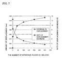
- a sample of piezoelectric element having the characteristics described above was caused to undergo a durability test in which a predetermined drive pulse is continuously applied to the sample thirty billion times.
- Fig. 7 shows the result of examining the amount of displacement of the piezoelectric element and a decrease in the displacement.
- a piezoelectric layer had a thickness of 1.5 ⁇ m
- a lower electrode film had a thickness of 200 nm
- an upper electrode film had a thickness of 50 nm.
- the drive pulse applied in the durability test was a sin wave of a voltage of 50V and a frequency of 100kHz.
- a drive pulse applied during displacement measurement was a trapezoidal wave of a voltage of 30V and a frequency of 800Hz.
- the amount of displacement thereof was decreased along with the increase in the number of withstand pulses, that is, the rate of displacement decrease was increased.
- the rate of displacement decrease was as significantly low as 13.3%.
- the piezoelectric layer is formed by use of the sol-gel method or the MOD method. However, it is not particularly limited to this.
- the piezoelectric layer may be formed by means of a sputtering method. In a case of forming the piezoelectric film by means of the sputtering method as described, it suffices that post annealing is performed on the piezoelectric precursor film for half an hour to three hours at 650 to 750°C.
- At least any one dopant selected from nickel (Ni), manganese (Mn) and strontium (Sr) was doped to each of the piezoelectric layers 70 constituting the piezoelectric element 300.
- Ni nickel
- Mn manganese
- Sr strontium
- the inkjet recording head according to each of those embodiments constitutes a part of a recording head unit provided with an ink passage communicating with an ink cartridge and the like, and is installed in an inkjet recording device.
- Fig. 8 is a schematic configuration diagram showing an example of the inkjet recording device.
- recording head units 1A and 1B including the respective inkjet recording heads are detachably provided to cartridges 2A and 2B constituting ink supply means.
- a carriage 3 on which the recording head units 1A and 1B are mounted is provided to a carriage shaft 5 fixed to the device main body 4 in a way that the carriage 3 can be freely moved in the direction in which the shaft extends.
- These recording head units 1A and 1B are assigned to ejecting black ink compositions and color ink compositions respectively.
- a drive power from a drive motor 6 is transmitted to the carriage 3 though a plurality of gears, which are not illustrated, and a timing belt 7.
- the carriage 3 on which the recording head units 1A and 1B are mounted is caused to move along the carriage shaft 5.
- the device main body 4 is provided with a platen 8 along the carriage shaft 5.
- a recording sheet S which is a recording medium such as a sheet of paper, and which has been fed by feed rollers and the like, is designed to be transferred on the platen 8, the feed rollers being not illustrated.
- liquid-jet head which ejects a liquid other than ink
- examples of liquid-jet head which eject a liquid other than ink includes various recording heads used for image recording devices such as printers; color-material-jet heads used for manufacturing color filters of liquid crystal display devices and the like; electrode-material-jet heads used for forming electrodes of organic EL display devices, FED (Field Emission Display) devices and the like; bio-organic-substance-jet heads used for manufacturing bio-chips; and the like.
Landscapes
- Engineering & Computer Science (AREA)
- Manufacturing & Machinery (AREA)
- Chemical & Material Sciences (AREA)
- Dispersion Chemistry (AREA)
- Aviation & Aerospace Engineering (AREA)
- Health & Medical Sciences (AREA)
- Life Sciences & Earth Sciences (AREA)
- Hydrology & Water Resources (AREA)
- Public Health (AREA)
- Water Supply & Treatment (AREA)
- Particle Formation And Scattering Control In Inkjet Printers (AREA)
- General Electrical Machinery Utilizing Piezoelectricity, Electrostriction Or Magnetostriction (AREA)
Applications Claiming Priority (2)
| Application Number | Priority Date | Filing Date | Title |
|---|---|---|---|
| JP2005081729 | 2005-03-22 | ||
| JP2005356706A JP2006303425A (ja) | 2005-03-22 | 2005-12-09 | 圧電素子及び液体噴射ヘッド並びに液体噴射装置 |
Publications (2)
| Publication Number | Publication Date |
|---|---|
| EP1705723A2 true EP1705723A2 (de) | 2006-09-27 |
| EP1705723A3 EP1705723A3 (de) | 2006-10-04 |
Family
ID=36602389
Family Applications (1)
| Application Number | Title | Priority Date | Filing Date |
|---|---|---|---|
| EP20060005623 Withdrawn EP1705723A3 (de) | 2005-03-22 | 2006-03-20 | Piezoelektrisches Element, Flüssigkeitsstrahlkopf und Flüssigkeitsstrahlvorrichtung |
Country Status (4)
| Country | Link |
|---|---|
| US (1) | US7498724B2 (de) |
| EP (1) | EP1705723A3 (de) |
| JP (1) | JP2006303425A (de) |
| KR (1) | KR20060102520A (de) |
Families Citing this family (4)
| Publication number | Priority date | Publication date | Assignee | Title |
|---|---|---|---|---|
| JP5170356B2 (ja) * | 2005-03-22 | 2013-03-27 | セイコーエプソン株式会社 | 圧電素子及び液体噴射ヘッド並びに液体噴射装置 |
| JP5592104B2 (ja) | 2009-02-17 | 2014-09-17 | 富士フイルム株式会社 | 圧電体膜並びにそれを備えた圧電素子及び液体吐出装置 |
| JP5585209B2 (ja) * | 2009-05-28 | 2014-09-10 | 株式会社リコー | 電気機械変換素子の製造方法、該製造方法により製造した電気機械変換素子、液滴吐出ヘッド及び液滴吐出装置 |
| EP3196952B1 (de) * | 2016-01-21 | 2019-06-19 | AT & S Austria Technologie & Systemtechnik Aktiengesellschaft | Piezoelektrischer mems-wandler, der an einer leiterplattentragstruktur ausgebildet ist |
Citations (4)
| Publication number | Priority date | Publication date | Assignee | Title |
|---|---|---|---|---|
| GB509838A (en) * | 1938-01-21 | 1939-07-21 | Ass Equipment Co Ltd | Improvements in or relating to liquid-fuel injection internal-combustion engines |
| US3110626A (en) * | 1961-08-17 | 1963-11-12 | Minnesota Mining & Mfg | Apparatus for coating discrete solid material |
| US3496323A (en) * | 1965-12-20 | 1970-02-17 | Air Reduction | Gas shielded arc welding of steel |
| JP2004107181A (ja) | 2002-09-20 | 2004-04-08 | Canon Inc | 圧電体素子形成用組成物、圧電体膜の製造方法、圧電体素子及びインクジェット記録ヘッド |
Family Cites Families (27)
| Publication number | Priority date | Publication date | Assignee | Title |
|---|---|---|---|---|
| US4397886A (en) | 1981-05-06 | 1983-08-09 | Sprague Electric Company | Method for making a ceramic intergranular barrier-layer capacitor |
| US5112433A (en) | 1988-12-09 | 1992-05-12 | Battelle Memorial Institute | Process for producing sub-micron ceramic powders of perovskite compounds with controlled stoichiometry and particle size |
| US5219811A (en) | 1989-08-31 | 1993-06-15 | Central Glass Company, Limited | Powder composition for sintering into modified barium titanate semiconductive ceramic |
| GB9025706D0 (en) | 1990-11-27 | 1991-01-09 | Xaar Ltd | Laminate for use in manufacture of ink drop printheads |
| JP3327149B2 (ja) | 1995-12-20 | 2002-09-24 | セイコーエプソン株式会社 | 圧電体薄膜素子及びこれを用いたインクジェット式記録ヘッド |
| US5969935A (en) | 1996-03-15 | 1999-10-19 | Ramtron International Corporation | Use of calcium and strontium dopants to improve retention performance in a PZT ferroelectric film |
| US6398349B1 (en) * | 1998-03-04 | 2002-06-04 | Seiko Epson Corporation | Piezoelectric device, ink-jet printing head, and method for manufacturing same, and printer |
| US6203608B1 (en) | 1998-04-15 | 2001-03-20 | Ramtron International Corporation | Ferroelectric thin films and solutions: compositions |
| JP2000173301A (ja) * | 1998-12-10 | 2000-06-23 | Seiko Epson Corp | 圧電発光素子、表示装置およびそれらの製造方法 |
| JP3671791B2 (ja) | 1999-02-08 | 2005-07-13 | 株式会社村田製作所 | 圧電磁器組成物およびそれを用いた圧電セラミック素子 |
| JP2001113705A (ja) | 1999-10-19 | 2001-04-24 | Casio Comput Co Ltd | ドライエッチング用金属マスク、これを備えたインクジェットプリンタヘッド及びその製造方法 |
| JP3202012B1 (ja) | 2000-03-29 | 2001-08-27 | 松下電器産業株式会社 | 圧電アクチュエータ、インクジェットヘッド及びインクジェット式記録装置 |
| JP2001302349A (ja) | 2000-04-19 | 2001-10-31 | Tokin Corp | 圧電磁器組成物 |
| JP2001302345A (ja) | 2000-04-19 | 2001-10-31 | Nitsukatoo:Kk | 耐久性にすぐれたジルコニア質焼結体およびその製造方法 |
| JP2001302348A (ja) | 2000-04-19 | 2001-10-31 | Tokin Corp | 圧電磁器組成物 |
| JP2001302350A (ja) | 2000-04-19 | 2001-10-31 | Tokin Corp | 圧電磁器組成物 |
| JP2002226266A (ja) | 2001-01-30 | 2002-08-14 | Nec Tokin Corp | 圧電磁器組成物 |
| EP1367658B1 (de) | 2001-12-18 | 2016-04-13 | Panasonic Intellectual Property Management Co., Ltd. | "piezoelektrisches element, tintenstrahlkopf, winkelgeschwindigkeitssensor, herstellungsverfahren dafür und aufzeichnungsvorrichtung des tintenstrahltyps" |
| KR100480501B1 (ko) * | 2002-06-19 | 2005-04-06 | 학교법인 포항공과대학교 | 유기금속 화학증착법에 의한 pzt 박막의 제조방법 |
| TWI230477B (en) * | 2002-09-20 | 2005-04-01 | Canon Kk | Composition for forming piezoelectric film, producing method for piezoelectric film, piezoelectric element and ink jet recording head |
| JP3971279B2 (ja) * | 2002-09-20 | 2007-09-05 | キヤノン株式会社 | 圧電体素子の製造方法 |
| JP2004235553A (ja) | 2003-01-31 | 2004-08-19 | Canon Inc | 圧電体膜成膜用支持基板、圧電体素子、インクジェット記録ヘッド |
| JP2005082424A (ja) | 2003-09-05 | 2005-03-31 | Nec Tokin Corp | 圧電磁器組成物 |
| US7132057B2 (en) | 2003-10-15 | 2006-11-07 | Piezotech, Llc | Compositions for high power piezoelectric ceramics |
| KR100865798B1 (ko) * | 2004-02-27 | 2008-10-28 | 캐논 가부시끼가이샤 | 압전 박막, 압전 박막의 제조방법, 압전 소자, 및 잉크제트 기록 헤드 |
| US20050199924A1 (en) * | 2004-03-10 | 2005-09-15 | Fox Glen R. | Optimized ferroelectric material crystallographic texture for enhanced high density feram |
| JP2006160582A (ja) * | 2004-12-10 | 2006-06-22 | Taiheiyo Cement Corp | 圧電セラミックス用焼結助剤および圧電セラミックス |
-
2005
- 2005-12-09 JP JP2005356706A patent/JP2006303425A/ja active Pending
-
2006
- 2006-03-20 EP EP20060005623 patent/EP1705723A3/de not_active Withdrawn
- 2006-03-21 US US11/384,315 patent/US7498724B2/en not_active Expired - Lifetime
- 2006-03-22 KR KR20060026068A patent/KR20060102520A/ko not_active Ceased
Patent Citations (4)
| Publication number | Priority date | Publication date | Assignee | Title |
|---|---|---|---|---|
| GB509838A (en) * | 1938-01-21 | 1939-07-21 | Ass Equipment Co Ltd | Improvements in or relating to liquid-fuel injection internal-combustion engines |
| US3110626A (en) * | 1961-08-17 | 1963-11-12 | Minnesota Mining & Mfg | Apparatus for coating discrete solid material |
| US3496323A (en) * | 1965-12-20 | 1970-02-17 | Air Reduction | Gas shielded arc welding of steel |
| JP2004107181A (ja) | 2002-09-20 | 2004-04-08 | Canon Inc | 圧電体素子形成用組成物、圧電体膜の製造方法、圧電体素子及びインクジェット記録ヘッド |
Also Published As
| Publication number | Publication date |
|---|---|
| KR20060102520A (ko) | 2006-09-27 |
| US7498724B2 (en) | 2009-03-03 |
| US20060244788A1 (en) | 2006-11-02 |
| JP2006303425A (ja) | 2006-11-02 |
| EP1705723A3 (de) | 2006-10-04 |
Similar Documents
| Publication | Publication Date | Title |
|---|---|---|
| US7520038B2 (en) | Piezoelectric element, method of manufacturing the same, liquid-jet head, method of manufacturing the same, and liquid-jet apparatus | |
| EP1911590B1 (de) | Aktuatorvorrichtung, Flüssigkeitsstrahlkopf und Verfahren zur Herstellung der Aktuatorvorrichtung | |
| EP1707368B1 (de) | Piezoelektrisches Element, Flüssigkeitstrahlkopf und -gerät | |
| US7479728B2 (en) | Piezoelectric element, method of manufacturing the same, liquid-jet head, method of manufacturing the same, and liquid-jet apparatus | |
| CN101638004B (zh) | 液体喷射头和液体喷射装置及压电元件 | |
| EP1707366B1 (de) | Piezoelektrisches Element, Aktuatorvorrichtung, Flüssigkeitsstrahlkopf und -vorrichtung | |
| US8079677B2 (en) | Liquid ejecting head, liquid ejecting apparatus, and piezoelectric actuator | |
| US20060132549A1 (en) | Method for producing actuator device, and liquid-jet apparatus | |
| EP1707367B1 (de) | Piezoelektrisches Element, Aktuatorvorrichtung, Flüssigkeitsstrahlkopf und -vorrichtung | |
| US7498724B2 (en) | Piezoelectric element, liquid-jet head and liquid-jet apparatus | |
| US7514854B2 (en) | Piezoelectric element, liquid-jet head using piezoelectric element and liquid-jet apparatus | |
| JP2007073931A (ja) | アクチュエータ装置の製造方法及びアクチュエータ装置並びに液体噴射ヘッド及び液体噴射装置 | |
| JP2009049433A (ja) | 圧電素子及びその製造方法、液体噴射ヘッド及びその製造方法並びに液体噴射装置 | |
| JP2009226728A (ja) | 液体噴射ヘッドの製造方法及び圧電素子の製造方法 | |
| JP2011230427A (ja) | 液体噴射ヘッド及び液体噴射装置 | |
| JP2006245248A (ja) | 圧電素子及びその製造方法、液体噴射ヘッド及びその製造方法並びに液体噴射装置 |
Legal Events
| Date | Code | Title | Description |
|---|---|---|---|
| PUAI | Public reference made under article 153(3) epc to a published international application that has entered the european phase |
Free format text: ORIGINAL CODE: 0009012 |
|
| PUAL | Search report despatched |
Free format text: ORIGINAL CODE: 0009013 |
|
| AK | Designated contracting states |
Kind code of ref document: A2 Designated state(s): AT BE BG CH CY CZ DE DK EE ES FI FR GB GR HU IE IS IT LI LT LU LV MC NL PL PT RO SE SI SK TR |
|
| AX | Request for extension of the european patent |
Extension state: AL BA HR MK YU |
|
| AK | Designated contracting states |
Kind code of ref document: A3 Designated state(s): AT BE BG CH CY CZ DE DK EE ES FI FR GB GR HU IE IS IT LI LT LU LV MC NL PL PT RO SE SI SK TR |
|
| AX | Request for extension of the european patent |
Extension state: AL BA HR MK YU |
|
| 17P | Request for examination filed |
Effective date: 20070326 |
|
| AKX | Designation fees paid |
Designated state(s): DE FR GB |
|
| 17Q | First examination report despatched |
Effective date: 20071220 |
|
| STAA | Information on the status of an ep patent application or granted ep patent |
Free format text: STATUS: THE APPLICATION IS DEEMED TO BE WITHDRAWN |
|
| 18D | Application deemed to be withdrawn |
Effective date: 20090331 |