EP1703396B1 - Fehlererkennung und -korrektur - Google Patents
Fehlererkennung und -korrektur Download PDFInfo
- Publication number
- EP1703396B1 EP1703396B1 EP05253847.7A EP05253847A EP1703396B1 EP 1703396 B1 EP1703396 B1 EP 1703396B1 EP 05253847 A EP05253847 A EP 05253847A EP 1703396 B1 EP1703396 B1 EP 1703396B1
- Authority
- EP
- European Patent Office
- Prior art keywords
- data
- error
- correction
- error detection
- processing apparatuses
- Prior art date
- Legal status (The legal status is an assumption and is not a legal conclusion. Google has not performed a legal analysis and makes no representation as to the accuracy of the status listed.)
- Expired - Lifetime
Links
Images









Classifications
-
- G—PHYSICS
- G06—COMPUTING OR CALCULATING; COUNTING
- G06F—ELECTRIC DIGITAL DATA PROCESSING
- G06F11/00—Error detection; Error correction; Monitoring
-
- G—PHYSICS
- G06—COMPUTING OR CALCULATING; COUNTING
- G06F—ELECTRIC DIGITAL DATA PROCESSING
- G06F11/00—Error detection; Error correction; Monitoring
- G06F11/07—Responding to the occurrence of a fault, e.g. fault tolerance
- G06F11/08—Error detection or correction by redundancy in data representation, e.g. by using checking codes
- G06F11/10—Adding special bits or symbols to the coded information, e.g. parity check, casting out 9's or 11's
- G06F11/1008—Adding special bits or symbols to the coded information, e.g. parity check, casting out 9's or 11's in individual solid state devices
- G06F11/1044—Adding special bits or symbols to the coded information, e.g. parity check, casting out 9's or 11's in individual solid state devices with specific ECC/EDC distribution
-
- G—PHYSICS
- G06—COMPUTING OR CALCULATING; COUNTING
- G06F—ELECTRIC DIGITAL DATA PROCESSING
- G06F11/00—Error detection; Error correction; Monitoring
- G06F11/07—Responding to the occurrence of a fault, e.g. fault tolerance
- G06F11/14—Error detection or correction of the data by redundancy in operations
Definitions
- the present invention relates to a control method for error detection & correction apparatus, an error detection & correction apparatus, an information processing system, a control program for error detection & correction apparatus, a data processing apparatus, and in particular a technique effectively applicable to a detection and correction of data error, et cetera, by using an error correcting code (ECC) in a data transmission or accumulation.
- ECC error correcting code
- known is a method of using an ECC for detecting and correcting a data error which occurs in a bus as information transmission path or memory storing information.
- error check unit In the case of letting one ECC processing apparatus process a unit of error check ("error check unit” hereinafter unless otherwise noted) in an ECC application, it is necessary to increase the number of pins in the ECC processing apparatus according to a data size of the error check unit, or transmit data by folding itself.
- a countermeasure is conceivable to have a plurality of ECC processing apparatuses share the error check unit, in which a method is adopted such that each ECC processing apparatus sharing the processing of the error check unit performs a partial error check and a processing apparatus in upper echelon (e.g., a controller or CPU in upper echelon) achieves a final error check and correction of the error check unit.
- a method is known to exchange a partial syndrome between a plurality of ECC processing apparatuses sharing an error check unit and generate a true syndrome of the error check unit, as disclosed by the patent documents 1 or 2 listed below.
- an error check & correction circuit comprising means for outputting a partial syndrome to the outside by generating it based on a part of a codeword being inputted from the outside, means for generating a syndrome of a codeword based on the partial syndrome inputted from the outside and partial syndrome generated in the inside, and means for correcting a partial error of a codeword by decoding the generated syndrome.
- the patent document 2 has disclosed a technique to enable a plurality of ECC circuits with the exact same configuration to share-process a multi-bit data by making the ECC circuits sharing each of a plurality of blocks adaptable to either of an upper bit block or lower bit block by an external control signal only, in the case of generating an ECC for each of a plurality of blocks which are obtained by dividing a multi-bit data into plural parts.
- each ECC processing apparatus sharing the error check unit will no longer be able to handle a high level data processing (e.g., a data processing only possible following an error check such as a partial merge of data) .
- a high level data processing e.g., a data processing only possible following an error check such as a partial merge of data
- US 5, 841, 795 A discloses a method of detecting and correcting errors in a memory subsystem of a computer.
- the method includes beginning a write operation of N data bits to a memory, generating M check bits from the N data bits, writing the N data bits and the M check bits to the memory, reading the N data bits and M check bits from the memory, generating X syndrome bits from the N data bits and the M check bits, and using the X syndrome bits to detect and correct errors.
- a purpose of the present invention is to enable each processing apparatus to perform a high level data processing such as requiring a merge processing of data in an error detection & correction technique for processing data by the unit of ECC error check in a plurality of partaking processing apparatuses.
- Another purpose of the present invention is to enable each processing apparatus to perform a diverse error detection & correction processing corresponding to a category of detected error, et cetera, in an error detection & correction technique for processing data by the unit of ECC error check in a plurality of partaking processing apparatuses.
- Yet another purpose of the present invention is to accomplish an error detection & correction capability equivalent to the case in which one data processing apparatus processes data by the unit of ECC error check.
- the invention proposes a control method according to claim 1 and an error detection & correction apparatus according to claim 8. Further advantageous embodiments of the invention are disclosed in the dependent claims.
- a control method for an error detection & correction apparatus comprising a plurality of data processing apparatuses which reside in a data communication path and partake in exchanging data by the unit of error correcting code, and a plurality of information exchange paths which are installed between the plurality of data processing apparatuses; and generating a true syndrome by exchanging a partial syndrome relating to a part of the data partaken by each of the data processing apparatuses by way of the information exchange paths, comprising the step of exchanging renewal information relating to a part of the data partaken by each of the data processing apparatuses with the other data processing apparatus by way of the information exchange path.
- an error detection & correction apparatus comprising a plurality of data processing apparatuses which reside in a data communication path and partake in exchanging data by the unit of error correcting code and a plurality of information exchange paths which are installed between the plurality of data processing apparatuses; and generating a true syndrome by exchanging a partial syndrome relating to a part of the data partaken by each of the data processing apparatuses by way of the information exchange paths, comprising: an information exchange unit for exchanging renewal information relating to a part of the data partaken by each of the data processing apparatuses with the other data processing apparatus by way of the information exchange path.
- an information processing system including a storage apparatus, an access apparatus for accessing the storage apparatus, a data transmission path for connecting the storage apparatus with the access apparatus and an error detection & correction apparatus residing in the data transmission path, wherein the error detection & correction apparatus comprises a plurality of data processing apparatuses partaking in exchanging data by the unit of error correcting code in data transmission paths, information exchange paths installed between a plurality of the data processing apparatuses, and an information exchange unit for exchanging a partial syndrome relating to a part of the data partaken by each of the data processing apparatuses and renewal information relating to a part of the data partaken by each of the data processing apparatus with a plurality of the data processing apparatuses by way of the information exchange paths.
- a signal for carrying control program for an error detection & correction apparatus comprising a plurality of data processing apparatuses which reside in a data communication path and partake in exchanging data by the unit of error correcting code, and a plurality of information exchange paths which are installed between the plurality of data processing apparatuses, wherein the signal for carrying control program makes each of the data processing apparatuses carry out the process of exchanging a partial syndrome relating to a part of the data partaken by each of the data processing apparatuses and renewal information relating to a part of the data partaken by each of the data processing apparatus with a plurality of the data processing apparatuses by way of the information exchange paths.
- a data processing apparatus being included in an error detection & correction apparatus residing in a data communication path and partaking in exchanging data by the unit of error correcting code, comprising an information exchange unit for exchanging a partial syndrome relating to a part of the data partaken by the own apparatus and renewal information relating to a part of the data partaken by own apparatus with other data processing apparatus.
- each of data processing apparatuses is enabled for a high level data processing such as a partial data merge by exchanging error correction information between a plurality of data processing apparatuses instead of being limited by a partial syndrome, in an error detection & correction technique for processing data by the unit of ECC error check ("ECC error check unit” hereinafter unless otherwise noted) in a plurality of partaking processing apparatuses.
- ECC error check unit the unit of ECC error check
- a high level data processing such as a read modify write (i.e., a partial data merge) is enabled even if data by the ECC error check unit is processed across a plurality of data processing apparatuses, each of which is configured to deal with data protected by the ECC, such as a memory controller.
- a read modify write i.e., a partial data merge
- a diverse error detection and correction processing in response to a detected error are enabled by exchanging error correction information other than partial syndromes between a plurality of data processing apparatuses. Furthermore, an error detection & correction capability equivalent to the case of a single data processing apparatus dealing with data by an error check unit can be achieved.
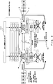
- Fig. 1 is a conceptual diagram showing an example operation of error detection & correction apparatus according to an embodiment of the present invention
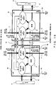
- Fig. 2 is a conceptual diagram showing a modified operation of error detection & correction apparatus according to an embodiment of the present invention.
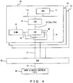
- Fig. 3 is a block diagram showing an example comprisal of data processing apparatus constituting a memory access control apparatus as an example of error detection & correction apparatus according to an embodiment of the present invention
- Fig. 4 is a conceptual diagram showing an example comprisal of information processing system according to an embodiment of the present invention.
- the information processing system according to the present embodiment comprises a plurality of information processing apparatuses 10, a bus switch 20 (i.e., GDX) and one or a plurality of input & output equipments 30 (i.e., FLI) .
- a bus switch 20 i.e., GDX
- input & output equipments 30 i.e., FLI
- the bus switch 20 switches connections of information transmission paths between these information processing apparatuses 10 and input & output equipment 30.
- the each of information processing apparatuses 10 includes a CPU 11, a system bus 11a, an input & output control apparatus 12 (i.e., FLN), a memory apparatus 13 (i.e., DIMM), a memory access control apparatus 14 (i.e., error detection & correction apparatus) (LDX), an upper side bus 15, a memory bus 16 and a lower side bus 17.
- a CPU 11 a system bus 11a
- an input & output control apparatus 12 i.e., FLN
- a memory apparatus 13 i.e., DIMM
- a memory access control apparatus 14 i.e., error detection & correction apparatus
- the CPU 11 executes an information processing by accessing to a program and data stored in the memory apparatus 13.
- the input & output control apparatus 12 controls information exchanges between the CPU 11 and the memory apparatus 13, other information processing apparatuses 10 and input & output equipment 30.
- the memory apparatus 13 stores a program and data executed by the CPU 11.
- the memory access control apparatus 14 functions as an error detection & correction apparatus in the case of the present embodiment. That is, the memory access control apparatus 14 performs an error detection & correction by using an ECC for data read / written, out of / in, the memory apparatus 13 by way of the memory bus 16, upper side bus 15 and lower side bus 17.
- Each of the memory access control apparatus 14 is constituted by a plurality of data processing apparatuses 40 (LDX), each of which comprises as exemplified by Fig. 3 .
- LDX data processing apparatuses 40
- each data processing apparatus 40 comprises a memory access control logic 41, a write buffer 42 (WRQ), a read buffer 43 (RDQ) and an information exchange buffer 44 (ECC).
- WRQ write buffer 42
- RDQ read buffer 43
- ECC information exchange buffer 44
- a plurality of the data processing apparatuses 40 are interconnected by an information exchange bus 50 (i.e., information exchange path).
- the write buffer 42 temporarily stores write data to be written in the memory apparatus 13 from the CPU 11, other information processing apparatus 10, input & output equipment 30, et cetera.
- the read buffer 43 temporarily stores read data which is read out of the memory apparatus 13.
- the memory access control logic 41 comprises a control logic (i.e., control program) in the form of software, firmware or hardware for accomplishing the functions as described below.
- control logic i.e., control program
- the memory access control logic 41 comprises the function of performing an ECC processing for a read or write data in a data width of the upper side bus 15 and lower side bus 17 by sharing with other partaking data processing apparatus 40 by exchanging a series of information therewith by way of the information exchange bus 50.
- the memory access control logic 41 comprises the function of enabling a conversion and error check & correction of a check bit also at the time of partially renewing data by the ECC error check unit for the upper side bus 15, memory bus 16 and lower side bus 17.
- the memory access control logic 41 comprises the function of selecting an operation for using, or not using, the information exchange bus 50 for data by the unit of ECC error check in response to a pattern of partial renewal information.
- the memory access control logic 41 comprises the function of altering a check bit (i.e., renewing) which regards all the data partaken by the other data processing apparatuses 40 as zero (0) for the data after being partially renewed, not for the partial renewal information at the time of error correction, and of exchanging with the other data processing apparatus 40 by way of the information exchange bus 50.
- a check bit i.e., renewing
- the memory access control logic 41 comprises the function of exchanging detected information of a specific error pattern which has been detected within its own apparatus with the other data processing apparatus 40 by way of the information exchange bus 50, and changing an error correction operation.
- the memory access control logic 41 comprises the function of preventing an erroneous correction due to a use of a wrong partial syndrome through the steps of adding a synchronism confirmation signal to a partial syndrome, and an ECC protection to the information exchange bus 50 per se as well; exchanging with the other data processing apparatus 40 by way of the aforementioned information exchange bus 50; and detecting an erroneous usage timing of the partial syndrome in own apparatus and the other data processing apparatuses 40.
- the memory access control logic 41 comprises the function of controlling a data length variably of a partial syndrome being exchanged with other data processing apparatus 40 by way of the information exchange bus 50.
- the memory access control logic 41 comprises the function of not only sending corrected data by exchanging a partial syndrome by way of the information exchange bus 50 out to the input & output control apparatus 12, et cetera, but also sending out pre-correction data in advance followed by notifying of a detected error afterwards.
- An example practice is to divide a 128-byte data into four of LDX / DIMM and make the best use of the upper side bus 15 and/or lower side bus 17 between FLN - LDX and/or FLN - GDX in order to minimize a transmission latency of a 128-byte cache line in the CPU 11. Consequently, as a 16-byte ECC straddles two LDXes, do not basically perform an error check and instead let the LDX transmit the data, S4EC - D4ED (Single 4-bit block Error Correction / Double 4-bit block Error Detection) -code, as is, to the devices such as FLN and FLI.
- S4EC - D4ED Single 4-bit block Error Correction / Double 4-bit block Error Detection
- Fig. 5 shows a bus as a subject of protection by an ECC (16-byte S4EC - D4ED) by a 32 SMP (symmetrical multi processor) basic comprisal.
- the FLN i.e., input & output control apparatus 12
- FLI i.e., input & output equipment 30
- the LDX also performs the check & correction in order to complete an identification of error spot, a later described patrol in the DIMM (i.e., memory apparatus 13) and a data moving at the time of partial write such as a read modify write, all within the LDX.
- the information exchange bus 50 comprises two kinds of buses, i.e., bus #0 and bus #1, whose data transmission directions are mutually the opposite.
- the next description is about an error control by the memory access control logic 41 performed by each of the data processing apparatuses 40 (i.e., LDX) constituting the memory access control apparatus 14.
- the memory access control apparatus 14 comprising a plurality of LDXes performs the operations of a memory read, memory write, partial write (i.e., read modify write) and patrol (i.e., periodical operation monitor processing), all for accessing to the memory apparatus 13.
- an exchange of syndrome is performed by using the information exchange bus 50 which will also be used for a data transmission path at the time of a degenerate operation.
- a transmission protocol for the information exchange bus 50 will be described later.
- the plurality of data processing apparatuses 40 i.e., LDXes #0 / #1
- partaking in a data width of the ECC error check unit e.g., 16 bytes
- transmit a partial syndrome detected within own apparatus to the other partaking apparatus by way of the information exchange bus 50. That is, to generate a syndrome to send out to the other apparatus by setting zero (0) as the value for the other 8 bytes of data partaken by the other LDX. If there is no error in the data, the values of mutually sent syndromes are the same.
- the memory access control logic 41 comprised by the LDX reports the error to an FLN in an upper echelon through a reply bus 15b.
- An error is classified into three types (i.e., SBE: single block error (correctable), DBE: double block error (uncorrectable) and detection of poisoned data) for each of the four memory operations (i.e., memory read, memory write, partial write and patrol) in the error report.
- SBE single block error
- DBE double block error
- detection of poisoned data i.e., memory read, memory write, partial write and patrol
- LDXes #0 and #1, or LDXes #2 and #3, in the example shown by Fig. 5 the members of a team of LDXes (LDXes #0 and #1, or LDXes #2 and #3, in the example shown by Fig. 5 ) straddled by an ECC check unit report the same content, except for a memory write at a degenerate operation, et cetera, in which only one LDX in a team may report.
- Fig. 7A is a conceptual diagram showing an example comprisal of the information exchange bus 50 according to the present embodiment.
- the information exchange bus 50 comprises the bus #0 and bus #1, with each thereof comprising respective signals by the bit widths (i.e., the numbers of pins) as exemplified by Fig. 7B .
- the transmitted data is protected by the 21-bit data ECC (i.e., SEC - DED) in either the bus #0 or bus #1 constituting the information exchange bus 50.
- ECC 21-bit data ECC
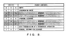
- Fig. 8 describes an example setup of identifier information about information packet exchanged between LDXes by way of the information exchange bus 50.
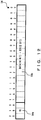
- Figs. 9 , 10 , 11 and 12 are conceptual diagrams exemplifying respective formats of various packets.
- Fig. 9 shows an example configuration of syndrome exchange packet 51 for exchanging a syndrome.
- the syndrome exchange packet 51 comprises an ID part 51a, a reserve part 51b, error identifier information 51c and a syndrome value 51d.
- the ID part 51a is set with "100" corresponding to a "syndrome exchange” shown by Fig. 8 .
- the error identifier information 51c is set with an information bit for identifying a poisoned data or otherwise.
- a configuration may be such that, if the error identifier information 51c is set, the syndrome value 51d stores information for indicating an error category instead of a syndrome value so as to exchange between the corresponding LDXes and switch the error correction operation in the respective LDXes.
- Fig. 10 shows an example configuration of renewal information exchange packet 52 for exchanging renewal information.
- the renewal information exchange packet 52 comprises an ID part 52a, a reserve part 52b, an operation change flag 52c and renewal information 52d.
- the ID part 52a is set with "101" corresponding to a "renewal information exchange” shown by Fig. 8 .
- the renewal information 52d stores a post-correction data obtained by the LDX which has transmitted the aforementioned renewal information exchange packet 52.
- the operation change flag 52c is used for changing an operation if a specific error pattern is detected as a result of the LDXes notifying each other of detecting the aforementioned specific error pattern.
- Fig. 11 shows an example configuration of synchronism check packet 53 for a synchronism check.
- the synchronism check packet 53 comprises an ID part 53a and synchronism identifier information 53b.
- the ID part 53a is set with "001" corresponding to a "synchronism check" shown by Fig. 8 .
- the synchronism identifier information 53b is set with a Sync-ID for controlling a synchronism between the LDXes.
- a synchronism check is for controlling a synchronism between the LDXes #0 and #1, and between the LDXes #2 and #3, mutually partaking in the ECC data unit, not checking the synchronism among all the LDXes.
- Fig. 12 shows an example configuration of data packet 54 at the time of a degenerate operation ("at-degenerate operation data packet 54" hereinafter) .
- the at-degenerate operation data packet 54 comprises an ID part 54a and transmission data 54b.
- the ID part 54a is set with "111" corresponding to a "degenerate operation data transmission” shown by Fig. 8 .
- the transmission data 54b stores transmission data at a degenerate operation.
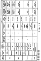
- Fig. 13 describes a list of error check control by each LDX, showing the error check operation in the operations of a read, write, p-write (i.e., partial write) and patrol.
- Fig. 14 shows a read operation by the memory apparatus 13 (i.e., DIMM) at the normal operation.
- the memory access control logic 41 participate in executing an ECC check for readout data by transmitting the read data out of the memory apparatus 13 to the input & output control apparatus 12 and exchanging the partial syndrome values by way of the information exchange bus 50.
- the transmission of the data to the input & output control apparatus 12 is put in a higher priority and an error will be reported thereto later by using the reply bus 15b if the error is detected in the readout data.
- a data read from the memory apparatus 13 to the input & output equipment 30 will likewise be done.
- the memory access control logic 41 performs a Scrub Write demand to the input & output control apparatus 12 by way of the replybus 15b and executes a Scrub Write, which repairs stored data within the memory apparatus 13, for a storage zone of an address instructed by the input & output control apparatus 12 by way of the address bus 15a.
- Fig. 15 shows an operation of the LDX in a write operation for the memory apparatus 13.
- a plurality of LDXes partake in executing an ECC check and correction for the write data coming in from the input & output control apparatus 12 by way of the upper side bus 15, and, if an error is detected, the memory access control logic 41 comprised in the inside of each LDX corrects the error to write in the memory apparatus 13 and also reports the error to the input & output control apparatus 12 by way of the reply bus 15b.
- a data write processing for the data from the input & output equipment 30 to the memory apparatus 13 will likewise be done.
- Fig. 16 shows an operation of the LDX in a partial write (i.e., read modify write) for the memory apparatus 13.
- each LDX Having received a write data from an FLN or GDX, each LDX performs an ECC check and correction by mutually exchanging syndromes, and reports an error to the FLN by way of the reply bus 15b if the error is detected.
- each LDX also performs an ECC check and correction by mutually exchanging syndromes, and report an error to the FLN by way of the reply bus 15b if the error is detected.
- each LDX mutually exchanges correction results relating to the write and read data as the renewal information by way of the information exchange bus 50.
- the LDX merges the write data processed through the ECC check & correction and the read data out of the DIMM by including the ECC check bit to write in the DIMM. If a DBE (double block error) or a Poisoned Data is detected as a result of the ECC check, the Poisoned Data will be written in the DIMM.
- the present embodiment lets the two LDXes partaking in the ECC check & correction exchange with each other the renewal information for the own apparatuses reflected by the correction result of the read data and that of the write data, in addition to two syndromes relating to the read and write data by way of the information exchange bus 50.
- the exchange of the renewal information uses the above described renewal information exchange packet 52.
- Fig. 17 shows an operation of the LDX in the patrol. After reading data out of the DIMM, each LDX performs an ECC check by exchanging syndromes by way of the information exchange bus 50 and reports an error to the FLN by way of the reply bus 15b if the error is detected.
- the LDX demands a Scrub Write to the FLN to correct the error in the DIMM.
- the two data processing apparatuses 40 partaking in an ECC check simultaneously receive a write data through the data communication path (i.e., upper side bus 15 or lower side bus 17).
- the LDX (#0) and LDX (#1) send partial syndromes SD-A0 and SD-B0, respectively, to each other, generate a true syndrome SD-AB0 and perform an error correction. Likewise they further perform an error correction operation.
- the sequence of write and read operations is not important.
- the LDXes #0 and #1 transmit renewal information (i.e., a changed part by the error correction operation) to each other, merge the data and reconstruct a check bit.
- each LDX can change an operation at an ECC error detection when detecting a specific error pattern by using the above described operation change flag 52c of the renewal information exchange packet 52, which will be described in reference to Fig. 2 .
- the description associated with Fig. 2 is about a pair of LDXes (#0) and (#1).
- Fig. 2 exemplifies the case of suppressing an error correction operation, if detecting a specific error pattern, by the LDXes exchanging the aforementioned specific error pattern with each other by way of the information exchange bus 50 with a use of the operation change flag 52c of the renewal information exchange packet 52 ( Fig. 10 ).
- the renewal information 52d stores the specific error pattern causing the error.
- Such control operation performed by the LDX is quite useful in an information processing system adopting the method of identifying an error occurrence point or controlling a program flow by the error marking, that is, by an apparatus which has detected the error, or embedded the error therein, exchanging data in a specific data pattern and constituting an ECC error.
- the practice is to enable an error check by adding a synchronism signal to a syndrome data at the discretionary timing by using the synchronism check packet 53 in order to prevent a correct data from an erroneous correction as a result of the LDXes exchanging erroneous syndromes with each other.
- the present embodiment enables each of a plurality of data processing apparatuses 40 constituting the memory access control apparatus 14 to perform high level processing functions therein, such as a read modify write (i.e., partial write) accompanying a data merge in order to perform an error check by exchanging renewal information, i.e., post-correction data, in addition to exchanging the syndromes.
- a read modify write i.e., partial write
- renewal information i.e., post-correction data
- the data processing apparatuses 40 exchange syndromes and the minimum amount of necessary information only, thereby minimizing a bus width between the data processing apparatuses 40.
- an ECC check with an equivalent error detection & correction capability comparable to the case of processing by a single data processing apparatus can be accomplished in an apparatus dealing with data protected by an ECC such as the memory access control apparatus 14 comprising a plurality of data processing apparatuses 40 for example.
- an equivalent error detection & correction capability comparable to the case of processing by a single data processing apparatus can be accomplished for a high level data processing such as a read modify write (i.e., partial data merge).
- a read modify write i.e., partial data merge
- each processing apparatus is enabled for a high level data processing so as to require a data merge in an error detection & correction technique for a plurality of the processing apparatuses partaking in processing data by the ECC error check unit.
- each processing apparatus is enabled for various kinds of error detection & correction processing in response to the detected error categories in an error detection & correction technique for a plurality of the processing apparatuses partaking in processing data by the ECC error check unit.
- an equivalent error detection & correction capability comparable to the case of processing data by the unit of ECC error check by a single data processing apparatus can be accomplished in an error detection & correction technique for a plurality of the processing apparatuses partaking in processing data by the ECC error check unit.
Landscapes
- Engineering & Computer Science (AREA)
- Theoretical Computer Science (AREA)
- Quality & Reliability (AREA)
- Physics & Mathematics (AREA)
- General Engineering & Computer Science (AREA)
- General Physics & Mathematics (AREA)
- Detection And Correction Of Errors (AREA)
- Techniques For Improving Reliability Of Storages (AREA)
- Error Detection And Correction (AREA)
- Detection And Prevention Of Errors In Transmission (AREA)
Claims (15)
- Steuerverfahren für eine Fehlerdetektions- & - korrekturvorrichtung, die Folgendes umfasst:eine Vielzahl von Datenverarbeitungsvorrichtungen (40), die sich in einem Datenkommunikationspfad (15) befinden, wobei jede der Vielzahl von Datenverarbeitungsvorrichtungen eine Fehlerkorrektureinheit (LCX) umfasst, wobei jede der Fehlerkorrektureinheiten an einer Fehlerdetektion und -korrektur von Daten durch gleichzeitiges Empfangen eines Teils der Daten über den Datenkommunikationspfad und Erzeugen eines teilweisen Syndroms, das sich auf den Teil der Daten bezieht, beteiligt ist, undeine Vielzahl von Informationsaustauschpfaden (50), die zwischen der Vielzahl von Datenverarbeitungsvorrichtungen (40) installiert sind, wobei die Fehlerdetektions- & -korrekturvorrichtung durch Austauschen der teilweisen Syndrome, die sich auf die Teile der Daten beziehen, über die Informationsaustauschpfade (50) ein wahres Syndrom erzeugt,wobei sich jede der Fehlerkorrektureinheiten durch Durchführen einer Fehlerdetektion und -korrektur von Daten am Teil der Daten an einer Fehlerdetektion und - korrektur von Daten beteiligt;wobei das Steuerverfahren gekennzeichnet ist durch:
Austauschen von Erneuerungsinformationen, bei denen es sich um einen korrigierten Teil der Daten handelt, wobei die Korrektur durch eine der Fehlerkorrektureinheiten mit den anderen Datenverarbeitungsvorrichtungen (40) über den Informationsaustauschpfad (50) durchgeführt wird. - Steuerverfahren für eine Fehlerdetektions- & - korrekturvorrichtung nach Anspruch 1, das den Schritt des Steuerns des Austauschens oder des Nichtaustauschens der Erneuerungsinformationen über den Informationsaustauschpfad (50) in Abhängigkeit von einer Musterkategorie der Erneuerungsinformationen umfasst.
- Steuerverfahren für eine Fehlerdetektions- & - korrekturvorrichtung nach Anspruch 1, wobei jede der Datenverarbeitungsvorrichtungen (40) eine teilweise Schreibverarbeitung für einen Teil der Daten, an denen die vorgenannten Datenverarbeitungsvorrichtungen (40) beteiligt waren, ausführt, gefolgt vom Ausführen einer Erneuerung eines Prüfbits durch Betrachten aller anderen Teile der vorgenannten Daten, an denen die anderen Datenverarbeitungsvorrichtungen (40) beteiligt waren, als null (0), und das erneuerte vorgenannte Prüfbit mit den anderen Datenverarbeitungsvorrichtungen (40) über den Informationsaustauschpfad (50) austauscht.
- Steuerverfahren für eine Fehlerdetektions- & - korrekturvorrichtung nach Anspruch 1, das den folgenden Schritt umfasst
Austauschen eines spezifischen Fehlermusters, das von jeder der Datenverarbeitungsvorrichtungen (40) über den Informationsaustauschpfad (50) detektiert wurde. - Steuerverfahren für eine Fehlerdetektions- & - korrekturvorrichtung nach Anspruch 1,
das die Schritte des Schützens von Informationen, die über den Informationsaustauschpfad (50) übertragen werden, durch Hinzufügen eines Fehlerkorrekturcodes zum Informationsaustauschpfad (50), des Hinzufügens eines Synchronitätsbestätigungssignals zum teilweisen Syndrom und des Verhinderns eines Fehlers bei der zeitlichen Nutzungssteuerung des teilweisen Syndroms umfasst. - Steuerverfahren für eine Fehlerdetektions- & - korrekturvorrichtung nach Anspruch 1, das den folgenden Schritt umfasst
Steuern einer Datenlänge der teilweisen Syndromvariable. - Steuerverfahren für eine Fehlerdetektions- & - korrekturvorrichtung nach Anspruch 1, wobei jede der Datenverarbeitungsvorrichtungen (40) Daten im Istzustand an eine Übertragungszielvorrichtung aussendet, bevor sie eine Fehlerkorrektur für die Daten durch Austauschen des teilweisen Syndroms ausführt, und die Übertragungszielvorrichtung später über Fehlerdetektionsinformationen, die die vorgenannten Daten betreffen, informiert.
- Fehlerdetektions- & -korrekturvorrichtung, die Folgendes umfasst:eine Vielzahl von Datenverarbeitungsvorrichtungen (40), die sich in einem Datenkommunikationspfad (15) befinden, wobei jede der Vielzahl von Datenverarbeitungsvorrichtungen (40) eine Fehlerkorrektureinheit (LCX) umfasst, wobei jede der Fehlerkorrektureinheiten an einer Fehlerdetektion und -korrektur von Daten durch gleichzeitiges Empfangen eines Teils der Daten über den Datenkommunikationspfad und Erzeugen eines teilweisen Syndroms, das sich auf den Teil der Daten bezieht, beteiligt ist, undeine Vielzahl von Informationsaustauschpfaden (50), die zwischen der Vielzahl von Datenverarbeitungsvorrichtungen (40) installiert sind, wobei die Fehlerdetektions- & -korrekturvorrichtung zum Erzeugen eines wahren Syndroms durch Austauschen der teilweisen Syndrome, die sich auf die Teile der Daten beziehen, über die Informationsaustauschpfade (50) ausgelegt ist,wobei sich jede der Fehlerkorrektureinheiten durch Durchführen einer Fehlerdetektion und -korrektur von Daten am Teil der Daten an einer Fehlerdetektion und - korrektur von Daten beteiligt;dadurch gekennzeichnet, dass die Fehlerdetektions- & - korrekturvorrichtung Folgendes umfasst:
eine Informationsaustauscheinheit zum Austauschen von Erneuerungsinformationen, bei denen es sich um einen korrigierten Teil der Daten handelt, wobei die Korrektur durch eine der Fehlerkorrektureinheiten mit den anderen Datenverarbeitungsvorrichtungen (40) über den Informationsaustauschpfad (50) durchgeführt wird. - Fehlerdetektions- & -korrekturvorrichtung nach Anspruch 8, wobei
die Informationsaustauscheinheit dazu ausgelegt ist, das Austauschen oder das Nichtaustauschen der Erneuerungsinformationen über den Informationsaustauschpfad (50) in Abhängigkeit von einer Musterkategorie der Erneuerungsinformationen zu steuern. - Fehlerdetektions- & -korrekturvorrichtung nach Anspruch 8, wobei
jede der Datenverarbeitungsvorrichtungen (40) dazu ausgelegt ist, eine teilweise Schreibverarbeitung für einen Teil der Daten, an denen die vorgenannten Datenverarbeitungsvorrichtungen (40) beteiligt waren, auszuführen, gefolgt vom Ausführen einer Erneuerung eines Prüfbits durch Betrachten des gesamten anderen Teils der vorgenannten Daten, an denen die anderen Datenverarbeitungsvorrichtungen (40) beteiligt waren, als null (0), und
die Informationsaustauscheinheit dazu ausgelegt ist, das erneuerte vorgenannte Prüfbit mit den anderen Datenverarbeitungsvorrichtungen (40) über den Informationsaustauschpfad (50) auszutauschen. - Fehlerdetektions- & -korrekturvorrichtung nach Anspruch 8, wobei
die Informationsaustauscheinheit dazu ausgelegt ist, ein spezifisches Fehlermuster, das von jeder der Datenverarbeitungsvorrichtungen (40) über den Informationsaustauschpfad (50) detektiert wurde, auszutauschen. - Fehlerdetektions- & -korrekturvorrichtung nach Anspruch 8, wobei
die Informationsaustauscheinheit dazu ausgelegt ist, Informationen, die über den Informationsaustauschpfad (50) übertragen werden, durch Hinzufügen eines Fehlerkorrekturcodes zum Informationsaustauschpfad (50) zu schützen, ein Synchronitätsbestätigungssignal zum teilweisen Syndrom hinzuzufügen und einen Fehler bei der zeitlichen Nutzungssteuerung des teilweisen Syndroms zu verhindern. - Fehlerdetektions- & -korrekturvorrichtung nach Anspruch 8, wobei
die Informationsaustauscheinheit dazu ausgelegt ist, eine Datenlänge der teilweisen Syndromvariable zu steuern. - Fehlerdetektions- & -korrekturvorrichtung nach Anspruch 8, wobei
jede der Datenverarbeitungsvorrichtungen (40) dazu ausgelegt ist, Daten im Istzustand an eine Übertragungszielvorrichtung auszusenden, bevor sie eine Fehlerkorrektur für die Daten durch Austauschen des teilweisen Syndroms ausführt, und die Übertragungszielvorrichtung später über Fehlerdetektionsinformationen, die die vorgenannten Daten betreffen, zu informieren. - Fehlerdetektions- & -korrekturvorrichtung nach Anspruch 8, wobei
die Fehlerdetektions- & -korrekturvorrichtung sich in einem Datenübertragungspfad eines Informationsverarbeitungssystems befindet, das eine Speichervorrichtung (13), eine Zugangsvorrichtung für einen Zugang zur Speichervorrichtung (13) und den Datenübertragungspfad zur Verbindung zwischen der Speichervorrichtung (13) und der Zugangsvorrichtung umfasst.
Applications Claiming Priority (1)
| Application Number | Priority Date | Filing Date | Title |
|---|---|---|---|
| JP2005076403A JP4723265B2 (ja) | 2005-03-17 | 2005-03-17 | エラー検出訂正装置の制御方法、エラー検出訂正装置、情報処理システム、エラー検出訂正装置の制御プログラム、データ処理装置 |
Publications (3)
| Publication Number | Publication Date |
|---|---|
| EP1703396A2 EP1703396A2 (de) | 2006-09-20 |
| EP1703396A3 EP1703396A3 (de) | 2011-08-10 |
| EP1703396B1 true EP1703396B1 (de) | 2018-10-31 |
Family
ID=36636166
Family Applications (1)
| Application Number | Title | Priority Date | Filing Date |
|---|---|---|---|
| EP05253847.7A Expired - Lifetime EP1703396B1 (de) | 2005-03-17 | 2005-06-21 | Fehlererkennung und -korrektur |
Country Status (5)
| Country | Link |
|---|---|
| US (1) | US7543220B2 (de) |
| EP (1) | EP1703396B1 (de) |
| JP (1) | JP4723265B2 (de) |
| KR (1) | KR100717572B1 (de) |
| CN (1) | CN100394390C (de) |
Families Citing this family (8)
| Publication number | Priority date | Publication date | Assignee | Title |
|---|---|---|---|---|
| CN100458718C (zh) * | 2006-12-29 | 2009-02-04 | 福昭科技(深圳)有限公司 | 一种闪存存储装置及其数据读取和写入方法 |
| US8438452B2 (en) * | 2008-12-29 | 2013-05-07 | Intel Corporation | Poison bit error checking code scheme |
| US8848465B2 (en) | 2011-07-06 | 2014-09-30 | Samsung Electronics Co., Ltd. | Memory devices including selective RWW and RMW decoding |
| CN103729523B (zh) * | 2014-01-22 | 2017-01-25 | 中国人民解放军国防科学技术大学 | 一种面向参数化系统的自动验证方法 |
| JP6090489B1 (ja) * | 2016-03-01 | 2017-03-08 | 日本電気株式会社 | エラー検知装置、記憶装置およびエラー訂正方法 |
| US11334457B1 (en) | 2019-06-27 | 2022-05-17 | Samsung Electronics Co., Ltd. | Semiconductor memory device and memory system including the same |
| US12321232B2 (en) * | 2023-05-03 | 2025-06-03 | Nxp Usa, Inc. | Memory controller which implements partial writes with error signaling |
| CN118566890B (zh) * | 2024-06-25 | 2024-11-15 | 深圳市速腾聚创科技有限公司 | 数据处理系统与激光雷达芯片、激光雷达 |
Family Cites Families (16)
| Publication number | Priority date | Publication date | Assignee | Title |
|---|---|---|---|---|
| JPS57152599A (en) | 1981-03-17 | 1982-09-20 | Fujitsu Ltd | Error correcting device |
| US4736376A (en) * | 1985-10-25 | 1988-04-05 | Sequoia Systems, Inc. | Self-checking error correcting encoder/decoder |
| US5157669A (en) * | 1988-10-14 | 1992-10-20 | Advanced Micro Devices, Inc. | Comparison of an estimated CRC syndrome to a generated CRC syndrome in an ECC/CRC system to detect uncorrectable errors |
| US5331645A (en) * | 1990-01-17 | 1994-07-19 | Integrated Device Technology, Inc. | Expandable digital error detection and correction device |
| JPH0423048A (ja) * | 1990-05-17 | 1992-01-27 | Hitachi Ltd | 誤り検出・訂正用集積回路、誤り検出・訂正回路、および、データ処理装置 |
| JPH04312147A (ja) * | 1991-04-11 | 1992-11-04 | Nec Gumma Ltd | 主記憶装置 |
| JPH07129477A (ja) * | 1993-11-05 | 1995-05-19 | Oki Electric Ind Co Ltd | エラー検出訂正装置 |
| GB2289779B (en) * | 1994-05-24 | 1999-04-28 | Intel Corp | Method and apparatus for automatically scrubbing ECC errors in memory via hardware |
| US5768294A (en) * | 1995-12-11 | 1998-06-16 | International Business Machines Corporation | Memory implemented error detection and correction code capable of detecting errors in fetching data from a wrong address |
| US5841795A (en) * | 1996-02-12 | 1998-11-24 | Compaq Computer Corporation | Error correction codes |
| JPH10289164A (ja) * | 1997-04-16 | 1998-10-27 | Mitsubishi Electric Corp | メモリ制御方法およびメモリ制御装置 |
| JP3678574B2 (ja) * | 1998-02-09 | 2005-08-03 | 日本電気エンジニアリング株式会社 | チェックビット生成回路及びエラー訂正回路並びにそれ等を使用したecc制御回路 |
| US7028248B2 (en) * | 2001-02-28 | 2006-04-11 | International Business Machines Corporation | Multi-cycle symbol level error correction and memory system |
| US6996766B2 (en) * | 2002-06-28 | 2006-02-07 | Sun Microsystems, Inc. | Error detection/correction code which detects and corrects a first failing component and optionally a second failing component |
| US6853602B2 (en) * | 2003-05-09 | 2005-02-08 | Taiwan Semiconductor Manufacturing Company, Ltd. | Hiding error detecting/correcting latency in dynamic random access memory (DRAM) |
| TWI227395B (en) * | 2003-06-02 | 2005-02-01 | Genesys Logic Inc | Method for parallel processing of memory data and error correction code and related device thereof |
-
2005
- 2005-03-17 JP JP2005076403A patent/JP4723265B2/ja not_active Expired - Lifetime
- 2005-06-21 EP EP05253847.7A patent/EP1703396B1/de not_active Expired - Lifetime
- 2005-06-30 KR KR1020050058650A patent/KR100717572B1/ko not_active Expired - Fee Related
- 2005-07-15 CN CNB2005100840255A patent/CN100394390C/zh not_active Expired - Fee Related
- 2005-09-29 US US11/237,765 patent/US7543220B2/en active Active
Non-Patent Citations (1)
| Title |
|---|
| None * |
Also Published As
| Publication number | Publication date |
|---|---|
| KR20060101140A (ko) | 2006-09-22 |
| US20060236213A1 (en) | 2006-10-19 |
| US7543220B2 (en) | 2009-06-02 |
| EP1703396A2 (de) | 2006-09-20 |
| JP2006260139A (ja) | 2006-09-28 |
| JP4723265B2 (ja) | 2011-07-13 |
| EP1703396A3 (de) | 2011-08-10 |
| KR100717572B1 (ko) | 2007-05-15 |
| CN1834931A (zh) | 2006-09-20 |
| CN100394390C (zh) | 2008-06-11 |
Similar Documents
| Publication | Publication Date | Title |
|---|---|---|
| KR101099471B1 (ko) | PCI.Express 통신 시스템, 및 그 통신 방법 | |
| US8566672B2 (en) | Selective checkbit modification for error correction | |
| EP4120083B1 (de) | Verarbeitungssystem, zugehörige integrierte schaltung, vorrichtung und verfahren | |
| JP2010140127A (ja) | データ転送処理装置及び方法 | |
| JP2013137708A (ja) | メモリコントローラ、データ記憶装置およびメモリ制御方法 | |
| CN105373441B (zh) | 用于互连电路的传输控制检查 | |
| EP1703396B1 (de) | Fehlererkennung und -korrektur | |
| US7624324B2 (en) | File control system and file control device | |
| JP2013034133A (ja) | 送信装置、送受信システムおよび制御方法 | |
| KR102892059B1 (ko) | 메모리 시스템 및 메모리 시스템의 동작 방법 | |
| US7721178B2 (en) | Systems, methods, and computer program products for providing a two-bit symbol bus error correcting code | |
| US9043655B2 (en) | Apparatus and control method | |
| JPH10312340A (ja) | 半導体記憶装置におけるエラー検出,訂正方式 | |
| JP5145860B2 (ja) | メモリ二重化システム及び情報処理装置 | |
| GB2455212A (en) | Error detection in processor status register files | |
| JP2006323434A (ja) | データ処理装置及びそのメモリ訂正方法 | |
| JP5325032B2 (ja) | 多重系システムの高信頼性制御装置 | |
| JP5632804B2 (ja) | バス診断機能を備えた制御装置 | |
| JP5680434B2 (ja) | Pciバス制御システム | |
| US20070283208A1 (en) | Systems, methods, and computer program products for providing a two-bit symbol bus error correcting code with bus diagnostic features | |
| JP4929602B2 (ja) | データ転送装置及び方法 | |
| CN115617565A (zh) | 处理系统、相关集成电路、设备以及方法 | |
| JP2006217318A (ja) | データ通信システム | |
| JP2009026080A (ja) | バスシステム及びバス障害対処方法 | |
| JP2004234183A (ja) | 計算機制御装置のバスチェック方法およびシステム |
Legal Events
| Date | Code | Title | Description |
|---|---|---|---|
| PUAI | Public reference made under article 153(3) epc to a published international application that has entered the european phase |
Free format text: ORIGINAL CODE: 0009012 |
|
| AK | Designated contracting states |
Kind code of ref document: A2 Designated state(s): AT BE BG CH CY CZ DE DK EE ES FI FR GB GR HU IE IS IT LI LT LU MC NL PL PT RO SE SI SK TR |
|
| AX | Request for extension of the european patent |
Extension state: AL BA HR LV MK YU |
|
| PUAL | Search report despatched |
Free format text: ORIGINAL CODE: 0009013 |
|
| AK | Designated contracting states |
Kind code of ref document: A3 Designated state(s): AT BE BG CH CY CZ DE DK EE ES FI FR GB GR HU IE IS IT LI LT LU MC NL PL PT RO SE SI SK TR |
|
| AX | Request for extension of the european patent |
Extension state: AL BA HR LV MK YU |
|
| RIC1 | Information provided on ipc code assigned before grant |
Ipc: G06F 11/10 20060101AFI20110701BHEP |
|
| 17P | Request for examination filed |
Effective date: 20111102 |
|
| AKX | Designation fees paid |
Designated state(s): DE FR GB |
|
| 17Q | First examination report despatched |
Effective date: 20140121 |
|
| STAA | Information on the status of an ep patent application or granted ep patent |
Free format text: STATUS: EXAMINATION IS IN PROGRESS |
|
| GRAP | Despatch of communication of intention to grant a patent |
Free format text: ORIGINAL CODE: EPIDOSNIGR1 |
|
| STAA | Information on the status of an ep patent application or granted ep patent |
Free format text: STATUS: GRANT OF PATENT IS INTENDED |
|
| INTG | Intention to grant announced |
Effective date: 20180517 |
|
| GRAS | Grant fee paid |
Free format text: ORIGINAL CODE: EPIDOSNIGR3 |
|
| GRAA | (expected) grant |
Free format text: ORIGINAL CODE: 0009210 |
|
| STAA | Information on the status of an ep patent application or granted ep patent |
Free format text: STATUS: THE PATENT HAS BEEN GRANTED |
|
| AK | Designated contracting states |
Kind code of ref document: B1 Designated state(s): DE FR GB |
|
| REG | Reference to a national code |
Ref country code: GB Ref legal event code: FG4D |
|
| REG | Reference to a national code |
Ref country code: DE Ref legal event code: R096 Ref document number: 602005054883 Country of ref document: DE |
|
| REG | Reference to a national code |
Ref country code: DE Ref legal event code: R097 Ref document number: 602005054883 Country of ref document: DE |
|
| PLBE | No opposition filed within time limit |
Free format text: ORIGINAL CODE: 0009261 |
|
| STAA | Information on the status of an ep patent application or granted ep patent |
Free format text: STATUS: NO OPPOSITION FILED WITHIN TIME LIMIT |
|
| 26N | No opposition filed |
Effective date: 20190801 |
|
| PGFP | Annual fee paid to national office [announced via postgrant information from national office to epo] |
Ref country code: DE Payment date: 20200609 Year of fee payment: 16 Ref country code: FR Payment date: 20200512 Year of fee payment: 16 |
|
| PGFP | Annual fee paid to national office [announced via postgrant information from national office to epo] |
Ref country code: GB Payment date: 20200610 Year of fee payment: 16 |
|
| REG | Reference to a national code |
Ref country code: DE Ref legal event code: R082 Ref document number: 602005054883 Country of ref document: DE Representative=s name: HL KEMPNER PATENTANWALT, RECHTSANWALT, SOLICIT, DE |
|
| REG | Reference to a national code |
Ref country code: DE Ref legal event code: R119 Ref document number: 602005054883 Country of ref document: DE |
|
| GBPC | Gb: european patent ceased through non-payment of renewal fee |
Effective date: 20210621 |
|
| PG25 | Lapsed in a contracting state [announced via postgrant information from national office to epo] |
Ref country code: GB Free format text: LAPSE BECAUSE OF NON-PAYMENT OF DUE FEES Effective date: 20210621 Ref country code: DE Free format text: LAPSE BECAUSE OF NON-PAYMENT OF DUE FEES Effective date: 20220101 |
|
| PG25 | Lapsed in a contracting state [announced via postgrant information from national office to epo] |
Ref country code: FR Free format text: LAPSE BECAUSE OF NON-PAYMENT OF DUE FEES Effective date: 20210630 |