EP1700308B1 - Fixed phase clock and strobe signals in daisy chained chips - Google Patents
Fixed phase clock and strobe signals in daisy chained chips Download PDFInfo
- Publication number
- EP1700308B1 EP1700308B1 EP04815495A EP04815495A EP1700308B1 EP 1700308 B1 EP1700308 B1 EP 1700308B1 EP 04815495 A EP04815495 A EP 04815495A EP 04815495 A EP04815495 A EP 04815495A EP 1700308 B1 EP1700308 B1 EP 1700308B1
- Authority
- EP
- European Patent Office
- Prior art keywords
- signal
- chip
- internal clock
- received
- data
- Prior art date
- Legal status (The legal status is an assumption and is not a legal conclusion. Google has not performed a legal analysis and makes no representation as to the accuracy of the status listed.)
- Not-in-force
Links
Images


Classifications
-
- G—PHYSICS
- G11—INFORMATION STORAGE
- G11C—STATIC STORES
- G11C7/00—Arrangements for writing information into, or reading information out from, a digital store
- G11C7/22—Read-write [R-W] timing or clocking circuits; Read-write [R-W] control signal generators or management
-
- G—PHYSICS
- G11—INFORMATION STORAGE
- G11C—STATIC STORES
- G11C7/00—Arrangements for writing information into, or reading information out from, a digital store
- G11C7/10—Input/output [I/O] data interface arrangements, e.g. I/O data control circuits, I/O data buffers
- G11C7/1051—Data output circuits, e.g. read-out amplifiers, data output buffers, data output registers, data output level conversion circuits
- G11C7/1066—Output synchronization
-
- G—PHYSICS
- G11—INFORMATION STORAGE
- G11C—STATIC STORES
- G11C7/00—Arrangements for writing information into, or reading information out from, a digital store
- G11C7/10—Input/output [I/O] data interface arrangements, e.g. I/O data control circuits, I/O data buffers
-
- G—PHYSICS
- G11—INFORMATION STORAGE
- G11C—STATIC STORES
- G11C7/00—Arrangements for writing information into, or reading information out from, a digital store
- G11C7/10—Input/output [I/O] data interface arrangements, e.g. I/O data control circuits, I/O data buffers
- G11C7/1051—Data output circuits, e.g. read-out amplifiers, data output buffers, data output registers, data output level conversion circuits
-
- G—PHYSICS
- G11—INFORMATION STORAGE
- G11C—STATIC STORES
- G11C7/00—Arrangements for writing information into, or reading information out from, a digital store
- G11C7/10—Input/output [I/O] data interface arrangements, e.g. I/O data control circuits, I/O data buffers
- G11C7/1075—Input/output [I/O] data interface arrangements, e.g. I/O data control circuits, I/O data buffers for multiport memories each having random access ports and serial ports, e.g. video RAM
-
- G—PHYSICS
- G11—INFORMATION STORAGE
- G11C—STATIC STORES
- G11C7/00—Arrangements for writing information into, or reading information out from, a digital store
- G11C7/10—Input/output [I/O] data interface arrangements, e.g. I/O data control circuits, I/O data buffers
- G11C7/1078—Data input circuits, e.g. write amplifiers, data input buffers, data input registers, data input level conversion circuits
- G11C7/1093—Input synchronization
Definitions
- the present inventions relate to integrated circuit chips and, more particularly, to daisy chained chips including a strobe signal and-clock signal with a fixed phase relationship.
- a multi-drop bus is used to connect more than two chips to a set of conductors.
- Dynamic Random Access Memory (DRAM) devices have commonly been used with a multi-drop bus.
- the multi-drop busses can have electrical discontinuities that generate distortion and limit the bandwidth over the bus channel.
- a clock is distributed to each chip.
- the clock is usually distributed in a similar multi-drop fashion, limiting the bandwidth of the clock channel.
- One way to increase bandwidth of the clock channel is to drive multiple copies of the clock to a memory module (such as a dual in line memory module (DIMM)) to limit loading.
- DIMM dual in line memory module
- Another approach is to put a phase locked loop (PLL) component on the DIMM and use this to drive a clock to the DRAM devices.
- PLL phase locked loop
- point-to-point interconnects As an alternative to multi-drop systems, point-to-point interconnects have been used to reduce, loading and avoid electrical discontinuities. Further, daisy chained chips have been proposed.
- US2002/196883 A1 describes an apparatus for data recovery in a synchronous chip-to-chip system that uses phase information acquired from a timing reference signal such as a strobe signal to align a data-sampling signal for sampling a data signal that was sent along with the timing reference signal.
- a timing reference signal such as a strobe signal
- a daisy chained, point to point system includes chips 20, 30, and 40.
- chip 20 may include a memory controller or be a memory device and chips 30 and 40 may be memory devices, although the chips may be other than memory controllers or memory devices.
- Chips 20 and 30 communicate with each other through at least data signals on conductors 50 and a first external strobe signal on conductor 56.
- chips 30 and 40 communicate with each other through at least data signals on conductors 70 and a second external strobe signal on conductor 76.
- An external clock signal (clk) is passed from conductor(s) 62 to chip 30 to conductor(s) 82.
- the external clock signal may be the same clock signal as is used by chips 20 and/or 40 or a different clock signal.
- the data signal may be a traditional data signal with address and command signals being supplied separately, or the data signal may be a more generic signal that includes traditional data as well as address and/or command information time multiplexed or packetized with the traditional data signal.
- a first received strobe signal is created in response to the first external strobe signal from chip 20 to chip 30 on conductor 56.
- a second received strobe signal is created in response to the second external strobe signal from chip 40 to chip 30 on conductor 76.
- the first received strobe signal is used to latch data from chip 20 to chip 30, and the second received strobe signal is used to latch data from chip 40 to chip 30.
- An internal clock signal for use by chip 30 is generated from the external clock signal on conductor(s) 62.
- the phase relationships between the first external strobe signal on conductor 56, the second external strobe signal on conductor 76, and the external clock signal on conductor(s) 62 are arbitrary. Accordingly, the internal clock signal can have a fixed phase relationship with either the first received strobe signal or the second received strobe signal, but not with both the first and second received strobe signals.
- the received strobe signal with the fixed phase relationship is referred to herein as the fixed phase received strobe signal.
- One way to accomplish the fixed phase relationship is to alter the phase of the internal clock signal.
- the received strobe signal that does not have the fixed phase relationship is referred to herein as the arbitrary phase received strobe signal.
- low latency data paths refers to those data paths in which data is latched by the fixed phase received strobe signal or the internal clock, but not by the arbitrary phase strobe signal. It is called a low latency data path because the internal clock phase is fixed to the fixed received strobe signal in such a way as to provide low latency to these paths.
- arbitrary latency data paths refers to those data paths in which data is latched by the arbitrary phase strobe signal.
- the arbitrary latency data paths may have greater latency than the low latency data paths because the data may wait in a latch longer than is needed while waiting for the internal clock to be received.
- the latency of the arbitrary latency data paths is greater than or equal to, but not less, than the latency of the low latency paths. In other embodiments, the latency of the arbitrary latency data paths may be slightly lower than that of the low latency data paths, but also can be equal to or greater.
- Chip 30 acts as a repeater between chips 20 and 40 although it may do more than merely repeat data (for example, store data). That is, chip 30 repeats (retransmits) at least some data that it receives from chip 20 to chip 40 and repeats at least some data that it receives from chip 40 to chip 20. Depending on the embodiment, chips 20 and 40 might or might not also be repeaters.
- FIG. 2 provides details of chip 30 according to some embodiments of the inventions, although various other details may be used.
- Receivers 102 and 142 and transmitters 104 and 144 form a first port 92 and receivers 136 and 176 and transmitters 138 and 178 form a second port 94. Note that it is arbitrary which port to label the first port and which to label the second port.
- Transmitters 104 and 138 and receivers 102 and 136 represent multiple data transmitters and receivers on each port (although there might be only one transmitter and receiver per port).
- Conductor 50-1 is one of conductors 50 and conductor 70-1 is one of conductors 70 of FIG. 1 (although there might be only one data conductor per port).
- FIG. 2 also illustrates conductors 56 and 76 of FIG. 1 .
- the external clock signal (clk) of FIG. 1 is a differential clock (Clk and Clk#), but it could be single ended.
- Conductors 62A and 62B. and conductor 82A and 82B, which carry the differential external clock signals Clk and Clk#, are examples of conductor(s) 62 and 82, respectively, of FIG. 1 .
- a high bandwidth, low jitter clock can help reduce jitter that could otherwise accumulate at each interface.
- a low voltage swing may also be used.
- receiver 186 and transmitter 188 may include current-mode, differential amplifiers.
- the data and external strobe signals may be full voltage swing or low voltage swing signals.
- the external differential clock signal (Clk, Clk#) is received by receiver 186 which drives the external differential clock signal on conductors 190A and 190B to a delay locked loop. (DLL) circuit 196 and transmitter 188. Transmitter 188. drives the external differential clock signal to conductors 82A and 82B. to be received by another chip or perhaps to be terminated. Buffering provided by receiver 186 may be designed to provide high supply and common mode rejection and very small jitter. DLL circuit 196 locks to the buffered external differential clock signal and is selected to lock to a particular phase of the external differential clock signal (for example, 180° (degrees)) and to generate, for example, four equally spaced delays across a complete clock cycle at DLL taps.
- DLL delay locked loop.
- the spaced delays may be fed through the taps to an interpolator 172 to produce, for example, an adjustable delay of 32 steps over 360°.
- Interpolator 172 provides a phase adjusted internal differential clock signal (Clk(I), Clk#(I)) through buffer 162 to a node A (although it could be single ended).
- the phase adjusted internal differential clock signal at node A is provided to read blocks 116 and 124 and reset synchronizers 158. and 164.
- the phase adjusted internal differential clock signal provides double data rate clocking for data signals passing between array 100 and read blocks 116 and 124, although it could be something else, for example, single data rate or quad-data rate.
- the conductors between array 100 and read blocks 116 and 124 are shown as being unidirectional, but they could be bi-directional. Further, there might be only one conductor in each direction or one bi-directional conductor (for each conductor of conductors 50 and 70) rather than two between array 100 and each read blocks.
- the data signals on conductors 50 and 70 and the external strobe signals on conductors 56 and 76 are transmitted as a simultaneous bidirectional (SBD) signals.
- the data and strobe signals may be unidirectional signals or sequential bi-directional signals.
- the data and strobe conductors may be single ended or differential.
- receivers 102 and 136 In response to detecting the data signals on conductors 50-1 and 70-1, receivers 102 and 136 provide first and second received data signals to buffers 108. and 134, which in turn provide the received data signals to write blocks 114 and 126, respectively..
- write block 114. and read block 116 form a first-in first-out (FIFO) circuit in which data is written into the FIFO synchronously with the strobe signal at node B and is read out of the FIFO synchronously with the clock signal at node A.
- FIFO first-in first-out
- write block 126 and read block 124 form a FIFO circuit in which data is written into the FIFO synchronously with the strobe signal at node C and is read out of the FIFO synchronously with the clock signal at node A.
- Reset synchronizers 158 and 164 start a pointer for writing and a pointer for reading at desired places at reset, and may also can keep the latency between writing and reading from being too great or too small (discussed below).
- the external strobe signals on conductors 56 and 76 are in phase with the received data signals on conductors 50-1 and 70-1, respectively.
- the received strobe signals may be delayed by delay circuits 150 and 174 by, for example, 90° and output by buffers 152 and 170 to provide the first and second received strobe signals at nodes B and C, respectively.
- the first and second received strobe signals are also delayed received strobe signals. The first and second received strobe signals then have a desired phase relationship with respect to received data signals received by the write blocks 114 and 126 from buffers 108 and 134.
- the received strobe signals at nodes B and C are used by write blocks 114 and 126 to latch the received data signals.
- the received strobe signals may be differential or single ended.
- Buffers 108 and 152, 134. and 170, and 162 provide desired delays and signal drive. Buffers 108, 152, 134, 170, and 162 may be carefully matched as desired.
- the first received strobe signal is further delayed by delay circuit 154 under the control of DLL 196. to create a desired phase delay difference between nodes B and A, and hence between writing into and reading from FIFO 112.
- An example of the desired minimum delay is 90°.
- delay circuits 150,154, and 174 are low power consuming slave delay circuits controlled by DLL circuit 196 which acts as a master.
- Interpolator 172 receives the further delayed first received strobe signal from delay circuit 154 and at least part of the phase adjusted internal clock signal from node A and adjusts the phase adjusted internal clock signal to be in phase with the further delayed received strobe signal from delay circuit 154. Accordingly, in the example of FIG.
- the first received strobe signal is the fixed phase received strobe signal and the second received strobe signal is the arbitrary phase received strobe signal.
- the circuitry of FIG. 2 could be modified so that just the opposite were the case.
- the delay is 90° which leads to a low latency for those data paths involving FIFO 112.
- the latency in data paths involving both write block 126 and read block 124 is an arbitrary latency because data written into FIFO 122 can take an arbitrary amount of time (within the limits discussed) to be read out.
- the following data paths are low latency data paths:
- FIG. 3 shows the first received strobe signal at node B being 90° out of phase with the received data signal at write block 114.
- FIG. 4 shows the second received strobe signal at node C being 90° out of phase with the received data signal at write block 126.
- the phase adjusted internal clock signal at node A is 90° out of phase with the received strobe signal at node B.
- the phase adjusted internal clock signal at node A is an arbitrary amount out of phase with the received strobe signal at node C.
- the arbitrary phase difference in FIG. 4 . is expressed as a desired minimum phase difference (for example 90°) + X°, where in X may be for example, 360°.
- X might be some other amount such as 270° or 450°.
- synchronizers 158 and 164 add phase difference between writing and reading if the phase difference between nodes A and B or A and C gets below the desired minimum amount (in this example 90°) and will remove phase difference if the phase difference gets more than the minimum amount + X (in this example 90° + 360°). Because of the fixed delay between nodes A and B, it maybe that synchronizer 158 does not have to add or remove phase difference.
- the desired minimum phase difference is mentioned as 90°, other amounts might be used such as 270° (that is, in 1.5 bit cells).. Note that the desired minimum phase difference and the additional delay X do not have to be multiples of 90°.
- chip 30 transmits all the data signals that it receives from chip 20 to chip 40.
- Chip. 30 also decides whether the data signals is to be used by chip 30 (for example, stored by chip 30) or are merely to be passed on to chip 40. Examples of techniques for deciding whether chip 30 is to use the data include (1) having a particular portion of the data signal currently being received indicate how it is to be used, (2) having a portion of a data signal previously received indicate how a future data signal is to be used, or (3) using a separate chip select signal (not shown).
- chip 30 will only pass on only some of the data signals it receives from chip 20 to chip 40. However, passing on only some of the data signals may add significant complexity and/or delay.
- Strobe creation circuitry 156 and 180 creates strobes to be driven by transmitter 144.
- the strobe creation may be constant or gated to occur only around the time data signals are to be driven by transmitters 104 or 138.
- FIG. 5 illustrates alternative circuitry to that of FIG. 2 .
- FIG. 5 is like FIG. 2 . except that the received strobe signal is provided from receiver 142 to interpolator 172 and there is no delay circuitry 154 between node B and interpolator.
- the received strobe signal is provided from receiver 142 to interpolator 172 and there is no delay circuitry 154 between node B and interpolator.
- Various other alternatives could be used.
- FIG. 6 illustrates a system that is similar to FIG. 1 except that it includes conductors 60 and 80 to carry address and command signals between chips 220, 230, and 240.
- the conductors are shown as being unidirectional, but could be bidirectional in some embodiments.
- FIG. 7 is similar to FIG. 1 except that the clock signal passes from chip 20 to chip 30 and from chip 30 to chip 40.
- FIG. 8 illustrates chips 20, 30, and 40 of FIG. 1 in a larger daisy chained point to point system
- chip 20 is a memory controller that provides data and strobe signals to memory chips M11, M21, M31, and M41 on module 1.
- chip 30 is chip M21
- chip 40 is chip. M22.
- Chips M11, M21, M31, and M41 repeat the data signals to memory chips M12, M22, M32, and M42 on module 2, which in turn repeat data signals to memory chips M13, M23, M33, and M43 on module 3, which in turn repeat the data signals to memory chips M14, M24, M34, and M44 on module 4.
- the chips regenerate strobe signals to send to these chips as discussed.
- Clock signals are provided by memory controller 20 and are each passed on to one of the memory modules where they are distributed to memory chips.
- the clock signals could originate other than in the memory controller.
- the modules may be dual in line memory modules (DIMMs) or other types of modules.
- FIG. 9 is similar to FIG. 8 except that there are two modules rather than four.
- FIG. 8 illustrates four chips per module out of convenience for illustration, but there could be more than four memory chips per module and a single clock signal could be distributed to all the chips.
- Rings or other topologies than those shown in FIGS. 8 and 9 may be used.
- memory chips M14, M24, M34, and M44 may be coupled through conductors directly to memory controller 20.
- Jitter accumulation is a potential problem with the clock daisy-chained through multiple chips.
- the clock may set the baseline jitter for a chip and retime the data such that the maximum jitter in the chain be held to tolerable levels.
- an SBD signal can be created by transmitter 104 driving a particular signal and receiver 102 monitoring the voltage on conductor 50-1.
- Receiver 102 may subtract the voltage of the outgoing data from the voltage on conductor 50-1 to receive the incoming data signal.
- the amplifier may perform outbound subtraction by use of a pair of selectable reference voltages.
- the state of the output data signal is used to select the appropriate reference voltages, effecting a digital subtraction of the outbound data signal from the data signal present on conductor 50-1.
- the timing of the reference voltage change should be such as to match the output data from transmitter 102.
- Table 1 shows an example for SBD signaling, where Vcc is the supply voltage for transmitters and receivers of chips 20, 30, and 40 and where a logical high voltage is near Vcc and a logical low voltage is near Vss (ground). This could be at full voltage swing or at a low voltage swing.
- Table 1 (example of SBD signaling) Voltage driven by transmitter 104 to conductor 50-1 Reference voltage of receiver 102 Voltage driven by transmitter in chip 20 to conductor 50-1 Output of receiver 102 Logical high 3 ⁇ 4 Vcc Logical high Logical high Logical high 3 ⁇ 4 Vcc Logical low Logical low Logical low Logical low Logical low 1 ⁇ 4 Vcc Logical high Logical high Logical low 1 ⁇ 4 Vcc Logical low Logical low Logical low
- Transmitters 104, 144, 138, and 178 are not restricted to any particular circuitry.
- transmitters such as transmitter 104 may perform as both a termination and a level translator between chip 30 and chip. 20 supply voltages.
- the logic power supply (chip 20 Vcc) may be connected to a p-type metal oxide semiconductor field effect transistor (PMOSFET) section of a push-pull transmitter 244 in chip 20, and drive one-half this supply voltage level.
- PMOSFET p-type metal oxide semiconductor field effect transistor
- the transmitters may also serve as terminators, tunable, binary weighted, complementary MOS (CMOS) push-pull transmitters 104 and 244 with linearizing resistors (not shown) may be used.
- CMOS complementary MOS
- the transmitter may implement a slew-rate control function by further segmenting the buffer transistors into four equal subsegments driving in parallel. Delay-line taps may drive these segments to effect a controlled output switching rate, reducing high-frequency content of the channel.
- the Vccs of chips 20 and 30 may be the same or different.
- Receivers 246 and 102 are shown. Low voltage swing may be achieved by, for example, replacing the PMOSFET with an n-type MOSFET (NMOSFET). Note that the transistors do not have to be a metal oxide semiconductor type of FETs or even FETs.
- receivers 102, 142, 136, and 176 may include the details shown in FIG. 11 , but this is not required.
- receiver 102 may subtract the voltage of the outgoing data from transmitter 104 from the voltage on conductor 50-1 to receive the incoming data signal; be capable of operating over a wide range of input common mode levels; maintain high common-mode noise rejection; and provide amplification to convert the received signals to CMOS. levels.
- receiver 102 may have three stages. The first stage may be based on a pair of complementary differential amplifiers and provide wide common-mode input range and common-mode noise rejection.
- the amplifier may perform outbound subtraction by use of a pair of selectable references RefHi and RefLo selected by signals HiSel and LoSel.
- the first stage may be further divided into four parallel segments to achieve staged, controlled switching between the two references in order to maintain a closely matched relationship with slew-rate controlled outbound data switching.
- the second stage amplifier may provide gain, common mode restoration, and combine the outputs of the first stage differential amplifiers into a single differential signal.
- the last stage may provide additional gain and convert the differential signal into a single-ended CMOS output at conductor 106.
- circuitry may be various additional circuitry that are not illustrated (for example, electrostatic discharge circuitry). There may be additional strobe and/or clock signals provided to the chips.
- An embodiment is an implementation or example of the inventions.
- Reference in the specification to "an embodiment,” “one embodiment,” “some embodiments,” or “other embodiments” means that a particular feature, structure, or characteristic described in connection with the embodiments is included in at least some embodiments, but not necessarily all embodiments, of the inventions.
- the various appearances of "an embodiment,” “one embodiment,” or “some embodiments” are not necessarily all referring to the same embodiments.
Abstract
Description
- The present inventions relate to integrated circuit chips and, more particularly, to daisy chained chips including a strobe signal and-clock signal with a fixed phase relationship.
- A multi-drop bus is used to connect more than two chips to a set of conductors. Dynamic Random Access Memory (DRAM) devices have commonly been used with a multi-drop bus. The multi-drop busses can have electrical discontinuities that generate distortion and limit the bandwidth over the bus channel. For synchronous systems, a clock is distributed to each chip. The clock is usually distributed in a similar multi-drop fashion, limiting the bandwidth of the clock channel. One way to increase bandwidth of the clock channel is to drive multiple copies of the clock to a memory module (such as a dual in line memory module (DIMM)) to limit loading. Another approach is to put a phase locked loop (PLL) component on the DIMM and use this to drive a clock to the DRAM devices. However, these approaches may add cost and power consumption to the system.
- As an alternative to multi-drop systems, point-to-point interconnects have been used to reduce, loading and avoid electrical discontinuities. Further, daisy chained chips have been proposed.
-
US2002/196883 A1 describes an apparatus for data recovery in a synchronous chip-to-chip system that uses phase information acquired from a timing reference signal such as a strobe signal to align a data-sampling signal for sampling a data signal that was sent along with the timing reference signal. - The inventions will be understood more fully from the detailed description given below and from the accompanying drawings of embodiments of the inventions which, however, should not be taken to limit the inventions to the specific embodiments described, but are for explanation and understanding only.
-
FIG. 1 is a schematic block diagram representation of a system according to some embodiments of the inventions. -
FIG. 2 is a schematic block diagram representation of some details of a chip ofFIG. 1 according to some embodiments of the inventions. -
FIGS. 3 and 4 are examples of timing diagrams. -
FIG. 5 is an alternative to the details ofFIG. 2 according to some embodiments of the inventions. -
FIGS. 6 and 7 are block diagram representations of systems according to some embodiments of the inventions. -
FIGS. 8 and9 are block diagram representations of a system including memory modules according to some embodiments of the inventions. -
FIG. 10 is a schematic representation of details of transmitters and receivers according to some embodiments of the inventions. -
FIG. 11 is a schematic representation of details a receiver according to some embodiments of the inventions. - Referring to
FIG. 1 , a daisy chained, point to point system includeschips chip 20 may include a memory controller or be a memory device andchips Chips conductors 50 and a first external strobe signal onconductor 56. Likewise,chips conductors 70 and a second external strobe signal onconductor 76. An external clock signal (clk) is passed from conductor(s) 62 tochip 30 to conductor(s) 82. The external clock signal may be the same clock signal as is used bychips 20 and/or 40 or a different clock signal. The data signal may be a traditional data signal with address and command signals being supplied separately, or the data signal may be a more generic signal that includes traditional data as well as address and/or command information time multiplexed or packetized with the traditional data signal. - A first received strobe signal is created in response to the first external strobe signal from
chip 20 tochip 30 onconductor 56. A second received strobe signal is created in response to the second external strobe signal fromchip 40 tochip 30 onconductor 76. The first received strobe signal is used to latch data fromchip 20 tochip 30, and the second received strobe signal is used to latch data fromchip 40 tochip 30. An internal clock signal for use bychip 30 is generated from the external clock signal on conductor(s) 62. - The phase relationships between the first external strobe signal on
conductor 56, the second external strobe signal onconductor 76, and the external clock signal on conductor(s) 62 are arbitrary. Accordingly, the internal clock signal can have a fixed phase relationship with either the first received strobe signal or the second received strobe signal, but not with both the first and second received strobe signals. The received strobe signal with the fixed phase relationship is referred to herein as the fixed phase received strobe signal. One way to accomplish the fixed phase relationship is to alter the phase of the internal clock signal. The received strobe signal that does not have the fixed phase relationship is referred to herein as the arbitrary phase received strobe signal. - In this disclosure, the term low latency data paths refers to those data paths in which data is latched by the fixed phase received strobe signal or the internal clock, but not by the arbitrary phase strobe signal. It is called a low latency data path because the internal clock phase is fixed to the fixed received strobe signal in such a way as to provide low latency to these paths. The term arbitrary latency data paths refers to those data paths in which data is latched by the arbitrary phase strobe signal. The arbitrary latency data paths may have greater latency than the low latency data paths because the data may wait in a latch longer than is needed while waiting for the internal clock to be received. In some embodiments, the latency of the arbitrary latency data paths is greater than or equal to, but not less, than the latency of the low latency paths. In other embodiments, the latency of the arbitrary latency data paths may be slightly lower than that of the low latency data paths, but also can be equal to or greater.
-
Chip 30 acts as a repeater betweenchips chip 30 repeats (retransmits) at least some data that it receives fromchip 20 tochip 40 and repeats at least some data that it receives fromchip 40 tochip 20. Depending on the embodiment,chips -
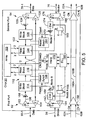
FIG. 2 provides details ofchip 30 according to some embodiments of the inventions, although various other details may be used.Receivers transmitters first port 92 andreceivers transmitters second port 94. Note that it is arbitrary which port to label the first port and which to label the second port.Transmitters receivers conductors 50 and conductor 70-1 is one ofconductors 70 ofFIG. 1 (although there might be only one data conductor per port).FIG. 2 also illustratesconductors FIG. 1 . In the embodiment ofFIG. 2 , the external clock signal (clk) ofFIG. 1 is a differential clock (Clk and Clk#), but it could be single ended.Conductors 62A and 62B. andconductor FIG. 1 . A high bandwidth, low jitter clock can help reduce jitter that could otherwise accumulate at each interface. To reduce jitter, in addition to providing the clock differentially, a low voltage swing may also be used. Further, as an example, receiver 186 andtransmitter 188 may include current-mode, differential amplifiers. The data and external strobe signals may be full voltage swing or low voltage swing signals. - The external differential clock signal (Clk, Clk#) is received by receiver 186 which drives the external differential clock signal on
conductors circuit 196 andtransmitter 188.Transmitter 188. drives the external differential clock signal toconductors 82A and 82B. to be received by another chip or perhaps to be terminated. Buffering provided by receiver 186 may be designed to provide high supply and common mode rejection and very small jitter.DLL circuit 196 locks to the buffered external differential clock signal and is selected to lock to a particular phase of the external differential clock signal (for example, 180° (degrees)) and to generate, for example, four equally spaced delays across a complete clock cycle at DLL taps. The spaced delays may be fed through the taps to aninterpolator 172 to produce, for example, an adjustable delay of 32 steps over 360°.Interpolator 172 provides a phase adjusted internal differential clock signal (Clk(I), Clk#(I)) throughbuffer 162 to a node A (although it could be single ended). The phase adjusted internal differential clock signal at node A is provided to readblocks synchronizers 158. and 164. - In some embodiments, the phase adjusted internal differential clock signal provides double data rate clocking for data signals passing between
array 100 and readblocks array 100 and read block 116 for each one ofconductors array 100 may operate at, for example, ½ the frequency of the port interfaces, so twice the number of conductors are used to get the same data. InFIG. 2 , the conductors betweenarray 100 and readblocks conductors 50 and 70) rather than two betweenarray 100 and each read blocks. - In some embodiments, the data signals on
conductors conductors - In response to detecting the data signals on conductors 50-1 and 70-1,
receivers buffers 108. and 134, which in turn provide the received data signals to writeblocks block 114. and read block 116 form a first-in first-out (FIFO) circuit in which data is written into the FIFO synchronously with the strobe signal at node B and is read out of the FIFO synchronously with the clock signal at node A. Likewise, in some embodiments, writeblock 126 and read block 124 form a FIFO circuit in which data is written into the FIFO synchronously with the strobe signal at node C and is read out of the FIFO synchronously with the clock signal at nodeA. Reset synchronizers - In some embodiments, the external strobe signals on
conductors delay circuits buffers FIG. 2 , the first and second received strobe signals are also delayed received strobe signals. The first and second received strobe signals then have a desired phase relationship with respect to received data signals received by the write blocks 114 and 126 frombuffers write blocks Buffers Buffers - The first received strobe signal is further delayed by
delay circuit 154 under the control ofDLL 196. to create a desired phase delay difference between nodes B and A, and hence between writing into and reading fromFIFO 112. An example of the desired minimum delay is 90°. In the example ofFIG. 2 , delay circuits 150,154, and 174 are low power consuming slave delay circuits controlled byDLL circuit 196 which acts as a master.Interpolator 172 receives the further delayed first received strobe signal fromdelay circuit 154 and at least part of the phase adjusted internal clock signal from node A and adjusts the phase adjusted internal clock signal to be in phase with the further delayed received strobe signal fromdelay circuit 154. Accordingly, in the example ofFIG. 2 , the first received strobe signal is the fixed phase received strobe signal and the second received strobe signal is the arbitrary phase received strobe signal. However, the circuitry ofFIG. 2 could be modified so that just the opposite were the case. In the example, the delay is 90° which leads to a low latency for those datapaths involving FIFO 112. The latency in data paths involving bothwrite block 126 and read block 124 is an arbitrary latency because data written intoFIFO 122 can take an arbitrary amount of time (within the limits discussed) to be read out. - In the example of
FIG. 2 , the following data paths are low latency data paths: - the path from conductor 50-1 through
receiver 102,buffer 108, writeblock 114, readblock 116, andtransmitter 138 toconductor 138; - the path from conductor 50-1. through
receiver 102,buffer 108, writeblock 114, read block 116 toarray 100; - the path from
array 100 to read block 116 totransmitter 138 to conductor 70-1; and - the path from
array 100 to read block 124 totransmitter 104 to conductor 50-1. - In the example of
FIG. 2 , the following are arbitrary latency data paths: - the path from conductor 70-1 through
receiver 136,buffer 134, writeblock 126, and read block 124 toarray 100; and - the path from conductor 70-1 through
receiver 136,buffer 134, writeblock 126, readblock 124, andtransmitter 104 to conductor 50-1. - As an example,
FIG. 3 shows the first received strobe signal at node B being 90° out of phase with the received data signal atwrite block 114.FIG. 4 . shows the second received strobe signal at node C being 90° out of phase with the received data signal atwrite block 126. InFIG. 3 , the phase adjusted internal clock signal at node A is 90° out of phase with the received strobe signal at node B. InFIG. 4 , the phase adjusted internal clock signal at node A is an arbitrary amount out of phase with the received strobe signal at node C. The arbitrary phase difference inFIG. 4 . is expressed as a desired minimum phase difference (for example 90°) + X°, where in X may be for example, 360°. In other embodiments, X might be some other amount such as 270° or 450°. In some embodiments,synchronizers synchronizer 158 does not have to add or remove phase difference. Although the desired minimum phase difference is mentioned as 90°, other amounts might be used such as 270° (that is, in 1.5 bit cells).. Note that the desired minimum phase difference and the additional delay X do not have to be multiples of 90°. - In some embodiments,
chip 30 transmits all the data signals that it receives fromchip 20 tochip 40. Chip. 30 also decides whether the data signals is to be used by chip 30 (for example, stored by chip 30) or are merely to be passed on tochip 40. Examples of techniques for deciding whetherchip 30 is to use the data include (1) having a particular portion of the data signal currently being received indicate how it is to be used, (2) having a portion of a data signal previously received indicate how a future data signal is to be used, or (3) using a separate chip select signal (not shown). In other embodiments,chip 30 will only pass on only some of the data signals it receives fromchip 20 tochip 40. However, passing on only some of the data signals may add significant complexity and/or delay. -
Strobe creation circuitry transmitter 144. The strobe creation may be constant or gated to occur only around the time data signals are to be driven bytransmitters -
FIG. 5 illustrates alternative circuitry to that ofFIG. 2 .FIG. 5 is likeFIG. 2 . except that the received strobe signal is provided fromreceiver 142 tointerpolator 172 and there is nodelay circuitry 154 between node B and interpolator. Various other alternatives could be used. -
FIG. 6 illustrates a system that is similar toFIG. 1 except that it includesconductors chips FIG. 7 is similar toFIG. 1 except that the clock signal passes fromchip 20 to chip 30 and fromchip 30 tochip 40. -
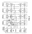
FIG. 8 illustrateschips FIG. 1 in a larger daisy chained point to point system wherechip 20 is a memory controller that provides data and strobe signals to memory chips M11, M21, M31, and M41 onmodule 1. Note that, in this example,chip 30 is chip M21 andchip 40 is chip. M22. Chips M11, M21, M31, and M41 repeat the data signals to memory chips M12, M22, M32, and M42 onmodule 2, which in turn repeat data signals to memory chips M13, M23, M33, and M43 onmodule 3, which in turn repeat the data signals to memory chips M14, M24, M34, and M44 onmodule 4. The chips regenerate strobe signals to send to these chips as discussed. Clock signals are provided bymemory controller 20 and are each passed on to one of the memory modules where they are distributed to memory chips. The clock signals could originate other than in the memory controller. The modules may be dual in line memory modules (DIMMs) or other types of modules.FIG. 9 is similar toFIG. 8 except that there are two modules rather than four.FIG. 8 illustrates four chips per module out of convenience for illustration, but there could be more than four memory chips per module and a single clock signal could be distributed to all the chips. In the case ofFIG. 9 , there could be more than eight memory chips per module. In actual systems, there could be more, less, or the same number of modules as is shown inFIGS. 8 and9 . Rings or other topologies than those shown inFIGS. 8 and9 may be used. For example, memory chips M14, M24, M34, and M44 may be coupled through conductors directly tomemory controller 20. - Jitter accumulation is a potential problem with the clock daisy-chained through multiple chips. The clock may set the baseline jitter for a chip and retime the data such that the maximum jitter in the chain be held to tolerable levels.
- The following is a discussion of exemplary techniques for SBD signaling. Referring to
FIG. 2 , an SBD signal can be created bytransmitter 104 driving a particular signal andreceiver 102 monitoring the voltage on conductor 50-1.Receiver 102 may subtract the voltage of the outgoing data from the voltage on conductor 50-1 to receive the incoming data signal. The amplifier may perform outbound subtraction by use of a pair of selectable reference voltages. The state of the output data signal is used to select the appropriate reference voltages, effecting a digital subtraction of the outbound data signal from the data signal present on conductor 50-1. The timing of the reference voltage change should be such as to match the output data fromtransmitter 102. Table 1 below shows an example for SBD signaling, where Vcc is the supply voltage for transmitters and receivers ofchips Table 1 (example of SBD signaling) Voltage driven by transmitter 104 to conductor 50-1Reference voltage of receiver 102Voltage driven by transmitter in chip 20 to conductor 50-1Output of receiver 102Logical high ¾ Vcc Logical high Logical high Logical high ¾ Vcc Logical low Logical low Logical low ¼ Vcc Logical high Logical high Logical low ¼ Vcc Logical low Logical low -
Transmitters transmitter 104 may perform as both a termination and a level translator betweenchip 30 and chip. 20 supply voltages. Referring toFIG. 10 , to perform the translation function, the logic power supply (chip 20 Vcc) may be connected to a p-type metal oxide semiconductor field effect transistor (PMOSFET) section of a push-pull transmitter 244 inchip 20, and drive one-half this supply voltage level. As the transmitters may also serve as terminators, tunable, binary weighted, complementary MOS (CMOS) push-pull transmitters chips Receivers - The inventions are not restricted to a particular type of receiver. In some embodiments,
receivers FIG. 11 , but this is not required. Referring toFIG. 11 ,receiver 102 may subtract the voltage of the outgoing data fromtransmitter 104 from the voltage on conductor 50-1 to receive the incoming data signal; be capable of operating over a wide range of input common mode levels; maintain high common-mode noise rejection; and provide amplification to convert the received signals to CMOS. levels. As shown in the example ofFIG. 11 ,receiver 102 may have three stages. The first stage may be based on a pair of complementary differential amplifiers and provide wide common-mode input range and common-mode noise rejection. The amplifier may perform outbound subtraction by use of a pair of selectable references RefHi and RefLo selected by signals HiSel and LoSel. The first stage may be further divided into four parallel segments to achieve staged, controlled switching between the two references in order to maintain a closely matched relationship with slew-rate controlled outbound data switching. The second stage amplifier may provide gain, common mode restoration, and combine the outputs of the first stage differential amplifiers into a single differential signal. The last stage may provide additional gain and convert the differential signal into a single-ended CMOS output atconductor 106. - There may be various additional circuitry that are not illustrated (for example, electrostatic discharge circuitry). There may be additional strobe and/or clock signals provided to the chips.
- An embodiment is an implementation or example of the inventions. Reference in the specification to "an embodiment," "one embodiment," "some embodiments," or "other embodiments" means that a particular feature, structure, or characteristic described in connection with the embodiments is included in at least some embodiments, but not necessarily all embodiments, of the inventions. The various appearances of "an embodiment," "one embodiment," or "some embodiments" are not necessarily all referring to the same embodiments.
- If the specification states a component, feature, structure, or characteristic "may", "might", or "could" be included, that particular component, feature, structure, or characteristic is not required to be included. If the specification or claim refers to "a" or "an" element, that does not mean there is only one of the element... If the specification or claims refer to "an additional" element, that does not preclude there being more than one of the additional element.
Claims (13)
- A chip (30) comprising:a memory array (100)a first port (92) to provide a first received data signal and a first received strobe signal, further comprising a first transmitter (104) for transmitting data;a second port (94) to provide a second received data signal and a second received strobe signal, further comprising a second transmitter (138) for transmitting data;circuitry (150,152,154,172,196) to provide an internal clock signal (Clk(I),Clk#(I)) with a fixed phase relationship to only the first received strobe signal;first and second write blocks (114,126) to latch the first and second received data signals synchronously with the first and second received strobe signals, respectively;a first read block (116) to be clocked by the internal clock, wherein the first read block interfaces between the first write block and the memory array, and interfaces between the memory array and a transmitter (138) of the second port; anda second read block (124) to be clocked by the internal clock, wherein the second read block interfaces between the second write block (126) and the memory array, and interfaces between the memory array and the first transmitter of the first port.
- The chip of claim 1, wherein the internal clock signal clocks data in the first and second read blocks at a double data rate.
- The chip of claim 1, wherein the internal clock signal is a phase adjusted internal clock signal and wherein the circuitry to provide the internal clock includes delayed locked loop circuitry (196) that receives a non-phase adjusted internal clock and provides timing signals to an interpolator (172) which produces the phase adjusted internal clock signal.
- The chip of claim 3, wherein the interpolator receives at least a portion of the phase adjusted internal clock signal as an input and receives a delayed received strobe signal as an input.
- The chip of claim 3, wherein the internal clock signal is a phase adjusted differential internal clock signal.
- The chip of claim 1, wherein the chip repeats data it receives from the first port to the second transmitter at the second port.
- A chip as claimed in claim 1 wherein the circuitry comprises means to provide a phase adjusted internal clock signal with a fixed phase relationship to the first received strobe signal comprising delay circuitry to delay the first received data strobe signal to latch the first received data signal and to delay the second received data strobe signal to latch the second received data signal.
- A system comprising:a first chip (20) and a second chip (40); anda third chip according to claim 1 (30) comprising:a memory array (100);a first port (92) coupled to first chip to provide a first received data signal and a first received strobe signal, further comprising a first transmitter (104) for transmitting data;a second port (94) coupled to second chip to provide a second received data signal and a second received strobe signal, further comprising a second transmitter (138) for transmitting data;circuitry (150,152,154,172,196) to provide an internal clock signal (Clk(I),Clk#(I)) with a fixed phase relationship to only the first received strobe signal;first and second write blocks (114,126) to latch the first and second received data signals synchronously with the first and second received strobe signals, respectively;a first read block to be clocked by the internal clock, wherein the first read block interfaces between the first write block and the memory array, and interfaces between the memory array and the transmitter of the second port; anda second read block to be clocked by the internal clock, wherein the second read block interfaces between the second write block and the memory array, and interfaces between the memory array and the transmitter of the first port.
- The system of claim 8, wherein the third chip repeats data that it receives from the first port to the second chip and data that it receives from the second port to the first chip.
- The system of claim 8, wherein the internal clock signal clocks data in the first and second read blocks at a double data rate.
- The system of claim 8, wherein the internal clock signal is a phase adjusted internal clock signal and wherein the circuitry to provide the internal clock includes delayed locked loop circuitry (196) that receives a non-phase adjusted internal clock and provides timing signals to an interpolator (172) which produces the phase adjusted internal clock signal.
- The system of claim 11, wherein the interpolator receives at least a portion of the phase adjusted internal clock signal as an input and receives a delayed received strobe signal as an input.
- The system of claim 8, wherein the signalling between the first and second chips and between the second and third chips is simultaneously bi-directional and the first received data signal and the first received strobe signal are provided responsive to a data signal and a strobe signal from the first chip, and the second received data signal and the second received strobe signal are provided responsive to a data signal and a strobe signal from the second chip.
Applications Claiming Priority (2)
| Application Number | Priority Date | Filing Date | Title |
|---|---|---|---|
| US10/749,677 US7031221B2 (en) | 2003-12-30 | 2003-12-30 | Fixed phase clock and strobe signals in daisy chained chips |
| PCT/US2004/043426 WO2005066966A1 (en) | 2003-12-30 | 2004-12-23 | Fixed phase clock and strobe signals in daisy chained chips |
Publications (2)
| Publication Number | Publication Date |
|---|---|
| EP1700308A1 EP1700308A1 (en) | 2006-09-13 |
| EP1700308B1 true EP1700308B1 (en) | 2009-09-30 |
Family
ID=34711113
Family Applications (1)
| Application Number | Title | Priority Date | Filing Date |
|---|---|---|---|
| EP04815495A Not-in-force EP1700308B1 (en) | 2003-12-30 | 2004-12-23 | Fixed phase clock and strobe signals in daisy chained chips |
Country Status (9)
| Country | Link |
|---|---|
| US (1) | US7031221B2 (en) |
| EP (1) | EP1700308B1 (en) |
| KR (1) | KR100806465B1 (en) |
| CN (1) | CN1890754B (en) |
| AT (1) | ATE444555T1 (en) |
| DE (1) | DE602004023423D1 (en) |
| HK (1) | HK1091941A1 (en) |
| TW (1) | TWI269950B (en) |
| WO (1) | WO2005066966A1 (en) |
Families Citing this family (59)
| Publication number | Priority date | Publication date | Assignee | Title |
|---|---|---|---|---|
| US7400670B2 (en) | 2004-01-28 | 2008-07-15 | Rambus, Inc. | Periodic calibration for communication channels by drift tracking |
| US7095789B2 (en) | 2004-01-28 | 2006-08-22 | Rambus, Inc. | Communication channel calibration for drift conditions |
| US8422568B2 (en) | 2004-01-28 | 2013-04-16 | Rambus Inc. | Communication channel calibration for drift conditions |
| US6961862B2 (en) * | 2004-03-17 | 2005-11-01 | Rambus, Inc. | Drift tracking feedback for communication channels |
| TWI460736B (en) * | 2005-09-30 | 2014-11-11 | Conversant Intellectual Property Man Inc | Independent link and bank selection |
| US20070076502A1 (en) | 2005-09-30 | 2007-04-05 | Pyeon Hong B | Daisy chain cascading devices |
| US11948629B2 (en) | 2005-09-30 | 2024-04-02 | Mosaid Technologies Incorporated | Non-volatile memory device with concurrent bank operations |
| US7747833B2 (en) | 2005-09-30 | 2010-06-29 | Mosaid Technologies Incorporated | Independent link and bank selection |
| WO2007036050A1 (en) | 2005-09-30 | 2007-04-05 | Mosaid Technologies Incorporated | Memory with output control |
| US7652922B2 (en) | 2005-09-30 | 2010-01-26 | Mosaid Technologies Incorporated | Multiple independent serial link memory |
| US7555670B2 (en) * | 2005-10-26 | 2009-06-30 | Intel Corporation | Clocking architecture using a bidirectional clock port |
| WO2007052212A1 (en) * | 2005-11-03 | 2007-05-10 | Nxp B.V. | Data interface and method of seeking synchronization |
| KR100870536B1 (en) | 2005-12-19 | 2008-11-26 | 삼성전자주식회사 | High speed interface semiconductor device, semiconductor system, and method there-of |
| US20070290333A1 (en) * | 2006-06-16 | 2007-12-20 | Intel Corporation | Chip stack with a higher power chip on the outside of the stack |
| DE102006036823B4 (en) * | 2006-08-07 | 2008-10-02 | Qimonda Ag | Data synchronization and buffer circuit for the synchronization of serially received data signals |
| EP2487794A3 (en) * | 2006-08-22 | 2013-02-13 | Mosaid Technologies Incorporated | Modular command structure for memory and memory system |
| US8407395B2 (en) * | 2006-08-22 | 2013-03-26 | Mosaid Technologies Incorporated | Scalable memory system |
| US7904639B2 (en) | 2006-08-22 | 2011-03-08 | Mosaid Technologies Incorporated | Modular command structure for memory and memory system |
| US7752364B2 (en) * | 2006-12-06 | 2010-07-06 | Mosaid Technologies Incorporated | Apparatus and method for communicating with semiconductor devices of a serial interconnection |
| US7925854B2 (en) * | 2006-12-06 | 2011-04-12 | Mosaid Technologies Incorporated | System and method of operating memory devices of mixed type |
| TWI457944B (en) * | 2006-12-06 | 2014-10-21 | Mosaid Technologies Inc | Apparatus, method and system for communicating with semiconductor devices of a serial interconnection |
| EP2118903A4 (en) * | 2006-12-06 | 2010-01-06 | Mosaid Technologies Inc | System and method of operating memory devices of mixed type |
| US8433874B2 (en) * | 2006-12-06 | 2013-04-30 | Mosaid Technologies Incorporated | Address assignment and type recognition of serially interconnected memory devices of mixed type |
| US7554855B2 (en) * | 2006-12-20 | 2009-06-30 | Mosaid Technologies Incorporated | Hybrid solid-state memory system having volatile and non-volatile memory |
| US8122202B2 (en) | 2007-02-16 | 2012-02-21 | Peter Gillingham | Reduced pin count interface |
| CN101617371B (en) | 2007-02-16 | 2014-03-26 | 莫塞德技术公司 | Non-volatile semiconductor memory having multiple external power supplies |
| US8086785B2 (en) | 2007-02-22 | 2011-12-27 | Mosaid Technologies Incorporated | System and method of page buffer operation for memory devices |
| US8046527B2 (en) | 2007-02-22 | 2011-10-25 | Mosaid Technologies Incorporated | Apparatus and method for using a page buffer of a memory device as a temporary cache |
| KR100885915B1 (en) * | 2007-02-27 | 2009-02-26 | 삼성전자주식회사 | Inter-communicating multi memory chip and system including the same |
| US7865756B2 (en) * | 2007-03-12 | 2011-01-04 | Mosaid Technologies Incorporated | Methods and apparatus for clock signal synchronization in a configuration of series-connected semiconductor devices |
| US7904859B2 (en) * | 2007-05-09 | 2011-03-08 | Synopsys, Inc. | Method and apparatus for determining a phase relationship between asynchronous clock signals |
| US7688652B2 (en) * | 2007-07-18 | 2010-03-30 | Mosaid Technologies Incorporated | Storage of data in memory via packet strobing |
| WO2009062280A1 (en) * | 2007-11-15 | 2009-05-22 | Mosaid Technologies Incorporated | Methods and systems for failure isolation and data recovery in a configuration of series-connected semiconductor devices |
| US8825939B2 (en) * | 2007-12-12 | 2014-09-02 | Conversant Intellectual Property Management Inc. | Semiconductor memory device suitable for interconnection in a ring topology |
| US8467486B2 (en) * | 2007-12-14 | 2013-06-18 | Mosaid Technologies Incorporated | Memory controller with flexible data alignment to clock |
| US8781053B2 (en) * | 2007-12-14 | 2014-07-15 | Conversant Intellectual Property Management Incorporated | Clock reproducing and timing method in a system having a plurality of devices |
| US8291248B2 (en) | 2007-12-21 | 2012-10-16 | Mosaid Technologies Incorporated | Non-volatile semiconductor memory device with power saving feature |
| US8145925B2 (en) * | 2007-12-21 | 2012-03-27 | Mosaid Technologies Incorporated | Non-volatile semiconductor memory device with power saving feature |
| US8594110B2 (en) | 2008-01-11 | 2013-11-26 | Mosaid Technologies Incorporated | Ring-of-clusters network topologies |
| US8139390B2 (en) * | 2008-07-08 | 2012-03-20 | Mosaid Technologies Incorporated | Mixed data rates in memory devices and systems |
| US8181056B2 (en) * | 2008-09-30 | 2012-05-15 | Mosaid Technologies Incorporated | Serial-connected memory system with output delay adjustment |
| US8161313B2 (en) * | 2008-09-30 | 2012-04-17 | Mosaid Technologies Incorporated | Serial-connected memory system with duty cycle correction |
| US8134852B2 (en) * | 2008-10-14 | 2012-03-13 | Mosaid Technologies Incorporated | Bridge device architecture for connecting discrete memory devices to a system |
| US7957173B2 (en) * | 2008-10-14 | 2011-06-07 | Mosaid Technologies Incorporated | Composite memory having a bridging device for connecting discrete memory devices to a system |
| US8549209B2 (en) * | 2008-11-04 | 2013-10-01 | Mosaid Technologies Incorporated | Bridging device having a configurable virtual page size |
| US20100115172A1 (en) * | 2008-11-04 | 2010-05-06 | Mosaid Technologies Incorporated | Bridge device having a virtual page buffer |
| US8194481B2 (en) | 2008-12-18 | 2012-06-05 | Mosaid Technologies Incorporated | Semiconductor device with main memory unit and auxiliary memory unit requiring preset operation |
| US8037235B2 (en) * | 2008-12-18 | 2011-10-11 | Mosaid Technologies Incorporated | Device and method for transferring data to a non-volatile memory device |
| US8521980B2 (en) * | 2009-07-16 | 2013-08-27 | Mosaid Technologies Incorporated | Simultaneous read and write data transfer |
| KR101086875B1 (en) | 2009-09-30 | 2011-11-25 | 주식회사 하이닉스반도체 | Data transmission circuit and semiconductor apparatus including the same |
| US8284621B2 (en) * | 2010-02-15 | 2012-10-09 | International Business Machines Corporation | Strobe offset in bidirectional memory strobe configurations |
| US8582382B2 (en) * | 2010-03-23 | 2013-11-12 | Mosaid Technologies Incorporated | Memory system having a plurality of serially connected devices |
| US8825967B2 (en) | 2011-12-08 | 2014-09-02 | Conversant Intellectual Property Management Inc. | Independent write and read control in serially-connected devices |
| US9471484B2 (en) | 2012-09-19 | 2016-10-18 | Novachips Canada Inc. | Flash memory controller having dual mode pin-out |
| TWI493566B (en) * | 2012-10-15 | 2015-07-21 | Via Tech Inc | Data storage device, and storage media controller and control method |
| US9571908B2 (en) * | 2014-12-23 | 2017-02-14 | Raytheon Company | Extendable synchronous low power telemetry system for distributed sensors |
| US10431268B2 (en) | 2016-09-13 | 2019-10-01 | Samsung Electronics Co., Ltd. | Semiconductor device and memory controller receiving differential signal |
| US10635357B2 (en) | 2018-07-03 | 2020-04-28 | Nvidia Corporation | Method for overlapping memory accesses |
| KR20200051291A (en) * | 2018-11-05 | 2020-05-13 | 에스케이하이닉스 주식회사 | Semiconductor Apparatus and Semiconductor System and Operating Method Using the same |
Family Cites Families (18)
| Publication number | Priority date | Publication date | Assignee | Title |
|---|---|---|---|---|
| US112119A (en) * | 1871-02-28 | Improvement in self-centering chucks for lathes | ||
| US6570944B2 (en) * | 2001-06-25 | 2003-05-27 | Rambus Inc. | Apparatus for data recovery in a synchronous chip-to-chip system |
| US5195056A (en) * | 1987-05-21 | 1993-03-16 | Texas Instruments, Incorporated | Read/write memory having an on-chip input data register, having pointer circuits between a serial data register and input/output buffer circuits |
| JPH04216392A (en) * | 1990-12-18 | 1992-08-06 | Mitsubishi Electric Corp | Semiconductor storage device provided with block write function |
| US5546023A (en) * | 1995-06-26 | 1996-08-13 | Intel Corporation | Daisy chained clock distribution scheme |
| US5604450A (en) * | 1995-07-27 | 1997-02-18 | Intel Corporation | High speed bidirectional signaling scheme |
| US7024518B2 (en) | 1998-02-13 | 2006-04-04 | Intel Corporation | Dual-port buffer-to-memory interface |
| US6742098B1 (en) * | 2000-10-03 | 2004-05-25 | Intel Corporation | Dual-port buffer-to-memory interface |
| US6697888B1 (en) * | 2000-09-29 | 2004-02-24 | Intel Corporation | Buffering and interleaving data transfer between a chipset and memory modules |
| US6658509B1 (en) * | 2000-10-03 | 2003-12-02 | Intel Corporation | Multi-tier point-to-point ring memory interface |
| US6934785B2 (en) * | 2000-12-22 | 2005-08-23 | Micron Technology, Inc. | High speed interface with looped bus |
| US6437601B1 (en) * | 2000-12-26 | 2002-08-20 | Intel Corporation | Using a timing strobe for synchronization and validation in a digital logic device |
| US6373289B1 (en) * | 2000-12-26 | 2002-04-16 | Intel Corporation | Data and strobe repeater having a frequency control unit to re-time the data and reject delay variation in the strobe |
| US6493250B2 (en) * | 2000-12-28 | 2002-12-10 | Intel Corporation | Multi-tier point-to-point buffered memory interface |
| US6832325B2 (en) * | 2000-12-29 | 2004-12-14 | Intel Corporation | Device on a source synchronous bus sending data in quadrature phase relationship and receiving data in phase with the bus clock signal |
| US6747474B2 (en) * | 2001-02-28 | 2004-06-08 | Intel Corporation | Integrated circuit stubs in a point-to-point system |
| US6847617B2 (en) | 2001-03-26 | 2005-01-25 | Intel Corporation | Systems for interchip communication |
| US6536025B2 (en) * | 2001-05-14 | 2003-03-18 | Intel Corporation | Receiver deskewing of multiple source synchronous bits from a parallel bus |
-
2003
- 2003-12-30 US US10/749,677 patent/US7031221B2/en not_active Expired - Fee Related
-
2004
- 2004-12-23 EP EP04815495A patent/EP1700308B1/en not_active Not-in-force
- 2004-12-23 DE DE602004023423T patent/DE602004023423D1/en active Active
- 2004-12-23 CN CN2004800368450A patent/CN1890754B/en not_active Expired - Fee Related
- 2004-12-23 WO PCT/US2004/043426 patent/WO2005066966A1/en not_active Application Discontinuation
- 2004-12-23 AT AT04815495T patent/ATE444555T1/en not_active IP Right Cessation
- 2004-12-23 KR KR1020067013080A patent/KR100806465B1/en not_active IP Right Cessation
- 2004-12-24 TW TW093140506A patent/TWI269950B/en not_active IP Right Cessation
-
2006
- 2006-10-10 HK HK06111135.7A patent/HK1091941A1/en not_active IP Right Cessation
Also Published As
| Publication number | Publication date |
|---|---|
| CN1890754A (en) | 2007-01-03 |
| CN1890754B (en) | 2010-05-26 |
| HK1091941A1 (en) | 2007-01-26 |
| US7031221B2 (en) | 2006-04-18 |
| TWI269950B (en) | 2007-01-01 |
| WO2005066966A1 (en) | 2005-07-21 |
| DE602004023423D1 (en) | 2009-11-12 |
| KR100806465B1 (en) | 2008-02-21 |
| KR20060101786A (en) | 2006-09-26 |
| EP1700308A1 (en) | 2006-09-13 |
| TW200525319A (en) | 2005-08-01 |
| US20050146980A1 (en) | 2005-07-07 |
| ATE444555T1 (en) | 2009-10-15 |
Similar Documents
| Publication | Publication Date | Title |
|---|---|---|
| EP1700308B1 (en) | Fixed phase clock and strobe signals in daisy chained chips | |
| US11410712B2 (en) | Memory system and data transmission method | |
| US6603686B2 (en) | Semiconductor memory device having different data rates in read operation and write operation | |
| US7013359B1 (en) | High speed memory interface system and method | |
| CN100452787C (en) | High speed signaling for interfacing VLSI CMOS circuits | |
| US7009428B2 (en) | High speed source synchronous signaling for interfacing VLSI CMOS circuits to transmission lines | |
| JP4063392B2 (en) | Signal transmission system | |
| US20170177301A1 (en) | Asymmetric chip-to-chip interconnect | |
| US20070260778A1 (en) | Memory controller with bi-directional buffer for achieving high speed capability and related method thereof | |
| US11025255B2 (en) | Signal generation circuit synchronized with a clock signal and a semiconductor apparatus using the same | |
| US8332680B2 (en) | Methods and systems for operating memory in two modes | |
| US8037338B2 (en) | Data interface method and apparatus | |
| JP4481326B2 (en) | Signal transmission system | |
| US7826303B2 (en) | Data output circuit having shared data output control unit | |
| US10419202B2 (en) | Serializer, data transmitting circuit, semiconductor apparatus and system including the same | |
| US10305500B1 (en) | Amplification circuit, and frequency dividing circuit, semiconductor apparatus and semiconductor system including the amplification circuit and or frequency dividing circuit | |
| KR20020091821A (en) | Signal reception curcuit, semiconductor apparatus and system | |
| KR20090045568A (en) | Multi-port memory device having serial i/o interface | |
| JP4477372B2 (en) | Signal processing circuit | |
| US20090180335A1 (en) | Integrated circuit with reduced pointer uncertainly | |
| KR100684890B1 (en) | Serdes system | |
| KR20170057917A (en) | Serilizer Comprising Feedback Circuit |
Legal Events
| Date | Code | Title | Description |
|---|---|---|---|
| PUAI | Public reference made under article 153(3) epc to a published international application that has entered the european phase |
Free format text: ORIGINAL CODE: 0009012 |
|
| 17P | Request for examination filed |
Effective date: 20060726 |
|
| AK | Designated contracting states |
Kind code of ref document: A1 Designated state(s): AT BE BG CH CY CZ DE DK EE ES FI FR GB GR HU IE IS IT LI LT LU MC NL PL PT RO SE SI SK TR |
|
| 17Q | First examination report despatched |
Effective date: 20061017 |
|
| REG | Reference to a national code |
Ref country code: HK Ref legal event code: DE Ref document number: 1091941 Country of ref document: HK |
|
| DAX | Request for extension of the european patent (deleted) | ||
| GRAP | Despatch of communication of intention to grant a patent |
Free format text: ORIGINAL CODE: EPIDOSNIGR1 |
|
| GRAS | Grant fee paid |
Free format text: ORIGINAL CODE: EPIDOSNIGR3 |
|
| GRAA | (expected) grant |
Free format text: ORIGINAL CODE: 0009210 |
|
| AK | Designated contracting states |
Kind code of ref document: B1 Designated state(s): AT BE BG CH CY CZ DE DK EE ES FI FR GB GR HU IE IS IT LI LT LU MC NL PL PT RO SE SI SK TR |
|
| REG | Reference to a national code |
Ref country code: CH Ref legal event code: EP Ref country code: GB Ref legal event code: FG4D |
|
| REG | Reference to a national code |
Ref country code: IE Ref legal event code: FG4D |
|
| REF | Corresponds to: |
Ref document number: 602004023423 Country of ref document: DE Date of ref document: 20091112 Kind code of ref document: P |
|
| REG | Reference to a national code |
Ref country code: HK Ref legal event code: GR Ref document number: 1091941 Country of ref document: HK |
|
| PG25 | Lapsed in a contracting state [announced via postgrant information from national office to epo] |
Ref country code: FI Free format text: LAPSE BECAUSE OF FAILURE TO SUBMIT A TRANSLATION OF THE DESCRIPTION OR TO PAY THE FEE WITHIN THE PRESCRIBED TIME-LIMIT Effective date: 20090930 Ref country code: LT Free format text: LAPSE BECAUSE OF FAILURE TO SUBMIT A TRANSLATION OF THE DESCRIPTION OR TO PAY THE FEE WITHIN THE PRESCRIBED TIME-LIMIT Effective date: 20090930 Ref country code: SE Free format text: LAPSE BECAUSE OF FAILURE TO SUBMIT A TRANSLATION OF THE DESCRIPTION OR TO PAY THE FEE WITHIN THE PRESCRIBED TIME-LIMIT Effective date: 20090930 |
|
| LTIE | Lt: invalidation of european patent or patent extension |
Effective date: 20090930 |
|
| PG25 | Lapsed in a contracting state [announced via postgrant information from national office to epo] |
Ref country code: PL Free format text: LAPSE BECAUSE OF FAILURE TO SUBMIT A TRANSLATION OF THE DESCRIPTION OR TO PAY THE FEE WITHIN THE PRESCRIBED TIME-LIMIT Effective date: 20090930 Ref country code: SI Free format text: LAPSE BECAUSE OF FAILURE TO SUBMIT A TRANSLATION OF THE DESCRIPTION OR TO PAY THE FEE WITHIN THE PRESCRIBED TIME-LIMIT Effective date: 20090930 |
|
| NLV1 | Nl: lapsed or annulled due to failure to fulfill the requirements of art. 29p and 29m of the patents act | ||
| PG25 | Lapsed in a contracting state [announced via postgrant information from national office to epo] |
Ref country code: RO Free format text: LAPSE BECAUSE OF FAILURE TO SUBMIT A TRANSLATION OF THE DESCRIPTION OR TO PAY THE FEE WITHIN THE PRESCRIBED TIME-LIMIT Effective date: 20090930 Ref country code: EE Free format text: LAPSE BECAUSE OF FAILURE TO SUBMIT A TRANSLATION OF THE DESCRIPTION OR TO PAY THE FEE WITHIN THE PRESCRIBED TIME-LIMIT Effective date: 20090930 Ref country code: PT Free format text: LAPSE BECAUSE OF FAILURE TO SUBMIT A TRANSLATION OF THE DESCRIPTION OR TO PAY THE FEE WITHIN THE PRESCRIBED TIME-LIMIT Effective date: 20100201 Ref country code: ES Free format text: LAPSE BECAUSE OF FAILURE TO SUBMIT A TRANSLATION OF THE DESCRIPTION OR TO PAY THE FEE WITHIN THE PRESCRIBED TIME-LIMIT Effective date: 20100110 Ref country code: IS Free format text: LAPSE BECAUSE OF FAILURE TO SUBMIT A TRANSLATION OF THE DESCRIPTION OR TO PAY THE FEE WITHIN THE PRESCRIBED TIME-LIMIT Effective date: 20100130 Ref country code: CZ Free format text: LAPSE BECAUSE OF FAILURE TO SUBMIT A TRANSLATION OF THE DESCRIPTION OR TO PAY THE FEE WITHIN THE PRESCRIBED TIME-LIMIT Effective date: 20090930 |
|
| PG25 | Lapsed in a contracting state [announced via postgrant information from national office to epo] |
Ref country code: CY Free format text: LAPSE BECAUSE OF FAILURE TO SUBMIT A TRANSLATION OF THE DESCRIPTION OR TO PAY THE FEE WITHIN THE PRESCRIBED TIME-LIMIT Effective date: 20090930 Ref country code: SK Free format text: LAPSE BECAUSE OF FAILURE TO SUBMIT A TRANSLATION OF THE DESCRIPTION OR TO PAY THE FEE WITHIN THE PRESCRIBED TIME-LIMIT Effective date: 20090930 |
|
| PG25 | Lapsed in a contracting state [announced via postgrant information from national office to epo] |
Ref country code: BE Free format text: LAPSE BECAUSE OF FAILURE TO SUBMIT A TRANSLATION OF THE DESCRIPTION OR TO PAY THE FEE WITHIN THE PRESCRIBED TIME-LIMIT Effective date: 20090930 Ref country code: AT Free format text: LAPSE BECAUSE OF FAILURE TO SUBMIT A TRANSLATION OF THE DESCRIPTION OR TO PAY THE FEE WITHIN THE PRESCRIBED TIME-LIMIT Effective date: 20090930 |
|
| PG25 | Lapsed in a contracting state [announced via postgrant information from national office to epo] |
Ref country code: DK Free format text: LAPSE BECAUSE OF FAILURE TO SUBMIT A TRANSLATION OF THE DESCRIPTION OR TO PAY THE FEE WITHIN THE PRESCRIBED TIME-LIMIT Effective date: 20090930 Ref country code: MC Free format text: LAPSE BECAUSE OF NON-PAYMENT OF DUE FEES Effective date: 20100701 Ref country code: NL Free format text: LAPSE BECAUSE OF FAILURE TO SUBMIT A TRANSLATION OF THE DESCRIPTION OR TO PAY THE FEE WITHIN THE PRESCRIBED TIME-LIMIT Effective date: 20090930 |
|
| REG | Reference to a national code |
Ref country code: CH Ref legal event code: PL |
|
| PLBE | No opposition filed within time limit |
Free format text: ORIGINAL CODE: 0009261 |
|
| STAA | Information on the status of an ep patent application or granted ep patent |
Free format text: STATUS: NO OPPOSITION FILED WITHIN TIME LIMIT |
|
| 26N | No opposition filed |
Effective date: 20100701 |
|
| REG | Reference to a national code |
Ref country code: FR Ref legal event code: ST Effective date: 20100831 |
|
| PG25 | Lapsed in a contracting state [announced via postgrant information from national office to epo] |
Ref country code: IE Free format text: LAPSE BECAUSE OF NON-PAYMENT OF DUE FEES Effective date: 20091223 Ref country code: LI Free format text: LAPSE BECAUSE OF NON-PAYMENT OF DUE FEES Effective date: 20091231 Ref country code: FR Free format text: LAPSE BECAUSE OF NON-PAYMENT OF DUE FEES Effective date: 20091231 Ref country code: CH Free format text: LAPSE BECAUSE OF NON-PAYMENT OF DUE FEES Effective date: 20091231 Ref country code: GR Free format text: LAPSE BECAUSE OF FAILURE TO SUBMIT A TRANSLATION OF THE DESCRIPTION OR TO PAY THE FEE WITHIN THE PRESCRIBED TIME-LIMIT Effective date: 20091231 |
|
| PG25 | Lapsed in a contracting state [announced via postgrant information from national office to epo] |
Ref country code: IT Free format text: LAPSE BECAUSE OF FAILURE TO SUBMIT A TRANSLATION OF THE DESCRIPTION OR TO PAY THE FEE WITHIN THE PRESCRIBED TIME-LIMIT Effective date: 20090930 Ref country code: BG Free format text: LAPSE BECAUSE OF FAILURE TO SUBMIT A TRANSLATION OF THE DESCRIPTION OR TO PAY THE FEE WITHIN THE PRESCRIBED TIME-LIMIT Effective date: 20091231 |
|
| PG25 | Lapsed in a contracting state [announced via postgrant information from national office to epo] |
Ref country code: LU Free format text: LAPSE BECAUSE OF NON-PAYMENT OF DUE FEES Effective date: 20091223 |
|
| PG25 | Lapsed in a contracting state [announced via postgrant information from national office to epo] |
Ref country code: HU Free format text: LAPSE BECAUSE OF FAILURE TO SUBMIT A TRANSLATION OF THE DESCRIPTION OR TO PAY THE FEE WITHIN THE PRESCRIBED TIME-LIMIT Effective date: 20100401 |
|
| PG25 | Lapsed in a contracting state [announced via postgrant information from national office to epo] |
Ref country code: TR Free format text: LAPSE BECAUSE OF FAILURE TO SUBMIT A TRANSLATION OF THE DESCRIPTION OR TO PAY THE FEE WITHIN THE PRESCRIBED TIME-LIMIT Effective date: 20090930 |
|
| PGFP | Annual fee paid to national office [announced via postgrant information from national office to epo] |
Ref country code: GB Payment date: 20171220 Year of fee payment: 14 |
|
| PGFP | Annual fee paid to national office [announced via postgrant information from national office to epo] |
Ref country code: DE Payment date: 20171220 Year of fee payment: 14 |
|
| REG | Reference to a national code |
Ref country code: DE Ref legal event code: R119 Ref document number: 602004023423 Country of ref document: DE |
|
| GBPC | Gb: european patent ceased through non-payment of renewal fee |
Effective date: 20181223 |
|
| PG25 | Lapsed in a contracting state [announced via postgrant information from national office to epo] |
Ref country code: DE Free format text: LAPSE BECAUSE OF NON-PAYMENT OF DUE FEES Effective date: 20190702 |
|
| PG25 | Lapsed in a contracting state [announced via postgrant information from national office to epo] |
Ref country code: GB Free format text: LAPSE BECAUSE OF NON-PAYMENT OF DUE FEES Effective date: 20181223 |