CN100452787C - High speed signaling for interfacing VLSI CMOS circuits - Google Patents
High speed signaling for interfacing VLSI CMOS circuits Download PDFInfo
- Publication number
- CN100452787C CN100452787C CNB998051551A CN99805155A CN100452787C CN 100452787 C CN100452787 C CN 100452787C CN B998051551 A CNB998051551 A CN B998051551A CN 99805155 A CN99805155 A CN 99805155A CN 100452787 C CN100452787 C CN 100452787C
- Authority
- CN
- China
- Prior art keywords
- signal
- ssvtr
- receiver
- comparator
- output
- Prior art date
- Legal status (The legal status is an assumption and is not a legal conclusion. Google has not performed a legal analysis and makes no representation as to the accuracy of the status listed.)
- Expired - Lifetime
Links
Images


Classifications
-
- H—ELECTRICITY
- H04—ELECTRIC COMMUNICATION TECHNIQUE
- H04L—TRANSMISSION OF DIGITAL INFORMATION, e.g. TELEGRAPHIC COMMUNICATION
- H04L25/00—Baseband systems
- H04L25/02—Details ; arrangements for supplying electrical power along data transmission lines
- H04L25/0264—Arrangements for coupling to transmission lines
- H04L25/028—Arrangements specific to the transmitter end
-
- H—ELECTRICITY
- H03—ELECTRONIC CIRCUITRY
- H03K—PULSE TECHNIQUE
- H03K19/00—Logic circuits, i.e. having at least two inputs acting on one output; Inverting circuits
- H03K19/0175—Coupling arrangements; Interface arrangements
- H03K19/0185—Coupling arrangements; Interface arrangements using field effect transistors only
- H03K19/018585—Coupling arrangements; Interface arrangements using field effect transistors only programmable
-
- H—ELECTRICITY
- H03—ELECTRONIC CIRCUITRY
- H03M—CODING; DECODING; CODE CONVERSION IN GENERAL
- H03M9/00—Parallel/series conversion or vice versa
-
- H—ELECTRICITY
- H04—ELECTRIC COMMUNICATION TECHNIQUE
- H04L—TRANSMISSION OF DIGITAL INFORMATION, e.g. TELEGRAPHIC COMMUNICATION
- H04L25/00—Baseband systems
- H04L25/02—Details ; arrangements for supplying electrical power along data transmission lines
- H04L25/0264—Arrangements for coupling to transmission lines
- H04L25/0278—Arrangements for impedance matching
-
- H—ELECTRICITY
- H04—ELECTRIC COMMUNICATION TECHNIQUE
- H04L—TRANSMISSION OF DIGITAL INFORMATION, e.g. TELEGRAPHIC COMMUNICATION
- H04L25/00—Baseband systems
- H04L25/02—Details ; arrangements for supplying electrical power along data transmission lines
- H04L25/0264—Arrangements for coupling to transmission lines
- H04L25/0292—Arrangements specific to the receiver end
-
- H—ELECTRICITY
- H04—ELECTRIC COMMUNICATION TECHNIQUE
- H04L—TRANSMISSION OF DIGITAL INFORMATION, e.g. TELEGRAPHIC COMMUNICATION
- H04L25/00—Baseband systems
- H04L25/02—Details ; arrangements for supplying electrical power along data transmission lines
- H04L25/06—Dc level restoring means; Bias distortion correction ; Decision circuits providing symbol by symbol detection
- H04L25/061—Dc level restoring means; Bias distortion correction ; Decision circuits providing symbol by symbol detection providing hard decisions only; arrangements for tracking or suppressing unwanted low frequency components, e.g. removal of dc offset
-
- H—ELECTRICITY
- H04—ELECTRIC COMMUNICATION TECHNIQUE
- H04L—TRANSMISSION OF DIGITAL INFORMATION, e.g. TELEGRAPHIC COMMUNICATION
- H04L7/00—Arrangements for synchronising receiver with transmitter
- H04L7/0008—Synchronisation information channels, e.g. clock distribution lines
-
- H—ELECTRICITY
- H04—ELECTRIC COMMUNICATION TECHNIQUE
- H04L—TRANSMISSION OF DIGITAL INFORMATION, e.g. TELEGRAPHIC COMMUNICATION
- H04L25/00—Baseband systems
- H04L25/02—Details ; arrangements for supplying electrical power along data transmission lines
- H04L25/0264—Arrangements for coupling to transmission lines
- H04L25/0272—Arrangements for coupling to multiple lines, e.g. for differential transmission
Abstract
A system of the present invention uses small swing differential source synchronous voltage and timing reference (SSVTR and /SSVTR) signals to compare single-ended signals of the same slew rate generated at the same time from the same integrated circuit for high frequency signaling. The SSVTR and /SSVTR signals toggle every time the valid signals are driven by the transmitting integrated circuit. Each signal receiver includes two comparators, one for comparing the signal against SSVTR and the other for comparing the signal against /SSVTR. A present signal binary value determines which comparator is coupled to the receiver output, optionally by using XOR logic with SSVTR and /SSVTR. The coupled comparator in the receiver detects whether change in signal binary value occurred or not until SSVTR and /SSVTR have changed their binary value. The same comparator is coupled if the signal transitions. The comparator is de-coupled if no transition occurs. The system may use a first set of oscillating references on a first bus for detecting transitions in control information and a second set of oscillating references for detecting transitions in data information.
Description
Technical field:
The present invention relates generally to the trusted computer signal communication, relate in particular to a kind of integrated circuit interface and method of communicating by letter of being used in a kind of high speed block movement with the bus that reduces power consumption or data, control and address signal between the multiple ic in the point-to-point connection.
Background technology:
The semiconductor integrated circuit that uses in numerical calculation and other digital application often uses a plurality of ultra-large integrated (VLSI) interconnection circuit to be used for striding across single hop or the multistage transmission line is realized binary signaling.Conventional transmission line comprises figure (Traces), and they are formed on for example a kind of printed circuit board (PCB) of a kind of suitable substrate.Each transmission line can be designed, and for example, uses so-called micro-strip pattern and strip line figure so that form a kind of transmission line with the characteristic impedance that is approximately 50-70 ohm.On the other hand, each transmission line can have the opposite end with their characteristic impedance terminating.Can be low in the output loading that is used on the driver of this transmission line as 25-35 ohm.
In order to consume rational power, high-frequency signal transmission requires little amplitude signal.Looking like radio transistor-transistor logic circuit (GTL) for a kind of, high speed transistor logical circuit (HSTL), detect the receiver of variation (for example 0.8-1.2V) in the such noisy environment of SSTL or RAMBUS easily, electric current is very big (for example each driver is approximately the 50-60 milliampere) also.A kind of typical receiver uses a kind of comparator with reference voltage (VREF) signal that forms between input high pressure (VIH) and input low pressure (VIL).Vref signal is a kind of high impedance DC (direct current) reference voltage, at inaccuracy ground tracking power supply of whole time, but can not respond transient noise.Routinely, the signal that high output voltage (VOH) and low output voltage (VOL) representative form from emission source, and VIL and VIH representative arrive the signal of the input of this receiving equipment, although they may be considered to identical signal.
Figure 1A is the block diagram that a kind of prior art receiver 10 of RAMBUS technology is used in explanation.This system 10 comprises one via the attenuator 100 of signal line 103 with inner input receiver 110 couplings.Vref signal 105 and each inner receiver 110 coupling.VREF produces from power supply.Usually, the DC value of this power supply has 5% change.Figure 1B is sequential Figure 125 of the explanation example signal relevant with low reference voltage (VREFl) with high reference voltage (VREFh).The value of VREFh and VREFl generally depends on the power source change that often produces vref signal in the past.For detection signal polarity reliably, require big variation, i.e. difference between high-voltage signal (VIH) and the low-voltage signal (VIL) and more than vref signal and following stable signal level.The variation of existing single-ended signal transmission technology is approximately 0.8V routinely.
Fig. 1 C is a block diagram that the schematic diagram of the prior art receiver 150 that uses the RAMBUS technology is described.150 pairs of input signals 167 of this receiver and vref signal 154 are sampled and are reached a kind of stable level up to this signal, and at this moment transmission gate 160 and 165 is closed.In case transmission gate 160 and 165 is closed, detecting gate 172 just can be eliminated electric current and inject.Fig. 1 D is sequential Figure 175 of the operation of the explanation receiver 150 that is used for a kind of example signal.150 pairs of input reference signals of this receiver and input signal sampling reach a kind of stable level up to this signal, for example a kind of low logic level (VIL), and when input signal is stablized, this receiver will be read this input signal values.As mentioned above, for carrying out input reliably, this signal voltage skew must be near being enough to allow all receivers 150 with a kind of stable signal of enough surplus sampling that is used for settling time and retention time.This variation should occur in less than departing from (skew) time so that allow to be used for signal in 30% time minimum period, the surplus of settling time and retention time.In a kind of big capacity loading environment that is operated in high frequency, when in this driver current, having under the situation of additional load, when time minimum period is reduced to below 1 millisecond, is used for signal and departs from the time, the surplus of settling time and retention time also will reduce.The low-voltage differential signal transmission of being used by IEEE P1596.3 (LVDS) can overcome these problems as cost by using the 250mv variation with operation greeting signal.Signal is greeted in operation must be increased number of leads and increase size of components.
In addition, computer system is generally used a kind of bus system, and in this system, some equipment are connected to this bus.Great majority in them use clock so that make data-signal, and address and control signal come into force.Figure 21 illustrates a kind of prior art systems 2100 that is used for direct ram bus dynamic random access memory (DRDRAM), and this system uses a kind of clock line 2130 with two sections (segment) 2136 and 2138.One section 2136 end from this data/address bus extends to a turning point 2137 near this bus second end.Another clock section 2138 oppositely extends to first end of this data/address bus from turning point 2137.This signal bus 2120 data signal, address and control signal.When this clock 2132 is used by this equipment so that when receiving a certain signal, this topological structure guarantees that this signal that sends appears at same direction transmission all the time synchronously on this bus 2120.If all signals that loaded almost are identical with clock, and this clock 2132 be used for the sampling and receive this signal, this work is very successful so.But this system may require to double this data bandwidth sometimes, in this case, even the address is identical with control signal, and can be shared, and this class bus system also needs number of signals is doubled.
Therefore, in the prior art that is used for low-cost VLSI digital system, need low-power driver and receiver reliably for the high-frequency operation of a large amount of single-ended signals.
Summary of the invention:
A system of the present invention use little skew (swing) differential source synchronizing voltage and timing reference signal (SSVTR with/SSVTR) so that the single-ended signal of the same offset that from the identical integrated circuit of high-frequency signal transmission, produces relatively."/" is used to represent logic NOT (NOT).Be terminated in of the characteristic impedance of all signals of transmission line two ends with them.Each SSVTR and/when SSVTR triggered, useful signal was driven by this emission integrated circuit.Each signal receiver comprises two comparators, and one is used for this signal and SSVTR relatively, and another be used for this signal with/SSVTR relatively.The binary value of a current demand signal randomly determine which comparator by use XOR and SSVTR and/SSVTR is coupled.Up to SSVTR and/before SSVTR changed their binary value, whether the comparator detection signal binary value that is connected in this receiver changed.People understand again each SSVTR and/when SSVTR changed their binary value, this signal can change its binary value.SSVTR and/SSVTR preferably and this signal Synchronization.
Method of the present invention may further comprise the steps, obtain an oscillation source synchronizing voltage and timing reference signal and it complementary signal (SSVTR and/SSVTR), and receive a single-ended signal that enters.This method is compared the oscillating voltage reference signal so that produce first result with first comparator with the signal that enters, with second comparator with complementary signal and the signal comparison that enters so that produce second result.Then, this method selects a conduct among first result or second result based on an output signal with front signal.Select one of this result's step comprise with this output signal and reference signal (SSVTR) and complementary signal (/SSVTR) compare.Select step further be included on the basis of the current comparator that is coupled from before signal towards first or second this output signal of results operation.If the signal that enters changes, this selection step comprises keeps the identical comparator that is coupled.If the signal that enters keeps identical signal, this selection step comprises the current comparator that is coupled of decoupling, connects other comparator then.This method just allows this circuit stable at that time.
This system and method helps to cancel the needs to the high impedance vref signal that is used for smaller skew single-ended signal.This will make needed three different voltage levels (output high level, output low level and VREF level) reduce to two different voltage levels (output high level and output low level).Cancellation VREF will reduce necessary variation, thereby reduce power consumption.When this signal when each cycle is changed, use receiver to allow this receiver to be coupled with identical comparator with dual comparator.According to the current binary value of this signal and SSVTR, have only a comparator to be coupled.This system has a kind of adjustable seriatim delay makes each receiver be coupled or decoupling to this comparator, therefore, can reduce to depart from effect between the transmission period of source synchronizing signal.This system has multichannel differential source synchronizing voltage with the timing reference signal so that to comparing such as the multichannel single-ended signal in the identical integrated circuit of microprocessor with many signals or system controller.This system and method can help providing differential signal transmission in the single-ended signal transmission system.
Use same notion, this system can have two-way complementary auxiliary source synchronizing voltage and timing reference signal so that the comparison bidirectional single ended signal.This system can have a driver or transmitter accounts for the conversion of signals speed of major part so that be controlled at the whole signal period, thereby reduces output current.This system can have as the P-raceway groove of pull-up resistor or grounded-grid the internal driving match circuit in case between CPU and the cache or the characteristic impedance of the transmission line at the two ends of the point-to-point connection between CPU and the system controller mate.Be useful on memory, under the comparable immunity to interference situation of the differential bus of the internal data bus of processor or other wide data/address bus type integrated circuit, this system has a kind of dual comparator circuit so that use two single-ended buses of auxiliary signal conversion that are launched and receive.This system preferably have at a slow speed the equipment size of the variable transmitter of connecting and closing at a slow speed in case make every group of SSVTR and/all signals among the SSVTR and a plurality of signals that are launched together have similar switching rate.In addition, people will understand control signal and address signal and can launch being different from the different channel of data-signal.This just can move control channel and address channel with the different frequency that is different from data channel, thereby makes different loads can be applied to each channel.
According to the present invention, a kind of method that entering signal changes that is used to detect is provided here, it is characterized in that, may further comprise the steps: obtain an oscillating voltage reference signal by receiver, this oscillating voltage reference signal is vibrated between the low state of a reference and one are with reference to high state; By the complementary signal of an oscillating voltage reference signal of described receiver acquisition, the complementary signal of this oscillating voltage reference signal is the complementary signal of described oscillating voltage reference signal; Receive an entering signal by described receiver, this entering signal can change between the low state of a signal and a signal high state; Between a sampling period, described oscillating voltage reference signal is compared with described entering signal, to produce first output signal; Between described sampling period, the complementary signal of described oscillating voltage reference signal is compared with described entering signal, to produce second output signal; If described entering signal changes with respect to described oscillating voltage reference signal, then described first output signal is coupled to an output; If change with the complementary signal of described entering signal, then described second output signal be coupled to described output with respect to described oscillating voltage reference signal.
Description of drawings:
Figure 1A is based on the block diagram of receiver of the RAMBUS of prior art.
Figure 1B is the sequential chart of the signal level of Figure 1A prior art receiver.
Fig. 1 C is based on the schematic diagram of the receiver of another kind of prior art RAMBUS.
Fig. 1 D is the sequential chart of the prior art receiver of Fig. 1 C.
Fig. 2 A is the block diagram of the perspective view of the system of the present invention with a master-slave equipment.
Fig. 2 B is the block diagram with Fig. 2 A system of the transmission line that connects the impedance matching resistor at two ends.
Fig. 3 A be the differential reference signal SSVTR relevant with signal detection time and/sequential chart of SSVTR.
Fig. 3 B be the SSVTR relevant with single-ended signal and/sequential chart of SSVTR.
Fig. 4 is the high level schematic diagram of instruction book end signal receiver.
Fig. 5 is that signal of communication is crossed over the flow chart of transmission line to the method for receiver from transmitter.
Fig. 6 A is the schematic diagram of connecting and disconnecting slowly slowly that is used for all signals.
Fig. 6 B has the driver of scalable conversion of signals speed and the schematic diagram that departs between the signal.
Fig. 7 A is the schematic diagram of the single-ended signal receiver of the Fig. 4 in first embodiment.
Fig. 7 B is the schematic diagram of the single-ended signal receiver of Fig. 4 in a second embodiment.
Fig. 7 C is the schematic diagram of the single-ended signal receiver of the Fig. 4 in the 3rd embodiment.
Fig. 7 D is the schematic diagram of the single-ended signal receiver of the Fig. 4 in the 4th embodiment.
Fig. 8 A be the SSVTR of Fig. 4 right/schematic diagram of the circuit of SSVT comparator.
Fig. 8 B is the schematic diagram of Fig. 4/SSVTR to the SSVTR comparator circuit.
Fig. 9 has adjustable one by one delay so that eliminate the schematic diagram of the receiver that departs between transmission period.
Figure 10 is signal waveform and departing between them.
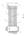
Figure 11 is the perspective view of the hard wire layout of Fig. 2 system.
Figure 12 A is the block diagram according to Point-to-Point system of the present invention.
Figure 12 B is the block diagram of point-to-point connection that has Figure 12 A of impedance matching earth grid P-channel device at this IC interior.
Figure 13 A is the one way signal transmission system on single integrated circuit and the perspective view block diagram of bidirectional signal transmission system.
Figure 13 B is the block diagram of the perspective view of four signal transmission systems on single integrated circuit.
Figure 14 A is the fixing reference voltage of prior art, the big mid point about logic high voltage level and logic low voltage level of its value.
Figure 14 B is the auxiliary reference signal, and it has identical variation as any signal.
Figure 15 A is the differential amplifier of the difference between amplified data signal and the reference signal.
Figure 15 B is the block diagram of control logic.
Figure 16 has by a kind of power save signal or is used to close the circuit diagram of single-ended signal receiver that the receiver enabling signal of supplying with receiver power supply is come the differential amplifier of gating when not in use.
Figure 17 be from read write require high-speed bus to turn to or the application that vice versa the sequential chart of signal transfer time.
Figure 18 is the block diagram of point-to-point system.
Figure 19 illustrates has signal received multiple bus system simultaneously.
Figure 20 is the block diagram with three bus systems that are used to obtain wider bandwidth.
Figure 21 explanation is used for the prior art systems of DRDRAM, and this system uses a kind of clock line with two sections.
Embodiment:
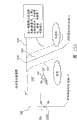
The invention provides in multiplex bus or be used for the signal transmission system and the method for high-speed communication in the point-to-point connection between multichannel VLSI equipment, and provide lower power loss with respect to the existing method that connects single-ended signal.A plurality of memory devices that this signal transmission system can be used for having multiplex bus are connected to one and are used for data, the Memory Controller of the transmitted in packets of address and control information.By using multibus, the equipment as DRAM, cross point switches, processor, wide SRAM and system controller can lump together so that obtain bandwidth greater than four GB/seconds.In fact, need all signals of computer or other digital system on this bus, to be sent out.The people that are proficient in this technology will recognize that in this computer system all need method and bus structures of this system as the equipment of CPU.
Fig. 2 A is that explanation has the block diagram of perspective view of system 200 that is coupled to the main equipment (transmitter) 205 of a plurality of slave units (receiver) 210 via bus structures (transmission line) 215 according to the present invention.As described, HRP-configured master device 205 is in order for example to comprise single-ended signal S0-S17, little skew auxiliary source synchronizing voltage and timing reference signal SSVTR and/SSVTR, 20 (20) individual signals of parallel power line (not shown) and earth connection (not shown) are sent to each slave unit 210 via transmission line 215."/" is used to represent logic NOT (NOT).As agreement was defined, signal S0-S17 can be multiplexed or non-multiplexed data-signal, control signal or address signal.Perhaps have as the clock or initialization additional signal or the additional signal that are used for by desired other purpose of agreement as the system synchronization.
As shown in Figure 3A, when each SSVTR and/during SSVTR signal triggering (upset) useful signal by main equipment 205 drivings.People will understand that slave unit 210 can comprise multipath receiver (405 among Fig. 4), and there, each receiver comprises two comparators, and one is used for this signal and SSVTR relatively, and another with this signal with/SSVTR relatively.Current demand signal binary value randomly by use have SSVTR and/XOR of SSVTR determines which comparator is coupled to output 420.Up to SSVTR and/before SSVTR changed their binary value, whether the comparator that is activated in the receiver 405 detected and changes in the signal binary value.
For bus or point-to-point on chip to chip communication, all signals are preferably in the roughly the same time and are transferred to connected another chip or a plurality of chip on this bus from identical chips, and has roughly the same load, skew and switching rate (when these signals are shifting).Similarly, preferably also be driven to other zone or other piece same area from same area or piece for these signals of inside chip, and preferably have identical load, skew and switching rate (when signal shifts) in the roughly the same time.Figure 19 that describes below and 20 explanations are used to guarantee that signal is at driven a kind of system and method for roughly the same time.
For very convenient high data transfer rates on this external bus, when SSVTR was low level (promptly/SSVTR is a high level), these bus cycles just began.When SSVTR was low level, all transmitted in packets began during this cycle, and were becoming the low level end with SSVTR, so that preset the receiver 405 of the last binary value that is used for this signal easily.This just allows the sudden transmission of even bit.When signal when being two-way because SSVTR and/transmission delay or the causes for stable of SSVTR, when this signal demand changes direction (because multiplexed characteristic of signal), need more than one null cycle so that this bus is settled out.Described below Figure 17 explanation is used for two-way timing that bus turns to and loses null cycle avoiding.
Fig. 2 B is the block diagram that explanation has the system 200 (Fig. 2 A) of the transmission line 215 that connects external impedance matched resistor 220 at two ends, and this resistor has the terminal resistance that equals to be preferably in the characteristic impedance between the 50-70 Europe.This end voltage is noted as VTT, and it is preferably about 1.8V for 2.5V operating voltage (being used for the VCC of 2.5V and the VSS of 0V).The rated voltage skew preferably is set to less than 1V, preferably less than 40% of supply voltage, and is preferably disposed on 500mv.Therefore, as shown in Figure 3A, output HIGH voltage (VOH) is 1.8V, and output LOW voltage (VOL) is 1.3V.
Fig. 3 A be explanation with respect to the auxiliary reference signal SSVTR of signal detection time and/sequential chart of SSVTR.SSVTR begins at VOL, and/SSVTR begins at VOH.In the 1st cycle, main equipment 205 comprises all in the identical time/and the low level signal of the well afoot of SSVTR is driven into VOL, and terminal resistance 220 will be moved VOH on the SSVTR.The single-ended signal of high level remains on VOH by terminal resistance.Promptly be used to detect time of logical level of input signals appropriate detection time, is after the transfer of SSVTR and/SSVTR is connected and before stabilization time, promptly when SSVTR and/SSVTR is when VIH or VIL arrive stable state.SSVTR and/SSVTR preferably has equal rise time and fall time, wherein, the cycle that is approximately each rise time and fall time any reference signal to half.
Fig. 3 B is the explanation SSVTR relevant with single-ended signal and the sequential chart of/SSVTR.Equal/SSVTR at the high voltage place when single-ended signal begins, transfer to low-voltage along with/SSVTR then.This single-ended signal remains on low-voltage then.Therefore become and equal SSVTR, then along with SSVTR transfers to high voltage.Single-ended signal remains on high voltage then, thereby becomes and equal/SSVTR.
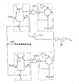
Fig. 4 is the high level schematic diagram that explanation has the single-ended signal slave unit 210 of the receiver 405 that is used for each signal line 215.Each signal receiver 405 has 410, one comparator 410a of two comparators and is used for a single-ended signal that enters " SNx " and SSVTR relatively, another comparator 410b be used for SNx with/SSVTR relatively.Two comparators 410 all have the outlet terminal that is coupled to an outlet terminal 420 selectively via switch 415.People understand the preferably absolutely dry line of this output signal (SN) (rail) signal (0V-2.5V) that is transferred to outlet terminal.
As mentioned above, SSVTR is set to VOL at first, and/SSVTR and SNx be set to VOH at first.SN is set to an absolutely dry line high output voltage at first.Therefore, this comparator 410a amplification deducts the high voltage SNx of low-voltage SSVTR, thereby high output signal is provided.Comparator 410b amplification deducts the high voltage SNx of high voltage/SSVTR, thereby the output signal of the unknown of a noise amplification is provided.Switch 415 is selected by XOR (XOR) gate 425 Be Controlled.Especially, XOR gate 425a compares an absolutely dry line SSVTR signal (VT) that is exaggerated with output signal SN, and produces a control signal that is used for control switch 415a.XOR gate 425b with absolutely dry line/SSVTR (/VT) with output signal SN relatively, and produce a control signal that is used for control switch 415b.In this initial condition, having only SSVTR and corresponding VT is low level, thereby makes XOR 425a drive the switch 415a that closes.Therefore, comparator 410a output (high level) arrives outlet terminal 420.XOR 425 drives the switch 415b that opens, thereby prevents to enter useless output signal from comparator 410b.At this moment, receiver is stable.
According to example illustrated in Fig. 3 B, this single-ended signal SNx transfers to low-voltage.As from start to finish, SSVTR and/SSVTR transfers to another kind of polarity on the contrary.Therefore, SSVTR and/SSVTR once reach between them predetermined difference (being preferably 250mV) VT and/the VT transfer.Similarly, SSVTR and SNx one transfer to the predetermined difference (being preferably 250mV) between them, and comparator 410a also shifts (to low output voltage).People understand from external signal SNx to the path that produces output signal SN and be used for absolutely dry line signal VT and/ path that VT generates, each path comprises a comparator 410 or 435 and two reversers 430 or 440.Therefore, each XOR 425 will be according to receiving new input signal by comparator 410 and 435 speed relatively.In this example, the example of the sequential chart by Fig. 3 B is apparent, SSVTR with/SSVTR will reach a predetermined difference in the identical time, thereby SSVTR reaches identical predetermined difference with SNx.Therefore, XOR 425a will continue to receive differential input, thereby keep a pent switch 415a, and the low output voltage that makes comparator 410a is by reaching outlet terminal 420.At this moment, receiver still makes stable.
Still according to the example of Fig. 3 B, single-ended signal SNx does not shift.As from start to finish, SSVTR and/SSVTR shifts with respect to another kind of polarity mutually.Therefore, the current comparator 410a that is activated continues to drive a low output voltage.When SSVTR and/when SSVTR arrives with respect to the predetermined difference of another kind of polarity, just before SSVTR arrives identical voltage as SNx the possibility of a kind of unsettled condition of this output signal (thereby avoid), XOR425a will close, and XOR 425b will connect.Begin to rise from this time/SSVTR, comparator 410b can drive a low output voltage.At this moment, receiver remains stable.
Each receiver 405 can easily detect and amplify the very little signal of about 100-250mV.If shift in single-ended signal SNx, so, output signal SN has the new level opposite with its former signal level.Because SSVTR (or/SSVTR) shift, so identical comparator 410 still is coupled to signal output part with single-ended signal.If single-ended signal SNx does not shift, so, this signal output SN does not change, the comparator 410 that begins to be coupled in transfer SSVTR and/the SSVTR receiver amplified their new binary condition (VT﹠amp; / VT) afterwards from this output by decoupling, and other comparator 410 with opposite/SSVTR (or SSVTR) is coupled so that this signal output is provided.Therefore old output level is resumed.
Do not use XOR receiver 405 can be implemented yet.This can by use in initial period SSVTR and/known polarity and the initial high level of all single-ended signals of SSVTR realize.This SSVTR and/SSVTR shifts in each in cycle.Therefore, in each cycle their polarity can by check in certain synchro system system clock and even number in the clock cycle delimiting period begin (promptly this even number in the clock cycle SSVTR be low level, and/SSVTR is a high level) come to determine.Then, have only this output signal to be monitored so that whether the change state makes comparator 410 coupling and decouplings in each cycle according to output signal SN.If output signal SN changes state, the comparator that is coupled is so just let matters aside.If this output signal SN does not change, the comparator that is coupled so is just by decoupling, and other comparator is coupled or the like.
Certain system that the present invention is specialized can make all signals be connected so that reduce source of resistance, can make all signals produce voltage and in fact differentiated noise conditions aspect immunity to interference, and with other as RAMBUS, HSTL or the comparison of GTL single-ended signal transmission technology can reduce variation.0.5 the little skew that is implemented in this exemplary embodiment allows to be used for to have the very high signal rate of much lower power consumption when with other existing single-ended signal transmission technology comparison.In addition, people understand, each receiver 405 amplifies this single-ended signal SNx and do not need conventional clock or other timing signal during this signal shifts, SSVTR, the distortion VT that/SSVTR and they are exaggerated and/VT except.
Fig. 5 is that the explanation signal of communication is crossed over the flow chart of transmission line 215 to the method 500 of receiver 405 from main equipment 205.Method 500 is from main equipment 205, and SSVTR is set to VOL in step 505, and all single-ended signals (/SSVTR and SNx) are set to VOH, and in step 510 all single-ended reception outputs (SN) is set to absolutely dry line high level.Receiver 405 makes comparator 410a coupling in step 515, this comparator is sent to the single-ended signal SNx comparison of the output 420 of this receiver 405 with SSVTR and each.Receiver 405 in step 517 makes under all signal stabilizations on this transmission line.Step 505-517 is called system initialization.
Fig. 6 A is a kind of schematic diagram of connecting and disconnect slowly the main equipment 205 that is used for single-ended signal slowly of explanation, and this main equipment is called transmitter 600 in first embodiment.Transmitter 600 comprises a NMOS pull-down device 605 that is coupled to the transmission line 610 that is used for accurately making output offset be suitable for 500mv below VT.NMOS pull-down device 605 comprises a pull-down NMOS transistor T 1, and its source electrode is coupled to transmission line 610, and its drain electrode is coupled to ground, and its grid is coupled to and departs from control circuit 620.Depart from control circuit 620 and comprise a CMOS reverser, this reverser comprises two transistor Ts 2 and the T3 that is coupling between two resistor R 1 and the R2.The input that is connected to the CMOS reverser is coupled to signal controlling equipment 625.For example, for produce SSVTR and/SSVTR, this signal controlling equipment 625 can be an oscillator.People understand that drop-down quantity can use a resistor (not shown) and a serial pin (not shown) to regulate so that be that any operation or equipment change are provided with correct variation during initialization.The similar approach that the use feedback technique that has illustrated in " CMOS subnanosecond True (very)-ECL output buffer " being entitled as of delivering people such as solid-state circuit periodical the 25th volume (I) 150-154 page or leaf (1990.2) Hans Schumacher is controlled also can be used.The parallel terminal that (when by R1 and R2 control) is kept the 20ma electric current and had a 50ohm at the two ends of this transmission line 610 will produce 500mv under all conditions and be offset.In order to have at a slow speed lifting time at output and to make reflection, signal coupling and terminal network switch noise reduce to minimum, depart from control circuit 620 control pull-down transistor T1 so that switch on and off at a slow speed.In the transfer time for 500mv is under the situation of 0.8ns (millisecond), and best transition speed is 1.6ns/volt.
For a signal that shifts equably as the slope, the best transition speed of signal is that two reversers postpone and four times of an XOR delay summation in a kind of given technology.In having 0.25 μ CMOS technology of 2.5V operating voltage, it is 50 psecs that reverser postpones, and XOR postpones to be approximately 120 psecs.Therefore, best transition speed is approximately 880 psecs.For the signal that is transmitted more than the speed of 600MHz, this conversion of signals speed is preferably less than 110% of this signal rate.If this signal reach than this change-over time Zao 3/4 it final value 75%, just fast a little for the best transition speed of exponential signal so.This differential wave is preferably crossed over the centre of shifting through overvoltage.Through the place, 3/4 path that overvoltage shifts, this signal has the difference of about 250mv approximately, and this difference can promptly be transformed to a big shifted signal.When receiving the single-ended signal of non-transfer, amplify and prevent that stop signal is coupled to this receiver output for fear of noise, the transfer time 75% between (voltage transfer path 3/4) and the final signal value is more preferably greater than two reversers postpone and this XOR postpones summation.This switching rate can be carried out soon as handling the noise that amplifies, so that arrive the output of this comparator 410, the output of comparator is coupled to output 420.In other words, when receiving the signal of a non-transfer, the state that switch 415 amplifies according to noise before this comparator output change state is with transition status.The output of the current comparator that is coupled 410 is near a kind of uncertain (noise is exaggerated) state.Switch 415 must transition status before uncertain output becomes effectively.People understand that also equipment does not match, and manufacturing tolerance and signal reflex will influence speed, and the output of comparator 410 reaches uncertain state with such speed.Along with the improvement of this technology, gate delay, faster switching rate and faster signal rate can realize.
Fig. 6 B is explanation has adjustable conversion of signals speed and the main equipment 205 that departs between signal a schematic diagram, is called transmitter 650 in the exemplary embodiment of another kind.Transmitter 650 comprises that one is coupled to transmission line 610 so that accurately make output offset satisfy the NMOS pull-down device 655 of the requirement of 500mv below VTT.This NMOS pull-down device 655 comprises a kind of pull-down NMOS transistor 660 that is connected in parallel, and each transistor has its source electrode that is coupled to transmission line 610, is coupled to its drain electrode on ground, and is coupled to its grid that departs from control circuit.Depart from control circuit 655 and comprise a CMOS reverser, it comprises two transistor T 2 and the T3 that are coupling between two groups of resistors that are connected in parallel 670 and 675.The input that is connected to the CMOS reverser is coupled to signal controlling equipment 625.This transistor group 670 and 675 is regulated lifting time.People understand that lifting time is preferably symmetrical as far as possible so that have all signals of mid point cross-over connection and read all signals so that these signal Synchronization are occurred by differential receiver.Realize symmetry and switching rate is set and output offset can be finished by a register (not shown) is set during by blowout (not shown) or the initialization at circuit board during the test phase.
Signal transfer time can be higher a little than signal rate.In the big bus of some load capacity, skew can increase so that transmission loss is aroused attention, but still provides 500mv so that read easily for receiver 210.People also understand according to technology, load, and receiver acquisition and resolution postpone to make various switching rates, and index transfer time and variation become possibility.Even when bursting, reach the situation of 90-95% of their final value in transfer time following transfer time may be a little than signal rate height.Also can before regulating, use drop-down size of NMOS and resistor in this, test single-ended signal and SSVTR and/regulate transfer time during departing between the SSVTR, use as the laser blowout or the well-known technology of register code be set so that obtain in the signal waveform shape shown in Figure 10.As shown in figure 10, SSVTR and/SSVTR shift before all single-ended signal SNx should be overlapped or less than 50psec (psec).This departing from can be regulated after the test in this scope.
The another kind of embodiment of each signal receiver 405 of Fig. 7 A-7D key diagram 4.People understand that the comparator 410 of receiver 405 must be worked during each cycle, thereby require little catching with resolution to postpone, and do not have input current to be taken into and do not have electric current to annotate to get back in the signal line.Public differential amplifier satisfies all these requirements.With reference to Fig. 7 A, receiver 210 uses 702, one differential amplifier 702a of double differential amplifiers to be used for signal SNx and SSVTR relatively, and another differential amplifier 702b is used for signal SNx and/SSVTR comparison.For the purpose of complete, the brief explanation of a differential amplifier 702 is provided.This differential amplifier 702 is activated all the time.According to the channel size, when SSVTR voltage was higher than SNx voltage, more multiple current was driven and strides across PMOS transistor T 10, thereby output voltage is drawn high (near VCC or 2.5V) at node 707.When SSVTR voltage during less than SNx voltage, more multiple current is inhaled into and strides across nmos pass transistor T11, thereby output voltage is dragged down (near VSS or 0V) at node 707.This differential amplifier is transformed into a big skew (0V or 2.5V) voltage with 0.5V (little skew) input.
The output of differential amplifier is exaggerated, and by reverser 704 conversions, is connected node 708 together through cmos transmission gate 706.This transmission gate 706 is worked selectively, it depend on have respectively SSVTR or/SSVTR, promptly VT or/VT by the state that is exaggerated with front signal (SN) of XOR.Reaching their SN of logic level separately, VT and/be not used in that designed XOR-R is stable under the low-frequency disturbance situation that little timing changes between the VT.
At the various embodiment shown in Fig. 7 A a kind of differential amplifier that is activated all the time is described, this amplifier has only one to be activated the transmission gate that is used for skinny device number and more speed selectively as another kind of embodiment 700.Fig. 7 B illustrates differential amplifier and the transmission gate that an energy is started simultaneously or can not be started simultaneously as a kind of embodiment 720.As another kind of embodiment 740, Fig. 7 C illustrates a kind of differential amplifier, and this amplifier starts by being used for lower powered identical XOR, and the result is energy quick closedown transmission gate during the transfer of XOR output, and can the slow start transmission gate after this XOR is stable.As another kind of embodiment 760, Fig. 7 D illustrates a kind of P-raceway groove differential amplifier with the 1.2V end voltage that is used for low power applications.When this receiver or this equipment do not have when selected, or this equipment is in very in the battery saving mode, and in order to reduce power, all differential amplifier doors can be closed.This differential amplifier can be closed by disconnecting transistor T 11.
By using 1.2V terminal and the receiver 405 shown in Fig. 7 D, power consumption can also reduce 33% again.In other words, variation will drop to 0.7V from 1.2V, and the result is for suitable surplus and the low power consumption of portable system permission from the ground connection reflection.This operating frequency can be similar with negligible amounts equipment on the bus, and this frequency is with general than the portable set of form factor.This transmitter 205 can also be being connected in parallel of drop-down T1 of a kind of NMOS or NMOS drop-down 660.Except that this differential amplifier 702 becomes a kind of mirror image, the work of receiver is similarly, owing to increased the equipment size of P-raceway groove, thereby this gate capacity approximately increases by two times when signal is entering the P-ditch sect that is used for similar characteristics.The configuration that little skew differential wave is transformed into fast other differential amplifier of big skew differential wave can be used by alternately, with the differential amplifier shown in substituting.The people who is proficient in this technology will recognize that another kind of embodiment can use two different VTT, a signal that equals 1.8v that is used to have the 500mv skew, and another is used to have the vibration reference signal that equals 1.7V of 300mv skew.All signals are transferred at one time, and have similar switching rate.Identical transmitter and receiver is to controlling multichannel VTT system.
The DC bias point of each differential amplifier in receiver 405 is disposed like this, when two little offset voltages (the single-ended signal SNx of the differential amplifier that is activated and SSVTR or/make receiver 405 output voltages be lower than half of VCC during SSVTR) near VIH, and when two little offset voltages during near VIL this output voltage be higher than half of VCC.SNx does not change state when this single-ended signal, and the SSVTR of the differential amplifier that is activated or/SSVTR before this amplifier decoupling during just near this differential wave this bias voltage consider the suitable surplus of output signal SN and keep this output signal.
Because it is receiver 405 is worked during the signal that is used for a little skew single-ended signal shifts, no longer suitable in the former signal transmission technology after this signal level arrives VIH/VIL or VREF from foundation and the notion of retention time of certain time that is prescribed.There is not VREF (reference voltage) to be used for comparing with this signal voltage yet.By near the timing that cancellation is used to set up and keeps needed timing and must be able to realize the voltage margin that is used for reading VREF, operating frequency is along with the reduction of power consumption will increase widely.In addition, all receivers 405 are by self-timing, and do not need a kind of global clock, thereby allow receiver 405 to be conditioned individually, so that eliminate card or the assembly level transmissions departs from.
Fig. 8 A and 8B are the circuit details of the comparator 435 of key diagram 4.Each comparator 435 comprises the differential amplifier 802 (Fig. 8 A) of the differential amplifier 702 of similar Fig. 7 A or the multistage reverser 804 (Fig. 8 A) or 854 (Fig. 8 B) of 852 (Fig. 8 B) and serial.Comparator 802 and 852 (VT1, VT2, VT3 ,/VT1 ,/VT2 and/absolutely dry line signal VT3) is transferred to the XOR 425 (Fig. 4) of all single-ended receivers.According to test to the signal speed of the speed that is substantially equal to receiver 405 output signal SN generation passes, VT1, the selection of VT2 or VT3 is determined.
Fig. 9 is that explanation has single adjustable delay so that the elimination schematic diagram that departs from and little skew is converted to the receiver 405 of big skew by comparator 410 during the transmission.For operating frequency or variation are adjusted to optkmal characteristics, each receiver 405 have one be used for the register 905 of stored data so as to make three VT1 and/VT1, VT2 and/VT2, or VT3 and/among the VT3 one can be transported to XOR 425 (Fig. 4).
Figure 11 is the perspective view of the hard wire layout of a main equipment that is combined 1100 that is used for two-way signaling communication.Main equipment 1100 comprises the receiver 405 that is coupling in together and returns transmitter 1105.Especially, each received single-ended signal is coupled to a respective receiver 405 as signal S0, as receiver S0 and be coupled to a corresponding transmitter 1105, as transmitter T0.Preferably, all single-ended signal SNx can with SSVTR and/the SSVTR reference signal combines.But the people that are versed in this technology recognize, for given frequency of operation SSVTR and/SSVTR load and signal is uneven can reduce the number that can be combined in signal Snx together.As shown in figure 11, this layout is done so that make at SSVTR, the electric capacity when/SSVTR and all single-ended signals, and resistance and inductance keep balance.In addition because SSVTR and/SSVTR is sent to all receivers 405, therefore for SSVTR and/total load of SSVTR must reduce to minimum.
Have the physics packing of low-down power consumption and sealing by use, this bus can be done shortly as far as possible, thereby equally also allows to be used for short propagation time and high data rate.Shown in Fig. 2 B, the control group transmission line of resistance terminating can be with 1Ghz (1 nanosecond period) signal rate work.The characteristic of this transmission line is subjected to the influence of the load that the integrated circuit by the DRAM on being installed in this bus causes consumingly.These integrated circuits are attached to lumped capacity on this circuit, thereby not only reduce the impedance of this circuit but also reduce transmission speed.In the environment that is loaded, this bus impedance may be approximately 25 ohm, and propagation velocity is approximately 7.5 centimetres/nanosecond.Must not should be noted that simultaneously from two these buses of device drives.Therefore for less than 12 centimetres bus,, must have make this total line stabilization a null cycle (for example 2 nanoseconds) in order to be transformed into another driver from a driver.For long bus, perhaps need be greater than one-period, so that before a new transmitter can drive this signal, make under this signal stabilization.Different with RAMBUS, the length of this bus reduces operating frequency with burst mode from identical equipment really.
Figure 12 A is the perspective view block diagram of a Point-to-Point system of explanation, and this system comprises a two-way main equipment 1205 that is coupled to a two-way slave unit 1210 via transmission line 1215.Transmission line 1215 comprises upper signal SNx circuit 1220, bottom signal SNx circuit 1225 and SSVTR and/SSVTR circuit 1230.As Figure 12 B was illustrated, this figure was the Point-to-Point system 1200 of the terminating resistance 1235 that uses earth grid P-channel device is equipped with in an explanation in inside a perspective view block diagram.So cancellation to the needs in space so that connect non-essential resistance and reduce cost.People recognize that this terminating resistance 1235 can use internal resistance to replace earth grid P-channel device to realize.Two terminals with suitable characteristic impedance are preferably used in the two-way signaling on the bus.Because the inside chip piece is the most approaching physically, therefore do not need impedance matching resistance.Use little drawing device just enough.Similarly, when inside chip be connected physically near the time, impedance matching resistance can substitute so that reduce cost and power with little drawing device, and keeps identical switching rate.
People will recognize that for picture SLRAM, DDR SDRAM or the such equipment of DDR SRAM require multibus, there, are transmitted and receive to signal Synchronization.Figure 13 A is the perspective view block diagram that the unidirectional and bilateral system 1300 of a kind of combination that is used for the SLDRAM on a single integrated circuit is described.System 1300 comprises a main equipment 1305 (for example SLDRAM) that is coupled to slave unit 1310 via transmission line 1315.Main equipment 1305 sends address and control signal via address and control circuit 1320 and 1325, stride across data circuit 1330 and 1335 transmission/reception data-signals, SSVTR and/send on the SSVTR circuit 1,340 first group of SSVTR and/the SSVTR reference signal (be SSVTR0 and/SSVTR0) so that check this address and control signal, then with second group of SSVTR and/the SSVTR reference signal (be SSVTR1 and/SSVTR1) send to slave unit 1310.The address of this system 1300 and control section management are only by slave unit 1310 needed one way signals.The data division of this system 1310 is two-way, this two-way based on this control signal whether stipulated one read (READ) or write (WRITE) operation.
For a SLDRAM, 40 bits command and address are sent out with the packets of information of four 10 bit words.Can be called system's differential clock SSVTR0 and/SSVTR0 is operated in 500Mhz.Phase-locked loop (not shown) be used for the locked clock frequency and be used for the timing of various inner purposes and drive on two edges of 1Ghz data rate SSVTR1 and/the data output of SSVTR1.All high-frequency signal terminating are at two ends of the bus of the characteristic impedance with them.Terminate load on the controller end of memory can comprise non-essential resistance, and internal resistance or inner earth grid P-channel device are because the controller of this memory main equipment and fixing normally.Because the number of parts (SLDRAM) 1310 (working as slave unit) is variable, therefore at these parts 1310 best terminating non-essential resistances of end of transmission line.18 bit BDB Bi-directional Data Bus 1330 and 1335 are operated in same frequency as being used for synchronous system clock, and send data from single SLDRAM with eight 18 bit words in four clock cycle (8 nanosecond) or with 2.25 GB/second speed.Note by increasing empty door and circuit so as to seem to be similar to SSVTR1 and/SSVTR1 makes the load balance on SSVTR0 and the/SSVTR0.Because load is similarly and allows similar surplus for all signals, therefore this load balance forms switching rate.
When the bandwidth of having relatively high expectations, shown in Figure 13 B, system 1350 can use four buses.Under controller 1305 situations that single memory is arranged, use the segregated channel of two SLDRAM 1310.This configuration allows the peak-data bandwidth of 4.5 GB/seconds.Though this system 1350 do not require synchronised clock and be used for transmitter 1305 or receiver 1310, this system 1350 can use synchronised clock so that be easy to test and effectively special time and frequency sending data under the situation of the existing agreement of synchronous DRAM and SRAM.For reduce noise and system power do not use be used for synchronous high-frequency clock and be to use one at a slow speed on the sheet of clock multiplier or an inner annular oscillator may be desirable so that send data at high frequency.People recognize that the people that are skillful in this technology can rely on instruction of the present invention to realize various sizes, synchronous or asynchronous and wide bandwidth system.
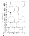
Five notions of the input and output circuit 210 of further key-drawing 4 will be provided below.
First notion relates to and has the auxiliary reference signal.Shown in Figure 14 A, prior art systems uses a kind of its fixing value greatly in the middle of logic high voltage level (VOH) and logic low.VREF generator (not shown) has the DC skew from the power source change that is used to produce it usually, and this variation is illustrated with " VREFH " and " VREFL " form.Because transient change in supply voltage, ground connection reflection (bounce), and with the electric capacity and the inductance of adjacent signals coupling, also have some AC noises.The differential offset that is sent to employed comparator in the receiver of prior art illustrates by arrow.Should be noted that error situation differential wave in the prior art will be the 1/3-1/4 of the total voltage of this signal.
As shown in Figure 14B, system and method for the present invention use as any signal (for example data or control) have identical variation auxiliary reference SSVTR and/SSVTR.In a kind of preferential embodiment, this variation is the 500mv of the logic low-voltage (VOL) of logic high voltage (VOH) with 1.8v and 1.3v.People will recognize, in the operating period of sort signal transmission system, each moment this auxiliary reference voltage mean value greatly about the mid point of VOH and VOL.This signal has identical transfer time and variation with the auxiliary reference signal, and (is used for the identical device of inside chip or is used for the identical general address of inside chip) from the identical source that is sent to this receiver in the identical time.In other words, this auxiliary reference signal seems just as any other signal.But when other signal demand sent at every turn, this auxiliary reference signal just was triggered.Because this auxiliary reference signal uses power supply and the earth simultaneously, thereby all noises are common mode.Therefore, the VREF of needed signal bias in the prior art changes (VREFH and VREFL) does not need in the system and method for the present invention.Because the binary properties of digital data transmission, in the beginning of this reference transfer with finish to have the polarity opposite all the time with this signal.Therefore, a current reference (signal) has the total drift of the about 500mv that produces in certain time, earlier reads this signal voltage thereby can make comparator than 1/3 or 1/4 the prior art systems that only has the resultant signal skew.This signal and reference signal can be that half of prior art required transfer time is so that obtain identical differential wave transfer time during signal changes.The people that are skillful in this technology recognize, for optkmal characteristics, VOH and VOL should be arranged on and be lower than power supply hundreds of millivolt and be higher than between the earth hundreds of millivolt Anywhere, and the potential difference between power supply and the earth is 500 millivolts.Especially in inside chip communication, if this device mismatch is reduced and the reflection of signal is very little or do not have, this potential difference can further be reduced to 200mv-300mv so.
Second notion relates to and has the dual comparator that is used for each entering signal.Refer again to Fig. 4, because this signal and two auxiliary reference signals are relatively, so each receiver 210 has two comparators.One is with signal SNx and SSVTR relatively, and another with signal SNx with/SSVTR relatively.Shift beginning bursting, the comparator that has full differential wave at its input is coupled to receiver 210 outputs, and the comparator that another does not have a differential wave from receiver 210 outputs by decoupling.This finishes by initialization.If signal SNx and the reference signal that is coupled shift, when an amplifier amplified this signal apace and this output is driven into inverse state, this comparator was just read this signal apace so.If having to shift (promptly having only reference signal to shift), signal SNx is not sent to the differential input of the comparator that begins to be coupled in the reference signal transfer so through reducing steadily transfer time, at last up to there not being signal to provide.Being sent in reference signal transfer beginning will be increased by the differential input process of the comparator of decoupling transfer time steadily, is provided up to a full differential wave.Originally the comparator that does not have differential wave that was coupled when shift finishing is by decoupling, and is coupled by the comparator with full differential wave of decoupling originally when this transfers end.The present invention uses two comparators to read a signal.In addition, in the beginning of each possible effective transfer, the binary properties of digital signal guarantees to have a full signal skew in a comparator.
The 3rd notion relates to initialization.Owing to once have only a comparator to be coupled to the receiver output, therefore importantly the comparator that begins to be coupled to receiver 210 outputs and have complete differential input signal bursting will be arranged for suitable operation.Therefore, all signal S0x-SNx are initialized to logic high VOH.By closing all devices, SSVTR is initialized as VOL, general/SSVTR is initialized as VOH, and this signal is connected to terminal resistance or have the grid that is switched on and be connected to VTT (VTT is 1.8v) source electrode on draw the P-raceway groove, thereby reduce power consumption.Receiver 210 output that is used for S0-SN is pre-charged to the VCC of the P-channel device of using Figure 16 to high level and is coupled to receiver 210 outputs so that guarantee the comparator that control logic (explaining below) will have a full differential wave.
The 4th notion relates to signal and changes discriminating.The people that are proficient in this technology are well-known, and a kind of characteristic of differential amplifier is intended to a small voltage difference is amplified to big voltage difference.Size and the gain of transistorized matching voltage according to equipment are generally 3-5 doubly.The reverser that is positioned later at this differential amplifier provides additional gain so that select almost to obtain full migration according to equipment size.For obtaining full migration, the speed of this differential amplifier and reverser depends in the useful differential wave of its input.Shown in Figure 15 A, a differential amplifier (with a reverser) 1501 can both amplify the transfer among SNx and the SSVTR1500 soon.But, when SNx does not shift, the signal that is sent to this differential amplifier will be reduced to appropriate noise and slowly many speed (on mismatch and noise basis).Transfer signal SN ' (output of differential amplifier and reverser) is represented as chain-dotted line 1503.The zone 1502 that belongs to the left side of transfer signal SN ' 1503 is noted as " Change (variation) ".The zone that belongs to the right of transfer signal SN ' 1503 is noted as " No Change (not changing) " as mentioned above when signal does not shift, and amplifier 1501 is reduced to rational noise with noise, and it is represented as a uncertain region 1506.The time interval before this amplifier reaches this uncertain region 1506 is represented as temporary transient interstitial area 1504.The present invention utilizes this time slot, by starting following illustrated control logic so that the signal in will changing is delivered to the receiver output, and prevents from the neutral signal in transmitting.By selecting suitable equipment size and transfer time, this time slot can be formed is enough to make control logic to be worked in this wise, make that " signal change (signal variation) " passed through, and " no signal change (no signal variation) " and consequent uncertain voltage signal must not pass through.People will recognize, as long as certain uncertain voltage level is less than the logic threshold of following in thereafter XOR gate, some uncertain voltage level can pass through so.Other comparator can recover this voltage level apace then.People will recognize further that this time slot depends on signal bias, and reference signal transfer time, operation does not match and signal reflex etc.
The 5th notion relates to control logic.With reference to Figure 15 B, this control logic circuit 1550 is coupled to receiver output 1560 with suitable comparator 1555 and with by using SSVTR, and the timing that differential amplifier produced of the output of/SSVTR and current receiver 1553 is the basis.With reference to Fig. 4, before the beginning of bursting, by input signal S0x-SNx is initialised to VOH, to be initialised to VOH with reference to/SSVTR, to be initialised to VOL with reference to SSVTR, and receiver output signal S0-SN will be initialised to VCC, suitable comparator 410 will be coupled to receiver output 420.For a transfer signal, because this control logic XOR1565 selects suitable reference signal that is exaggerated and signal receiver output, so control logic 1550 does not change.Because the SSVTR reference signal that is exaggerated shifts with SNx and the SSVTR reference that is used to be exaggerated all is identical with being used for the delay path of SNx to XOR1565, so XOR 1565 does not change.On the other hand, if the signal that enters does not shift, the so former comparator 1555 that is coupled is by decoupling, and another does not have comparator 1555 of coupling to be coupled now.If desired, this signal receiver output does not change, and is driven energetically so that recover output level by the comparator 1555 that is coupled.As explained above, this control logic be designed in case appear at signal change 1502 and signal do not change during the time slot 1504 between 1506.
This control logic realizes by each comparator being used partly an independent XOR, and this comparator is used for regulating timesharing preferably at a high speed, and is used to improve surplus and adjusting and departs from and do not match.Also should be equipped with all from the SSVTR of all signal receivers of using a bus channel and/SSVTR regularly and the comparator of the receiver of control signal output decoupling, so that control logic appears in the timesharing during this time slot, thereby reduce the number of devices that receives machine.Before the next one shifts beginning, when must being connected to receiver output, suitable comparator will reduce bandwidth of operation.
When all these elements are combined in a time-out, whole signal transmission system will with all signal S0x-SNx and with VOH begin /SSVTR works the SSVTR that all signal receivers outputs are precharged to VCC and begin with VOL together.This signal burst shift beginning along with the auxiliary reference signal before all thereon (SNx and SSVTR) comparator with differential wave be coupled to the receiver output.When signal shifted, this control logic allowed this signal that this output is driven into opposite voltage rail.When signal did not shift, this control logic made the signal decoupling from current comparator to another comparator so that keep and/or the output of recovery receiver.Thereby next the transfer with the pipeline conveying allows next transfer so that continue overlapping transfer with control logic up to this control logic delay qualification bandwidth or the time interval.
As shown in figure 16, the single-ended signal receiver has by a kind of power saving (parts) of the signal of cutting out the power supply of supplying with this receiver or differential amplifier that receiver carries out gate of starting when not in use.With Fig. 7 A relatively, power saving (parts) or the NAND door 1610 of receiver of this reverser by being coupled to enabling signal is replaced.In addition, pull-up resistor 1615 has been coupled to node 708 in its drain electrode, is coupled to VCC at its source electrode, is coupled to the power saving of enabling signal or receiver so that SN is pre-charged to VCC at its grid.Also obtaining correct polarity at differential amplifier back NAND door 1615 for SN bursts the cycle so that start.Along with moving high level by terminal resistance or drawing device on SNx on this signal line, initial conditions plans SNx is preset to high level, and SSVTR is preset to low level, and general/SSVTR is preset to high level.Remaining receiver operation is illustrated.During powering up or XOR-when R output did not reach stable level, if necessary, the P-channel device on the common node of this transmission gate output was pre-charged to high level with node 708 apace.
Equipment by using low-down power consumption and the physics of sealing packing, this bus can be made into short as far as possible, thereby similarly allows short propagation time and high data rate.As shown in figure 12, terminating control group transmission line can be operated in 1GHz (1 nanosecond) or higher signal rate.The characteristic of this transmission line is subjected to the influence of the load that the integrated circuit by the RAM on being installed in this bus causes consumingly.These integrated circuits are attached to lumped capacity on this circuit, thereby reduce the impedance of this circuit, and reduce transmission rate.In the environment that is loaded, this bus impedance may be approximately 25 ohm, and propagation velocity is approximately 7.5 centimetres/nanosecond.As described in Figure 17, a kind of require from read write or application that the high-speed bus that vice versa comes and goes, it approximately is the 25-30% (half of this cycle time) of this signal rate that this signal is selected as transfer time.This driver is closed so that this signal is settled out with the signal rate of about 25-30%.People will recognize that the reverse next cycle of signal or data direction can be performed under the prerequisite of not losing bus efficiency, and on this bus, equipment is closer to each other, and bus stabilization time is less than half signal rate.
Figure 18 illustrates a point-to-point perspective view.By using earth grid P-channel device terminating resistance to be combined, just can constitute the high-performance Point-to-Point system as Figure 13 B in inside.Just can cancel the needs in space so that connection non-essential resistance and reducing cost by terminating resistance being combined in inside.Also might signal line discharged into desired electric current in the desirable voltage so that reduce at the door of transmitter one side conversion P-channel device.CPU and Memory Controller have P-raceway groove terminal equipment, and when their door was in earthing potential, the size of these terminal equipments can selectedly equal the characteristic impedance of this circuit.The door of P-channel device uses a kind of signal, and this signal is the complementary signal that can make receiver end and the terminal idle receiver of transmitter.When this receiver is predisposed to high level, and before the beginning of bursting on this bus, this conversion can be implemented.Internal resistance also can be used for substituting earth grid P-channel device.By using as at the illustrated multibus of next joint, CPU can reduce to 32 (36) from 64 (72) to the controller bus width of memory, and perhaps wide bandwidth can increase widely.The high-speed cache of CPU reserve connects and also can quicken, and the number of leads on CPU can reduce, and PBSRAM can change to X18 from X36, thereby reduces die size and reduce cost.
Figure 19 illustrate a kind of have be used for the picture SLDRAM, the system 1900 of the multibus of the equipment that DDR SDRAM or DDRSRAM are such, wherein signal is received synchronously.This system clock bus 1920, and finishes at this Memory Controller 1905 from clock source 1915 at the end on the opposite of Memory Controller 1905, and this Memory Controller 1905 is connected to all devices 1910 that its data output is connected to bus 1920.Be added in load on this clock signal and loading data output and SSVTR1 and/SSVTR1 is with reference to coupling.People will understand that this clock can make differential (best) or single-ended will depend on clock frequency and system requirements.The skew of this clock voltage may be similar to SSVTR and/SSVTR is so that have a similar receiver.For identical delay will be arranged, the tracking length of this clock bus 1920 will with SSVTR1 and/the tracking length of SSVTR1 reference signal is complementary.This clock source 1915 is introduced SSVTR1 at different time from DDRDRAM, / SSVTR1 and data, this depends on their positions on bus 1920, makes data like this, SSVTR1 arrives controller 1905 with/SSVTR1 in the approximately identical time, and no matter which DDRDRAM is driving these data.If need synchronously at controller 1905, each DDRDRAM can randomly use a DDL (delay lock loop) so that this clock 1915 is reduced to data delay so.In order to reduce the additional lead in the clock system that transfer of data can be concluded, DDL can be used for being created in the receiver end and have identical timing and voltage characteristic but opposite polarity/SSVTR1.This DDL (comprises controller 1905 and DDRDRAM1910) in all parts should reproduce this clock.This controller it should be noted that data and SSVTR1 reference signal are expected the cycle that arrives therein.After a write cycle time started by address and command signal, DDRDRAM ought to know the cycle that data will arrive of importing therein.When/SSVTR signal is required by particular component, DDL gating should/the SSVTR1 signal.Address and order circuit can with SSVTR0 and/SSVTR0 combination.This address and control bus uniaxially are from Memory Controller 1905 to DDRDRAM1910 transferring input signals.10 bits command and address are admitted to one 2 bits command and one 8 bit addresses form.2 bits command by use SSVTR0 and/in the signal on two edges of SSVTR0 /CE and/RAS and being used for/CAS and/other signal of WE is formed.8 bit addresses at two edges provide 16 bits nearly and/CE and/ row address that RAS occurs together or nearly 16 bits and be used for the read cycle /CE and/ row and block address that CAS occurs together.Write cycle time uses 16 bits to have/CE ,/CAS and/row and the block address of WE realize.SSVTR0 and/SSVTR0 can be the distortion of this system clock (differential), and is operated in the frequency of system clocks identical or many times.As previous the explanation, DDL can be used for being locked in the frequency that is used for various inner purposes in the Memory Controller 1905, so that should order and address signal in the read request drive, and drives the input data be used for write request, SSVTR1 and/SSVTR1.
Use be used for data inputs (SSVTR1 and/SSVTR1) and be used for address and control (SSVTR0 and/SSVTR0) different reference signals generals further transmit the present invention and RAMBUS signal to distinguish and come.In RAMBUS, all signals that enter among the RDRAM are read out according to single clock, and thus, control signal and address signal are in the different channels that is different from data-signal in the present invention.This just can be different from the different frequency operation control and the address channel of data channel.All unidirectional high-frequency signals (address and control signal) are in their characteristic impedance of terminal bus terminating away from this controller 1905.Because controller 1905 main equipment normally, and fix, thus all two-way signalings (data-signal) in the terminal terminating of controller an outside or inner resistance, or the earth grid P-channel device of an inside of terminating.People will understand, in order to reduce power, and, during data write cycle, this terminal P-channel device can be closed.Terminal in this controller one side is chosen wantonly, and can be a high resistance that is approximately 10 * this characteristic impedance.Because memory member is the number of slave unit is variable, therefore in the most handy non-essential resistance terminating of this depositing element of end of this transmission line.When system clock is used for when synchronous, this 18 bit BDB Bi-directional Data Bus preferably is operated in identical frequency, and is preferably in 2 clock cycle (4 nanosecond) or send data with 4 18 bit words from single DDRDRAM 2.25 GB/seconds.Note by increase Buddhism and circuit make SSVTR0 and/ load maintenance balance on the SSVTR0 so as to look to SSVTR1 with/SSVTR1 is similar.This load balance makes switching rate similar, and allows similar surplus for all signals.When the bandwidth of having relatively high expectations, can use three buses as shown in figure 20.The DDRDRAM channel of two separation and an independent Memory Controller use together.This configuration allows one 4.5 GB/second peak-data bandwidth.Address and command signal can SSVTR0 and/ two interchannels among the SSVTR0 share.Use SSVTR1 ,/SSVTR1, SSVTR2 and/SSVTR2 makes this clock and data be separated so that have 36 bit data bus.When it can save lead-in wire with the prior art comparison of double-channel RDRAM.
Though the present invention do not require synchronised clock and be used for transmitter or receiver, it can use synchronised clock having under the agreement situation of synchronous DRAM and SRAM for easy test and effective special time and frequency sending data.On the sheet that uses a kind of clock at a slow speed under the situation that is not used in synchronous high-frequency clock multiplier or inner annular oscillator high frequency send data so as to reduce noise and system power this perhaps be desirable.The people that are proficient in this technology here can set up various sizes according to this instruction, synchronous or asynchronous, wide bandwidth system.
The above-mentioned explanation of preferential embodiment of the present invention is only carried out by way of example, and in addition according to above-mentioned instruction of the present invention, the various variations of the foregoing description and method and modification also are possible.For example, though native system and method be described to from main equipment 205 to receiver 405 send SSVTR and/SSVTR, but the people that are proficient in this technology will recognize a reference (signal) and can be sent out, and be the complementary signals that is produced receiver 405 1 sides.Use this technology together with other technology as bipolar or GaAs, these technology with similar conversion equipment and door can alternately be used.Complementary signal of the present invention can use the integrated circuit of special applications by using a kind of general purpose digital computer that is programmed, or uses the conventional components that interconnected and the network of circuit to realize.Illustrated here embodiment does not also mean that it is detailed or restricted.The present invention is limited by following claim only.
Claims (3)
1. one kind is used to detect the method that entering signal changes, and it is characterized in that, may further comprise the steps:
Obtain an oscillating voltage reference signal by receiver, this oscillating voltage reference signal is vibrated between the low state of a reference and one are with reference to high state;
By the complementary signal of an oscillating voltage reference signal of described receiver acquisition, the complementary signal of this oscillating voltage reference signal is the complementary signal of described oscillating voltage reference signal;
Receive an entering signal by described receiver, this entering signal can change between the low state of a signal and a signal high state;
Between a sampling period, described oscillating voltage reference signal is compared with described entering signal, to produce first output signal;
Between described sampling period, the complementary signal of described oscillating voltage reference signal is compared with described entering signal, to produce second output signal;
If described entering signal changes with respect to described oscillating voltage reference signal, then described first output signal is coupled to an output; With
If described entering signal changes with respect to the complementary signal of described oscillating voltage reference signal, then described second output signal is coupled to described output.
2. method according to claim 1 is characterized in that, described oscillating voltage reference signal and described entering signal are synchronous.
3. method according to claim 1 is characterized in that, described oscillating voltage reference signal provides voltage and timing attribute.
Applications Claiming Priority (6)
| Application Number | Priority Date | Filing Date | Title |
|---|---|---|---|
| US7821398P | 1998-03-16 | 1998-03-16 | |
| US60/078,213 | 1998-03-16 | ||
| US09/057,158 | 1998-04-07 | ||
| US09/057,158 US6160423A (en) | 1998-03-16 | 1998-04-07 | High speed source synchronous signaling for interfacing VLSI CMOS circuits to transmission lines |
| US09/165,705 US6151648A (en) | 1998-03-16 | 1998-10-02 | High speed bus system and method for using voltage and timing oscillating references for signal detection |
| US09/165,705 | 1998-10-02 |
Publications (2)
| Publication Number | Publication Date |
|---|---|
| CN1297638A CN1297638A (en) | 2001-05-30 |
| CN100452787C true CN100452787C (en) | 2009-01-14 |
Family
ID=27369178
Family Applications (1)
| Application Number | Title | Priority Date | Filing Date |
|---|---|---|---|
| CNB998051551A Expired - Lifetime CN100452787C (en) | 1998-03-16 | 1999-03-08 | High speed signaling for interfacing VLSI CMOS circuits |
Country Status (17)
| Country | Link |
|---|---|
| US (2) | US6430606B1 (en) |
| EP (1) | EP1064767B8 (en) |
| JP (1) | JP3960752B2 (en) |
| CN (1) | CN100452787C (en) |
| AT (1) | ATE362682T1 (en) |
| AU (1) | AU759089B2 (en) |
| BR (1) | BRPI9908836B1 (en) |
| CA (1) | CA2323446C (en) |
| DE (1) | DE69936097T2 (en) |
| GB (1) | GB2352375B (en) |
| HU (1) | HUP0301259A2 (en) |
| ID (1) | ID26398A (en) |
| IL (1) | IL138411A (en) |
| PL (1) | PL343258A1 (en) |
| TR (2) | TR200002649T2 (en) |
| TW (1) | TW461208B (en) |
| WO (1) | WO1999048260A1 (en) |
Families Citing this family (86)
| Publication number | Priority date | Publication date | Assignee | Title |
|---|---|---|---|---|
| US7337216B1 (en) * | 1999-07-02 | 2008-02-26 | Amino Holdings Limited | Electronic system architecture |
| US6643752B1 (en) | 1999-12-09 | 2003-11-04 | Rambus Inc. | Transceiver with latency alignment circuitry |
| US7363422B2 (en) * | 2000-01-05 | 2008-04-22 | Rambus Inc. | Configurable width buffered module |
| US7404032B2 (en) * | 2000-01-05 | 2008-07-22 | Rambus Inc. | Configurable width buffered module having switch elements |
| US7266634B2 (en) * | 2000-01-05 | 2007-09-04 | Rambus Inc. | Configurable width buffered module having flyby elements |
| US6502161B1 (en) | 2000-01-05 | 2002-12-31 | Rambus Inc. | Memory system including a point-to-point linked memory subsystem |
| US7356639B2 (en) * | 2000-01-05 | 2008-04-08 | Rambus Inc. | Configurable width buffered module having a bypass circuit |
| US20050010737A1 (en) * | 2000-01-05 | 2005-01-13 | Fred Ware | Configurable width buffered module having splitter elements |
| US7017002B2 (en) * | 2000-01-05 | 2006-03-21 | Rambus, Inc. | System featuring a master device, a buffer device and a plurality of integrated circuit memory devices |
| JP4569912B2 (en) * | 2000-03-10 | 2010-10-27 | エルピーダメモリ株式会社 | Memory system |
| US6530062B1 (en) * | 2000-03-10 | 2003-03-04 | Rambus Inc. | Active impedance compensation |
| JP3757757B2 (en) | 2000-05-18 | 2006-03-22 | 株式会社日立製作所 | Read priority memory system |
| US6760772B2 (en) | 2000-12-15 | 2004-07-06 | Qualcomm, Inc. | Generating and implementing a communication protocol and interface for high data rate signal transfer |
| US7123660B2 (en) * | 2001-02-27 | 2006-10-17 | Jazio, Inc. | Method and system for deskewing parallel bus channels to increase data transfer rates |
| US6675272B2 (en) | 2001-04-24 | 2004-01-06 | Rambus Inc. | Method and apparatus for coordinating memory operations among diversely-located memory components |
| KR100423898B1 (en) * | 2001-06-16 | 2004-03-22 | 삼성전자주식회사 | Universal serial bus low speed transceiver with improved corssover performance |
| EP1283626A1 (en) * | 2001-08-09 | 2003-02-12 | Hewlett-Packard Company (a Delaware corporation) | Enhanced synchronous data transfer system |
| US8812706B1 (en) | 2001-09-06 | 2014-08-19 | Qualcomm Incorporated | Method and apparatus for compensating for mismatched delays in signals of a mobile display interface (MDDI) system |
| US6912595B2 (en) * | 2001-10-19 | 2005-06-28 | Znyx Networks, Inc. | Noise suppresion for network transceivers |
| US6798264B2 (en) | 2002-08-08 | 2004-09-28 | Micron Technology, Inc. | Methods and apparatus for signal processing |
| JP4030409B2 (en) | 2002-10-31 | 2008-01-09 | 株式会社ルネサステクノロジ | Level judgment circuit |
| US7362697B2 (en) * | 2003-01-09 | 2008-04-22 | International Business Machines Corporation | Self-healing chip-to-chip interface |
| FR2852168B1 (en) * | 2003-03-06 | 2005-04-29 | Excem | DIGITAL METHOD AND DEVICE FOR TRANSMISSION WITH LOW CROSSTALK |
| EP2001192B1 (en) | 2003-06-02 | 2011-05-11 | Qualcomm Incorporated | Generating and implementing a signal protocol and interface for higher data rates |
| US7194581B2 (en) * | 2003-06-03 | 2007-03-20 | Intel Corporation | Memory channel with hot add/remove |
| US7200787B2 (en) * | 2003-06-03 | 2007-04-03 | Intel Corporation | Memory channel utilizing permuting status patterns |
| US7127629B2 (en) * | 2003-06-03 | 2006-10-24 | Intel Corporation | Redriving a data signal responsive to either a sampling clock signal or stable clock signal dependent on a mode signal |
| US8171331B2 (en) | 2003-06-04 | 2012-05-01 | Intel Corporation | Memory channel having deskew separate from redrive |
| US7165153B2 (en) | 2003-06-04 | 2007-01-16 | Intel Corporation | Memory channel with unidirectional links |
| US7340537B2 (en) * | 2003-06-04 | 2008-03-04 | Intel Corporation | Memory channel with redundant presence detect |
| US7386768B2 (en) | 2003-06-05 | 2008-06-10 | Intel Corporation | Memory channel with bit lane fail-over |
| US7298837B2 (en) * | 2003-06-30 | 2007-11-20 | Intel Corporation | Cross-over voltage lock for differential output drivers |
| EP2363989B1 (en) | 2003-08-13 | 2018-09-19 | Qualcomm Incorporated | A signal interface for higher data rates |
| US6912165B2 (en) * | 2003-08-22 | 2005-06-28 | International Business Machines Corporation | Method for transparent updates of output driver impedance |
| KR100951158B1 (en) | 2003-09-10 | 2010-04-06 | 콸콤 인코포레이티드 | High data rate interface |
| CA2542649A1 (en) | 2003-10-15 | 2005-04-28 | Qualcomm Incorporated | High data rate interface |
| AU2004307162A1 (en) | 2003-10-29 | 2005-05-12 | Qualcomm Incorporated | High data rate interface |
| CN1902886B (en) | 2003-11-12 | 2011-02-23 | 高通股份有限公司 | High data rate interface with improved link control |
| US7447953B2 (en) | 2003-11-14 | 2008-11-04 | Intel Corporation | Lane testing with variable mapping |
| US7143207B2 (en) * | 2003-11-14 | 2006-11-28 | Intel Corporation | Data accumulation between data path having redrive circuit and memory device |
| US7219294B2 (en) * | 2003-11-14 | 2007-05-15 | Intel Corporation | Early CRC delivery for partial frame |
| KR20060096161A (en) | 2003-11-25 | 2006-09-07 | 콸콤 인코포레이티드 | High data rate interface with improved link synchronization |
| MXPA06006452A (en) | 2003-12-08 | 2006-08-31 | Qualcomm Inc | High data rate interface with improved link synchronization. |
| US7113001B2 (en) * | 2003-12-08 | 2006-09-26 | Infineon Technologies Ag | Chip to chip interface |
| TWI267857B (en) * | 2003-12-19 | 2006-12-01 | Hynix Semiconductor Inc | Apparatus for adjusting slew rate in semiconductor memory device and method therefor |
| US6944079B2 (en) * | 2003-12-31 | 2005-09-13 | Micron Technology, Inc. | Digital switching technique for detecting data |
| KR100585128B1 (en) * | 2004-02-16 | 2006-05-30 | 삼성전자주식회사 | Semiconductor memory device with different types of termination devices according to frequency of input signals and semiconductor memory system having the semiconductor memory device |
| KR100539252B1 (en) * | 2004-03-08 | 2005-12-27 | 삼성전자주식회사 | Memory module capable of improving the integrity of signal transferred through data bus and command/address bus, and memory system including the same |
| EP2375677B1 (en) | 2004-03-10 | 2013-05-29 | Qualcomm Incorporated | High data rate interface apparatus and method |
| AU2005223960B2 (en) | 2004-03-17 | 2009-04-09 | Qualcomm Incorporated | High data rate interface apparatus and method |
| WO2005096594A1 (en) | 2004-03-24 | 2005-10-13 | Qualcomm Incorporated | High data rate interface apparatus and method |
| US7129753B2 (en) * | 2004-05-26 | 2006-10-31 | Infineon Technologies Ag | Chip to chip interface |
| US7212423B2 (en) * | 2004-05-31 | 2007-05-01 | Intel Corporation | Memory agent core clock aligned to lane |
| WO2005122509A1 (en) | 2004-06-04 | 2005-12-22 | Qualcomm Incorporated | High data rate interface apparatus and method |
| US8650304B2 (en) | 2004-06-04 | 2014-02-11 | Qualcomm Incorporated | Determining a pre skew and post skew calibration data rate in a mobile display digital interface (MDDI) communication system |
| US8667363B2 (en) | 2004-11-24 | 2014-03-04 | Qualcomm Incorporated | Systems and methods for implementing cyclic redundancy checks |
| US8723705B2 (en) | 2004-11-24 | 2014-05-13 | Qualcomm Incorporated | Low output skew double data rate serial encoder |
| US8699330B2 (en) | 2004-11-24 | 2014-04-15 | Qualcomm Incorporated | Systems and methods for digital data transmission rate control |
| US8539119B2 (en) | 2004-11-24 | 2013-09-17 | Qualcomm Incorporated | Methods and apparatus for exchanging messages having a digital data interface device message format |
| US8692838B2 (en) | 2004-11-24 | 2014-04-08 | Qualcomm Incorporated | Methods and systems for updating a buffer |
| US8873584B2 (en) | 2004-11-24 | 2014-10-28 | Qualcomm Incorporated | Digital data interface device |
| US7095250B1 (en) * | 2004-12-21 | 2006-08-22 | Analog Devices, Inc. | Single wire bus communication system with method for handling simultaneous responses from multiple clients |
| US7548433B2 (en) * | 2005-05-12 | 2009-06-16 | Dell Products L.P. | Apparatus and method for setting adequate drive strength based upon DC trace resistance |
| US7562271B2 (en) | 2005-09-26 | 2009-07-14 | Rambus Inc. | Memory system topologies including a buffer device and an integrated circuit memory device |
| US7464225B2 (en) * | 2005-09-26 | 2008-12-09 | Rambus Inc. | Memory module including a plurality of integrated circuit memory devices and a plurality of buffer devices in a matrix topology |
| US11328764B2 (en) | 2005-09-26 | 2022-05-10 | Rambus Inc. | Memory system topologies including a memory die stack |
| US8692839B2 (en) | 2005-11-23 | 2014-04-08 | Qualcomm Incorporated | Methods and systems for updating a buffer |
| US8730069B2 (en) | 2005-11-23 | 2014-05-20 | Qualcomm Incorporated | Double data rate serial encoder |
| US7404055B2 (en) | 2006-03-28 | 2008-07-22 | Intel Corporation | Memory transfer with early access to critical portion |
| KR100744141B1 (en) | 2006-07-21 | 2007-08-01 | 삼성전자주식회사 | Single ended pseudo differential interconnection citcuit and single ended pseudo differential signaling method |
| KR100890386B1 (en) * | 2007-06-26 | 2009-03-25 | 주식회사 하이닉스반도체 | Device for data output and Semeconductor Memory Devide including thereof |
| US7636806B2 (en) * | 2007-09-07 | 2009-12-22 | Infineon Technologies Ag | Electronic system and method for sending or receiving a signal |
| EP2252938A2 (en) * | 2008-02-05 | 2010-11-24 | Rambus Inc. | Multi-drop signaling system and method employing source-termination |
| DE102008034445B4 (en) * | 2008-07-24 | 2010-03-11 | Diehl Aerospace Gmbh | Method and device for detecting bus subscribers |
| EP2329043B1 (en) * | 2008-08-26 | 2014-12-17 | Becton Dickinson and Company | Assay for chlamydia trachomatis by amplification and detection of chlamydia trachomatis cytotoxin gene |
| US8643401B2 (en) | 2009-04-29 | 2014-02-04 | Globalfoundries Singapore Pte. Ltd. | Integrated circuit communication system with differential signal and method of manufacture thereof |
| US8971387B2 (en) | 2009-10-09 | 2015-03-03 | Intersil Americas LLC | System and method for providing a full fail-safe capability in signal transmission networks |
| CN104065368B (en) * | 2013-03-22 | 2017-06-06 | 联咏科技股份有限公司 | Driving force and self method of adjustment of chip terminal resistance value and its device |
| US9344789B2 (en) * | 2013-06-07 | 2016-05-17 | Robert Bosch Gmbh | Digital microphone interface supporting multiple microphones |
| US9443572B2 (en) | 2014-06-06 | 2016-09-13 | Qualcomm Incorporated | Programmable power for a memory interface |
| CN105306100B (en) * | 2014-07-22 | 2017-10-20 | 财团法人成大研究发展基金会 | Double binary voltages mode transmitters |
| US9965408B2 (en) * | 2015-05-14 | 2018-05-08 | Micron Technology, Inc. | Apparatuses and methods for asymmetric input/output interface for a memory |
| US10528515B2 (en) * | 2017-06-27 | 2020-01-07 | Intel Corporation | Memory channel driver with echo cancellation |
| US11356236B2 (en) * | 2019-05-16 | 2022-06-07 | Texas Instruments Incorporated | Bidirectional re-driver for half-duplex interfaces |
| CN111431522B (en) * | 2020-04-22 | 2023-05-12 | 上海微阱电子科技有限公司 | MIPI drive circuit capable of compatible output |
| CN117520238B (en) * | 2024-01-05 | 2024-03-08 | 西安航天民芯科技有限公司 | Signal detection circuit for serial data transmission |
Citations (4)
| Publication number | Priority date | Publication date | Assignee | Title |
|---|---|---|---|---|
| US3737788A (en) * | 1965-06-11 | 1973-06-05 | North American Rockwell | Slope responsive signal identification means |
| US4675558A (en) * | 1985-10-21 | 1987-06-23 | Ford Aerospace & Communications Corporation | Lock detector for bit synchronizer |
| US4942365A (en) * | 1989-07-24 | 1990-07-17 | Teltest Electronics Laboratories, Inc. | Synchronous phase and/or frequency detection system |
| US5254883A (en) * | 1992-04-22 | 1993-10-19 | Rambus, Inc. | Electrical current source circuitry for a bus |
Family Cites Families (44)
| Publication number | Priority date | Publication date | Assignee | Title |
|---|---|---|---|---|
| US4247817A (en) | 1978-05-15 | 1981-01-27 | Teradyne, Inc. | Transmitting electrical signals with a transmission time independent of distance between transmitter and receiver |
| US4663769A (en) | 1985-10-02 | 1987-05-05 | Motorola, Inc. | Clock acquisition indicator circuit for NRZ data |
| US4745365A (en) | 1986-12-31 | 1988-05-17 | Grumman Aerospace Corporation | Digital receiver with dual references |
| US4792845A (en) | 1987-02-20 | 1988-12-20 | Magni Systems, Inc. | Color video signal phase detector |
| US4782481A (en) * | 1987-02-24 | 1988-11-01 | Hewlett-Packard Company | Apparatus and method for transferring information |
| GB2234872B (en) | 1989-08-03 | 1994-04-06 | Plessey Co Plc | High speed CMOS differential interface circuits |
| JPH0624356B2 (en) * | 1989-12-21 | 1994-03-30 | 株式会社東芝 | Data transfer method |
| US5263049A (en) | 1990-02-15 | 1993-11-16 | Advanced Micro Devices Inc. | Method and apparatus for CMOS differential drive having a rapid turn off |
| US5023488A (en) | 1990-03-30 | 1991-06-11 | Xerox Corporation | Drivers and receivers for interfacing VLSI CMOS circuits to transmission lines |
| IL96808A (en) | 1990-04-18 | 1996-03-31 | Rambus Inc | Integrated circuit i/o using a high performance bus interface |
| US5243703A (en) | 1990-04-18 | 1993-09-07 | Rambus, Inc. | Apparatus for synchronously generating clock signals in a data processing system |
| US5327121A (en) * | 1990-11-09 | 1994-07-05 | Hewlett-Packard Company | Three line communications method and apparatus |
| US5287386A (en) * | 1991-03-27 | 1994-02-15 | Thinking Machines Corporation | Differential driver/receiver circuit |
| KR100225594B1 (en) | 1991-03-29 | 1999-10-15 | 가나이 쯔도무 | Current-driven signal interface implemented in semiconductor integrated circuit device |
| US5796962A (en) | 1991-05-17 | 1998-08-18 | Theeus Logic | Null convention bus |
| US5355391A (en) * | 1992-03-06 | 1994-10-11 | Rambus, Inc. | High speed bus system |
| WO1993018463A1 (en) | 1992-03-06 | 1993-09-16 | Rambus, Inc. | Method and circuitry for minimizing clock-data skew in a bus system |
| DE4214949A1 (en) | 1992-05-06 | 1993-11-11 | Nokia Deutschland Gmbh | Arrangement for the temporal detection of a signal edge of an electrical signal transmitted on a transmission line |
| JP3144166B2 (en) | 1992-11-25 | 2001-03-12 | ソニー株式会社 | Low amplitude input level conversion circuit |
| US5473757A (en) * | 1992-12-11 | 1995-12-05 | Ge Fanuc Automation North America, Inc. | I/O controller using single data lines for slot enable/interrupt signals and specific circuit for distinguishing between the signals thereof |
| FR2707024B1 (en) * | 1993-06-22 | 1995-09-01 | Suisse Electronique Microtech | |
| US5706485A (en) * | 1993-09-21 | 1998-01-06 | Intel Corporation | Method and apparatus for synchronizing clock signals in a multiple die circuit including a stop clock feature |
| US5579492A (en) | 1993-11-01 | 1996-11-26 | Motorola, Inc. | Data processing system and a method for dynamically ignoring bus transfer termination control signals for a predetermined amount of time |
| JP2905075B2 (en) | 1993-12-28 | 1999-06-14 | 三菱電機株式会社 | Programmable controller and its exclusive control communication method |
| US5498985A (en) | 1994-02-17 | 1996-03-12 | Fluke Corporation | Dual comparator trigger circuit for glitch capture |
| JPH07264042A (en) | 1994-03-17 | 1995-10-13 | Fujitsu Ltd | High speed interface circuit |
| US5469473A (en) * | 1994-04-15 | 1995-11-21 | Texas Instruments Incorporated | Transceiver circuit with transition detection |
| US5724425A (en) | 1994-06-10 | 1998-03-03 | Sun Microsystems, Inc. | Method and apparatus for enhancing software security and distributing software |
| US5513377A (en) | 1994-06-17 | 1996-04-30 | International Business Machines Corporation | Input-output element has self timed interface using a received clock signal to individually phase aligned bits received from a parallel bus |
| JPH0844665A (en) | 1994-07-14 | 1996-02-16 | Fujitsu Ltd | Bus for supporting plural data transfer sizes and protocols |
| US5678065A (en) * | 1994-09-19 | 1997-10-14 | Advanced Micro Devices, Inc. | Computer system employing an enable line for selectively adjusting a peripheral bus clock frequency |
| US5485575A (en) | 1994-11-21 | 1996-01-16 | International Business Machines Corporation | Automatic analysis of a computer virus structure and means of attachment to its hosts |
| US5812875A (en) * | 1995-05-02 | 1998-09-22 | Apple Computer, Inc. | Apparatus using a state device and a latching circuit to generate an acknowledgement signal in close proximity to the request signal for enhancing input/output controller operations |
| US5550496A (en) | 1995-07-31 | 1996-08-27 | Hewlett-Packard Company | High speed I/O circuit having a small voltage swing and low power dissipation for high I/O count applications |
| US5638446A (en) | 1995-08-28 | 1997-06-10 | Bell Communications Research, Inc. | Method for the secure distribution of electronic files in a distributed environment |
| US5706484A (en) | 1995-12-20 | 1998-01-06 | Intel Corporation | Method for eliminating transition direction sensitive timing skews in a source synchronous design |
| US5850559A (en) | 1996-08-07 | 1998-12-15 | Compaq Computer Corporation | Method and apparatus for secure execution of software prior to a computer system being powered down or entering a low energy consumption mode |
| US5832208A (en) | 1996-09-05 | 1998-11-03 | Cheyenne Software International Sales Corp. | Anti-virus agent for use with databases and mail servers |
| US5878234A (en) | 1996-09-10 | 1999-03-02 | Sierra Wireless, Inc. | Low power serial protocol translator for use in multi-circuit board electronic systems |
| US5925118A (en) | 1996-10-11 | 1999-07-20 | International Business Machines Corporation | Methods and architectures for overlapped read and write operations |
| US5963070A (en) * | 1997-06-02 | 1999-10-05 | Advanced Micro Devices, Inc. | Stretch cycle generator |
| US5928243A (en) | 1997-07-16 | 1999-07-27 | Spinal Concepts, Inc. | Pedicle probe and depth gage |
| US6160423A (en) * | 1998-03-16 | 2000-12-12 | Jazio, Inc. | High speed source synchronous signaling for interfacing VLSI CMOS circuits to transmission lines |
| US6122331A (en) | 1999-06-14 | 2000-09-19 | Atmel Corporation | Digital automatic gain control |
-
1999
- 1999-03-08 TR TR2000/02649T patent/TR200002649T2/en unknown
- 1999-03-08 CN CNB998051551A patent/CN100452787C/en not_active Expired - Lifetime
- 1999-03-08 EP EP99911237A patent/EP1064767B8/en not_active Expired - Lifetime
- 1999-03-08 IL IL13841199A patent/IL138411A/en not_active IP Right Cessation
- 1999-03-08 BR BRPI9908836A patent/BRPI9908836B1/en not_active IP Right Cessation
- 1999-03-08 AT AT99911237T patent/ATE362682T1/en not_active IP Right Cessation
- 1999-03-08 TR TR2001/01184T patent/TR200101184T2/en unknown
- 1999-03-08 PL PL99343258A patent/PL343258A1/en unknown
- 1999-03-08 ID IDW20001818A patent/ID26398A/en unknown
- 1999-03-08 AU AU29926/99A patent/AU759089B2/en not_active Ceased
- 1999-03-08 JP JP2000537353A patent/JP3960752B2/en not_active Expired - Lifetime
- 1999-03-08 WO PCT/US1999/005120 patent/WO1999048260A1/en active IP Right Grant
- 1999-03-08 HU HU0301259A patent/HUP0301259A2/en unknown
- 1999-03-08 CA CA2323446A patent/CA2323446C/en not_active Expired - Lifetime
- 1999-03-08 DE DE69936097T patent/DE69936097T2/en not_active Expired - Lifetime
- 1999-03-08 GB GB0023356A patent/GB2352375B/en not_active Expired - Lifetime
- 1999-05-25 US US09/318,690 patent/US6430606B1/en not_active Expired - Lifetime
- 1999-06-22 TW TW088110492A patent/TW461208B/en not_active IP Right Cessation
-
2000
- 2000-08-10 US US09/637,338 patent/US6513080B1/en not_active Expired - Lifetime
Patent Citations (4)
| Publication number | Priority date | Publication date | Assignee | Title |
|---|---|---|---|---|
| US3737788A (en) * | 1965-06-11 | 1973-06-05 | North American Rockwell | Slope responsive signal identification means |
| US4675558A (en) * | 1985-10-21 | 1987-06-23 | Ford Aerospace & Communications Corporation | Lock detector for bit synchronizer |
| US4942365A (en) * | 1989-07-24 | 1990-07-17 | Teltest Electronics Laboratories, Inc. | Synchronous phase and/or frequency detection system |
| US5254883A (en) * | 1992-04-22 | 1993-10-19 | Rambus, Inc. | Electrical current source circuitry for a bus |
Also Published As
| Publication number | Publication date |
|---|---|
| EP1064767B1 (en) | 2007-05-16 |
| IL138411A0 (en) | 2001-10-31 |
| GB0023356D0 (en) | 2000-11-08 |
| DE69936097T2 (en) | 2008-01-17 |
| ATE362682T1 (en) | 2007-06-15 |
| JP2002507860A (en) | 2002-03-12 |
| WO1999048260A8 (en) | 1999-12-02 |
| DE69936097D1 (en) | 2007-06-28 |
| TR200101184T2 (en) | 2002-06-21 |
| EP1064767B8 (en) | 2007-06-27 |
| CA2323446A1 (en) | 1999-09-23 |
| AU759089B2 (en) | 2003-04-03 |
| TR200002649T2 (en) | 2000-11-21 |
| ID26398A (en) | 2000-12-21 |
| GB2352375B (en) | 2003-06-04 |
| US6513080B1 (en) | 2003-01-28 |
| CA2323446C (en) | 2016-11-08 |
| PL343258A1 (en) | 2001-07-30 |
| US6430606B1 (en) | 2002-08-06 |
| CN1297638A (en) | 2001-05-30 |
| WO1999048260A9 (en) | 2001-05-31 |
| JP3960752B2 (en) | 2007-08-15 |
| BR9908836A (en) | 2000-11-21 |
| EP1064767A1 (en) | 2001-01-03 |
| GB2352375A (en) | 2001-01-24 |
| TW461208B (en) | 2001-10-21 |
| WO1999048260A1 (en) | 1999-09-23 |
| IL138411A (en) | 2005-11-20 |
| HUP0301259A2 (en) | 2003-08-28 |
| BRPI9908836B1 (en) | 2017-04-18 |
| AU2992699A (en) | 1999-10-11 |
Similar Documents
| Publication | Publication Date | Title |
|---|---|---|
| CN100452787C (en) | High speed signaling for interfacing VLSI CMOS circuits | |
| KR100606215B1 (en) | High speed signaling for interfacing vlsi cmos circuits | |
| US6452428B1 (en) | Slew rate control circuit | |
| US20050146980A1 (en) | Fixed phase clock and strobe signals in daisy chained chips | |
| CN101636913B (en) | Low power serdes architecture using serial i/o burst gating | |
| US6300795B1 (en) | Multiple-bit, current mode data bus | |
| US6229845B1 (en) | Bus driver with data dependent drive strength control logic | |
| US7558980B2 (en) | Systems and methods for the distribution of differential clock signals to a plurality of low impedance receivers | |
| US6577554B2 (en) | Semiconductor memory device for providing margin of data setup time and data hold time of data terminal | |
| US7248083B2 (en) | Methods and systems for decreasing transmission timing variations | |
| US6801584B1 (en) | Using a differential signal in adjusting a slice voltage for a single-ended signal | |
| MXPA00009043A (en) | High speed signaling for interfacing vlsi cmos circuits | |
| CZ20003371A3 (en) | Method and system for high-speed signaling for connecting LVSI CMOS circuits by interface |
Legal Events
| Date | Code | Title | Description |
|---|---|---|---|
| C06 | Publication | ||
| PB01 | Publication | ||
| C10 | Entry into substantive examination | ||
| SE01 | Entry into force of request for substantive examination | ||
| C14 | Grant of patent or utility model | ||
| GR01 | Patent grant | ||
| CX01 | Expiry of patent term |
Granted publication date: 20090114 |
|
| CX01 | Expiry of patent term |