EP1700290B1 - Ecran d'affichage d'images et procede d'adressage de cet ecran - Google Patents
Ecran d'affichage d'images et procede d'adressage de cet ecran Download PDFInfo
- Publication number
- EP1700290B1 EP1700290B1 EP04805623.8A EP04805623A EP1700290B1 EP 1700290 B1 EP1700290 B1 EP 1700290B1 EP 04805623 A EP04805623 A EP 04805623A EP 1700290 B1 EP1700290 B1 EP 1700290B1
- Authority
- EP
- European Patent Office
- Prior art keywords
- addressing
- voltage
- emitter
- electrode
- selection
- Prior art date
- Legal status (The legal status is an assumption and is not a legal conclusion. Google has not performed a legal analysis and makes no representation as to the accuracy of the status listed.)
- Expired - Fee Related
Links
Images


Classifications
-
- G—PHYSICS
- G09—EDUCATION; CRYPTOGRAPHY; DISPLAY; ADVERTISING; SEALS
- G09G—ARRANGEMENTS OR CIRCUITS FOR CONTROL OF INDICATING DEVICES USING STATIC MEANS TO PRESENT VARIABLE INFORMATION
- G09G3/00—Control arrangements or circuits, of interest only in connection with visual indicators other than cathode-ray tubes
- G09G3/20—Control arrangements or circuits, of interest only in connection with visual indicators other than cathode-ray tubes for presentation of an assembly of a number of characters, e.g. a page, by composing the assembly by combination of individual elements arranged in a matrix no fixed position being assigned to or needed to be assigned to the individual characters or partial characters
- G09G3/22—Control arrangements or circuits, of interest only in connection with visual indicators other than cathode-ray tubes for presentation of an assembly of a number of characters, e.g. a page, by composing the assembly by combination of individual elements arranged in a matrix no fixed position being assigned to or needed to be assigned to the individual characters or partial characters using controlled light sources
- G09G3/30—Control arrangements or circuits, of interest only in connection with visual indicators other than cathode-ray tubes for presentation of an assembly of a number of characters, e.g. a page, by composing the assembly by combination of individual elements arranged in a matrix no fixed position being assigned to or needed to be assigned to the individual characters or partial characters using controlled light sources using electroluminescent panels
- G09G3/32—Control arrangements or circuits, of interest only in connection with visual indicators other than cathode-ray tubes for presentation of an assembly of a number of characters, e.g. a page, by composing the assembly by combination of individual elements arranged in a matrix no fixed position being assigned to or needed to be assigned to the individual characters or partial characters using controlled light sources using electroluminescent panels semiconductive, e.g. using light-emitting diodes [LED]
- G09G3/3208—Control arrangements or circuits, of interest only in connection with visual indicators other than cathode-ray tubes for presentation of an assembly of a number of characters, e.g. a page, by composing the assembly by combination of individual elements arranged in a matrix no fixed position being assigned to or needed to be assigned to the individual characters or partial characters using controlled light sources using electroluminescent panels semiconductive, e.g. using light-emitting diodes [LED] organic, e.g. using organic light-emitting diodes [OLED]
- G09G3/3225—Control arrangements or circuits, of interest only in connection with visual indicators other than cathode-ray tubes for presentation of an assembly of a number of characters, e.g. a page, by composing the assembly by combination of individual elements arranged in a matrix no fixed position being assigned to or needed to be assigned to the individual characters or partial characters using controlled light sources using electroluminescent panels semiconductive, e.g. using light-emitting diodes [LED] organic, e.g. using organic light-emitting diodes [OLED] using an active matrix
- G09G3/3233—Control arrangements or circuits, of interest only in connection with visual indicators other than cathode-ray tubes for presentation of an assembly of a number of characters, e.g. a page, by composing the assembly by combination of individual elements arranged in a matrix no fixed position being assigned to or needed to be assigned to the individual characters or partial characters using controlled light sources using electroluminescent panels semiconductive, e.g. using light-emitting diodes [LED] organic, e.g. using organic light-emitting diodes [OLED] using an active matrix with pixel circuitry controlling the current through the light-emitting element
-
- G—PHYSICS
- G09—EDUCATION; CRYPTOGRAPHY; DISPLAY; ADVERTISING; SEALS
- G09G—ARRANGEMENTS OR CIRCUITS FOR CONTROL OF INDICATING DEVICES USING STATIC MEANS TO PRESENT VARIABLE INFORMATION
- G09G3/00—Control arrangements or circuits, of interest only in connection with visual indicators other than cathode-ray tubes
- G09G3/20—Control arrangements or circuits, of interest only in connection with visual indicators other than cathode-ray tubes for presentation of an assembly of a number of characters, e.g. a page, by composing the assembly by combination of individual elements arranged in a matrix no fixed position being assigned to or needed to be assigned to the individual characters or partial characters
- G09G3/22—Control arrangements or circuits, of interest only in connection with visual indicators other than cathode-ray tubes for presentation of an assembly of a number of characters, e.g. a page, by composing the assembly by combination of individual elements arranged in a matrix no fixed position being assigned to or needed to be assigned to the individual characters or partial characters using controlled light sources
- G09G3/30—Control arrangements or circuits, of interest only in connection with visual indicators other than cathode-ray tubes for presentation of an assembly of a number of characters, e.g. a page, by composing the assembly by combination of individual elements arranged in a matrix no fixed position being assigned to or needed to be assigned to the individual characters or partial characters using controlled light sources using electroluminescent panels
-
- G—PHYSICS
- G09—EDUCATION; CRYPTOGRAPHY; DISPLAY; ADVERTISING; SEALS
- G09G—ARRANGEMENTS OR CIRCUITS FOR CONTROL OF INDICATING DEVICES USING STATIC MEANS TO PRESENT VARIABLE INFORMATION
- G09G3/00—Control arrangements or circuits, of interest only in connection with visual indicators other than cathode-ray tubes
- G09G3/20—Control arrangements or circuits, of interest only in connection with visual indicators other than cathode-ray tubes for presentation of an assembly of a number of characters, e.g. a page, by composing the assembly by combination of individual elements arranged in a matrix no fixed position being assigned to or needed to be assigned to the individual characters or partial characters
- G09G3/22—Control arrangements or circuits, of interest only in connection with visual indicators other than cathode-ray tubes for presentation of an assembly of a number of characters, e.g. a page, by composing the assembly by combination of individual elements arranged in a matrix no fixed position being assigned to or needed to be assigned to the individual characters or partial characters using controlled light sources
- G09G3/30—Control arrangements or circuits, of interest only in connection with visual indicators other than cathode-ray tubes for presentation of an assembly of a number of characters, e.g. a page, by composing the assembly by combination of individual elements arranged in a matrix no fixed position being assigned to or needed to be assigned to the individual characters or partial characters using controlled light sources using electroluminescent panels
- G09G3/32—Control arrangements or circuits, of interest only in connection with visual indicators other than cathode-ray tubes for presentation of an assembly of a number of characters, e.g. a page, by composing the assembly by combination of individual elements arranged in a matrix no fixed position being assigned to or needed to be assigned to the individual characters or partial characters using controlled light sources using electroluminescent panels semiconductive, e.g. using light-emitting diodes [LED]
-
- G—PHYSICS
- G09—EDUCATION; CRYPTOGRAPHY; DISPLAY; ADVERTISING; SEALS
- G09G—ARRANGEMENTS OR CIRCUITS FOR CONTROL OF INDICATING DEVICES USING STATIC MEANS TO PRESENT VARIABLE INFORMATION
- G09G2300/00—Aspects of the constitution of display devices
- G09G2300/04—Structural and physical details of display devices
- G09G2300/0404—Matrix technologies
- G09G2300/0417—Special arrangements specific to the use of low carrier mobility technology
-
- G—PHYSICS
- G09—EDUCATION; CRYPTOGRAPHY; DISPLAY; ADVERTISING; SEALS
- G09G—ARRANGEMENTS OR CIRCUITS FOR CONTROL OF INDICATING DEVICES USING STATIC MEANS TO PRESENT VARIABLE INFORMATION
- G09G2300/00—Aspects of the constitution of display devices
- G09G2300/08—Active matrix structure, i.e. with use of active elements, inclusive of non-linear two terminal elements, in the pixels together with light emitting or modulating elements
- G09G2300/0809—Several active elements per pixel in active matrix panels
- G09G2300/0842—Several active elements per pixel in active matrix panels forming a memory circuit, e.g. a dynamic memory with one capacitor
- G09G2300/0852—Several active elements per pixel in active matrix panels forming a memory circuit, e.g. a dynamic memory with one capacitor being a dynamic memory with more than one capacitor
-
- G—PHYSICS
- G09—EDUCATION; CRYPTOGRAPHY; DISPLAY; ADVERTISING; SEALS
- G09G—ARRANGEMENTS OR CIRCUITS FOR CONTROL OF INDICATING DEVICES USING STATIC MEANS TO PRESENT VARIABLE INFORMATION
- G09G2310/00—Command of the display device
- G09G2310/02—Addressing, scanning or driving the display screen or processing steps related thereto
- G09G2310/0243—Details of the generation of driving signals
- G09G2310/0254—Control of polarity reversal in general, other than for liquid crystal displays
-
- G—PHYSICS
- G09—EDUCATION; CRYPTOGRAPHY; DISPLAY; ADVERTISING; SEALS
- G09G—ARRANGEMENTS OR CIRCUITS FOR CONTROL OF INDICATING DEVICES USING STATIC MEANS TO PRESENT VARIABLE INFORMATION
- G09G2320/00—Control of display operating conditions
- G09G2320/04—Maintaining the quality of display appearance
- G09G2320/043—Preventing or counteracting the effects of ageing
Definitions
- the invention relates to an image display screen and a method of addressing this screen.
- the invention relates to a display screen of the type based on active matrix organic electroluminescent materials etched on amorphous silicon (Si-a).
- Thin film transistors in hydrogenated amorphous silicon have advantages over thin-film transistors made of polycrystalline silicon (p-Si) for the design of screens based on organic electroluminescent materials because they are more easy to manufacture and they exhibit luminance uniformity on samples of relatively large size.
- p-Si polycrystalline silicon
- the trigger threshold voltage of the amorphous silicon transistors drift over time during the prolonged application of a voltage between their gate and their source.
- This derivation of the triggering threshold voltages results, on the one hand, in a process of marking the image on the screen and, on the other hand, changes in luminance of the screen over time.
- a screen of the aforementioned type comprising addressing control means adapted to apply, during each image frame, the current modulator of each transmitter of this screen and using the same and unique addressing circuit of this transmitter, alternatively an addressing voltage representative of an image data and a polarity voltage inverse to the polarity of the addressing voltage.
- this architecture and this control mode is likely to cause a decrease in luminance of the screen and a phenomenon of flickering on the screen, since the transmission time is reduced during each frame.
- a screen of the aforementioned type comprising addressing control means adapted to apply, during each image frame, to the current modulator of each transmitter of this screen and using at least one of the plurality of addressing circuits of this transmitter, an addressing voltage representative of a datum of image always having the same polarization.
- the object of the invention is to provide an alternating screen that has small variations in luminance over time.
- the subject of the invention is an image display screen according to claim 1.
- the invention also relates to a method of addressing a display screen according to claim 8.
- the display screen according to the invention is an active matrix screen comprising light emitters distributed along lines and columns to form a network of emitters.
- the transmitters of the display screen are organic light-emitting diodes known by the acronym OLED. They are each associated with a pixel when the screen is monochrome or a sub-pixel when the screen is full color. They emit a luminous intensity directly proportional to the current passing through them.
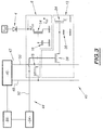
- the figure 1 represents control means 2 of the transmission of the transmitters 4 of the network according to a first embodiment of the invention. For the sake of simplification, only the means for controlling the addressing of a single transmitter have been illustrated in this figure.
- the control means 2 comprise a first addressing circuit 6 connected to a transmitter 4 of the network, addressing control means 8 of a transmitter column, selection control means 10 of a transmission line. transmitters, a control system 11 and a second addressing circuit 12 also connected to a transmitter 4.
- the first addressing circuit 6 comprises a current modulator 14, a storage capacitor 16 and a selection switch 18.
- the modulator 14 and the switch 18 are thin-film transistors in hydrogenated amorphous silicon. More precisely, they are n-type transistors. They comprise a drain, a gate and a source and are able to be traversed by a current flowing from their drain to their source, when a voltage greater than or equal to their trigger threshold voltage is applied between their gate and their source.
- transistors 14 and 18 are able to be traversed by a current flowing from their source to their drain.
- the drain of the modulator 14 is connected to the cathode of the transmitter 4.
- the anode of the transmitter 4 is connected to a DC voltage generator V dd suitable for supplying power.
- the source of the modulator 14 is connected to a ground electrode or to a negative voltage.
- the gate of the modulator 14 is connected to the source of the switch 18 and to one terminal of the storage capacitor 16.
- the other terminal of the capacitor 16 is connected to a ground electrode.
- the gate of the switch 18 is connected to the selection control means 10 and its drain is connected to the addressing control means 8.
- the addressing control means 8 of an emitter column comprise an emitter column addressing electrode 20 and an addressing control unit 22.
- the electrode 20 is connected on the one hand to the emitter column.
- control unit 22 and, on the other hand, the drain of the switch 18 of the first addressing circuits 6 of a column of transmitters.
- the selection control means 10 comprises a first selection electrode 24 and a second selection electrode 26 for each transmitter line as well as a selection control unit 28.
- first selection electrode 24 is connected to the control unit 28 and to the gate of the switch 18 of the first addressing circuits 6 of a line of transmitters.
- the second electrode 26 is connected to the control unit 28 and the gate of the switch 38 of the second addressing circuit 12 of a transmitter line.
- the control system 11 is connected to the addressing control unit 22 and to the selection control unit 28.
- the second addressing circuit 12 comprises the same components as the first addressing circuit 6, namely a current modulator 34, a storage capacitor 36 and a selection switch 38. These components are connected to each other in the same manner as in the first addressing circuit 6 and will not be described in detail.
- the current modulator 34 of the second addressing circuit 12 is connected to the cathode of the transmitter 4 at the node 32.
- the drain of the switch 38 is connected to the same addressing electrode 20 as the switch 18 and its gate is connected to the second selection electrode 26.
- the control system 11 is capable of transmitting digital image data and data relating to the bias voltage to the control unit 22 and a periodic selection signal to the control unit 28 at a predefined frequency.
- the addressing control unit 22 is capable of transmitting an address voltage V D representative of an image data item to all the emitters of a column via the electrode 20.
- the control unit of FIG. addressing 22 is also able to apply to the electrode 20 a voltage, called the bias voltage V p , of a polarization inverse to the polarization of the addressing voltage.
- This voltage is a predetermined negative voltage of a predetermined duration.
- the bias voltage V p is between -2 volts and -25 volts.
- the term "reverse or negative bias voltage” is used to denote a potential difference V gs between the gate and source electrodes of the modulator which is less than 0 Volt: V gs ⁇ 0V.
- the control unit 28 is able to apply a periodic selection voltage V S1 , V S2 to the gate of the switch 18 of the first addressing circuits 6 of a transmitter line or to the gate of the switch 38 of the second addressing circuit 12 of the same line of transmitters to allow the application of the addressing voltage V D or the bias voltage V p to the gate of the modulator 14 of the first addressing circuit 6 or to the gate of the modulator 34 second addressing circuit 12.
- FIGS. 2A to 2F illustrate the method of addressing a display screen according to the first embodiment of the invention.
- This method comprises a polarization programming step A of the modulator 34 of the second addressing circuit 12.
- the selection control unit 28 transmits to the second electrode 26, a selection voltage V s2 , as illustrated on FIG. Figure 2B .
- the selection switch 38 is unlocked by the application to its gate of this selection voltage V S2 .
- the addressing control unit 22 applies to the addressing electrode 20 a bias voltage V p of negative polarity (V gs ⁇ 0).
- V p bias voltage
- the bias voltage V p is applied to the gate of the current modulator 34 and to a terminal of the storage capacitor 36.
- the drain current I d2 which passed through the modulator 34 to supply the transmitter 4 during the previous frame, tends to now to 0 during this new frame as shown by the dashed curve of the figure 2E .
- the storage capacity 36 having previously stored a voltage V D applied during the previous frame is biased to the bias voltage V p , as shown in FIG. 2D figure ; as indicated by the dashed curve of this figure, the storage capacity 36 maintains this bias voltage at the gate of the modulator 34 during a polarization phase of the second addressing circuit 12 and until the end of the next step
- the steps B, C and D together constitute a polarization phase of the second addressing circuit 12.
- the trip threshold voltage of modulator 34 drifted by the application of an address voltage during the previous frame is again derived during the polarization phase and during the entire duration of the new frame, by applying the bias voltage V p but in a direction opposite to its previous drift.
- the bias voltage applied to the gate of the modulator 34 during the new frame makes it possible to reverse the drift of its trigger threshold voltage and to put it back to its initial value, that is to say to the value that it had before being derived by the application of an addressing voltage to its gate during the previous frame.
- the selection control unit 28 During the addressing programming step B of the modulator 14 of the first addressing circuit 6, the selection control unit 28 generates a selection voltage V S1 and applies it to the first electrode 24.
- the addressing control unit 22 transmits to the addressing electrode 20 an address voltage V Da representative of an image data item.
- the selection switch 18, at the intersection of the addressing electrode 20 and the first selection electrode 24, is unblocked and transmits the addressing voltage V Da to the modulator 14 and to the storage capacity 16 of the first circuit 6. Since the addressing voltage V Da is greater than the trigger threshold voltage of the modulator 14, a drain current I d1 is established between the drain and the source of the modulator 14 and therefore passes through the transmitter 4 as shown in the figure 2F .
- the capacitor 16 stores a potential representative of the addressing voltage V Da at the gate of the modulator 14 to maintain the luminance of the transmitter 4 during a time interval corresponding to the duration of an image frame. Thus, the transmitter 4 emits light during step C until the end of the image frame.
- the selection control unit 28 transmits a selection voltage V S1 to the first electrode 24.
- the addressing control unit 22 applies a bias voltage V p to the electrode 20.
- the selection switch 18, at the intersection of the first electrode 24 and the addressing electrode 20, is unlocked and this time transmits the bias voltage V p to the modulator 14 and the storage capacitor 16.
- the capacitance storage discharges and stores the charges transmitted by the bias voltage during a polarization phase E, F of the first addressing circuit 6, as shown in FIG. 2D figure .
- the drain current I d1 of the previous frame ceases to pass through the modulator 14.
- the trigger threshold voltage of the modulator 14 which has drifted and increased during the image frame will decrease during the new frame and especially at the course of step F.
- the next image frame starts with an addressing programming step E of the modulator 34 of the second addressing circuit 12.
- the selection control unit 28 applies to the electrode 26 a selection voltage V s2 .
- the addressing control unit 22 applies, parallel to the electrode 20, an addressing voltage V Db .
- the switch 38 of the second addressing circuit 12 is unlocked and the addressing voltage V Db , representative of an image data, is applied to the gate of the modulator 34 and to the terminal of the storage capacitor 36.
- a drain current I d2 is generated between the drain and the source of the modulator 34. This current has an amplitude proportional to the value of the image data to be transmitted during this image frame. This current flows through the light emitter 4 during step F until the end of the image frame.
- the transmitter 4 is supplied with current in turn by the first modulator 14 during an activation phase of the first addressing circuit, then by the second modulator 34 during a phase activating the second addressing circuit.
- the trigger threshold voltages of the modulator 14 of the first addressing circuit and the modulator 34 of the second addressing circuit are increased and then decreased in turn at each image frame. Such a device therefore advantageously makes it possible to compensate for the trigger threshold voltage drift of the modulators of the panel.
- An emitter 4 and the control means 40 of its transmission according to a second embodiment of the invention are represented on the figure 3 .
- control means 40 comprise first addressing circuits 6 and second addressing circuits 12, each connected to a transmitter 4 of the network, addressing control means 42 of a column d transmitters, selection control means 44 of a transmitter line and a control system 56.
- the first 6 and the second 12 addressing circuits comprise the same components, connected in the same way as the addressing circuits described in connection with the figure 1 . They are identified by the same references as on the figure 1 and will not be described below.
- the addressing control means 42 comprise an addressing control unit 46, a first addressing electrode 48 and a second addressing electrode 50 for each column of transmitters.
- the first addressing electrode 48 is connected to the control unit 46 and the drain of the switch 18 of all the first addressing circuits 6 of a column of transmitters.
- the second addressing electrode 50 is connected to the control unit 46 and to the drain of the switch 38 of the set of second addressing circuits 12 of a column of transmitters.
- the addressing unit 46 for addressing is able to send an address voltage V D1 on the first electrode 48 and concomitantly an address voltage V D2 on the second electrode 50.
- the selection control means 44 comprise a selection control unit 54 and, for each row of transmitters, a single selection electrode 52.
- the selection electrode 52 is connected to the control unit 54, to the gate of the switch 18 of the first addressing circuits 6 and to the gate of the switch 38 of the second addressing circuits 12 of a line of transmitters.
- the control system 56 is connected to the control unit 54 as well as to the control unit 46. This control system 56 is able to transmit to the control unit 46 digital image data and data. relating to the bias voltage. It is also able to transmit to the control unit 54 a periodic selection signal.
- This method comprises a step G of addressing addressing of the capacitor 16 and of the simultaneous polarization programming of the modulator 34.
- the control unit 46 transmits an address voltage V Da representative of an image data item to the first electrode 48 and a bias voltage V p to the second electrode 50.
- control unit 54 transmits a selection voltage V S to the selection electrode 52.
- the switch 18 of the first addressing circuit and the switch 38 of the second programming circuit are unlocked so that firstly, the bias voltage V p is applied to the gate of the modulator 34 and the terminal of the capacitor 36 and, secondly, the addressing voltage V Da is applied to the gate of the modulator 14 and to a terminal storage capacity 16.
- the storage capacitor 36 discharges and then charges at a negative potential equal to the bias voltage V p .
- This voltage maintained at the gate of the modulator 34 by the storage capacitor 36 aims to progressively reduce the trigger threshold voltage of the modulator 34 in particular during the step H.
- the drain current I d2 vanishes and remains zero during step H.
- the capacitor 16 charges at the potential V Da and a drain current I d1 is established between the drain and the source of the modulator 14.
- the transmitter 4 is supplied with the current I d1 during the step H until the end of the image frame.
- the transmitter 4 is therefore supplied with current by the first addressing circuit 6; the steps G and H together form an activation phase of the first addressing circuit. Furthermore, during the steps G and H, the bias voltage is applied to the gate of the modulator 34 to compensate for the drift of its trigger threshold voltage. The steps G and H therefore also form a polarization phase of the second addressing circuit.
- control unit 46 transmits a bias voltage V p to the first electrode 48 and an address voltage V Db representative of an image data at the second electrode 50.
- the switches 18 and 38 are simultaneously open by applying the selection voltage V S to the electrode 52.
- the bias voltage V p is transmitted to the gate of the modulator 14 and to the terminal of the capacitor 16.
- the capacitor 16 is discharge and then charge negatively.
- the drain current I d1 vanishes and remains zero during step J.
- the bias voltage V p is applied to the gate of the modulator 14.
- the steps I and J together form a polarization phase of the first addressing circuit 6.
- the addressing voltage V Db is applied to the gate of the modulator 34 and to a terminal of the capacitor 36.
- This voltage maintained at the gate of the modulator 34 by the capacitor 36, generates a drain current I d2 which feeds transmitter 4 during step J and up to the next step of programming new image data.
- the transmitter 4 is supplied with current by the second addressing circuit 12; these steps together form an activation phase of the second addressing circuit.
- the emitter 4 is thus supplied in turn by the modulated current, by the modulator 14, then by the modulator 34.
- the first 6 and second 12 addressing circuits are alternately activated to power the transmitter 4.
- the modulator 34 When the modulator 14 supplies the transmitter 4, the modulator 34 is polarized by applying a bias voltage corresponding to a high negative voltage to its gate so that the tripping threshold voltage of the modulator 34 derived during the previous phase returns to its initial value.
- the modulator 14 when the modulator 34 supplies the transmitter 4, the modulator 14 is biased by this same negative bias voltage so that its trigger threshold voltage having previously drifted in one direction, drifts in an opposite direction.
- the addressing method associated with each transmitter contributes to compensating for variations in the tripping threshold of the modulators of a display screen.
- the polarization and activation phases are carried out simultaneously and have equal durations.
- the control means are also able to control the modulators 14 and 34 so that the polarization and activation phases of the first and second circuits, although performed simultaneously, have different durations.
- the bias voltage applied to one or the other of the modulators of a transmitter varies from one image frame to another, as a function of the addressing voltage applied to the this modulator during the previous frame; preferably, this bias voltage is equal but of opposite sign to said addressing voltage of the previous frame.
Landscapes
- Engineering & Computer Science (AREA)
- Physics & Mathematics (AREA)
- Computer Hardware Design (AREA)
- General Physics & Mathematics (AREA)
- Theoretical Computer Science (AREA)
- Control Of Indicators Other Than Cathode Ray Tubes (AREA)
- Electroluminescent Light Sources (AREA)
Applications Claiming Priority (2)
| Application Number | Priority Date | Filing Date | Title |
|---|---|---|---|
| FR0315629 | 2003-12-31 | ||
| PCT/FR2004/003104 WO2005073948A1 (fr) | 2003-12-31 | 2004-12-02 | Ecran d'affichage d'images et procede d'adressage de cet ecran. |
Publications (2)
| Publication Number | Publication Date |
|---|---|
| EP1700290A1 EP1700290A1 (fr) | 2006-09-13 |
| EP1700290B1 true EP1700290B1 (fr) | 2019-01-16 |
Family
ID=34814552
Family Applications (1)
| Application Number | Title | Priority Date | Filing Date |
|---|---|---|---|
| EP04805623.8A Expired - Fee Related EP1700290B1 (fr) | 2003-12-31 | 2004-12-02 | Ecran d'affichage d'images et procede d'adressage de cet ecran |
Country Status (5)
| Country | Link |
|---|---|
| EP (1) | EP1700290B1 (zh) |
| JP (1) | JP5074769B2 (zh) |
| KR (1) | KR101205912B1 (zh) |
| CN (1) | CN100456346C (zh) |
| WO (1) | WO2005073948A1 (zh) |
Families Citing this family (11)
| Publication number | Priority date | Publication date | Assignee | Title |
|---|---|---|---|---|
| KR101066414B1 (ko) * | 2004-05-19 | 2011-09-21 | 재단법인서울대학교산학협력재단 | 유기발광소자의 구동소자 및 구동방법과, 이를 갖는표시패널 및 표시장치 |
| JP5121118B2 (ja) * | 2004-12-08 | 2013-01-16 | 株式会社ジャパンディスプレイイースト | 表示装置 |
| KR101142996B1 (ko) | 2004-12-31 | 2012-05-08 | 재단법인서울대학교산학협력재단 | 표시 장치 및 그 구동 방법 |
| FR2895130A1 (fr) | 2005-12-20 | 2007-06-22 | Thomson Licensing Sas | Procede de pilotage d'un panneau d'affichage par couplage capacitif |
| FR2895131A1 (fr) | 2005-12-20 | 2007-06-22 | Thomson Licensing Sas | Panneau d'affichage et procede de pilotage avec couplage capacitif transitoire |
| FR2900492B1 (fr) | 2006-04-28 | 2008-10-31 | Thales Sa | Ecran electroluminescent organique |
| EP1863001A1 (en) | 2006-06-01 | 2007-12-05 | Thomson Licensing | Video display device and operating method therefore |
| EP1863005B1 (en) * | 2006-06-01 | 2010-08-04 | Thomson Licensing | Video display device and operating method therefore |
| US9116593B2 (en) | 2007-07-06 | 2015-08-25 | Qualcomm Incorporated | Single-axis window manager |
| JP5178492B2 (ja) * | 2007-12-27 | 2013-04-10 | 株式会社半導体エネルギー研究所 | 表示装置および当該表示装置を具備する電子機器 |
| KR100939211B1 (ko) * | 2008-02-22 | 2010-01-28 | 엘지디스플레이 주식회사 | 유기발광다이오드 표시장치와 그 구동방법 |
Citations (2)
| Publication number | Priority date | Publication date | Assignee | Title |
|---|---|---|---|---|
| JP2001034231A (ja) * | 1999-07-22 | 2001-02-09 | Seiko Epson Corp | El表示装置 |
| EP1111574A2 (en) * | 1999-12-24 | 2001-06-27 | Sel Semiconductor Energy Laboratory Co., Ltd. | Electroluminescent display device |
Family Cites Families (10)
| Publication number | Priority date | Publication date | Assignee | Title |
|---|---|---|---|---|
| JP2689916B2 (ja) * | 1994-08-09 | 1997-12-10 | 日本電気株式会社 | アクティブマトリクス型電流制御型発光素子の駆動回路 |
| US5714968A (en) * | 1994-08-09 | 1998-02-03 | Nec Corporation | Current-dependent light-emitting element drive circuit for use in active matrix display device |
| JP3308880B2 (ja) * | 1997-11-07 | 2002-07-29 | キヤノン株式会社 | 液晶表示装置と投写型液晶表示装置 |
| US20020030647A1 (en) * | 2000-06-06 | 2002-03-14 | Michael Hack | Uniform active matrix oled displays |
| JP3877049B2 (ja) * | 2000-06-27 | 2007-02-07 | 株式会社日立製作所 | 画像表示装置及びその駆動方法 |
| KR100370095B1 (ko) * | 2001-01-05 | 2003-02-05 | 엘지전자 주식회사 | 표시 소자의 액티브 매트릭스 방식의 구동 회로 |
| TW518528B (en) * | 2001-01-08 | 2003-01-21 | Chi Mei Optoelectronics Corp | Driving method of active matrix electro-luminescent display |
| US6858989B2 (en) * | 2001-09-20 | 2005-02-22 | Emagin Corporation | Method and system for stabilizing thin film transistors in AMOLED displays |
| KR100489272B1 (ko) * | 2002-07-08 | 2005-05-17 | 엘지.필립스 엘시디 주식회사 | 유기 전계발광소자 및 그의 구동방법 |
| TWI254898B (en) * | 2003-10-02 | 2006-05-11 | Pioneer Corp | Display apparatus with active matrix display panel and method for driving same |
-
2004
- 2004-12-02 KR KR1020067012112A patent/KR101205912B1/ko active IP Right Grant
- 2004-12-02 CN CNB2004800391974A patent/CN100456346C/zh not_active Expired - Fee Related
- 2004-12-02 EP EP04805623.8A patent/EP1700290B1/fr not_active Expired - Fee Related
- 2004-12-02 WO PCT/FR2004/003104 patent/WO2005073948A1/fr not_active Application Discontinuation
- 2004-12-02 JP JP2006546220A patent/JP5074769B2/ja not_active Expired - Fee Related
Patent Citations (2)
| Publication number | Priority date | Publication date | Assignee | Title |
|---|---|---|---|---|
| JP2001034231A (ja) * | 1999-07-22 | 2001-02-09 | Seiko Epson Corp | El表示装置 |
| EP1111574A2 (en) * | 1999-12-24 | 2001-06-27 | Sel Semiconductor Energy Laboratory Co., Ltd. | Electroluminescent display device |
Non-Patent Citations (2)
| Title |
|---|
| HACK M ET AL: "Drain-Bias Dependence of Threshold Voltage Stability of Amorphous Silicon TFTs", IEEE ELECTRON DEVICE LETTERS, IEEE SERVICE CENTER, NEW YORK, NY, US, vol. 25, no. 4, 1 April 2004 (2004-04-01), pages 188 - 190, XP011109652, ISSN: 0741-3106, DOI: 10.1109/LED.2004.825154 * |
| KIM J H ET AL: "THRESHOLD VOLTAGE SHIFT OF AMORPHOUS SILICON THIN FILM TRANSISTORS WITH ATMOSPHERIC PRESSURE CHEMICAL VAPOR DEPOSITION SILICON DIOXIDE", APPLIED PHYSICS LETTERS, A I P PUBLISHING LLC, US, vol. 64, no. 18, 2 May 1994 (1994-05-02), pages 2362/2363, XP000440965, ISSN: 0003-6951, DOI: 10.1063/1.111615 * |
Also Published As
| Publication number | Publication date |
|---|---|
| KR20060135670A (ko) | 2006-12-29 |
| JP5074769B2 (ja) | 2012-11-14 |
| EP1700290A1 (fr) | 2006-09-13 |
| JP2007519949A (ja) | 2007-07-19 |
| CN100456346C (zh) | 2009-01-28 |
| KR101205912B1 (ko) | 2012-11-28 |
| WO2005073948A1 (fr) | 2005-08-11 |
| CN1902675A (zh) | 2007-01-24 |
Similar Documents
| Publication | Publication Date | Title |
|---|---|---|
| EP2013863B1 (fr) | Ecran electroluminescent organique | |
| EP1851747B1 (fr) | Circuit d'adressage de pixels et procede de controle d'un tel circuit | |
| FR2857146A1 (fr) | Dispositif d'affichage d'images a matrice active | |
| EP1700290B1 (fr) | Ecran d'affichage d'images et procede d'adressage de cet ecran | |
| FR2884639A1 (fr) | Panneau d'affichage d'images a matrice active, dont les emetteurs sont alimentes par des generateurs de courant pilotables en tension | |
| WO2005086130A1 (fr) | Dispositif ameliore d'adressage de pixels | |
| EP2277164B1 (fr) | Dispositif d'affichage amélioré à base de pixels à coordonnées chromatiques variables | |
| WO2007071679A1 (fr) | Procede de pilotage d'un panneau d'affichage avec depolarisation | |
| EP1964095B1 (fr) | Panneau d'affichage et procede de pilotage avec couplage capacitif transitoire | |
| EP1964094B1 (fr) | Procede de pilotage d'un panneau d'affichage par couplage capacitif | |
| EP1771838B1 (fr) | Dispositif d'affichage d'images et procede de commande d'un dispositif d'affichage | |
| EP1864275B1 (fr) | Dispositif d'affichage d'images et procede de pilotage de celui-ci. | |
| EP1697920B1 (fr) | Dispositif d'affichage d'images a matrice active oled | |
| EP1697919B1 (fr) | Ecran d'affichage d'images | |
| EP1697997B1 (fr) | Ecran d'affichage d'images et procede de pilotage de cet ecran | |
| FR2843225A1 (fr) | Dispositif de visualisation d'images a matrice active et a compensation de seuil de declenchement | |
| MXPA06007404A (en) | Image display screen and method of addressing said screen |
Legal Events
| Date | Code | Title | Description |
|---|---|---|---|
| PUAI | Public reference made under article 153(3) epc to a published international application that has entered the european phase |
Free format text: ORIGINAL CODE: 0009012 |
|
| 17P | Request for examination filed |
Effective date: 20060419 |
|
| AK | Designated contracting states |
Kind code of ref document: A1 Designated state(s): DE FR GB |
|
| DAX | Request for extension of the european patent (deleted) | ||
| RBV | Designated contracting states (corrected) |
Designated state(s): DE FR GB |
|
| RAP1 | Party data changed (applicant data changed or rights of an application transferred) |
Owner name: THOMSON LICENSING |
|
| 17Q | First examination report despatched |
Effective date: 20100730 |
|
| GRAP | Despatch of communication of intention to grant a patent |
Free format text: ORIGINAL CODE: EPIDOSNIGR1 |
|
| INTG | Intention to grant announced |
Effective date: 20180808 |
|
| GRAS | Grant fee paid |
Free format text: ORIGINAL CODE: EPIDOSNIGR3 |
|
| GRAA | (expected) grant |
Free format text: ORIGINAL CODE: 0009210 |
|
| AK | Designated contracting states |
Kind code of ref document: B1 Designated state(s): DE FR GB |
|
| REG | Reference to a national code |
Ref country code: GB Ref legal event code: FG4D Free format text: NOT ENGLISH |
|
| REG | Reference to a national code |
Ref country code: DE Ref legal event code: R096 Ref document number: 602004053648 Country of ref document: DE |
|
| REG | Reference to a national code |
Ref country code: DE Ref legal event code: R097 Ref document number: 602004053648 Country of ref document: DE |
|
| PLBE | No opposition filed within time limit |
Free format text: ORIGINAL CODE: 0009261 |
|
| STAA | Information on the status of an ep patent application or granted ep patent |
Free format text: STATUS: NO OPPOSITION FILED WITHIN TIME LIMIT |
|
| 26N | No opposition filed |
Effective date: 20191017 |
|
| REG | Reference to a national code |
Ref country code: DE Ref legal event code: R119 Ref document number: 602004053648 Country of ref document: DE |
|
| GBPC | Gb: european patent ceased through non-payment of renewal fee |
Effective date: 20191202 |
|
| PG25 | Lapsed in a contracting state [announced via postgrant information from national office to epo] |
Ref country code: DE Free format text: LAPSE BECAUSE OF NON-PAYMENT OF DUE FEES Effective date: 20200701 Ref country code: FR Free format text: LAPSE BECAUSE OF NON-PAYMENT OF DUE FEES Effective date: 20191231 Ref country code: GB Free format text: LAPSE BECAUSE OF NON-PAYMENT OF DUE FEES Effective date: 20191202 |