EP1684434A1 - Thermometer coding circuitry - Google Patents
Thermometer coding circuitry Download PDFInfo
- Publication number
- EP1684434A1 EP1684434A1 EP06008707A EP06008707A EP1684434A1 EP 1684434 A1 EP1684434 A1 EP 1684434A1 EP 06008707 A EP06008707 A EP 06008707A EP 06008707 A EP06008707 A EP 06008707A EP 1684434 A1 EP1684434 A1 EP 1684434A1
- Authority
- EP
- European Patent Office
- Prior art keywords
- dimension
- row
- signal
- cells
- col
- Prior art date
- Legal status (The legal status is an assumption and is not a legal conclusion. Google has not performed a legal analysis and makes no representation as to the accuracy of the status listed.)
- Withdrawn
Links
- 230000008859 change Effects 0.000 description 22
- 238000000034 method Methods 0.000 description 10
- 230000000295 complement effect Effects 0.000 description 9
- 101100115778 Caenorhabditis elegans dac-1 gene Proteins 0.000 description 6
- 238000003491 array Methods 0.000 description 4
- 230000008901 benefit Effects 0.000 description 4
- 230000008878 coupling Effects 0.000 description 4
- 238000010168 coupling process Methods 0.000 description 4
- 238000005859 coupling reaction Methods 0.000 description 4
- 230000009849 deactivation Effects 0.000 description 4
- 230000004044 response Effects 0.000 description 4
- 230000004913 activation Effects 0.000 description 3
- 230000001934 delay Effects 0.000 description 3
- 230000008569 process Effects 0.000 description 3
- 239000000758 substrate Substances 0.000 description 3
- 238000010276 construction Methods 0.000 description 2
- 230000007423 decrease Effects 0.000 description 2
- 229920005994 diacetyl cellulose Polymers 0.000 description 2
- 238000009795 derivation Methods 0.000 description 1
- 230000000694 effects Effects 0.000 description 1
- 230000036039 immunity Effects 0.000 description 1
- 239000011159 matrix material Substances 0.000 description 1
- 230000002093 peripheral effect Effects 0.000 description 1
Images


Classifications
-
- H—ELECTRICITY
- H03—ELECTRONIC CIRCUITRY
- H03M—CODING; DECODING; CODE CONVERSION IN GENERAL
- H03M1/00—Analogue/digital conversion; Digital/analogue conversion
- H03M1/66—Digital/analogue converters
- H03M1/68—Digital/analogue converters with conversions of different sensitivity, i.e. one conversion relating to the more significant digital bits and another conversion to the less significant bits
- H03M1/682—Digital/analogue converters with conversions of different sensitivity, i.e. one conversion relating to the more significant digital bits and another conversion to the less significant bits both converters being of the unary decoded type
- H03M1/685—Digital/analogue converters with conversions of different sensitivity, i.e. one conversion relating to the more significant digital bits and another conversion to the less significant bits both converters being of the unary decoded type the quantisation value generators of both converters being arranged in a common two-dimensional array
-
- H—ELECTRICITY
- H03—ELECTRONIC CIRCUITRY
- H03M—CODING; DECODING; CODE CONVERSION IN GENERAL
- H03M7/00—Conversion of a code where information is represented by a given sequence or number of digits to a code where the same, similar or subset of information is represented by a different sequence or number of digits
- H03M7/14—Conversion to or from non-weighted codes
- H03M7/16—Conversion to or from unit-distance codes, e.g. Gray code, reflected binary code
- H03M7/165—Conversion to or from thermometric code
-
- H—ELECTRICITY
- H03—ELECTRONIC CIRCUITRY
- H03M—CODING; DECODING; CODE CONVERSION IN GENERAL
- H03M1/00—Analogue/digital conversion; Digital/analogue conversion
- H03M1/66—Digital/analogue converters
- H03M1/74—Simultaneous conversion
- H03M1/742—Simultaneous conversion using current sources as quantisation value generators
- H03M1/747—Simultaneous conversion using current sources as quantisation value generators with equal currents which are switched by unary decoded digital signals
Definitions
- thermometer coding circuitry for use, for example, in digital-to-analog converters.
- FIG. 1 of the accompanying drawings shows parts of a conventional digital-to-analog converter (DAC) of the so-called "current-steering" type.
- the DAC 1 is designed to convert an m-bit digital input word (D1-Dm) into a corresponding analog output signal.
- the DAC 1 further includes a plurality of differential switching circuits 4 1 to 4 n corresponding respectively to the n current sources 2 1 to 2 n . Each differential switching circuit 4 is connected to its corresponding current source 2 and switches the current I produced by the current source either to a first terminal, connected to a first connection line A of the converter, or a second terminal connected to a second connection line B of the converter.
- Each differential switching circuit 4 receives one of a plurality of control signals T1 to Tn (called “thermometer-coded signals” for reasons explained hereinafter) and selects either its first terminal or its second terminal in accordance with the value of the signal concerned.
- a first output current I A of the DAC 1 is the sum of the respective currents delivered to the differential-switching-circuit first terminals
- a second output current I B of the DAC 1 is the sum of the respective currents delivered to the differential-switching-circuit second terminals.
- the analog output signal is the voltage difference V A -V B between a voltage V A produced by sinking the first output current I A of the DAC 1 into a resistance R and a voltage V B produced by sinking the second output current I B of the converter into another resistance R.
- thermometer-coded signals T1 to Tn are derived from the binary input word D1-Dm by a binary-thermometer decoder 6.
- the decoder 6 operates as follows.
- thermometer-coded signals T1-Tn are such that each of the differential switching circuits 4 1 to 4 n selects its second terminal so that all of the current sources 2 1 to 2 n are connected to the second connection line B.
- the analog output signal V A -V B -nIR.
- thermometer-coded signals T1 to Tn produced by the decoder 6 are such that more of the differential switching circuits select their respective first terminals (starting from the differential switching circuit 4 1 ) without any differential switching circuit that has already selected its first terminal switching back to its second terminal.
- the first i differential switching circuits 4 1 to 4 i select their respective first terminals, whereas the remaining n-i differential switching circuits 4 i+1 to 4 n select their respective second terminals.
- the analog output signal V A -V B is equal to (2i-n) IR.
- thermometer-coded signals T1 to Tn generated by the binary-thermometer decoder 6 follow a so-called thermometer code in which it is known that when an rth-order signal Tr is activated (set to "1"), all of the lower-order signals T1 to Tr-1 will also be activated.
- Thermometer coding is popular in DACs of the current-steering type because, as the binary input word increases, more current sources are switched to the first connection line A without any current source that is already switched to that line A being switched to the other line B. Accordingly, the input/output characteristic of the DAC is monotonic and the glitch impulse resulting from a change of 1 in the input word is small.
- each cell CL ij is arranged in an 8 x 8 square array having eight rows and eight columns.
- the first digit of the suffix applied to each cell denotes the row in which the cell is located and the second digit of the suffix denotes the column in which the cell is located.
- the cell CL 18 is the cell in row 1, column 8.
- Each cell CL ij includes its own current source 2 and its own differential switching circuit 4.
- the respective first terminals of the cells of the array are connected together to a first connection line A of the DAC and the respective second terminals of the cells of the array are connected together to a second connection line B of the DAC, as in the Figure 1 DAC.
- thermometer-coded signals In order to avoid having to generate and supply different respective thermometer-coded signals to all the cells of the array, a two-stage decoding process is adopted to convert the binary input word D1-D6 into the respective thermometer-coded control signals T required by the differential switching circuits 4 in the different cells.
- the first stage of this two-stage decoding process is carried out by respective row and column decoders 12 and 14, and the second stage is carried out by a local decoder 16 provided for each cell.
- the three lower-order bits D1-D3 of the binary input word are applied to the column decoder 14 which derives therefrom seven thermometer-coded column selection signals in accordance with Figure 2.
- the row decoder 12 receives the three higher-order bits D4-D6 of the input word and derives therefrom seven thermometer-coded row selection signals, also in accordance with Figure 2.
- the row and column selection signals are distributed to the cells of the array.
- the output signals are not all deactivated when the input-signal value is changed from the second value to the next-highest value. Accordingly, a large glitch is avoided at the second value.
- At most one of the first-set output signals is activated or deactivated. This keeps glitches to a minimum.
- the first-set output signals it is not necessary for there to be a change in the first-set output signals for every unit change in the input-signal value. For example, in one preferred embodiment, when the input signal decreases in value from the said second value to the next-lowest value, none of the first-set output signals is changed. Such an embodiment can be used, for example, when there is another set of output signals derived from the input signal, which other set undergoes an output-signal change when the input-signal value changes from the second value to the next-lowest value.
- the predetermined activation and deactivation sequences for the first-set output signals are such that the first output signal to be activated in the activation sequence is the last output signal to be deactivated in the deactivation sequence.
- the activation and deactivation sequences could be the same.
- the coding circuitry is further operable to produce a second set of thermometer-coded output signals in dependence upon the said binary input signal such that, as the input signal increases progressively in value from the said first value to the said second value, the second-set output signals are deactivated in a predetermined sequence and, as the input signal increases progressively in value from the said second value to the said third value, the second-set output signals are activated in a predetermined sequence.
- each output signal of the first set can be regarded as having an individually-corresponding output signal of the second set, which two output signals can be delivered as a output-signal pair to a line of circuit elements, e.g. a column in a two-dimensional array of the elements.
- Even-numbered circuit elements along the column use as their selection signal one output signal of the pair (e.g. the first-set output signal) whereas odd-numbered circuit elements of the column use as their selection signal the other output signal of the pair (e.g. the second-set output signal).
- the input-signal value changes from any value to the next-highest value or the next-lowest value at most only one second-set output signal is activated or deactivated.
- the input signal decreases from the said second value to the next-lowest value it is possible that none of the second-set output signals is changed, for example when there is another set of output signals derived from the input signal that undergoes an output-signal change when the input-signal value changes from the second value to the next-lowest value.
- the number of output signals that are deactivated in one of the first and second output-signal sets is equal to the number of output signals that are activated in the other of the first and second output-signal sets. This means that the changes in the two sets of output signals cancel one another out for noise purposes.
- cell array circuitry including: a plurality of cells arrayed logically (i.e. not necessarily physically) in rows and columns, each cell of the array having local decoder means connected for receiving a row selection signal corresponding to its row and a column selection signal corresponding to its column, and operable, in dependence upon the received row and column selection signals, to produce a control signal for use in controlling a predetermined operation of the cell; a row decoder for producing the said row selection signals corresponding respectively to the said rows; and a column decoder, comprising coding circuitry embodying the aforesaid first aspect of the present invention, the said column selection signals corresponding respectively to the said columns being provided by the said output signals of the coding circuitry.
- the cells may contain any suitable circuitry, for example current sources or current sinks, resistance elements, capacitance elements, mixers etc.
- the predetermined operation may be any type of operation of the cell.
- it could be a switching or selection operation for switching on or off, or controlling the output path of, an (analog) output signal of the cell.
- the local decoder means associated with each cell can have a simple construction (e.g. two logic gates), contributing to low signal propagation delays as well as low cost. It is not necessary for the local decoder means to be located in its associated cell.
- each cell may also be connected for receiving the row selection signal corresponding to the next row of the array so as to enable the local decoder means to respond to the column selection signal for the cell differently depending on whether or not the row in which the cell is located is the highest-numbered row to be selected.
- each cell only receives one such column selection signal.
- the array of cells may be regarded as having alternate first and second rows (logically alternate, not necessarily physically alternate).
- the local decoder means in first-row cells is different from the local decoder means in second-row cells.
- the local decoder means in each first-row cell is operable to produce its said control signal when the said row selection signal corresponding to the cell's row and the said column selection signal corresponding to the cell's column are both activated or when the said row selection signal corresponding to the next row is activated.
- the local decoder means in each second-row cell is operable to produce its said control signal when the said row selection signal corresponding to the cell's row is activated and the said column selection signal corresponding to the cell's column is deactivated or when the said row selection signal corresponding to the next row is activated.
- each column can have respective first and second column selection signals corresponding to the column concerned, the first column selection signals corresponding to the different columns being provided respectively by the first-set output signals of the coding circuitry and the second column selection signals corresponding to the different columns being provided respectively by the second-set output signals of the coding circuitry.
- the cell array can then be regarded as having alternate first and second rows (logically alternate, not necessarily physically alternate).
- the local decoder means of first-row cells of the column concerned are connected to receive the said first column selection signal corresponding to the column concerned, and the local decoder means of second-row cells of the column concerned are connected to receive the second column selection signal corresponding to the column concerned.
- the selection sequences in the first and second rows are the same, even though each local decoder means only receives one column selection signal. If the cells are arrayed physically (as well as logically) in rows and columns, the distribution of selection signals is still convenient as only two column selection signals per column are required.
- the row decoder is connected for receiving a first portion (e.g. two or more most-significant bits) of a binary input-word signal applied to the cell array circuitry and produces the said row selection signals in dependence upon the first portion, and the said column decoder is connected for receiving a second portion (e.g. two or more least-significant bits) of that binary input-word signal, which portion constitutes the said binary input signal of the said coding circuitry.
- a first portion e.g. two or more most-significant bits
- the said column decoder is connected for receiving a second portion (e.g. two or more least-significant bits) of that binary input-word signal, which portion constitutes the said binary input signal of the said coding circuitry.
- a digital-to-analog converter including cell array circuitry embodying the aforesaid second aspect of the invention, wherein each of the said cells comprises a current source or current sink and a switch circuit having an input connected to the current source/sink of the cell and also having respective first and second outputs, and operable selectively, in dependence upon the said control signal, to connect its said input to its said first output or to its said second output.
- the three sets of output signals can enable a small total number of output signals to be used to select circuit elements of a large array (logical array, not necessarily physical) using desirably simple logic.
- the propagation delays associated with the coding circuitry can be desirably uniform and short.
- the first, second and third binary input signals may be provided from different respective sources. Preferably, however, at least two, and more preferably all three, of the said first, second and third binary input signals are derived from a common input-word signal. It is convenient to be able to select circuit elements from a single input signal.
- the first, second and third binary input signals may be derived from different respective portions (e.g. most-significant, middle-order, and least-significant bits) of the said common input-word signal.
- the output-signal sets may embody conventional thermometer codes.
- the output-signal set derived by at least one of the said first, second and third coding means is preferably a smoothed output-signal set of the type produced by coding circuitry embodying the aforesaid first aspect of the invention. This reduces glitches associated with the selection signals of a set all changing at certain input-signal values.
- each coding means that derives such a smoothed output-signal set is also preferably operable to derive two such smoothed sets of the thermometer-coded output signals. This has advantages in ensuring consistency in the selection sequences of different lines of the circuit elements.
- cell array circuitry including: a plurality of cells arrayed logically (not necessarily physically as well) in respective first, second and third dimensions (e.g. row, column and depth directions), each cell of the array having local decoder means connected for receiving a first-dimension selection signal (e.g. a row selection signal) corresponding to its first-dimension position in the array and a second-dimension selection signal (e.g. a column selection signal) corresponding to its second-dimension position in the array and a third-dimension selection signal (e.g.
- a depth selection signal corresponding to its third-dimension position in the array, and operable, in dependence upon the received selection signals, to produce a control signal for use in controlling a predetermined operation of the cell; and coding circuitry embodying the aforesaid fourth aspect of the present invention, the said first-dimension, second-dimension and third-dimension selection signals being provided by the said first, second and third output-signal sets respectively.
- Each cell is preferably also connected for receiving the row selection signal corresponding to the next row of the array and the column selection signal corresponding to the next column of the array.
- This can enable the local decoder means to respond to the column selection signal for its cell differently depending on whether or not the row in which the cell is located is the highest-numbered row to be selected, and to respond to the depth selection signal for its cell differently depending on whether or not the column in which the cell is located is the highest-numbered column to be selected.
- the third coding means in the coding circuitry are operable to produce two such smoothed output-signal sets serving to provide, for each third-dimension position, a first third-dimension selection signal corresponding to that position and a second third-dimension selection signal corresponding to that position.
- the cell array can be considered as having alternate (logically alternate, not necessarily physically alternate) first and second second-dimension positions.
- the local decoder means of cells at the first second-dimension positions are connected to receive the said first third-dimension selection signal corresponding to the third-dimension position concerned, and the local decoder means of cells at the second second-dimension positions are connected to receive the said second third-dimension selection signal corresponding to the third-dimension position concerned. This enables the selection sequences in the second-dimension lines (e.g. the columns) to be the same.
- the said second coding means in the coding circuitry are operable to produce two such smoothed output-signal sets serving to provide, for each second-dimension position, a first second-dimension selection signal corresponding to that position and a second second-dimension selection signal corresponding to that position.
- the cell array can be regarded as having alternate first and second first-dimension positions.
- the local decoder means of cells at the first first-dimension positions are connected to receive the said first second-dimension selection signal corresponding to the second-dimension position concerned, and the local decoder means cells at the second first-dimension positions are connected to receive the said second second-dimension selection signal corresponding to the second-dimension position concerned. This enables the selection sequences in the first-dimension lines (e.g. the rows) to be the same.
- Embodiments of the aforesaid third or sixth aspect of the present invention can provide a current-steered DAC in which glitches in the analog output signal are reduced highly effectively.
- the current source/sink circuits of the cells may be located together in a physical array, with the local decoder means and switch circuits located separately from the physical array, e.g. as peripheral circuits, so as to isolate the analog and digital circuitry and thereby improve noise immunity. Also, by concentrating the current source/sink circuits together in one place it is possible to improve the matching between the closely-proximate source/sink circuits.
- the DAC may be of the fully or partially segmented type, in which case the respective current sources/sinks of the said cells source/sink identical currents. Alternatively, the currents sourced/sunk by different cells may be different from one another.
- One of the first and second outputs of each switch circuit may be connected to a fixed-potential line such as ground, the other switch-element outputs being connected in common to a summing path of the converter.
- the respective first outputs of the cells are connected together to a first summing path of the converter and the respective second outputs of the cells are connected together to a second summing path of the converter.
- the analog output signal of the converter is of the differential type which has advantages in terms of connecting the DAC to further circuitry for processing the analog output.
- the differential output signal can be delivered by long signal lines to a transformer or the like without significant noise-related problems.
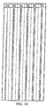
- FIG 4 shows an arrangement of cells in eight rows and eight columns, suitable for use in a DAC according to a first embodiment of the present invention.
- each cell includes a current source 2 and a differential switching circuit 4 which, in accordance with a control signal T applied to it, selects either to deliver the current I generated by the current source 2 to a first output terminal OUT A of the cell or to a second output terminal OUT B of the cell.
- the respective output terminals OUT A of the different cells are connected together to a first summing path (not shown) and the respective output terminals OUT B of the different cells are also connected together to a second summing path (not shown).
- the numbers allocated to the cells in Figure 4 denote the order in which the cells are caused to change from selecting their respective second output terminals to selecting their respective first output terminals as the binary input word of the DAC increases in value.
- the input word has the value 13
- the first 14 cells (0 to 13) select their first output terminals and the remaining cells (14 to 63) select their second output terminals.
- Cell 0 always selects its first output terminal in this embodiment.
- Each cell further comprises a local decoder 26 which, in this embodiment, comprises a two-input AND gate 28 and a two-input OR gate 30.
- the local decoder 26 of the cell receives first and second row signals r n+1 and r n and a column signal c n .
- the two row signals r n+1 and r n and the column signal c n applied to the local decoder 26 of each cell are provided by a set of "normal" thermometer-coded row selection signals ROW 0-6 and by two sets of “smoothed" thermometer-coded column selection signals COL A0 ⁇ 6 and COL B0 ⁇ 6 , as shown schematically in Figure 4.
- thermometer-coded row selection signals ROW 0 to ROW 6 correspond respectively to rows 0 to 6 of the Figure 4 cell array.
- the cells of the row receive, as the first row signal r n+1 , the row selection signal corresponding to the row concerned.
- the first row signal r n+1 for the cells of row 7 is simply set permanently to logic level "0".
- the cells of the row also receive, as the second row signal r n , the row selection signal corresponding to the preceding row of the cell array.
- the second row signal r n for all of the cells of the row is simply set permanently to logic level "1".
- the eight cells numbered 16 to 23 of row 2 each receive as the first row signal r n+1 the row selection signal ROW 2 corresponding to that row and receive as the second row signal r n the row selection signal ROW 1 corresponding to the preceding row 1 of the cell array.
- thermometer-coded column selection signals COL A and COL B there are two sets of thermometer-coded column selection signals COL A and COL B.
- Each of columns 1 to 7 has a corresponding COL A selection signal and a corresponding COL B selection signal.
- column 1 has a first corresponding column selection signal COL A0 and a second corresponding column selection signal COL B0.
- the cells of column 1 each have the column signal c n set permanently to logic "1".
- the DAC according to the first embodiment comprises an input latch 32 to which a six-bit binary input word D0-D5 is applied.
- the input latch 32 latches each bit D0 to D5 of the binary input word in dependence upon a clock signal CLK applied to the latch 32.
- the latch has six pairs of mutually-complementary outputs S0, S ⁇ 0 S1, S ⁇ 1,... S5, S ⁇ 5 corresponding respectively to the different bits D0 to D5 of the binary input word.
- the three lower-order outputs S0/S ⁇ 0, S1/S ⁇ 1 and S2/S ⁇ 2 are connected to respective complementary inputs I0/I ⁇ 0, I1/I ⁇ 1 and I2/I ⁇ 2 of a column decoder 34.
- a further input I3 of the column decoder 34 is connected to the output S3 of the input latch 32.
- the three higher-order outputs S3/S ⁇ 3, S4/S ⁇ 4 and S5/S ⁇ 5 are applied to respective complementary inputs I0/I ⁇ 0, I1/I ⁇ 1 and I2/I ⁇ 2 of a row decoder 36.
- each pair of complementary inputs of the column decoder 34 is connected to a different multiplexer M0 to M2.
- a selection input of each multiplexer M0 to M2 is connected to the I3 input of the column decoder 34.
- the multiplexer M0 produces an output signal C
- the multiplexer M1 produces an output signal B
- the multiplexer M2 produces an output signal A.
- each multiplexer M0 to M2 selects one of its two complementary inputs according to the value of the signal applied to the I3 input of the column decoder 34. For example, the multiplexer M0 selects the I0 input when the I3 input is 0 and selects the I ⁇ 0 input when the I3 input is 1. The signal at the selected input is delivered by the multiplexer M0 as the output signal C thereof.
- the multiplexers M1 and M2 function in a similar manner to the multiplexer M0.
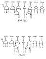
- the first set of column selection signals COL A0 to COL A6 is generated by a first group of gates GA1 as shown in Figure 7(B).
- the column selection signal COL A0 is generated by a three-input OR gate which produces the logical-OR of the output signals A to C of the multiplexers.
- the second set of column selection signals COL B0 to COL B6 is generated by a second group of gates GA2 as shown in Figure 7(C).
- the column selection signal COL B0 is generated by a three-input NAND gate which produces the logical-NAND of the output signals A to C of the multiplexers M0 to M2.
- the row decoder 36 of Figure 6 is implemented by circuitry similar to the column decoder 34. However, as shown in Figure 8, in this case only a group of gates GA3 corresponding to the first group of gates GA1 ( Figure 7(B)) of the column decoder 34 is required, which gates GA3 are driven directly by the signals S3-S5 received respectively at the I0-I2 inputs of the row decoder.
- the multiplexers M0 to M2 ( Figure 7(A)) and the second set of gates GA2 ( Figure 7(C)) of the column decoder 34 are not required for the row decoder 36.
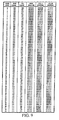
- Figure 9 presents a table showing the row selection signals and column selection signals produced by the row and column decoders 34 and 36 of Figure 6. It can be seen from Figure 9 that, whereas the row selection signals ROW 0 ⁇ 6 are thermometer-coded in the normal (conventional) manner, each set COL A0 ⁇ 6 and COL B0 ⁇ 6 of column selection signals is thermometer-coded in a modified or smoothed manner such that there is no return to zero after a full-scale value (e.g. see COL A when the input-word value changes from 7 to 8).
- thermometer coding technique In the conventional row-and-column (two dimensional) thermometer coding technique, on the other hand, only one set of normally-coded column selection signals is used and these column selection signals change from being all 1's to being all 0's whenever there is a change in the row selection signals, e.g. when the input word changes from 7 to 8. This leads to eight signals being changed (all of the column selection signals and one of the row selection signals) simultaneously, giving rise to significant coupling from the digital selection signals to the analog outputs of the cells.
- the worst-case propagation delay (as between the outputs of the input latch 32 and the control signal T of a cell) in the first embodiment corresponds to four individual gate delays.
- the row selection signal COL A4 is produced by two series-connected gates of the gate group GA1 ( Figure 7(B)), and the local decoder 26 in each cell of column 5 that is responsive to COL A4 also contains two series-connected gates 28 and 30 ( Figure 5).
- Figure 10 shows a three-dimensional array of cells for use in a DAC according to a second embodiment of the present invention.
- this embodiment there are again 64 cells in total, arranged in a 4 x 4 x 4 cubic array.
- From front to back (depth direction) there are 4 layers of square cell arrays.
- the numbers allocated to the cells in Figure 10 denote the order in the cells change their output-terminal selections as the DAC input word increases progressively.
- the local decoder 46 in Figure 11 comprises a three-input OR gate 52, a first input of which receives a first row signal r n+1 for the cell concerned.
- a second input of the OR gate 52 is connected to the output of a two-input AND gate 50 which receives at one input a second row signal r n and at the other input a first column signal c n+1 .
- the third input of the OR gate 52 is connected to the output of a three-input AND gate 48 which receives at its first input the aforementioned second row signal r n and at its second input a second column select signal c n and at its third input a depth signal d n .
- the second row signal r n is simply set permanently to logic 1 and the first row signal r n+1 is provided by a row selection signal ROW 0 corresponding to row 0 of the array.
- the second row signal r n is provided by the row selection signal ROW 0 corresponding to the preceding row 0 of the array and the first row signal r n+1 is provided by a row selection signal ROW 1 corresponding to row 1 of the array.
- ROW 2 corresponding to row 2 of the array.
- the second column signal c n is set permanently to logic 1 and the first column signal c n+1 is provided by a first-set column selection signal COL A0 if the cell is in an even row and by a second-set column selection signal COL B0 if the cell is in an odd-numbered row.
- the second column signal c n is provided by COL A0 if the cell is in an even-numbered row and by COL B0 if the cell is in an odd-numbered row.
- the first column signal c n+1 is provided by a first-set column selection signal COL A1 if the cell is in an even-numbered row and by a second-set column selection signal COL B1 if the cell is in an odd-numbered row.
- the second column signal c n is provided by COL A1 if the cell is in an even-numbered row and by COL B1 if the cell is in an odd-numbered row.
- the first column signal c n+1 is provided by a first-set column selection signal COL A2 if the cell is in an even-numbered row and by a second-set column selection signal COL B2 if the cell is in an odd-numbered row.
- the second column signal c n is provided by COL A2 if the cell is in an even-numbered row and by COL B2 if the cell is in an odd-numbered row, and the first column signal c n+1 is simply set to logic 0.
- the depth signal d n is simply set to logic 1.
- the depth signal d n is provided by a first-set depth selection signal DEP A0 if the cell is in an even-numbered column and by a second-set depth selection signal DEP B0 if the cell is in an odd-numbered column.
- the depth signal d n is provided by a first-set depth selection signal DEP A1 if the cell is in an even-numbered column and by a second-set depth selection signal DEP B1 if the cell is in an odd-numbered column.
- the depth signal d n is provided by a first-set depth selection signal DEP A2 if the cell is in an even-numbered column and by a second-set depth selection signal DEP B2 if the cell is in an odd-numbered column.
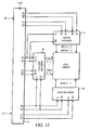
- Figure 12 shows decoder circuitry for use in producing the row, column and depth selection signals ROW 0 to ROW 2, COL A0 to COL A2, COL B0 to COL B2, DEP A0 to DEP A2 and DEP B0 to DEP B2.
- the decoder circuitry of Figure 12 includes an input latch 32 that is constructed and functions in the same way as the input latch 32 of the first embodiment ( Figure 6).
- the decoder circuitry of Figure 12 includes a depth decoder 54, a column decoder 56 and a row decoder 58.
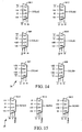
- Figure 14 shows one possible implementation of the column decoder 56 of Figure 12. Again, the column decoder in this implementation is constituted by six four-input multiplexers M7 to M12.
- Figure 15 shows one possible implementation of the row decoder 58 of Figure 12.
- the row decoder is provided by three four-input multiplexers M13 to M15.
- Each of the multiplexers M13 to M15 in Figure 15 is shown to receive at one of its three selection inputs a "format signal".
- This format signal is used to denote whether the binary input word D0 to D5 is in unsigned binary or in two's complement notation. The use of such a format signal is an optional feature.
- Figure 16 presents a table showing the ROW, COL A, COL B, DEP A, and DEP B selection signals produced by the decoders 54, 56 and 58 of Figure 12 in response to different values of the input word D5-D0.
- the maximum number of selection signals that change is two.
- none of the row selection signals ROW and none of the column selection signals COL A and COL B changes.
- thermometer coding technique used in the second embodiment is also highly efficient in terms of the total number of selection signals required: only 15 as compared with 21 in the first embodiment.
- the COL A and COL B signals undergo respective complementary changes, as do the selection signals DEP A and DEP B, the net noise level imposed on the power supply is equivalent to just three selection signals (the number of row selection signals).
- the maximum number of series-connected gates involved in the decoding process is only three in the second embodiment, contributing to high-speed operation.
- the second embodiment it is possible to produce just one set of “smoothed" column selection signals (e.g. COL A) and one set of “smoothed” depth selection signals (e.g. DEP A) instead of two sets.
- the local decoders 46 ( Figure 11) in different cells must have different logic according to whether they are in odd or even columns and whether they are in odd or even rows.
- the noise-cancellation advantage of using two sets of selection signals for the column and depth directions is lost in this case, but the number of signals requiring distribution is reduced to just nine.
- the order of the cells in the cubic array may be reversed in some columns or rows in this case, for reasons analogous to those given in relation to the first embodiment.
- thermometer coding technique i.e. coded as the row selection signals are coded in the second embodiment.
- the cells in the second embodiment could be arranged physically in three dimensions. Only a logical arrangement is required.
- the different layers in Figure 10 could be arranged side-by-side as square arrays on a common substrate.
- the cells 0 to 15 of the four row 0's could be arranged as one square array
- the cells 16 to 31 of the four row 1's could be arranged as a "row-1" array by the side of the "row-0" array on a common substrate, and so on.
- Respective "column-0", “column-1” etc. square arrays of 16 cells could also be arrayed side by side on a common substrate.
- the square arrays themselves could be subdivided in turn into lines or blocks.
- the number of rows be equal to the number of columns.
- the dimensions in the row, column and depth directions can be mutually-different.
- the coding technique embodying the present invention can produce selection signals having more than three "dimensions" (i.e. one or more further dimensions in addition to the row, column and depth directions of the second embodiment).
- thermometer coding techniques have been described above in particular relation to DACs, it will be understood that these techniques can be applied usefully in any type of circuitry in which there are a plurality of similarly-constituted circuit elements (cells) that must be activated in a sequential manner to perform respective predetermined operations.
- the coding techniques can be applied in mixers and in programmable current generators.
Landscapes
- Engineering & Computer Science (AREA)
- Theoretical Computer Science (AREA)
- Analogue/Digital Conversion (AREA)
Applications Claiming Priority (2)
| Application Number | Priority Date | Filing Date | Title |
|---|---|---|---|
| GB9800384A GB2333171A (en) | 1998-01-08 | 1998-01-08 | Thermometer coding circuitry |
| EP99300083A EP0930717A3 (en) | 1998-01-08 | 1999-01-06 | Thermometer coding circuitry |
Related Parent Applications (1)
| Application Number | Title | Priority Date | Filing Date |
|---|---|---|---|
| EP99300083A Division EP0930717A3 (en) | 1998-01-08 | 1999-01-06 | Thermometer coding circuitry |
Publications (1)
| Publication Number | Publication Date |
|---|---|
| EP1684434A1 true EP1684434A1 (en) | 2006-07-26 |
Family
ID=10825011
Family Applications (2)
| Application Number | Title | Priority Date | Filing Date |
|---|---|---|---|
| EP06008707A Withdrawn EP1684434A1 (en) | 1998-01-08 | 1999-01-06 | Thermometer coding circuitry |
| EP99300083A Withdrawn EP0930717A3 (en) | 1998-01-08 | 1999-01-06 | Thermometer coding circuitry |
Family Applications After (1)
| Application Number | Title | Priority Date | Filing Date |
|---|---|---|---|
| EP99300083A Withdrawn EP0930717A3 (en) | 1998-01-08 | 1999-01-06 | Thermometer coding circuitry |
Country Status (4)
| Country | Link |
|---|---|
| US (1) | US6163283A (https=) |
| EP (2) | EP1684434A1 (https=) |
| JP (1) | JPH11274935A (https=) |
| GB (1) | GB2333171A (https=) |
Families Citing this family (49)
| Publication number | Priority date | Publication date | Assignee | Title |
|---|---|---|---|---|
| GB2341287B (en) | 1998-09-04 | 2002-12-31 | Fujitsu Ltd | Jitter reduction |
| JP4311511B2 (ja) * | 1999-10-25 | 2009-08-12 | 日本バーブラウン株式会社 | デジタル−アナログ変換の方法および装置 |
| GB2356301B (en) | 1999-11-10 | 2003-09-10 | Fujitsu Ltd | Data multiplexing in mixed-signal circuitry |
| GB2356750B (en) * | 1999-11-24 | 2002-12-04 | Fujitsu Ltd | Reducing jitter in mixed-signal circuitry |
| US6285300B1 (en) * | 2000-02-09 | 2001-09-04 | Hewlett Packard Company | Apparatus and method for reducing power and noise through reduced switching recording in logic devices |
| US7194037B1 (en) | 2000-05-23 | 2007-03-20 | Marvell International Ltd. | Active replica transformer hybrid |
| USRE41831E1 (en) | 2000-05-23 | 2010-10-19 | Marvell International Ltd. | Class B driver |
| US7113121B1 (en) | 2000-05-23 | 2006-09-26 | Marvell International Ltd. | Communication driver |
| US7433665B1 (en) | 2000-07-31 | 2008-10-07 | Marvell International Ltd. | Apparatus and method for converting single-ended signals to a differential signal, and transceiver employing same |
| US7280060B1 (en) | 2000-05-23 | 2007-10-09 | Marvell International Ltd. | Communication driver |
| US7095348B1 (en) | 2000-05-23 | 2006-08-22 | Marvell International Ltd. | Communication driver |
| US7312739B1 (en) | 2000-05-23 | 2007-12-25 | Marvell International Ltd. | Communication driver |
| US6775529B1 (en) | 2000-07-31 | 2004-08-10 | Marvell International Ltd. | Active resistive summer for a transformer hybrid |
| SE522416C2 (sv) * | 2000-05-23 | 2004-02-10 | Ericsson Telefon Ab L M | Förfarande för scrambling av dataord och scrambler |
| US6462688B1 (en) | 2000-12-18 | 2002-10-08 | Marvell International, Ltd. | Direct drive programmable high speed power digital-to-analog converter |
| US6424283B2 (en) * | 2000-07-20 | 2002-07-23 | Texas Instruments Incorporated | Segmented high speed and high resolution digital-to-analog converter |
| US7606547B1 (en) | 2000-07-31 | 2009-10-20 | Marvell International Ltd. | Active resistance summer for a transformer hybrid |
| DE10052944C2 (de) * | 2000-10-25 | 2003-04-17 | Infineon Technologies Ag | Digital/Analog-Wandler |
| GB2373654B (en) * | 2001-03-21 | 2005-02-09 | Fujitsu Ltd | Reducing jitter in mixed-signal integrated circuit devices |
| AU2003210085A1 (en) | 2002-04-02 | 2003-10-13 | Telefonaktiebolaget L M Ericsson (Publ) | Comparator offset calibration for a/d converters |
| EP1359671A1 (en) * | 2002-05-03 | 2003-11-05 | Thomson Licensing S.A. | Thermometer code digital to analog converter for audio signals |
| KR20030086896A (ko) * | 2002-05-03 | 2003-11-12 | 톰슨 라이센싱 소시에떼 아노님 | 온도계 코드 디지털-오디오 변환기 |
| KR100454129B1 (ko) * | 2002-05-06 | 2004-10-26 | 삼성전자주식회사 | 코드 변환 장치, 디지털-아날로그 변환 장치, 그리고 지연동기 루프회로 |
| WO2004086628A1 (ja) * | 2003-03-25 | 2004-10-07 | Fujitsu Limited | エンコーダ回路及びa/d変換回路 |
| DE60313119T2 (de) | 2003-03-31 | 2007-12-20 | Ami Semiconductor Belgium Bvba | Strom DAC mit einem zweidimensionalen Matrixdecoder |
| US7889752B2 (en) * | 2003-06-05 | 2011-02-15 | Marvell International Ltd. | Dual ported network physical layer |
| DE10331545A1 (de) * | 2003-07-11 | 2005-02-10 | Infineon Technologies Ag | Digital-Analog-Wandler und Verfahren zur Digital-Analog-Wandlung |
| US8010073B2 (en) | 2004-01-22 | 2011-08-30 | Broadcom Corporation | System and method for adjusting power amplifier output power in linear dB steps |
| TWI246670B (en) * | 2004-06-08 | 2006-01-01 | Au Optronics Corp | Digital to analog converter and OLED display utilizing the same |
| US7271748B2 (en) | 2004-09-13 | 2007-09-18 | Texas Instruments Incorporated | System and method for providing a thermometer coded output filter |
| US7312662B1 (en) | 2005-08-09 | 2007-12-25 | Marvell International Ltd. | Cascode gain boosting system and method for a transmitter |
| US7577892B1 (en) | 2005-08-25 | 2009-08-18 | Marvell International Ltd | High speed iterative decoder |
| US7369076B1 (en) * | 2006-12-04 | 2008-05-06 | Taiwan Semiconductor Manufacturing Co., Ltd. | High precision DAC with thermometer coding |
| EP2026467B1 (en) * | 2007-07-30 | 2011-07-13 | ST-Ericsson SA | Current steering digital-analog converter particularly insensitive to packaging stresses |
| US8111182B2 (en) * | 2009-10-13 | 2012-02-07 | Infineon Technologies Ag | Digital to analog converter comprising mixer |
| US8766830B2 (en) | 2010-04-29 | 2014-07-01 | Agilent Technologies, Inc. | Digital waveform synthesizer for NMR phase control |
| US8604958B2 (en) * | 2011-05-13 | 2013-12-10 | Intel Mobile Communications GmbH | RF DAC with configurable DAC mixer interface and configurable mixer |
| US8847806B2 (en) * | 2012-11-29 | 2014-09-30 | Intel Mobile Communications GmbH | Digital to analog converter comprising mixer |
| US8836559B2 (en) | 2012-11-29 | 2014-09-16 | Intel Mobile Communications GmbH | Capacitive digital to analog converter |
| US9130587B2 (en) * | 2014-01-29 | 2015-09-08 | Broadcom Corporation | Frame adaptive digital to analog converter and methods for use therewith |
| US9112528B1 (en) * | 2014-01-29 | 2015-08-18 | Broadcom Corporation | Digital to analog converter with thermometer coding and methods for use therewith |
| CN105099458B (zh) * | 2014-05-09 | 2018-06-29 | 中芯国际集成电路制造(上海)有限公司 | 温度计译码器 |
| US10061341B2 (en) | 2016-09-21 | 2018-08-28 | Infineon Technologies Austria Ag | DAC controlled low power high output current source |
| US10340935B1 (en) | 2018-01-12 | 2019-07-02 | Dialog Semiconductor (Uk) Limited | Thermometer digital to analog converter |
| CN108449089A (zh) * | 2018-03-23 | 2018-08-24 | 上海唯捷创芯电子技术有限公司 | 实现数字化校准的电流舵型数模转换器、芯片及通信终端 |
| JP7099904B2 (ja) * | 2018-08-21 | 2022-07-12 | 株式会社メガチップス | デコーダ回路およびデコーダ回路の設計方法 |
| US11489534B1 (en) * | 2021-10-11 | 2022-11-01 | Cirrus Logic, Inc. | Digital-to-analog conversion architecture and method |
| US12015510B2 (en) | 2022-05-27 | 2024-06-18 | International Business Machines Corporation | Transmitter with uniform driver segment activity |
| US12587208B2 (en) * | 2022-06-17 | 2026-03-24 | Apple Inc. | Digital-to-analog converter with dynamic alternating fill order systems and methods |
Citations (5)
| Publication number | Priority date | Publication date | Assignee | Title |
|---|---|---|---|---|
| US4503421A (en) * | 1981-05-27 | 1985-03-05 | Nippon Electric Co., Ltd. | Digital to analog converter |
| GB2223369A (en) * | 1988-08-18 | 1990-04-04 | Plessey Co Plc | Analogue-to-digital converters |
| JPH0548460A (ja) * | 1991-06-05 | 1993-02-26 | Matsushita Electric Ind Co Ltd | A/d変換器とこれを用いたセンサ及び3次元集積回路 |
| US5303200A (en) * | 1992-07-02 | 1994-04-12 | The Boeing Company | N-dimensional multi-port memory |
| US5539405A (en) * | 1993-07-29 | 1996-07-23 | Cirrus Logic, Inc. | DAC achieving monotonicity with equal sources and shift array therefor |
Family Cites Families (7)
| Publication number | Priority date | Publication date | Assignee | Title |
|---|---|---|---|---|
| US4870417A (en) * | 1988-02-12 | 1989-09-26 | North American Philips Corporation, Signetics Division | Error correction circuit suitable for thermometer or circular code |
| KR930009431B1 (ko) * | 1991-12-31 | 1993-10-04 | 현대전자산업주식회사 | 2차원 대칭적 온도계형 매트릭스 디코더의 디지탈/아날로그 변환기 |
| US5844515A (en) * | 1994-11-04 | 1998-12-01 | Lg Semicon Co., Ltd | Digital to analog converter and bias circuit therefor |
| US5633636A (en) * | 1995-10-02 | 1997-05-27 | Analog Devices, Inc. | Half-gray digital encoding method and circuitry |
| KR100218329B1 (ko) * | 1996-11-08 | 1999-09-01 | 구본준 | 고속 저전력 디지탈 아날로그 컨버터 |
| US5977899A (en) * | 1997-09-25 | 1999-11-02 | Analog Devices, Inc. | Digital-to-analog converter using noise-shaped segmentation |
| US5955980A (en) * | 1997-10-03 | 1999-09-21 | Motorola, Inc. | Circuit and method for calibrating a digital-to-analog converter |
-
1998
- 1998-01-08 GB GB9800384A patent/GB2333171A/en not_active Withdrawn
-
1999
- 1999-01-06 EP EP06008707A patent/EP1684434A1/en not_active Withdrawn
- 1999-01-06 EP EP99300083A patent/EP0930717A3/en not_active Withdrawn
- 1999-01-08 JP JP11003205A patent/JPH11274935A/ja active Pending
- 1999-01-08 US US09/227,200 patent/US6163283A/en not_active Expired - Lifetime
Patent Citations (5)
| Publication number | Priority date | Publication date | Assignee | Title |
|---|---|---|---|---|
| US4503421A (en) * | 1981-05-27 | 1985-03-05 | Nippon Electric Co., Ltd. | Digital to analog converter |
| GB2223369A (en) * | 1988-08-18 | 1990-04-04 | Plessey Co Plc | Analogue-to-digital converters |
| JPH0548460A (ja) * | 1991-06-05 | 1993-02-26 | Matsushita Electric Ind Co Ltd | A/d変換器とこれを用いたセンサ及び3次元集積回路 |
| US5303200A (en) * | 1992-07-02 | 1994-04-12 | The Boeing Company | N-dimensional multi-port memory |
| US5539405A (en) * | 1993-07-29 | 1996-07-23 | Cirrus Logic, Inc. | DAC achieving monotonicity with equal sources and shift array therefor |
Non-Patent Citations (1)
| Title |
|---|
| PATENT ABSTRACTS OF JAPAN vol. 017, no. 347 (E - 1391) 30 June 1993 (1993-06-30) * |
Also Published As
| Publication number | Publication date |
|---|---|
| US6163283A (en) | 2000-12-19 |
| EP0930717A2 (en) | 1999-07-21 |
| GB2333171A (en) | 1999-07-14 |
| JPH11274935A (ja) | 1999-10-08 |
| EP0930717A3 (en) | 2003-01-02 |
| GB9800384D0 (en) | 1998-03-04 |
Similar Documents
| Publication | Publication Date | Title |
|---|---|---|
| US6163283A (en) | Thermometer coding circuitry | |
| JPH11274935A5 (https=) | ||
| US5389843A (en) | Simplified structure for programmable delays | |
| US4825401A (en) | Functional dividable multiplier array circuit for multiplication of full words or simultaneous multiplication of two half words | |
| US8830102B2 (en) | Compact digital-to-analog converter | |
| US4825105A (en) | Circuit for generation of logic variables, using multiplexes and inverters | |
| JP2008187748A (ja) | セルアレイ回路 | |
| JP2002100991A (ja) | D/aコンバータ | |
| US4910514A (en) | D/A converter | |
| US6542104B1 (en) | Method and apparatus for low power thermometer to binary coder | |
| CN111106832B (zh) | Dac电路结构和电阻分压式dac | |
| EP0330367A2 (en) | Digital to analogue convertors | |
| US5162800A (en) | Digital-to-analog converting unit with improved linearity | |
| US4408184A (en) | Keyboard switch circuit | |
| Blair | Low cost sorting circuit for VLSI | |
| US5189320A (en) | Programmable logic device with multiple shared logic arrays | |
| KR20160105654A (ko) | 신호 조합 회로 및 이를 이용한 디지털-아날로그 변환 회로 | |
| US6617986B2 (en) | Area efficient, sequential gray code to thermometer code decoder | |
| JP3339566B2 (ja) | サーモメトリック−バイナリコード変換方法および回路、それに使用されるエンコーダ素子回路 | |
| KR100520591B1 (ko) | 가산회로및그레이아웃구조 | |
| US4411009A (en) | Digital dual half word or single word position scaler | |
| US7068978B2 (en) | Current cell type digital-to-analog converter | |
| Baranwal et al. | Design and analysis of 8 bit fully segmented digital to analog converter | |
| JPH04218829A (ja) | パリティビットジェネレータを備えるバレルシフタ | |
| KR19990086692A (ko) | 플래쉬 방식 아날로그/디지털 변환장치 |
Legal Events
| Date | Code | Title | Description |
|---|---|---|---|
| PUAI | Public reference made under article 153(3) epc to a published international application that has entered the european phase |
Free format text: ORIGINAL CODE: 0009012 |
|
| AC | Divisional application: reference to earlier application |
Ref document number: 0930717 Country of ref document: EP Kind code of ref document: P |
|
| AK | Designated contracting states |
Kind code of ref document: A1 Designated state(s): AT BE CH CY DE DK ES FI FR GB GR IE IT LI LU MC NL PT SE |
|
| RIN1 | Information on inventor provided before grant (corrected) |
Inventor name: SCHOFIELD, WILLIAM GEORGE JOHN |
|
| AKX | Designation fees paid | ||
| REG | Reference to a national code |
Ref country code: DE Ref legal event code: 8566 |
|
| STAA | Information on the status of an ep patent application or granted ep patent |
Free format text: STATUS: THE APPLICATION IS DEEMED TO BE WITHDRAWN |
|
| 18D | Application deemed to be withdrawn |
Effective date: 20070127 |