EP1683398B2 - Thermischer schutz für lampenballastschaltungen - Google Patents
Thermischer schutz für lampenballastschaltungen Download PDFInfo
- Publication number
- EP1683398B2 EP1683398B2 EP04801048.2A EP04801048A EP1683398B2 EP 1683398 B2 EP1683398 B2 EP 1683398B2 EP 04801048 A EP04801048 A EP 04801048A EP 1683398 B2 EP1683398 B2 EP 1683398B2
- Authority
- EP
- European Patent Office
- Prior art keywords
- ballast
- temperature
- signal
- output current
- circuit
- Prior art date
- Legal status (The legal status is an assumption and is not a legal conclusion. Google has not performed a legal analysis and makes no representation as to the accuracy of the status listed.)
- Expired - Lifetime
Links
Images


Classifications
-
- H—ELECTRICITY
- H05—ELECTRIC TECHNIQUES NOT OTHERWISE PROVIDED FOR
- H05B—ELECTRIC HEATING; ELECTRIC LIGHT SOURCES NOT OTHERWISE PROVIDED FOR; CIRCUIT ARRANGEMENTS FOR ELECTRIC LIGHT SOURCES, IN GENERAL
- H05B41/00—Circuit arrangements or apparatus for igniting or operating discharge lamps
- H05B41/14—Circuit arrangements
- H05B41/26—Circuit arrangements in which the lamp is fed by power derived from DC by means of a converter, e.g. by high-voltage DC
- H05B41/28—Circuit arrangements in which the lamp is fed by power derived from DC by means of a converter, e.g. by high-voltage DC using static converters
- H05B41/282—Circuit arrangements in which the lamp is fed by power derived from DC by means of a converter, e.g. by high-voltage DC using static converters with semiconductor devices
- H05B41/285—Arrangements for protecting lamps or circuits against abnormal operating conditions
-
- H—ELECTRICITY
- H05—ELECTRIC TECHNIQUES NOT OTHERWISE PROVIDED FOR
- H05B—ELECTRIC HEATING; ELECTRIC LIGHT SOURCES NOT OTHERWISE PROVIDED FOR; CIRCUIT ARRANGEMENTS FOR ELECTRIC LIGHT SOURCES, IN GENERAL
- H05B41/00—Circuit arrangements or apparatus for igniting or operating discharge lamps
- H05B41/14—Circuit arrangements
- H05B41/36—Controlling
- H05B41/38—Controlling the intensity of light
- H05B41/39—Controlling the intensity of light continuously
- H05B41/392—Controlling the intensity of light continuously using semiconductor devices, e.g. thyristor
- H05B41/3921—Controlling the intensity of light continuously using semiconductor devices, e.g. thyristor with possibility of light intensity variations
- H05B41/3925—Controlling the intensity of light continuously using semiconductor devices, e.g. thyristor with possibility of light intensity variations by frequency variation
-
- G—PHYSICS
- G05—CONTROLLING; REGULATING
- G05F—SYSTEMS FOR REGULATING ELECTRIC OR MAGNETIC VARIABLES
- G05F1/00—Automatic systems in which deviations of an electric quantity from one or more predetermined values are detected at the output of the system and fed back to a device within the system to restore the detected quantity to its predetermined value or values, i.e. retroactive systems
-
- H—ELECTRICITY
- H01—ELECTRIC ELEMENTS
- H01H—ELECTRIC SWITCHES; RELAYS; SELECTORS; EMERGENCY PROTECTIVE DEVICES
- H01H5/00—Snap-action arrangements, i.e. in which during a single opening operation or a single closing operation energy is first stored and then released to produce or assist the contact movement
- H01H5/04—Energy stored by deformation of elastic members
-
- H—ELECTRICITY
- H05—ELECTRIC TECHNIQUES NOT OTHERWISE PROVIDED FOR
- H05B—ELECTRIC HEATING; ELECTRIC LIGHT SOURCES NOT OTHERWISE PROVIDED FOR; CIRCUIT ARRANGEMENTS FOR ELECTRIC LIGHT SOURCES, IN GENERAL
- H05B41/00—Circuit arrangements or apparatus for igniting or operating discharge lamps
- H05B41/14—Circuit arrangements
- H05B41/26—Circuit arrangements in which the lamp is fed by power derived from DC by means of a converter, e.g. by high-voltage DC
- H05B41/28—Circuit arrangements in which the lamp is fed by power derived from DC by means of a converter, e.g. by high-voltage DC using static converters
- H05B41/282—Circuit arrangements in which the lamp is fed by power derived from DC by means of a converter, e.g. by high-voltage DC using static converters with semiconductor devices
- H05B41/285—Arrangements for protecting lamps or circuits against abnormal operating conditions
- H05B41/2851—Arrangements for protecting lamps or circuits against abnormal operating conditions for protecting the circuit against abnormal operating conditions
- H05B41/2856—Arrangements for protecting lamps or circuits against abnormal operating conditions for protecting the circuit against abnormal operating conditions against internal abnormal circuit conditions
-
- H—ELECTRICITY
- H05—ELECTRIC TECHNIQUES NOT OTHERWISE PROVIDED FOR
- H05B—ELECTRIC HEATING; ELECTRIC LIGHT SOURCES NOT OTHERWISE PROVIDED FOR; CIRCUIT ARRANGEMENTS FOR ELECTRIC LIGHT SOURCES, IN GENERAL
- H05B41/00—Circuit arrangements or apparatus for igniting or operating discharge lamps
- H05B41/14—Circuit arrangements
- H05B41/26—Circuit arrangements in which the lamp is fed by power derived from DC by means of a converter, e.g. by high-voltage DC
- H05B41/28—Circuit arrangements in which the lamp is fed by power derived from DC by means of a converter, e.g. by high-voltage DC using static converters
- H05B41/295—Circuit arrangements in which the lamp is fed by power derived from DC by means of a converter, e.g. by high-voltage DC using static converters with semiconductor devices and specially adapted for lamps with preheating electrodes, e.g. for fluorescent lamps
- H05B41/298—Arrangements for protecting lamps or circuits against abnormal operating conditions
- H05B41/2981—Arrangements for protecting lamps or circuits against abnormal operating conditions for protecting the circuit against abnormal operating conditions
- H05B41/2986—Arrangements for protecting lamps or circuits against abnormal operating conditions for protecting the circuit against abnormal operating conditions against internal abnormal circuit conditions
Definitions
- This invention relates to thermal protection for lamp ballasts. Specifically, this invention relates to a ballast having active thermal management and protection circuitry that allows the ballast to safely operate when a ballast over-temperature condition has been detected, allowing the ballast to safely continue to provide power to the lamp.
- Lamp ballasts are devices that convert standard line voltage and frequency to a voltage and frequency suitable for a specific lamp type.
- ballasts are one component of a lighting fixture that receives one or more fluorescent lamps.
- the lighting fixture may have more than one ballast.
- Ballasts are generally designed to operate within a specified operating temperature.
- the maximum operating temperature of the ballast can be exceeded as the result of a number of factors, including improper matching of the ballast to the lamp(s), improper heat sinking, and inadequate ventilation of the lighting fixture. If an over-temperature condition is not remedied, then the ballast and/or lamp(s) may be damaged or destroyed.
- ballasts have circuitry that shuts down the ballast upon detecting an over-temperature condition. This is typically done by means of a thermal cut-out switch that senses the ballast temperature. When the switch detects an over-temperature condition, it shuts down the ballast by removing its supply voltage. If a normal ballast temperature is subsequently achieved, the switch may restore the supply voltage to the ballast. The result is lamp flickering and/or a prolonged loss of lighting. The flickering and loss of lighting can be annoying. In addition, the cause may not be apparent and might be mistaken for malfunctions in other electrical systems, such as the lighting control switches, circuit breakers, or even the wiring.
- US 6,621,239 discloses a method and apparatus for controlling the temperature of a multi-parameter light.
- DE 100 13 041 discloses a method of operating a light with a fluorescent lamp which involves setting a manufacturer's rated loading for a detected lamp type in normal operation and reducing/removing the load if a critical temperature is reached/exceeded.
- US 6,198,234 discloses a dimmable, backlight system for providing increased light output at low temperatures and which provides a full range of dimming.
- US 2003/031037 discloses a converter for converting an AC power main voltage to a voltage suitable for driving a lamp.
- DE 198 05 801 discloses a lamp control circuit for high pressure gas discharge lamps such as, for example, sodium, mercury, halogen and metal vapor lamps.
- DE 195 36 142 discloses a thermally-protected control apparatus containing electrical components, in particular for controlling high-pressure gas-discharge lamps in motor vehicle headlights.
- US 6,452,344 discloses an electronic dimming ballast which has a parallel loaded resonant output circuit plus a combination of pulse width modulation and frequency variation for use in the dimming of compact fluorescent lamps.
- US 5,869,969 discloses a temperature compensation module for use with battery charger/rectifier units.
- a circuit for controlling the output current from a ballast to a lamp comprising:
- a method of controlling the output current from a ballast to a lamp comprising the steps of:
- a lamp ballast has temperature sensing circuitry and control circuitry responsive to the temperature sensor that limits the output current provided by the ballast when an over-temperature condition has been detected.
- the control circuitry actively adjusts the output current as long as the over-temperature condition is detected so as to attempt to restore an acceptable operating temperature while continuing to operate the ballast (i.e., without shutting down the ballast).
- the output current is maintained at a reduced level until the sensed temperature returns to the acceptable temperature.
- linear and step function adjustments to output current are employed in differing combinations.
- the linear function may be replaced with any continuous decreasing function including linear and non-linear functions, Gradual, linear adjustment of the output current tends to provide a relatively imperceptible change in lighting intensity to a casual observer, whereas a stepwise adjustment may be used to create an obvious change so as to alert persons that a problem has been encountered and/or corrected.
- the invention has particular application to (but is not limited to) dimming ballasts of the type that are responsive to a dimming control to dim fluorescent lamps connected to the ballast.
- adjustment of the dimming control alters the output current delivered by the ballast. This is carried out by altering the duty cycle, frequency or pulse width of switching signals delivered to one or more switching transistors in the output circuit of the ballast
- These switching transistors may also be referred to as output switches.
- An output switch is a switch, such as a transistor, whose duty cycle and/or switching frequency is varied to control the output current of the ballast.
- a tank in the ballast's output circuit receives the output of the switches to provide a generally sinusoidal (AC) output voltage and current to the lamp(s).
- the duty cycle, frequency or pulse width is controlled by a control circuit that is responsive to the output of a phase to DC converter that receives a phase controlled AC dimming signal provided by the dimming control.
- the output of the phase to DC converter is a DC signal having a magnitude that varies in accordance with a duty cycle value of the dimming Signal.
- a pair of voltage clamps (high and low end clamps) is disposed in the phase to DC converter for the purpose of establishing high end and low end intensity levels. The low end clamp sets the minimum output current level of the ballast, while the high end clamp sets its maximum output current level.
- a ballast temperature sensor is coupled to a foldback protection circuit that dynamically adjusts the high end clamping voltage in accordance with the sensed ballast temperature when the sensed ballast temperature exceeds a threshold.
- the amount by which the high end clamping voltage is adjusted depends upon the difference between the sensed ballast temperature and the threshold.
- the high and low end clamps need not be employed to implement the invention.
- the foldback protection circuit may communicate with a multiplier, that in turn communicates with the control circuit.
- the control circuit is responsive to the output of the multiplier to adjust the duty cycle, pulse width or frequency of the switching signal.
- the invention may also be employed in connection with a non-dimming ballast in accordance with the foregoing.
- a ballast temperature sensor and foldback protection are provided as above described, and the foldback protection circuit communicates with the control circuit to alter the duty cycle, pulse width or frequency of the one or more switching signals when the ballast temperature exceeds the threshold.
- a temperature cutoff switch may also be employed to remove the supply voltage to shut down the ballast completely (as in the prior art) if the ballast temperature exceeds a maximum temperature threshold.
- a typical non-dimming ballast includes a front end AC to DC converter 102 that converts applied line voltage 100a, b, typically 120 volts AC, 60 Hz, to a higher voltage, typically 400 to 500 volts DC.
- Capacitor 104 stabilizes the high voltage output on 103a, b of AC to DC converter 102.
- the high voltage across capacitor 104 is presented to a back end DC to AC converter 106, which typically produces a 100 to 400 Volt AC output at 45 KHz to 80 KHz at terminals 107a, b to drive the load 108, typically one or more fluorescent lamps.
- the ballast typically includes a thermal cut-out switch 110. Upon detecting an over-temperature condition, the thermal cutout switch 110 removes the supply voltage at 100a to shut down the ballast. The supply voltage is restored if the switch detects that the ballast returns to a normal or acceptable temperature.
- Figure 2 shows additional details of the back end DC to AC converter 106, and includes circuitry 218, 220 and 222 that permits the ballast to respond to a dimming signal 217 from a dimming control 216.
- the dimming control 216 may be any phase controlled dimming device and may be wall mountable.
- An example of a commercially available dimming ballast of the type of Figure 2 is model number FDB T554-120-2, available from Lutron Electronics, Co., Inc., Coopersburg, PA, the assignee of the present invention.
- the dimming signal is a phase controlled AC dimming signal, of the type shown in Figure 4a , such that the duty cycle of the dimming signal and hence the RMS voltage of the dimming signal varies with adjustment of the dimming actuator.
- Dimming signal 217 drives a phase to DC converter 218 that converts the phase controlled dimming signal 217 to a DC voltage signal 219 having a magnitude that varies in accordance with a duty cycle value of the dimming signal, as graphically shown in Figure 4b . It will be seen that the signal 219 generally linearly tracks the dimming signal 217. However, clamping circuit 220 modifies this generally linear relationship as described hereinbelow.
- the signal 219 stimulates ballast drive circuit 222 to generate at least one switching control signal 223a, b.
- the switching control signals 223a, b shown in Figure 2 are typical of those in the art that drive output switches in an inverter function (DC to AC) in the back-end converter 106.
- An output switch is a switch whose duty cycle and/or switching frequency is varied to control the output current of the ballast.
- the switching control signals control the opening and closing of output switches 210, 211 coupled to a tank circuit 212, 213.
- Figure 2 depicts a pair of switching control signals, 223a, b, an equivalent function that uses only one switching signal may be used.
- a current sense device 228 provides an output (load) current feedback signal 226 to the ballast drive circuit 222.
- the duty cycle, pulse width or frequency of the switching control signals is varied in accordance with the level of the signal 219 (subject to clamping by the circuit 220), and the feedback signal 226, to determine the output voltage and current delivered by the ballast
- High and low end clamp circuit 220 in the phase to DC converter limits the output 219 of the phase to DC converter.
- the effect of the high and low end clamp circuit 220 on the phase to DC converter is graphically shown in the Figure 4c . It will be seen that the high and low end clamp circuit 220 clamps the upper and lower ends of the otherwise linear signal 219 at levels 400 and 401, respectively. Thus, the high and low end clamp circuitry 220 establishes minimum and maximum dimming levels.
- a temperature cutoff switch 110 ( Figure 1 ) is also usually employed. All that has been described thus far is prior art.
- FIG 3 is a block diagram of a dimming ballast employing the present invention.
- the dimming ballast of Figure 2 is modified to include a ballast temperature sensing circuit 300 that provides a ballast temperature signal 305 to a foldback protection circuit 310.
- the foldback protection circuit 310 provides an appropriate adjustment signal 315 to the high and low end clamp circuit 220' to adjust the high cutoff level 400.
- clamp circuit 220' is similar to clamp circuit 220 of Figure 2 , however, the clamp circuit 220' is further responsive to adjustment signal 315, which dynamically adjusts the high end clamp voltage (i.e. level 400).
- the ballast temperature sensing circuit 300 may comprise one or more thermistors with a defined resistance to temperature coefficient characteristic, or another type of temperature sensing thermostat device or circuit.
- Foldback protection circuit 310 generates an adjustment signal 315 in response to comparison of temperature signal 305 to a threshold.
- the foldback protection circuit may provide either a linear output (using a linear response generator) or a step function output (using a step response generator), or a combination of both, if the comparison determines that an over-temperature condition exists.
- the exemplar linear function output by the foldback protection circuit shown in Figure 3 may be replaced with any continuous function including linear and non-linear functions. For the purpose of simplicity and clarity, the linear continuous function example will be used. But, it can be appreciated that other continuous functions may equivalently be used.
- the high end clamp level 400 is reduced from its normal operating level when the foldback protection circuit 310 indicates that an over-temperature condition exists. Reducing the high end clamp level 400 adjusts the drive signal 219' to the ballast drive circuit 222 so as to alter the duty cycle, pulse width or frequency of the switching control signals 223a, b and hence reduce the output current provided by the ballast to load 108. Reducing output current should, under normal circumstances, reduce the ballast temperature. Any decrease in ballast temperature is reflected in signal 315, and the high end clamp level 400 is increased and/or restored to normal, accordingly.
- FIGS. 5a - 5d graphically illustrate various examples of adjusting the output current during an over-temperature condition. These examples are not exhaustive and other functions or combinations of functions may be employed.
- output current is adjusted linearly when the ballast temperature exceeds threshold T1
- the foldback protection circuit 310 provides a limiting input to the high end clamp portion of the clamp circuit 220'so as to linearly reduce the high end clamp level 400, such that the output current may be reduced linearly from 100% to a preselected minimum.
- the temperature T1 may be preset by selecting the appropriate thresholds in the foldback protection circuit 310 as described in greater detail below.
- the output current can be dynamically adjusted in the linear region 510 until the ballast temperature stabilizes and is permitted to be restored to normal.
- the linear adjustment of the output current may be such that the resulting change in intensity is relatively imperceptible to a casual observer. For example, a 40% reduction in output current (when the lamp is saturated) may produce only a 10% reduction in perceived intensity.
- the embodiment of the invention of Figure 3 limits the output current of the load to the linear region 510 even if the output current is less than the maximum (100%) value.
- the dimming control signal 217 may be set to operate the lamp load 108 at, for example, 80% of the maximum load current. If the temperature rises to above a temperature value T1, a linear limiting response is not activated until the temperature reaches a value of T1*. At that value, linear current limiting may occur which will limit the output current to the linear region 510. This allows the maximum (100%) linear limiting profile to be utilized even if the original setting of the lamp was less than 100% load current. As the current limiting action of the invention allows the temperature to fall, the lamp load current will once again return to the originally set 80% level as long as the dimmer control signal 217 is unchanged.
- output current may be reduced according to a step function when the ballast temperature exceeds threshold T2. If the ballast temperature exceeds T2, then the foldback protection circuit 310 provides a limiting input to the high end portion of the clamp 220' so as to step down the high end clamp level 400; this results in an immediate step down in supplied output current from 100% to level L1. Once the ballast temperature returns to an acceptable operating temperature T3, the foldback protection circuit 310 allows the output current to immediately return to 100%, again according to a step function. Notice that recovery temperature T3 is lower than T2. Thus, the foldback-protection circuit 310 exhibits hysteresis. The use of hysteresis helps to prevent oscillation about T2 when the ballast is recovering from a higher temperature. The abrupt changes in output current may result in obvious changes in light intensity so as to alert persons that a problem has been encountered and/or corrected.
- both linear and step function adjustments in output current are employed.
- T5 the ballast temperature exceeds T5
- the ballast temperature returns to an acceptable operating temperature T6
- the foldback protection circuit 310 allows the output current to return to level L4, again according to a step function, and the output current is again dynamically adjusted in a linear manner.
- recovery temperature T6 is lower than T5.
- the foldback protection circuit 310 exhibits hysteresis, again preventing oscillation about T5.
- the linear adjustment of the output current between 100% and L2 may be such that the resulting change in lamp intensity is relatively imperceptible to a casual observer, whereas the abrupt changes in output current between L2 and L3 may be such that they result in obvious changes in light intensity so as to alert persons that a problem has been encountered and/or corrected.
- a series of step functions is employed to adjust the output current between temperatures T7 and T8. Particularly, there is a step-wise decrease in output current from 100% to level L5 at T7 and another step-wise decrease in output current from level L5 to level L6 at T8. Upon a temperature decrease and recovery, there is a step-wise increase in output current from level L6 to level L5 at T11, and another step-wise increase in output current from level L5 to 100% at T12 (each step function thus employing hysteresis to prevent oscillation about T7 and T8). Between ballast temperatures of T9 and T10, however, linear adjustment of the output current, between levels L6 and L7, is employed.
- step and linear response generators in the foldback protection circuitry 310 of Figure 3 allow the setting of thresholds for the various temperature settings.
- One or more of the step-wise adjustments in output current may result in obvious changes in light intensity, whereas the linear adjustment may be relatively imperceptible.
- a thermal cutout switch may be employed, as illustrated at 110 in Figure 1 , to remove the supply voltage and shut down the ballast if a substantial over-temperature condition is detected.
- FIG. 6 illustrates one circuit level implementation of selected portions of the Figure 3 embodiment.
- the foldback protection circuit 310 includes a linear response generator 610 and a step response generator 620.
- the adjustment signal 315 drives the output stage 660 of the phase to DC converter 218' via the high end clamp 630 of the clamp circuit 220'.
- a low end clamp 640 is also shown.
- Temperature sensing circuit 300 may be an integrated circuit device that exhibits an increasing voltage output with increasing temperature.
- the temperature sensing circuit 300 feeds the linear response generator 610 and the step response generator 620.
- the step response generator 620 is in parallel with the linear response generator 610 and both act in a temperature dependent manner to produce the adjustment signal 315.
- the temperature threshold of the linear response generator 610 is set by voltage divider R3, R4, and the temperature threshold of the step response generator 620 is set by voltage divider R1, R2.
- the hysteresis characteristic of the step response generator 620 is achieved by means of feedback, as is well known in the art.
- the threshold of low end clamp 640 is set via a voltage divider labeled simply VDIV1.
- the phase controlled dimming signal 217 is provided to one input of a comparator 650.
- the other input of comparator 650 receives a voltage from a voltage divider labeled VDIV2.
- the output stage 660 of the phase to DC converter 218' provides the control signal 219'.
- the temperature thresholds of the linear and step response generators 610, 620 may be set such that the foldback protection circuit 310 exhibits either a linear function followed by a step function (See Figure 5c ), or the reverse. Sequential step functions may be achieved by utilizing two step response generators 620 (See steps L5 and L6 of Figure 5d ). Likewise, sequential linear responses may be achieved by replacing the step response generator 620 with another linear response generator 610. If only a linear function ( Figure 5a ) or only a step function ( Figure 5b ) is desired, only the appropriate response generator is employed.
- the foldback protection circuit 310 may be designed to produce more than two types of functions, e.g., with the addition of another parallel stage. For example the function of Figure 5d may be obtained with the introduction of another step response generator 620 to the foldback protection circuit, and by setting the proper temperature thresholds.
- FIG. 7 is a block diagram of a dimming ballast according to another embodiment of the invention.
- the dimming ballast of Figure 2 is modified to include a ballast temperature sensing circuit 300 that provides a ballast temperature signal 305 to a foldback protection circuit 310.
- the foldback protection circuit 310' produces, as before, an adjustment signal 315' to modify the response of the DC to AC back end 106 in an over-temperature condition.
- the phase controlled dimming signal 217 from the dimming control 216, and the output of the high and low end clamps 220 act to produce the control signal 219 that is used, for example, in the dimming ballast of Figure 2 .
- ballast drive circuit 222' performs the same function as the ballast drive circuit 222 of Figure 3 except that ballast drive circuit 222' may have a differently scaled input as described hereinbelow.
- dimming control 216 acts to deliver a phase controlled dimming signal 217 to the phase to DC converter 218.
- the phase to DC converter 218 provides an input 219 to the multiplier 700.
- the other multiplier input is the adjustment signal 315'.
- the multiplier 700 is influenced only by the signal 219 because the adjustment signal 315' is scaled to represent a multiplier of 1.0.
- adjustment signal 315" is similar to 315 of Figure 3 except for the effect of scaling.
- the foldback protection circuit 310' scales the adjustment signal 315' to represent a multiplier of less than 1.0. The product of the multiplication of the signal 219 and the adjustment signal 315' will therefore be less than 1.0 and will thus scale back the drive signal 701, thus decreasing the output current to load 108.
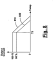
- Figure 8 illustrates the response of output current versus temperature for the embodiment of Figure 7 .
- the current limiting function may be linearly decreasing beyond a temperature T1.
- the response of the embodiment of Figure 7 at lower initial current settings is more immediate.
- current limiting begins once the threshold temperature of T1 is reached.
- the operating current of the lamp 108 may be set to be at a level lower than maximum, say at 80%, via dimmer control signal 217 which results in an input signal 219 to multiplier 700.
- the multiplier input signal 315' would immediately begin to decrease to a level below 1.0 thus producing a reduced output for the drive signal 701. Therefore, the 100% current limiting response profile 810 is different from the 80% current limiting response profile 820 beyond threshold temperature T1.
- the multiplier 700 may be implemented as either an analog or a digital multiplier. Accordingly, the drive signals for the multiplier input would be correspondingly analog or digital in nature to accommodate the type of multiplier 700 utilized.
- FIG 9 illustrates application of the invention to a non-dimming ballast, e.g., of the type of Figure 2 , which does not employ high end and low end clamp circuitry or a phase to DC converter.
- a ballast temperature sensing circuit 300 that provides a ballast temperature signal 305 to a foldback protection circuit 310".
- the foldback protection circuit 310' provides an adjustment signal 315" to ballast drive circuit 222. Instead of adjusting the level of a high end clamp, the adjustment signal 315" is provided directly to ballast drive circuit 222. Otherwise the foregoing description of the function and operation of Figure 3 , and the examples of Figures 5a - 5d , are applicable.
- circuitry described herein for implementing the invention is preferably packaged with, or encapsulated within, the ballast itself, although such circuitry could be separately packaged from, or remote from, the ballast.
Landscapes
- Engineering & Computer Science (AREA)
- Physics & Mathematics (AREA)
- Electromagnetism (AREA)
- General Physics & Mathematics (AREA)
- Radar, Positioning & Navigation (AREA)
- Automation & Control Theory (AREA)
- Circuit Arrangements For Discharge Lamps (AREA)
- Discharge-Lamp Control Circuits And Pulse- Feed Circuits (AREA)
Claims (28)
- Stromkreis zum Steuern des Ausgangsstroms von einem Vorschaltgerät zu einer Lampe (108), wobei der Stromkreis Folgendes umfasst:a) einen Temperatursensor-Stromkreis (300), der dazu angepasst ist, thermisch an das Vorschaltgerät gekoppelt zu sein und ein Temperatursignal (305) mit einer für die Vorschaltgerätetemperatur Tb indikativen Größe bereitzustellen; undb) Steuerschaltungen (218', 220', 222), die dazu angepasst sind, das Vorschaltgerät zu veranlassen, in einen Strombegrenzungsmodus zu wechseln, während das Vorschaltgerät weiter betrieben wird, indem der Ausgangsstrom reduziert wird, wenn die Größe des Temperatursignals (305) angibt, dass Tb eine vorherbestimmte maximale erwünschte Vorschaltgerätetemperatur T1 überschritten hat,
dadurch gekennzeichnet, dass
die Steuerschaltungen dazu angepasst sind, den Ausgangsstrom in dem Strombegrenzungsmodus gemäß in jeweiligen Temperaturbereichen definierten Stufenfunktionen und stetigen Funktionen zu reduzieren, wobei die stufenweisen Stromreduktionen so abrupt sind, dass sie zu für Menschen wahrnehmbaren Lichtintensitätsänderungen führen und damit Personen darauf aufmerksam machen, dass ein Übertemperaturzustand eingetreten ist. - Stromkreis nach Anspruch 1, wobei es sich bei der stetigen Funktion um eine lineare Funktion handelt.
- Stromkreis nach Anspruch 1, wobei die Steuerschaltungen (218', 220', 222) beim Betreiben des Vorschaltgeräts im Strombegrenzungsmodus auf eine Bestimmung reagieren, dass Tb gleich oder geringer ist als eine Schwellentemperatur T3, um den Ausgangsstrom zu erhöhen, wobei T3 geringer ist als T1, so dass das Ausgangsstromprofil im Strombegrenzungsmodus eine Hysterese aufweist.
- Stromkreis nach Anspruch 3, umfassend Schaltungen, die dazu angepasst sind, ein erstes Schwellenwertsignal mit einer für T1 indikativen Größe und mindestens ein weiteres zweites Schwellenwertsignal mit einer für T3 indikativen Größe bereitzustellen.
- Stromkreis nach Anspruch 3, wobei die Steuerschaltungen (218', 220', 222) dazu angepasst sind, den Ausgangsstrom gemäß einer stufenweisen Verstellung zu erhöhen, wenn Tb gleich oder geringer als die Schwellentemperatur T3 ist.
- Stromkreis nach Anspruch 1, wobei der Strombegrenzungsmodus einen ersten Zustand und einen zweiten Zustand umfasst, wobei im ersten Zustand der Ausgangsstrom gemäß einer linearen Funktion in einem ersten Temperaturbereich reduziert wird und im zweiten Zustand der Ausgangsstrom gemäß einer stufenweisen Verstellung in einem zweiten Temperaturbereich weiter reduziert wird.
- Stromkreis nach Anspruch 6, wobei die Steuerschaltungen (218', 220', 222) dazu angepasst sind, das Vorschaltgerät zu veranlassen, in den ersten Zustand des Strombegrenzungsmodus zu wechseln, wenn die Größe des Temperatursignals (305) angibt, dass Tb T1 überschritten hat, und in den zweiten Zustand zu wechseln, wenn die Größe des Temperatursignals angibt, dass Tb eine Temperatur T2, die größer ist als T1, überschritten hat.
- Stromkreis nach Anspruch 7, wobei die Steuerschaltungen (218', 220', 222), beim Betreiben des Vorschaltgeräts im zweiten Zustand des Strombegrenzungsmodus auf eine Bestimmung reagieren, dass Tb auf eine Temperatur T3 gesunken ist, wobei T3 zwischen T1 und T2 liegt, um den Ausgangsstrom gemäß einer stufenweisen Verstellung zu erhöhen.
- Stromkreis nach Anspruch 1, wobei der Strombegrenzungsmodus einen ersten Zustand umfasst, wobei im ersten Zustand der Ausgangsstrom gemäß aufeinanderfolgenden stufenweisen Verstellungen reduziert wird, die in jeweiligen aufeinanderfolgenden Temperaturbereichen definiert sind.
- Stromkreis nach Anspruch 9, umfassend Schaltungen, die dazu angepasst sind, ein erstes, für die Größe von T1 indikatives Schwellenwertsignal und ein zweites, für die Größe einer Temperatur T2, die größer ist als T1, indikatives Schwellenwertsignal bereitzustellen, wobei die Steuerschaltungen (218', 220', 222) beim Betreiben des Vorschaltgeräts in dem ersten Zustand des Strombegrenzungsmodus auf eine Bestimmung reagieren, dass Tb T1 erreicht hat, um den Ausgangsstrom gemäß einer ersten stufenweisen Verstellung zu senken, und auf eine Bestimmung reagieren, dass Tb T2 erreicht hat, um den Ausgangsstrom gemäß einer zweiten stufenweisen Verstellung weiter zu senken.
- Stromkreis nach Anspruch 10, wobei die Schaltungen dazu angeordnet sind, ein drittes, für die Größe einer Temperatur T3, die geringer ist als T1, indikatives Schwellenwertsignal und ein viertes, für die Größe einer Temperatur T4, die zwischen T2 und T1 liegt, indikatives Schwellenwertsignal bereitzustellen, und wobei die Steuerschaltungen (218', 220', 222) beim Betreiben des Vorschaltgeräts im ersten Zustand des Strombegrenzungsmodus auf eine Bestimmung reagieren, dass Tb auf T4 gesunken ist, um den Ausgangsstrom gemäß einer dritten stufenweisen Verstellung zu erhöhen, und auf eine Bestimmung reagieren, dass Tb weiter auf T3 gesunken ist, um den Ausgangsstrom gemäß einer vierten stufenweisen Verstellung weiter zu erhöhen.
- Stromkreis nach Anspruch 9, wobei der Strombegrenzungsmodus einen zweiten Zustand umfasst, der auf die letzte der aufeinanderfolgenden stufenweisen Verstellungen des ersten Zustands des Strombegrenzungsmodus folgt, wobei im zweiten Zustand der Ausgangsstrom gemäß einer in einem auf den letzten der aufeinanderfolgenden Temperaturbereiche der stufenweisen Verstellungen des ersten Zustands des Strombegrenzungsmodus folgenden Temperaturbereich definierten linearen Funktion weiter reduziert wird.
- Stromkreis nach Anspruch 1, weiter umfassend einen Temperatur-Abschaltkreis (110), der dazu angepasst ist, das Vorschaltgerät abzuschalten, wenn Tb eine unsichere maximale Temperatur, die größer ist als T1, erreicht oder überschreitet.
- Stromkreis nach Anspruch 1, wobei die Steuerschaltungen (218', 220', 222) dazu angepasst sind, mindestens ein Schaltsignal (223a, 223b) zu erzeugen, um mindestens einen Ausgangsschalter (210, 211) des Vorschaltgeräts anzusteuern, und auf eine Differenz zwischen Tb und T1 reagieren, um Tastverhältnis, Impulsbreite oder Frequenz des mindestens einen Schaltsignals zu ändern.
- Stromkreis nach Anspruch 13, wobei es sich bei dem Vorschaltgerät um ein Dimmvorschaltgerät handelt, das auf ein von einer Dimmsteuerung (216) erzeugtes phasengesteuertes Wechselstrom-Dimmsignal (217) reagiert, und die Steuerschaltungen Folgendes umfassen:einen Phase-Gleichstrom-Wandler (218'), der dazu angepasst ist, das Dimmsignal in ein Gleichstromsignal (219') mit einer Größe, die sich gemäß einem Tastverhältniswert des Dimmsignals verändert, zu wandeln, undeinen Ansteuerkreis (222), der dazu angepasst ist, mindestens ein Schaltsignal (223a, 223b) zum Ansteuern von mindestens einem Ausgangsschalter (210, 211) des Vorschaltgeräts zu erzeugen; undwobei der Ansteuerkreis auf das Gleichstromsignal und auf ein für den Ausgangsstrom indikatives Rückkopplungssignal (226) reagiert, um das mindestens eine Schaltsignal zu ändern.
- Stromkreis nach Anspruch 15, wobei die Steuerschaltungen weiter einen Klemmkreis (220') umfassen, der dazu angepasst ist, zu verhindern, dass die Größe des Gleichstromsignals (219') einen vorausgewählten oberen Pegel (400) überschreitet, und wobei der vorausgewählte obere Pegel gemäß der Differenz zwischen Tb und T1 verstellt wird.
- Stromkreis nach Anspruch 13, wobei es sich bei dem Vorschaltgerät um ein Dimmvorschaltgerät handelt, das auf ein von einer Dimmsteuerung (216) erzeugtes phasengesteuertes Wechselstrom-Dimmsignal (217) reagiert, und die Steuerschaltungen Folgendes umfassen:einen Phase-Gleichstrom-Wandler (218'), der dazu angepasst ist, das Dimmsignal in ein Gleichstromsignal (219') mit einer Größe, die sich gemäß einem Tastverhältniswert des Dimmsignals verändert, zu wandeln,einen Multiplikatorkreis (700), der eine Ausgabe (701) gemäß dem Gleichstromsignal und einer skalierten Differenz zwischen Tb und T1 bereitstellt, undeinen Ansteuerkreis (222), der dazu angepasst ist, mindestens ein Schaltsignal (223a, 223b) zum Ansteuern von mindestens einem Ausgangsschalter des Vorschaltgeräts zu erzeugen; undwobei der Ansteuerkreis auf die Ausgabe des Multiplikators und auf ein für den Ausgangsstrom indikatives Rückkopplungssignal (226) reagiert, um das mindestens eine Schaltsignal zu ändern.
- Verfahren zum Steuern des Ausgangsstroms von einem Vorschaltgerät zu einer Lampe, wobei das Verfahren folgende Schritte umfasst:a) Messen der Vorschaltgerätetemperatur Tb;b) Vergleichen von Tb mit einem ersten Bezugswert T1, der für eine vorherbestimmte maximale erwünschte Vorschaltgerätetemperatur indikativ ist, und Bereitstellen einer Angabe der Differenz zwischen Tb und T1,c) Veranlassen des Vorschaltgeräts, in einen Strombegrenzungsmodus zu wechseln, während das Vorschaltgerät weiter betrieben wird, indem der Ausgangsstrom reduziert wird, wenn Tb T1 überschritten hat,
gekennzeichnet durchd) Reduzieren des Ausgangsstroms in dem Strombegrenzungsmodus gemäß in jeweiligen Temperaturbereichen definierten Stufenfunktionen und stetigen Funktionen, wobei die stufenweisen Stromreduktionen so abrupt sind, dass sie zu für Menschen wahrnehmbaren Lichtintensitätsänderungen führen und damit Personen darauf aufmerksam machen, dass ein Übertemperaturzustand eingetreten ist. - Verfahren nach Anspruch 18, wobei Schritt d) das Reduzieren des Ausgangsstroms gemäß einer linearen Funktion in einem ersten Temperaturbereich umfasst, der dadurch definiert ist, dass Tb zwischen T1 und einem zweiten Bezugswert T2 liegt, wobei T2 größer ist als T1, und das Reduzieren des Ausgangsstroms gemäß einer stufenweisen Verstellung in einem zweiten Temperaturbereich umfasst, der dadurch definiert ist, dass Tb gleich oder größer als T2 ist.
- Verfahren nach Anspruch 19, umfassend den weiteren Schritt des Erhöhens des Ausgangsstroms, wenn Tb auf einen Wert gleich oder geringer als eine Temperatur T3 sinkt, wobei T3 zwischen T1 und T2 liegt, nachdem der Strom bereits als Reaktion darauf reduziert wurde, dass Tb gleich oder größer als T2 ist, wobei der Strom gemäß einer stufenweisen Verstellung erhöht wird.
- Verfahren nach Anspruch 18, wobei Schritt d) das Reduzieren des Ausgangsstroms gemäß aufeinanderfolgenden, in jeweiligen aufeinanderfolgenden Temperaturbereichen definierten, stufenweisen Verstellungen umfasst.
- Verfahren nach Anspruch 21, wobei Schritt b) weiter das Vergleichen von Tb mit einem zweiten Bezugswert T2 umfasst, der größer ist als T1; und Schritt d) das Reduzieren des Ausgangsstroms gemäß einer ersten stufenweisen Verstellung, wenn Tb zwischen T1 und T2 liegt, und das Reduzieren des Ausgangsstroms gemäß einer weiteren zweiten stufenweisen Verstellung, wenn Tb gleich oder größer als T2 ist, umfasst.
- Verfahren nach Anspruch 22, das weiter folgende Schritte umfasst:e) nachdem Tb gleich T1 geworden ist oder T1 überschritten hat, aber bevor Tb gleich T2 geworden ist oder T2 überschritten hat, Vergleichen von Tb mit einem dritten Schwellenwert T3, der geringer ist als T1;f) Bereitstellen einer Angabe, wenn Tb gleich oder geringer ist als T3;g) Erhöhen des Ausgangsstroms gemäß einer dritten stufenweisen Verstellung als Reaktion auf die Angabe von Schritt f);h) nachdem Tb gleich T2 geworden ist oder T2 überschritten hat, Vergleichen von Tb mit einem dritten Schwellenwert T4, der zwischen T1 und T2 liegt;i) Bereitstellen einer Angabe, wenn Tb gleich oder geringer ist als T4; undj) Erhöhen des Ausgangsstroms gemäß einer vierten stufenweisen Verstellung als Reaktion auf die Angabe von Schritt (i).
- Verfahren nach Anspruch 18, weiter umfassend das Abschalten des Vorschaltgeräts, wenn die Vorschaltgerätetemperatur Tb eine unsichere maximale Temperatur erreicht oder überschreitet, die größer ist als T1.
- Verfahren nach Anspruch 18, wobei Schritt (d) das Ändern, gemäß der Differenz zwischen Tb und T1, von Tastverhältnis, Impulsbreite oder Frequenz von mindestens einem Schaltsignal (223a, 223b) umfasst, das mindestens einem Schalter (210, 211) in einem Ausgangsstromkreis des Vorschaltgeräts bereitgestellt wird.
- Verfahren nach Anspruch 18, wobei das Vorschaltgerät auf ein von einer Dimmsteuerung (216) erzeugtes phasengesteuertes Wechselstrom-Dimmsignal (217) reagiert und der Ausgangsstrom von mindestens einem Ausgangsschalter (210, 211) gesteuert wird; und wobei Schritt d) weiter Folgendes umfasst:Wandeln des Dimmsignals in ein Gleichstromsignal (219') mit einer Größe, die sich gemäß einem Tastverhältniswert des Dimmsignals verändert; undSteuern des mindestens einen Ausgangsschalters als Reaktion auf das Gleichstromsignal und auf ein für den Ausgangsstrom indikatives Rückkopplungssignal (226).
- Verfahren nach Anspruch 26, wobei Schritt d) weiter das Klemmen der Größe des Gleichstromsignals (219'), so dass es einen vorausgewählten oberen Pegel (400) nicht überschreitet, umfasst und wobei der vorausgewählte obere Pegel gemäß der Differenz zwischen Tb und T1 verstellt wird.
- Verfahren nach Anspruch 18, wobei das Vorschaltgerät auf ein von einer Dimmsteuerung (216) erzeugtes phasengesteuertes Wechselstrom-Dimmsignal (217) reagiert und der Ausgangsstrom von mindestens einem Ausgangsschalter (210, 211) gesteuert wird; und wobei Schritt d) folgende Schritte umfasst:1) Skalieren der Angabe der Differenz zwischen Tb und T1;2) Wandeln des Dimmsignals in ein Gleichstromsignal (219') mit einer Größe, die sich gemäß einem Tastverhältniswert des Dimmsignals verändert;3) Multiplizieren des Gleichstromsignals und der skalierten Angabe der Differenz zwischen Tb und T1 aus Schritt 1); und4) Steuern des mindestens einen Ausgangsschalters als Reaktion auf das Ergebnis von Schritt 3) und auf ein für den Ausgangsstrom indikatives Rückkopplungssignal (226).
Priority Applications (2)
| Application Number | Priority Date | Filing Date | Title |
|---|---|---|---|
| EP10163847A EP2242338A1 (de) | 2003-11-12 | 2004-11-12 | Thermische Schutzschaltung für Lampen-Vorschaltgerät |
| EP10163841A EP2244536A1 (de) | 2003-11-12 | 2004-11-12 | Thermische Schutzschaltung für Lampen-Vorschaltgerät |
Applications Claiming Priority (2)
| Application Number | Priority Date | Filing Date | Title |
|---|---|---|---|
| US10/706,677 US6982528B2 (en) | 2003-11-12 | 2003-11-12 | Thermal protection for lamp ballasts |
| PCT/US2004/037921 WO2005048660A1 (en) | 2003-11-12 | 2004-11-12 | Thermal protection for lamp ballasts |
Related Child Applications (4)
| Application Number | Title | Priority Date | Filing Date |
|---|---|---|---|
| EP10163841A Division-Into EP2244536A1 (de) | 2003-11-12 | 2004-11-12 | Thermische Schutzschaltung für Lampen-Vorschaltgerät |
| EP10163847A Division-Into EP2242338A1 (de) | 2003-11-12 | 2004-11-12 | Thermische Schutzschaltung für Lampen-Vorschaltgerät |
| EP10163847.6 Division-Into | 2010-05-25 | ||
| EP10163841.9 Division-Into | 2010-05-25 |
Publications (3)
| Publication Number | Publication Date |
|---|---|
| EP1683398A1 EP1683398A1 (de) | 2006-07-26 |
| EP1683398B1 EP1683398B1 (de) | 2013-10-09 |
| EP1683398B2 true EP1683398B2 (de) | 2022-08-24 |
Family
ID=34552594
Family Applications (3)
| Application Number | Title | Priority Date | Filing Date |
|---|---|---|---|
| EP10163847A Withdrawn EP2242338A1 (de) | 2003-11-12 | 2004-11-12 | Thermische Schutzschaltung für Lampen-Vorschaltgerät |
| EP04801048.2A Expired - Lifetime EP1683398B2 (de) | 2003-11-12 | 2004-11-12 | Thermischer schutz für lampenballastschaltungen |
| EP10163841A Withdrawn EP2244536A1 (de) | 2003-11-12 | 2004-11-12 | Thermische Schutzschaltung für Lampen-Vorschaltgerät |
Family Applications Before (1)
| Application Number | Title | Priority Date | Filing Date |
|---|---|---|---|
| EP10163847A Withdrawn EP2242338A1 (de) | 2003-11-12 | 2004-11-12 | Thermische Schutzschaltung für Lampen-Vorschaltgerät |
Family Applications After (1)
| Application Number | Title | Priority Date | Filing Date |
|---|---|---|---|
| EP10163841A Withdrawn EP2244536A1 (de) | 2003-11-12 | 2004-11-12 | Thermische Schutzschaltung für Lampen-Vorschaltgerät |
Country Status (9)
| Country | Link |
|---|---|
| US (3) | US6982528B2 (de) |
| EP (3) | EP2242338A1 (de) |
| JP (1) | JP4727587B2 (de) |
| KR (1) | KR20060118476A (de) |
| CN (1) | CN1879457B (de) |
| BR (1) | BRPI0416149A (de) |
| CA (1) | CA2545854C (de) |
| IL (2) | IL174914A (de) |
| WO (1) | WO2005048660A1 (de) |
Families Citing this family (41)
| Publication number | Priority date | Publication date | Assignee | Title |
|---|---|---|---|---|
| US7675250B2 (en) * | 2003-11-12 | 2010-03-09 | Lutron Electronics Co., Inc. | Thermal protection for lamp ballasts |
| US6982528B2 (en) * | 2003-11-12 | 2006-01-03 | Lutron Electronics Co., Inc. | Thermal protection for lamp ballasts |
| US7294979B2 (en) * | 2005-05-27 | 2007-11-13 | Hewlett-Packard Development Company, L.P. | Light source module with temperature sensor |
| DE102005026718A1 (de) * | 2005-06-09 | 2006-12-14 | Patent-Treuhand-Gesellschaft für elektrische Glühlampen mbH | Beleuchtungssystem und Verfahren zum Betreiben eines derartigen Beleuchtungssystems |
| US7489090B2 (en) * | 2006-02-13 | 2009-02-10 | Lutron Electronics Co., Inc. | Electronic ballast having adaptive frequency shifting |
| CN101163364B (zh) * | 2006-10-13 | 2011-02-09 | 北方工业大学 | 监控系统及应用该监控系统监控电气元件运行的方法 |
| US7632152B2 (en) * | 2006-11-27 | 2009-12-15 | Cyber Power System Inc. | DC/AC adapter assembly with a power-overload protection circuit |
| WO2008116496A1 (de) * | 2007-03-27 | 2008-10-02 | Patent-Treuhand-Gesellschaft für elektrische Glühlampen mbH | Betriebsgerät und beleuchtungssystem für niederdruck-entladungslampen mit temperaturabhängiger leistungsrückregelung |
| US20080258629A1 (en) * | 2007-04-20 | 2008-10-23 | Rensselaer Polytechnic Institute | Apparatus and method for extracting power from and controlling temperature of a fluorescent lamp |
| GB2456179B (en) * | 2008-01-07 | 2012-02-15 | Converteam Technology Ltd | Marine power distribution and propulsion systems |
| DE102008018808A1 (de) * | 2008-04-15 | 2009-10-22 | Ledon Lighting Jennersdorf Gmbh | Mikrocontroller optimierte Pulsweitenmodulation-(PWM)-Ansteuerung einer Licht emittierenden Diode(LED) |
| CN201188707Y (zh) * | 2008-04-29 | 2009-01-28 | 李金传 | 调光控制电路 |
| US20090284183A1 (en) * | 2008-05-15 | 2009-11-19 | S.C. Johnson & Son, Inc. | CFL Auto Shutoff for Improper Use Condition |
| US8358085B2 (en) | 2009-01-13 | 2013-01-22 | Terralux, Inc. | Method and device for remote sensing and control of LED lights |
| US9326346B2 (en) | 2009-01-13 | 2016-04-26 | Terralux, Inc. | Method and device for remote sensing and control of LED lights |
| CN102318444B (zh) * | 2009-02-13 | 2014-12-17 | 皇家飞利浦电子股份有限公司 | 电磁镇流器、控制电路和用于保护可控半导体开关的方法 |
| JP5280290B2 (ja) * | 2009-04-24 | 2013-09-04 | 株式会社小糸製作所 | 光源点灯回路 |
| JP2013517613A (ja) * | 2009-11-17 | 2013-05-16 | テララックス, インコーポレイテッド | Led電源の検出および制御 |
| US20110241561A1 (en) * | 2010-04-06 | 2011-10-06 | Lutron Electronics Co., Inc. | Method of Controlling an Electronic Dimming Ballast During Low Temperature Conditions |
| US8659232B2 (en) | 2010-09-14 | 2014-02-25 | Crs Electronics | Variable-impedance load for LED lamps |
| WO2012037436A1 (en) | 2010-09-16 | 2012-03-22 | Terralux, Inc. | Communication with lighting units over a power bus |
| US9596738B2 (en) | 2010-09-16 | 2017-03-14 | Terralux, Inc. | Communication with lighting units over a power bus |
| DE102010041987A1 (de) | 2010-10-05 | 2012-04-05 | Tridonic Gmbh & Co. Kg | Betriebsgerät mit einstellbarer kritischer Temperatur |
| US8669711B2 (en) | 2011-04-22 | 2014-03-11 | Crs Electronics | Dynamic-headroom LED power supply |
| US8476847B2 (en) | 2011-04-22 | 2013-07-02 | Crs Electronics | Thermal foldback system |
| US8669715B2 (en) | 2011-04-22 | 2014-03-11 | Crs Electronics | LED driver having constant input current |
| US8803432B2 (en) | 2011-05-10 | 2014-08-12 | Lutron Electronics Co., Inc. | Method and apparatus for determining a target light intensity from a phase-control signal |
| DE102011103638A1 (de) * | 2011-06-08 | 2012-12-13 | Tridonic Gmbh & Co. Kg | Verfahren zum Betreiben eines elektronischen Vorschaltgeräts für ein Leuchtmittel und elektronisches Vorschaltgerät |
| KR20130015714A (ko) * | 2011-08-04 | 2013-02-14 | 삼성전자주식회사 | 백라이트 유닛 및 led 제어방법 |
| EP2618635A1 (de) | 2012-01-19 | 2013-07-24 | Koninklijke Philips Electronics N.V. | Selbstjustierende Beleuchtungsansteuerung zum Ansteuern von Beleuchtungsquellen und Beleuchtungseinheit mit selbstjustierender Beleuchtungsansteuerung |
| CN103135000B (zh) * | 2011-11-22 | 2015-07-22 | 海洋王照明科技股份有限公司 | 温度保护器的测试电路及具有该测试电路的测试装置 |
| US8860313B2 (en) | 2011-11-30 | 2014-10-14 | Lutron Electronics Co., Inc. | Universal-voltage self-heating thermal detector |
| US8896231B2 (en) | 2011-12-16 | 2014-11-25 | Terralux, Inc. | Systems and methods of applying bleed circuits in LED lamps |
| US9232574B2 (en) | 2012-07-06 | 2016-01-05 | Lutron Electronics Co., Inc. | Forward converter having a primary-side current sense circuit |
| US9462660B2 (en) | 2013-02-26 | 2016-10-04 | Lutron Electronics Co., Inc. | Controlling an electronic dimming ballast during low temperature or low mercury conditions |
| US9265119B2 (en) | 2013-06-17 | 2016-02-16 | Terralux, Inc. | Systems and methods for providing thermal fold-back to LED lights |
| US10120398B2 (en) * | 2014-03-28 | 2018-11-06 | Infineon Technologies Ag | Temperature dependent current limiting |
| US9485813B1 (en) | 2015-01-26 | 2016-11-01 | Ketra, Inc. | Illumination device and method for avoiding an over-power or over-current condition in a power converter |
| EP3389340B1 (de) * | 2017-04-13 | 2020-08-26 | Valeo Iluminacion | Kraftfahrzeuglampe mit kompensation des lichtstroms der lichtquelle |
| FR3083340B1 (fr) * | 2018-06-29 | 2020-07-03 | Renault S.A.S | Procede de gestion de la puissance d'un module optique de projecteur a diode electroluminescente pour vehicule automobile |
| KR102881172B1 (ko) * | 2020-09-07 | 2025-11-06 | 현대자동차주식회사 | 차량 및 그 제어방법 |
Citations (2)
| Publication number | Priority date | Publication date | Assignee | Title |
|---|---|---|---|---|
| WO2000069044A1 (en) † | 1999-05-07 | 2000-11-16 | Koninklijke Philips Electronics N.V. | Overvoltage protection circuit |
| WO2003055281A1 (de) † | 2001-12-20 | 2003-07-03 | Tridonicatco Gmbh & Co. Kg | Elektronisches vorschaltgerät mit überspannungsüberwachung |
Family Cites Families (37)
| Publication number | Priority date | Publication date | Assignee | Title |
|---|---|---|---|---|
| US3488573A (en) | 1967-02-27 | 1970-01-06 | Weston Instruments Inc | Overload protection for thermally sensitive load device |
| US3673538A (en) * | 1969-12-05 | 1972-06-27 | Texas Instruments Inc | Composite thermistor temperature sensor having step-function response |
| US4064448A (en) | 1976-11-22 | 1977-12-20 | Fairchild Camera And Instrument Corporation | Band gap voltage regulator circuit including a merged reference voltage source and error amplifier |
| US4467386A (en) | 1982-11-17 | 1984-08-21 | Rca Corporation | Fail-safe sensor circuit |
| US4580088A (en) | 1984-02-29 | 1986-04-01 | General Electric Company | Soft-starting phase-control circuit for low voltage load |
| US4675777A (en) | 1984-12-13 | 1987-06-23 | General Electric Company | Temperature-responsive circuit for load control apparatus |
| US4800974A (en) | 1985-10-23 | 1989-01-31 | Trw Inc. | Electric steering gear |
| US5079409A (en) * | 1989-09-27 | 1992-01-07 | Mita Industrial Co., Ltd. | Heater control system |
| JPH03138894A (ja) * | 1989-10-23 | 1991-06-13 | Nissan Motor Co Ltd | 放電灯点灯装置 |
| DE19536142A1 (de) | 1995-09-20 | 1997-03-27 | Bosch Gmbh Robert | Thermisch geschütztes, elektrische Bauelemente enthaltendes Steuergerät |
| US5869969A (en) | 1996-11-13 | 1999-02-09 | Northern Telecom Limited | Battery charger/rectifier voltage temperature compensation circuit including protection and diagnostic scheme |
| DE19805801A1 (de) | 1998-02-12 | 1999-08-19 | Wittmann | Lampen-Steuerschaltung |
| ES2226346T3 (es) | 1998-02-13 | 2005-03-16 | Lutron Electronics Co., Inc. | Balasto atenuador electronico. |
| US6166491A (en) | 1998-06-04 | 2000-12-26 | Toshiba Lighting & Technology Corporation | Lighting device and display equipment |
| US6140777A (en) | 1998-07-29 | 2000-10-31 | Philips Electronics North America Corporation | Preconditioner having a digital power factor controller |
| DE19850441A1 (de) * | 1998-10-27 | 2000-05-11 | Trilux Lenze Gmbh & Co Kg | Verfahren und Vorschaltgerät zum Betrieb einer mit einer Leuchtstofflampe versehenen Leuchte |
| US6963178B1 (en) | 1998-12-07 | 2005-11-08 | Systel Development And Industries Ltd. | Apparatus for controlling operation of gas discharge devices |
| US6137240A (en) | 1998-12-31 | 2000-10-24 | Lumion Corporation | Universal ballast control circuit |
| JP2000287035A (ja) * | 1999-03-30 | 2000-10-13 | Nec Corp | 光源制御装置 |
| DE19918261A1 (de) | 1999-04-22 | 2000-10-26 | Hella Kg Hueck & Co | Vorschaltgerät für eine Hochdruckgasentladungslampe in einem Kraftfahrzeug |
| US6198234B1 (en) | 1999-06-09 | 2001-03-06 | Linfinity Microelectronics | Dimmable backlight system |
| BR0003627A (pt) * | 1999-08-16 | 2001-04-03 | Xerox Corp | Controle de fusor sem tremulação |
| US6621239B1 (en) | 2000-03-14 | 2003-09-16 | Richard S. Belliveau | Method and apparatus for controlling the temperature of a multi-parameter light |
| DE10013041A1 (de) | 2000-03-17 | 2001-09-27 | Trilux Lenze Gmbh & Co Kg | Verfahren und Vorrichtung zum Betrieb einer mit einer Leuchtstofflampe versehenen Leuchte |
| US6965502B2 (en) * | 2001-03-21 | 2005-11-15 | Primarion, Inc. | System, device and method for providing voltage regulation to a microelectronic device |
| JP2002233161A (ja) * | 2001-01-31 | 2002-08-16 | Toshiba Lighting & Technology Corp | 発振制御回路、放電灯点灯装置および照明装置 |
| US20020158861A1 (en) * | 2001-04-25 | 2002-10-31 | Borisav Maksimovic | Method and apparatus for performing automatic display contrast adjustment in a battery powered device |
| US20020171895A1 (en) | 2001-04-25 | 2002-11-21 | Glory Telecommunications Co., Ltd. | Automatic ranging in a passive optical network |
| US6856098B2 (en) | 2001-07-02 | 2005-02-15 | Éclairage Contraste | Converter for converting an AC power main voltage to a voltage suitable for driving a lamp |
| EP1504530A4 (de) | 2002-04-10 | 2008-11-05 | Systel Dev And Ind Ltd | System auf einem chip zur digitalen steuerung elektronischer leistungseinrichtungen |
| CN2548388Y (zh) * | 2002-06-15 | 2003-04-30 | 曹海波 | 气体放电灯用的电子镇流器 |
| US7372210B2 (en) | 2003-10-01 | 2008-05-13 | Snap-On Incorporated | Method and apparatus for lamp heat control |
| US6982528B2 (en) | 2003-11-12 | 2006-01-03 | Lutron Electronics Co., Inc. | Thermal protection for lamp ballasts |
| US7098605B2 (en) | 2004-01-15 | 2006-08-29 | Fairchild Semiconductor Corporation | Full digital dimming ballast for a fluorescent lamp |
| US7619539B2 (en) | 2004-02-13 | 2009-11-17 | Lutron Electronics Co., Inc. | Multiple-input electronic ballast with processor |
| JP4318300B2 (ja) * | 2004-04-13 | 2009-08-19 | オムロン株式会社 | 照明制御装置及び故障検出装置 |
| US20060017389A1 (en) | 2004-07-12 | 2006-01-26 | Shi Youl Noh | Lamp dimming control device using temperature compensation |
-
2003
- 2003-11-12 US US10/706,677 patent/US6982528B2/en not_active Expired - Lifetime
-
2004
- 2004-11-12 EP EP10163847A patent/EP2242338A1/de not_active Withdrawn
- 2004-11-12 EP EP04801048.2A patent/EP1683398B2/de not_active Expired - Lifetime
- 2004-11-12 BR BRPI0416149-1A patent/BRPI0416149A/pt not_active IP Right Cessation
- 2004-11-12 CN CN2004800331916A patent/CN1879457B/zh not_active Expired - Fee Related
- 2004-11-12 CA CA2545854A patent/CA2545854C/en not_active Expired - Lifetime
- 2004-11-12 WO PCT/US2004/037921 patent/WO2005048660A1/en not_active Ceased
- 2004-11-12 EP EP10163841A patent/EP2244536A1/de not_active Withdrawn
- 2004-11-12 KR KR1020067009174A patent/KR20060118476A/ko not_active Withdrawn
- 2004-11-12 JP JP2006539931A patent/JP4727587B2/ja not_active Expired - Fee Related
-
2005
- 2005-08-29 US US11/214,314 patent/US7436131B2/en not_active Expired - Lifetime
-
2006
- 2006-04-11 IL IL174914A patent/IL174914A/en not_active IP Right Cessation
-
2008
- 2008-09-30 US US12/242,541 patent/US7911156B2/en not_active Expired - Lifetime
-
2009
- 2009-02-09 IL IL196977A patent/IL196977A0/en unknown
Patent Citations (2)
| Publication number | Priority date | Publication date | Assignee | Title |
|---|---|---|---|---|
| WO2000069044A1 (en) † | 1999-05-07 | 2000-11-16 | Koninklijke Philips Electronics N.V. | Overvoltage protection circuit |
| WO2003055281A1 (de) † | 2001-12-20 | 2003-07-03 | Tridonicatco Gmbh & Co. Kg | Elektronisches vorschaltgerät mit überspannungsüberwachung |
Also Published As
| Publication number | Publication date |
|---|---|
| US6982528B2 (en) | 2006-01-03 |
| US20050280377A1 (en) | 2005-12-22 |
| BRPI0416149A (pt) | 2007-01-09 |
| WO2005048660A1 (en) | 2005-05-26 |
| CA2545854C (en) | 2011-01-11 |
| EP1683398B1 (de) | 2013-10-09 |
| CA2545854A1 (en) | 2005-05-26 |
| JP4727587B2 (ja) | 2011-07-20 |
| EP2244536A1 (de) | 2010-10-27 |
| EP2242338A1 (de) | 2010-10-20 |
| CN1879457B (zh) | 2010-04-28 |
| IL174914A0 (en) | 2006-08-20 |
| IL174914A (en) | 2010-06-16 |
| CN1879457A (zh) | 2006-12-13 |
| US20050099142A1 (en) | 2005-05-12 |
| JP2007511063A (ja) | 2007-04-26 |
| EP1683398A1 (de) | 2006-07-26 |
| US7911156B2 (en) | 2011-03-22 |
| KR20060118476A (ko) | 2006-11-23 |
| US7436131B2 (en) | 2008-10-14 |
| US20090033248A1 (en) | 2009-02-05 |
| IL196977A0 (en) | 2011-07-31 |
Similar Documents
| Publication | Publication Date | Title |
|---|---|---|
| EP1683398B2 (de) | Thermischer schutz für lampenballastschaltungen | |
| US7940015B2 (en) | Thermal protection for lamp ballasts | |
| US5850127A (en) | EBL having a feedback circuit and a method for ensuring low temperature lamp operation at low dimming levels | |
| US6958580B2 (en) | Electronic ballast for a high intensity discharge lamp | |
| CN100424607C (zh) | 具有闪烁抑制电路的调光镇流器控制ic | |
| JPH11501454A (ja) | 広い入力電圧範囲および広い調光範囲を持つ調光可能な電子式蛍光ランプ安定器の制御および保護 | |
| JPH07245189A (ja) | 低圧放電ランプの作動回路装置 | |
| US8754583B2 (en) | Multi-level adaptive control circuitry for deep phase-cut dimming compact fluorescent lamp | |
| EP1356714B1 (de) | Ballastschaltung und verfahren zur versorgung einer leuchtstofflampe | |
| MXPA06005228A (en) | Thermal protection for lamp ballasts | |
| EP2510759B1 (de) | Verfahren und vorrichtung zur speisung einer leuchtstofflampe | |
| HK1132129A (en) | Thermal protection for lamp ballasts | |
| KR200372241Y1 (ko) | 형광등용 전자식 안정기의 디밍제어 장치 |
Legal Events
| Date | Code | Title | Description |
|---|---|---|---|
| PUAI | Public reference made under article 153(3) epc to a published international application that has entered the european phase |
Free format text: ORIGINAL CODE: 0009012 |
|
| 17P | Request for examination filed |
Effective date: 20060531 |
|
| AK | Designated contracting states |
Kind code of ref document: A1 Designated state(s): AT BE BG CH CY CZ DE DK EE ES FI FR GB GR HU IE IS IT LI LU MC NL PL PT RO SE SI SK TR |
|
| DAX | Request for extension of the european patent (deleted) | ||
| REG | Reference to a national code |
Ref country code: HK Ref legal event code: DE Ref document number: 1097988 Country of ref document: HK |
|
| 17Q | First examination report despatched |
Effective date: 20071115 |
|
| GRAP | Despatch of communication of intention to grant a patent |
Free format text: ORIGINAL CODE: EPIDOSNIGR1 |
|
| REG | Reference to a national code |
Ref country code: HK Ref legal event code: WD Ref document number: 1097988 Country of ref document: HK |
|
| INTG | Intention to grant announced |
Effective date: 20130605 |
|
| GRAP | Despatch of communication of intention to grant a patent |
Free format text: ORIGINAL CODE: EPIDOSNIGR1 |
|
| INTG | Intention to grant announced |
Effective date: 20130729 |
|
| GRAS | Grant fee paid |
Free format text: ORIGINAL CODE: EPIDOSNIGR3 |
|
| GRAA | (expected) grant |
Free format text: ORIGINAL CODE: 0009210 |
|
| AK | Designated contracting states |
Kind code of ref document: B1 Designated state(s): AT BE BG CH CY CZ DE DK EE ES FI FR GB GR HU IE IS IT LI LU MC NL PL PT RO SE SI SK TR |
|
| REG | Reference to a national code |
Ref country code: GB Ref legal event code: FG4D |
|
| REG | Reference to a national code |
Ref country code: AT Ref legal event code: REF Ref document number: 635989 Country of ref document: AT Kind code of ref document: T Effective date: 20131015 Ref country code: CH Ref legal event code: EP |
|
| REG | Reference to a national code |
Ref country code: IE Ref legal event code: FG4D |
|
| REG | Reference to a national code |
Ref country code: DE Ref legal event code: R096 Ref document number: 602004043543 Country of ref document: DE Effective date: 20131205 |
|
| REG | Reference to a national code |
Ref country code: AT Ref legal event code: MK05 Ref document number: 635989 Country of ref document: AT Kind code of ref document: T Effective date: 20131009 |
|
| REG | Reference to a national code |
Ref country code: NL Ref legal event code: VDEP Effective date: 20131009 |
|
| PG25 | Lapsed in a contracting state [announced via postgrant information from national office to epo] |
Ref country code: SI Free format text: LAPSE BECAUSE OF FAILURE TO SUBMIT A TRANSLATION OF THE DESCRIPTION OR TO PAY THE FEE WITHIN THE PRESCRIBED TIME-LIMIT Effective date: 20131009 |
|
| PG25 | Lapsed in a contracting state [announced via postgrant information from national office to epo] |
Ref country code: SE Free format text: LAPSE BECAUSE OF FAILURE TO SUBMIT A TRANSLATION OF THE DESCRIPTION OR TO PAY THE FEE WITHIN THE PRESCRIBED TIME-LIMIT Effective date: 20131009 Ref country code: NL Free format text: LAPSE BECAUSE OF FAILURE TO SUBMIT A TRANSLATION OF THE DESCRIPTION OR TO PAY THE FEE WITHIN THE PRESCRIBED TIME-LIMIT Effective date: 20131009 Ref country code: IS Free format text: LAPSE BECAUSE OF FAILURE TO SUBMIT A TRANSLATION OF THE DESCRIPTION OR TO PAY THE FEE WITHIN THE PRESCRIBED TIME-LIMIT Effective date: 20140209 Ref country code: BE Free format text: LAPSE BECAUSE OF FAILURE TO SUBMIT A TRANSLATION OF THE DESCRIPTION OR TO PAY THE FEE WITHIN THE PRESCRIBED TIME-LIMIT Effective date: 20131009 Ref country code: FI Free format text: LAPSE BECAUSE OF FAILURE TO SUBMIT A TRANSLATION OF THE DESCRIPTION OR TO PAY THE FEE WITHIN THE PRESCRIBED TIME-LIMIT Effective date: 20131009 |
|
| PG25 | Lapsed in a contracting state [announced via postgrant information from national office to epo] |
Ref country code: PL Free format text: LAPSE BECAUSE OF FAILURE TO SUBMIT A TRANSLATION OF THE DESCRIPTION OR TO PAY THE FEE WITHIN THE PRESCRIBED TIME-LIMIT Effective date: 20131009 Ref country code: AT Free format text: LAPSE BECAUSE OF FAILURE TO SUBMIT A TRANSLATION OF THE DESCRIPTION OR TO PAY THE FEE WITHIN THE PRESCRIBED TIME-LIMIT Effective date: 20131009 Ref country code: CY Free format text: LAPSE BECAUSE OF FAILURE TO SUBMIT A TRANSLATION OF THE DESCRIPTION OR TO PAY THE FEE WITHIN THE PRESCRIBED TIME-LIMIT Effective date: 20131009 Ref country code: ES Free format text: LAPSE BECAUSE OF FAILURE TO SUBMIT A TRANSLATION OF THE DESCRIPTION OR TO PAY THE FEE WITHIN THE PRESCRIBED TIME-LIMIT Effective date: 20131009 |
|
| PG25 | Lapsed in a contracting state [announced via postgrant information from national office to epo] |
Ref country code: PT Free format text: LAPSE BECAUSE OF FAILURE TO SUBMIT A TRANSLATION OF THE DESCRIPTION OR TO PAY THE FEE WITHIN THE PRESCRIBED TIME-LIMIT Effective date: 20140210 |
|
| REG | Reference to a national code |
Ref country code: CH Ref legal event code: PL |
|
| REG | Reference to a national code |
Ref country code: DE Ref legal event code: R026 Ref document number: 602004043543 Country of ref document: DE |
|
| PLBI | Opposition filed |
Free format text: ORIGINAL CODE: 0009260 |
|
| PG25 | Lapsed in a contracting state [announced via postgrant information from national office to epo] |
Ref country code: MC Free format text: LAPSE BECAUSE OF FAILURE TO SUBMIT A TRANSLATION OF THE DESCRIPTION OR TO PAY THE FEE WITHIN THE PRESCRIBED TIME-LIMIT Effective date: 20131009 Ref country code: CH Free format text: LAPSE BECAUSE OF NON-PAYMENT OF DUE FEES Effective date: 20131130 Ref country code: EE Free format text: LAPSE BECAUSE OF FAILURE TO SUBMIT A TRANSLATION OF THE DESCRIPTION OR TO PAY THE FEE WITHIN THE PRESCRIBED TIME-LIMIT Effective date: 20131009 Ref country code: LI Free format text: LAPSE BECAUSE OF NON-PAYMENT OF DUE FEES Effective date: 20131130 |
|
| 26 | Opposition filed |
Opponent name: TRIDONIC GMBH & CO KG Effective date: 20140709 |
|
| PLAX | Notice of opposition and request to file observation + time limit sent |
Free format text: ORIGINAL CODE: EPIDOSNOBS2 |
|
| REG | Reference to a national code |
Ref country code: IE Ref legal event code: MM4A |
|
| PG25 | Lapsed in a contracting state [announced via postgrant information from national office to epo] |
Ref country code: CZ Free format text: LAPSE BECAUSE OF FAILURE TO SUBMIT A TRANSLATION OF THE DESCRIPTION OR TO PAY THE FEE WITHIN THE PRESCRIBED TIME-LIMIT Effective date: 20131009 Ref country code: SK Free format text: LAPSE BECAUSE OF FAILURE TO SUBMIT A TRANSLATION OF THE DESCRIPTION OR TO PAY THE FEE WITHIN THE PRESCRIBED TIME-LIMIT Effective date: 20131009 Ref country code: RO Free format text: LAPSE BECAUSE OF FAILURE TO SUBMIT A TRANSLATION OF THE DESCRIPTION OR TO PAY THE FEE WITHIN THE PRESCRIBED TIME-LIMIT Effective date: 20131009 Ref country code: IT Free format text: LAPSE BECAUSE OF FAILURE TO SUBMIT A TRANSLATION OF THE DESCRIPTION OR TO PAY THE FEE WITHIN THE PRESCRIBED TIME-LIMIT Effective date: 20131009 |
|
| REG | Reference to a national code |
Ref country code: DE Ref legal event code: R026 Ref document number: 602004043543 Country of ref document: DE Effective date: 20140709 |
|
| PG25 | Lapsed in a contracting state [announced via postgrant information from national office to epo] |
Ref country code: DK Free format text: LAPSE BECAUSE OF FAILURE TO SUBMIT A TRANSLATION OF THE DESCRIPTION OR TO PAY THE FEE WITHIN THE PRESCRIBED TIME-LIMIT Effective date: 20131009 |
|
| PG25 | Lapsed in a contracting state [announced via postgrant information from national office to epo] |
Ref country code: IE Free format text: LAPSE BECAUSE OF NON-PAYMENT OF DUE FEES Effective date: 20131112 |
|
| PLBB | Reply of patent proprietor to notice(s) of opposition received |
Free format text: ORIGINAL CODE: EPIDOSNOBS3 |
|
| PG25 | Lapsed in a contracting state [announced via postgrant information from national office to epo] |
Ref country code: TR Free format text: LAPSE BECAUSE OF FAILURE TO SUBMIT A TRANSLATION OF THE DESCRIPTION OR TO PAY THE FEE WITHIN THE PRESCRIBED TIME-LIMIT Effective date: 20131009 |
|
| PG25 | Lapsed in a contracting state [announced via postgrant information from national office to epo] |
Ref country code: BG Free format text: LAPSE BECAUSE OF FAILURE TO SUBMIT A TRANSLATION OF THE DESCRIPTION OR TO PAY THE FEE WITHIN THE PRESCRIBED TIME-LIMIT Effective date: 20131009 Ref country code: HU Free format text: LAPSE BECAUSE OF FAILURE TO SUBMIT A TRANSLATION OF THE DESCRIPTION OR TO PAY THE FEE WITHIN THE PRESCRIBED TIME-LIMIT; INVALID AB INITIO Effective date: 20041112 Ref country code: LU Free format text: LAPSE BECAUSE OF NON-PAYMENT OF DUE FEES Effective date: 20131112 |
|
| PG25 | Lapsed in a contracting state [announced via postgrant information from national office to epo] |
Ref country code: GR Free format text: LAPSE BECAUSE OF NON-PAYMENT OF DUE FEES Effective date: 20131009 |
|
| REG | Reference to a national code |
Ref country code: FR Ref legal event code: PLFP Year of fee payment: 12 |
|
| PG25 | Lapsed in a contracting state [announced via postgrant information from national office to epo] |
Ref country code: GR Free format text: LAPSE BECAUSE OF FAILURE TO SUBMIT A TRANSLATION OF THE DESCRIPTION OR TO PAY THE FEE WITHIN THE PRESCRIBED TIME-LIMIT Effective date: 20140110 |
|
| PLCK | Communication despatched that opposition was rejected |
Free format text: ORIGINAL CODE: EPIDOSNREJ1 |
|
| STAA | Information on the status of an ep patent application or granted ep patent |
Free format text: STATUS: THE PATENT HAS BEEN GRANTED |
|
| REG | Reference to a national code |
Ref country code: FR Ref legal event code: PLFP Year of fee payment: 13 |
|
| APAH | Appeal reference modified |
Free format text: ORIGINAL CODE: EPIDOSCREFNO |
|
| APBM | Appeal reference recorded |
Free format text: ORIGINAL CODE: EPIDOSNREFNO |
|
| APBP | Date of receipt of notice of appeal recorded |
Free format text: ORIGINAL CODE: EPIDOSNNOA2O |
|
| APBQ | Date of receipt of statement of grounds of appeal recorded |
Free format text: ORIGINAL CODE: EPIDOSNNOA3O |
|
| REG | Reference to a national code |
Ref country code: FR Ref legal event code: PLFP Year of fee payment: 14 |
|
| REG | Reference to a national code |
Ref country code: FR Ref legal event code: PLFP Year of fee payment: 15 |
|
| APAH | Appeal reference modified |
Free format text: ORIGINAL CODE: EPIDOSCREFNO |
|
| RAP2 | Party data changed (patent owner data changed or rights of a patent transferred) |
Owner name: LUTRON TECHNOLOGY COMPANY LLC |
|
| APBU | Appeal procedure closed |
Free format text: ORIGINAL CODE: EPIDOSNNOA9O |
|
| PUAH | Patent maintained in amended form |
Free format text: ORIGINAL CODE: 0009272 |
|
| STAA | Information on the status of an ep patent application or granted ep patent |
Free format text: STATUS: PATENT MAINTAINED AS AMENDED |
|
| PGFP | Annual fee paid to national office [announced via postgrant information from national office to epo] |
Ref country code: GB Payment date: 20220530 Year of fee payment: 18 Ref country code: FR Payment date: 20220530 Year of fee payment: 18 Ref country code: DE Payment date: 20220531 Year of fee payment: 18 |
|
| 27A | Patent maintained in amended form |
Effective date: 20220824 |
|
| AK | Designated contracting states |
Kind code of ref document: B2 Designated state(s): AT BE BG CH CY CZ DE DK EE ES FI FR GB GR HU IE IS IT LI LU MC NL PL PT RO SE SI SK TR |
|
| REG | Reference to a national code |
Ref country code: DE Ref legal event code: R102 Ref document number: 602004043543 Country of ref document: DE |
|
| REG | Reference to a national code |
Ref country code: DE Ref legal event code: R119 Ref document number: 602004043543 Country of ref document: DE |
|
| GBPC | Gb: european patent ceased through non-payment of renewal fee |
Effective date: 20221112 |
|
| PG25 | Lapsed in a contracting state [announced via postgrant information from national office to epo] |
Ref country code: GB Free format text: LAPSE BECAUSE OF NON-PAYMENT OF DUE FEES Effective date: 20221112 Ref country code: DE Free format text: LAPSE BECAUSE OF NON-PAYMENT OF DUE FEES Effective date: 20230601 |
|
| PG25 | Lapsed in a contracting state [announced via postgrant information from national office to epo] |
Ref country code: FR Free format text: LAPSE BECAUSE OF NON-PAYMENT OF DUE FEES Effective date: 20221130 |