EP1677281A2 - Verfahren und Vorrichtung zur Steurung eines Matrix-Plasmabildschirms - Google Patents
Verfahren und Vorrichtung zur Steurung eines Matrix-Plasmabildschirms Download PDFInfo
- Publication number
- EP1677281A2 EP1677281A2 EP05292638A EP05292638A EP1677281A2 EP 1677281 A2 EP1677281 A2 EP 1677281A2 EP 05292638 A EP05292638 A EP 05292638A EP 05292638 A EP05292638 A EP 05292638A EP 1677281 A2 EP1677281 A2 EP 1677281A2
- Authority
- EP
- European Patent Office
- Prior art keywords
- control
- columns
- column
- group
- deselection
- Prior art date
- Legal status (The legal status is an assumption and is not a legal conclusion. Google has not performed a legal analysis and makes no representation as to the accuracy of the status listed.)
- Withdrawn
Links
- 239000011159 matrix material Substances 0.000 title claims abstract description 28
- 238000000034 method Methods 0.000 title claims abstract description 12
- 230000004044 response Effects 0.000 claims abstract description 11
- 230000003321 amplification Effects 0.000 claims description 34
- 238000003199 nucleic acid amplification method Methods 0.000 claims description 34
- 230000015654 memory Effects 0.000 claims description 30
- 239000000872 buffer Substances 0.000 claims description 16
- 238000012384 transportation and delivery Methods 0.000 claims description 11
- 230000001934 delay Effects 0.000 claims description 7
- 208000034100 susceptibility to 1 basal cell carcinoma Diseases 0.000 claims description 7
- 230000004913 activation Effects 0.000 claims description 4
- 230000003111 delayed effect Effects 0.000 claims description 3
- 230000006870 function Effects 0.000 claims description 3
- 230000009849 deactivation Effects 0.000 claims 1
- 230000000630 rising effect Effects 0.000 description 8
- 101100481702 Arabidopsis thaliana TMK1 gene Proteins 0.000 description 3
- 101100520660 Drosophila melanogaster Poc1 gene Proteins 0.000 description 3
- 101100520662 Saccharomyces cerevisiae (strain ATCC 204508 / S288c) PBA1 gene Proteins 0.000 description 3
- 230000000694 effects Effects 0.000 description 2
- 230000007704 transition Effects 0.000 description 2
- 238000011144 upstream manufacturing Methods 0.000 description 2
- 101000622427 Homo sapiens Vang-like protein 1 Proteins 0.000 description 1
- 101000622430 Homo sapiens Vang-like protein 2 Proteins 0.000 description 1
- 102100023517 Vang-like protein 1 Human genes 0.000 description 1
- 102100023520 Vang-like protein 2 Human genes 0.000 description 1
- 230000009471 action Effects 0.000 description 1
- 230000000295 complement effect Effects 0.000 description 1
- 230000005284 excitation Effects 0.000 description 1
- 230000000977 initiatory effect Effects 0.000 description 1
- 239000000463 material Substances 0.000 description 1
- 230000004048 modification Effects 0.000 description 1
- 238000012986 modification Methods 0.000 description 1
- 239000004065 semiconductor Substances 0.000 description 1
- 230000002123 temporal effect Effects 0.000 description 1
Images









Classifications
-
- G—PHYSICS
- G09—EDUCATION; CRYPTOGRAPHY; DISPLAY; ADVERTISING; SEALS
- G09G—ARRANGEMENTS OR CIRCUITS FOR CONTROL OF INDICATING DEVICES USING STATIC MEANS TO PRESENT VARIABLE INFORMATION
- G09G3/00—Control arrangements or circuits, of interest only in connection with visual indicators other than cathode-ray tubes
- G09G3/20—Control arrangements or circuits, of interest only in connection with visual indicators other than cathode-ray tubes for presentation of an assembly of a number of characters, e.g. a page, by composing the assembly by combination of individual elements arranged in a matrix no fixed position being assigned to or needed to be assigned to the individual characters or partial characters
- G09G3/22—Control arrangements or circuits, of interest only in connection with visual indicators other than cathode-ray tubes for presentation of an assembly of a number of characters, e.g. a page, by composing the assembly by combination of individual elements arranged in a matrix no fixed position being assigned to or needed to be assigned to the individual characters or partial characters using controlled light sources
- G09G3/28—Control arrangements or circuits, of interest only in connection with visual indicators other than cathode-ray tubes for presentation of an assembly of a number of characters, e.g. a page, by composing the assembly by combination of individual elements arranged in a matrix no fixed position being assigned to or needed to be assigned to the individual characters or partial characters using controlled light sources using luminous gas-discharge panels, e.g. plasma panels
- G09G3/288—Control arrangements or circuits, of interest only in connection with visual indicators other than cathode-ray tubes for presentation of an assembly of a number of characters, e.g. a page, by composing the assembly by combination of individual elements arranged in a matrix no fixed position being assigned to or needed to be assigned to the individual characters or partial characters using controlled light sources using luminous gas-discharge panels, e.g. plasma panels using AC panels
- G09G3/296—Driving circuits for producing the waveforms applied to the driving electrodes
-
- G—PHYSICS
- G09—EDUCATION; CRYPTOGRAPHY; DISPLAY; ADVERTISING; SEALS
- G09G—ARRANGEMENTS OR CIRCUITS FOR CONTROL OF INDICATING DEVICES USING STATIC MEANS TO PRESENT VARIABLE INFORMATION
- G09G3/00—Control arrangements or circuits, of interest only in connection with visual indicators other than cathode-ray tubes
- G09G3/20—Control arrangements or circuits, of interest only in connection with visual indicators other than cathode-ray tubes for presentation of an assembly of a number of characters, e.g. a page, by composing the assembly by combination of individual elements arranged in a matrix no fixed position being assigned to or needed to be assigned to the individual characters or partial characters
- G09G3/22—Control arrangements or circuits, of interest only in connection with visual indicators other than cathode-ray tubes for presentation of an assembly of a number of characters, e.g. a page, by composing the assembly by combination of individual elements arranged in a matrix no fixed position being assigned to or needed to be assigned to the individual characters or partial characters using controlled light sources
- G09G3/28—Control arrangements or circuits, of interest only in connection with visual indicators other than cathode-ray tubes for presentation of an assembly of a number of characters, e.g. a page, by composing the assembly by combination of individual elements arranged in a matrix no fixed position being assigned to or needed to be assigned to the individual characters or partial characters using controlled light sources using luminous gas-discharge panels, e.g. plasma panels
- G09G3/288—Control arrangements or circuits, of interest only in connection with visual indicators other than cathode-ray tubes for presentation of an assembly of a number of characters, e.g. a page, by composing the assembly by combination of individual elements arranged in a matrix no fixed position being assigned to or needed to be assigned to the individual characters or partial characters using controlled light sources using luminous gas-discharge panels, e.g. plasma panels using AC panels
- G09G3/291—Control arrangements or circuits, of interest only in connection with visual indicators other than cathode-ray tubes for presentation of an assembly of a number of characters, e.g. a page, by composing the assembly by combination of individual elements arranged in a matrix no fixed position being assigned to or needed to be assigned to the individual characters or partial characters using controlled light sources using luminous gas-discharge panels, e.g. plasma panels using AC panels controlling the gas discharge to control a cell condition, e.g. by means of specific pulse shapes
- G09G3/293—Control arrangements or circuits, of interest only in connection with visual indicators other than cathode-ray tubes for presentation of an assembly of a number of characters, e.g. a page, by composing the assembly by combination of individual elements arranged in a matrix no fixed position being assigned to or needed to be assigned to the individual characters or partial characters using controlled light sources using luminous gas-discharge panels, e.g. plasma panels using AC panels controlling the gas discharge to control a cell condition, e.g. by means of specific pulse shapes for address discharge
-
- G—PHYSICS
- G09—EDUCATION; CRYPTOGRAPHY; DISPLAY; ADVERTISING; SEALS
- G09G—ARRANGEMENTS OR CIRCUITS FOR CONTROL OF INDICATING DEVICES USING STATIC MEANS TO PRESENT VARIABLE INFORMATION
- G09G2310/00—Command of the display device
- G09G2310/06—Details of flat display driving waveforms
- G09G2310/066—Waveforms comprising a gently increasing or decreasing portion, e.g. ramp
-
- G—PHYSICS
- G09—EDUCATION; CRYPTOGRAPHY; DISPLAY; ADVERTISING; SEALS
- G09G—ARRANGEMENTS OR CIRCUITS FOR CONTROL OF INDICATING DEVICES USING STATIC MEANS TO PRESENT VARIABLE INFORMATION
- G09G2330/00—Aspects of power supply; Aspects of display protection and defect management
- G09G2330/06—Handling electromagnetic interferences [EMI], covering emitted as well as received electromagnetic radiation
Definitions
- the invention relates to plasma screens, and more particularly the control of the cells of such a screen.
- a plasma screen is a matrix-type screen, made up of cells arranged at intersections of rows and columns.
- a cell comprises a cavity filled with a rare gas, and at least two control electrodes.
- To create a luminous point on the screen using a given cell the cell is selected by applying a potential difference between its control electrodes, and then an ionisation of the gas of the cell is generally initiated by means of a third electrode. ordered. This ionization is accompanied by an emission of ultraviolet rays.
- the creation of the luminous point is obtained by excitation of a luminescent material, red, green or blue, by the emitted rays.
- control of a plasma screen essentially comprises two phases, namely an addressing phase in which the cells (pixels) which are to be switched on and those which are to be extinguished, and a display phase are determined. itself in which the cells that have been selected in the addressing phase are actually turned on.
- the addressing phase comprises a sequential selection of the rows of the matrix.
- the non-selected lines are set at a rest potential, for example 150 volts, while a selected line is brought to an activation potential, for example 0 volts.
- the corresponding columns of the matrix are for example brought to a relatively high potential, for example 70 volts, via a power stage comprising MOS power transistors.
- the columns corresponding to the other pixels of the selected line, which should not be lit are brought to potential 0 volts.
- the cells of the activated line, which should be lit see a potential column-line equal to 70 volts while the other cells of this line, see a potential column-line equal to 0 volts.
- the inventors have identified another problem in the control of the cells of a plasma screen, more particularly when deselecting columns that have been previously selected, that is to say having a high potential before deselection.
- the column voltage then changes from 70 volts to 0 by following a falling edge in a given time.
- the descent time of the column voltage is typically of the order of 100 nanoseconds.
- the invention aims to provide a solution to this problem.
- An object of the invention is to limit in a very simple way, this electromagnetic emission related to the increase of the stiffness of the fronts of descents and tensions of.
- a method for controlling a matrix plasma screen comprising a sequential selection of rows of the matrix and for a selected line, a deselection of several columns of the matrix. the matrix previously selected when selecting a previous row.
- said preceding line may be the line immediately preceding the selected line or an even older line if for example no modification on the columns has been made between this older line and said selected line.
- the sequential selection is a temporal but not necessarily physical selection in that the lines can be sequentially selected according to their consecutive ranks (for example, line # 1, then # 2, then # 3, etc. are selected. .) or not (we select for example the line n ° 1 then the n ° 3, then the n ° 7, etc ).
- selection of a column is understood as a column having a potential brought to high state whether to turn on or off a pixel while the deselection of a column is understood as the passage of its potential state high in the low state whether to turn off or turn on a pixel.
- said previously selected columns are de-selected non-simultaneously.
- the inventors observed, surprisingly and unexpectedly, that a global action on the deselection instants, so as to render them non-identical, provided a solution to the problem of the individual stiffness of the falling fronts. that is to say, not to influence too much the individual duration of the voltage drop.
- the deselection signals delivered non-simultaneously are respectively mutually delayed.
- the values of the delays advantageously vary according to the number of deselected columns.
- the columns can be deselected in groups of columns, each group comprising at least one column. And, each group is deselected at a different time of deselection time of another group.
- the method further comprises, for a selected line, a non-simultaneous selection of several columns of the matrix previously deselected when selecting a previous line.
- said columns can be selected by group of columns, each group having at least one column, each group being selected at a different time of the selection time of another group.
- a device for controlling a matrix plasma screen comprising a line control circuit capable of sequentially selecting the lines of the matrix and a column control circuit capable of deselecting several previously selected columns.
- the column control circuit is arranged to deselect said previously selected columns non-simultaneously.
- the column control circuit comprises individual control blocks respectively connected to the columns of the matrix.
- Each individual control block is able to receive a possible signal from deselection command and to issue in response a deselection signal on the column.
- the column control circuit also comprises a control means able to simultaneously transmit deselection control signals to the individual control units of the columns to be deselected, and auxiliary means capable, in the presence of this simultaneous delivery of the deselection control signals, to cause a non-simultaneous delivery of at least some of the deselection signals.
- auxiliary means may comprise for example delay means, also referred to as auxiliary delay means, able respectively to mutually delay at least some of the deselection signals.
- each control block comprises an inverter, also designated first inverter, having a first terminal connected to a supply voltage, for example 3 or 5 volts, and a second terminal.
- the auxiliary means comprise a resistive network, also called auxiliary resistive network, comprising resistors, also called auxiliary resistors, connected in series.
- the auxiliary resistive network is connected between the second terminal of the first inverter of a first control block and the ground.
- the terminals of the different auxiliary resistors are respectively connected to the second terminals of the first inverter of at least some of the individual control blocks.
- Such an embodiment makes it possible to make the delays variable as a function of the number of exits actually deselected.
- the column control circuit may also be arranged so as to deselect the columns previously selected by groups of columns, each group comprising at least one column, each group being deleted at a different time from the moment of deselection of the other group. .
- the individual control blocks of the columns form several groups.
- the second terminals of the first inverters of the individual control blocks of the same group are then connected together and are connected to the second terminals of the first inverters of the individual control blocks of an adjacent group by an auxiliary resistor of the auxiliary resistive network.
- the column control circuit of the device is further able to non-simultaneously select several previously deselected columns.
- the same control circuit can optionally select columns non-simultaneously and deselect columns non-simultaneously.
- each individual control block is further able to receive a possible selection control signal and to deliver in response an activation signal on the column.
- the control means for example a shift register associated with latch memories, is further capable of simultaneously supplying selection control signals to the individual control blocks of the columns to be selected, and the device further comprises secondary means capable of in the presence of this simultaneous delivery of the selection control signals, to cause non-simultaneous delivery of at least some of the selection signals.
- the secondary means advantageously comprise secondary delay means able to respectively mutually delay at least some of the selection signals.
- the secondary means may comprise a secondary resistive network comprising secondary resistances connected in series, the secondary resistive network being connected between the first terminal of the first inverter of a first control block and the supply voltage, the terminals of the different secondary resistors. being respectively connected to the first terminals of the inverters of at least some of the individual control blocks.
- auxiliary means and the secondary means are formed by the same means.
- the same hardware means can be used to select or deselect columns non-simultaneously.
- each control block further comprises a second control inverter connected in series with the first control inverter, each control inverter having a first terminal connected to a supply voltage. and a second terminal connected to ground; said same means then comprise a common resistive network comprising common resistors connected in series; and the common resistive network is connected between the first terminal of each inverter of a first control block and the supply voltage, the terminals of the different common resistors being respectively connected to the first terminals of the two inverters of at least some of the individual blocks. control.
- control means of the column control circuit further comprises latch memories respectively connected at the input of the individual control blocks and amplification means all capable of receiving the same signal input control and supply respectively amplified control signals for respectively controlling the latches; each amplification means has a first terminal connected to a supply voltage; said same means then comprise a common resistive network comprising common resistors connected in series, the common resistive network being connected between the first terminal of an amplification means of a first latch memory and the supply voltage, the terminals different common resistors being respectively connected to the first terminals of the amplification means of at least some lock memories.
- control means of the column control circuit further comprises latch memories respectively connected at the input of the individual control blocks and a chain of amplification means connected in series, all capable respectively of receiving input control signals and respectively outputting amplified control signals for controlling the latch memories, and said same common means comprise said amplification means chain; the input control signal of an amplification means current from the second is the output signal delivered by the preceding amplification means.
- the column control circuit may be arranged to select said previously selected columns by group of columns, each group comprising at least one column, each group being selected at a time different from the deselection time of another group.
- the second terminals of the two inverters of the individual control blocks of the same group can be connected together and connected to the second terminals of the two inverters of the individual blocks. controlling an adjacent group by a common resistor of the common resistive network.
- the first terminals of the latch memory amplification means of one and the same group can be connected together and connected to the first terminals of the latch memory amplification means of an adjacent group by a common resistor. of the common resistive network.
- the invention also proposes a plasma screen comprising a matrix plasma screen and a control device as defined above.
- FIG. 1 very schematically represents a structure of a matrix plasma screen ECR formed of cells CELij (corresponding to pixels of the image), each cell CELij has two control electrodes respectively connected to a line Li and to a column Cj. Each cell has an equivalent capacity of the order of several tens of picofarads.
- the control device of this screen comprises a line control circuit capable of sequentially selecting the rows of the matrix, and a column control circuit capable of selecting and optionally deselecting several previously selected columns.
- circuits are generally integrated on a semiconductor chip.
- VPP value typically of the order of 70 volts (to turn on or off a pixel depending on the mode of use chosen for the screen).
- the duration of this edge is for example of the order of 100 nanoseconds when a column, or even a very small number of columns, is deselected.
- the duration of the edge FD is reduced to reach for example the value of 40 nanoseconds. This then results in higher electromagnetic emissions that can disturb the neighboring components of the screen.
- the invention provides a solution to this problem by deselecting non-simultaneously the columns previously selected and which must be deselected. This is illustrated in FIG. 3 by an embodiment of the invention.
- step 30 it is assumed in step 30 that the line i has been selected and that, for this line, the columns j to j + k have also been selected (step 31).
- This deselection then takes place non-simultaneously (step 33).
- the problem solved by the invention arises only when it is appropriate, for a line considered, to deselect columns that were previously selected when selecting a previous line, which is not necessarily the line immediately preceding said line considered.
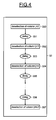
- One way of deselecting the columns non-simultaneously is, as illustrated in FIG. 4, to mutually shift their deselection over time by introducing a delay between each column deselection.
- the deselection of the column j + 2 is carried out at the step 330. Then, the column j + 3 deselected at the step 332 with a delay 331 with respect to the deselection of the column j + 2.
- the column j + k-2 is deselected (step 337) with a delay 336 relative to the deselection of the column j + k-3.
- FIGS. 5 and 6 schematically illustrate an embodiment of a control device according to the invention for carrying out the method according to the invention.
- the line control circuit here comprises individual BCL1-BCLi line control blocks, of conventional structure and known per se, respectively connected to the lines of the matrix of the screen.
- the column control circuit comprises individual control blocks BCC1-BCCj respectively connected to the columns C1-Cj of the screen.
- the column control circuit also comprises, upstream of its individual control blocks, a shift register RAD, clocked by a clock signal CLK and receiving the binary data referenced DATA, and intended in particular to possibly deselect columns which have previously selected when selecting a previous row.
- the outputs of the shift register RAD are connected to the inputs of a lock memory MV whose respective outputs are connected to the inputs of the individual control blocks BCC1-BCCj.
- the lock memory MV is controlled by an activation signal STB and will output on its outputs MV1-MVj, the data present at the input of the lock memory MV.
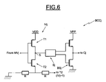
- Each individual control block BCCj comprises a control inverter IVj whose output S is connected to an intermediate block Bj generally composed of an inverter and a voltage booster.
- the structure of such a block Bj is conventional and known per se.
- the output of the block Bj is connected to a power stage BSj formed here of two NMOS transistors.
- the gates of the NMOS transistors are respectively connected to two outputs of the block Bj.
- the source of one of the NMOS transistors is connected to the voltage VPP (of the order of 70 volts) while the source of the other NMOS transistor is connected to ground.
- the other two electrodes of the NMOS transistors are connected together to the corresponding column.
- control inverter IVj comprises for example an NMOS transistor referenced T2 and a PMOS transistor referenced T1.
- the transistor T1 is connected between the supply voltage VDD, for example 3 or 5 volts, and the output S while the gates of these two transistors T1 and T2 are connected to the corresponding output MVj of the lock memory MV.
- a logic high level for example 5 volts, is applied to the gates of the two transistors T1 and T2, which has the effect of turning on the power transistor of the stage BSj power, connected to ground, and to block the other power transistor.
- the capacity of the cell is discharged and the column voltage drops by the value VPP of the value 0.
- the deselection control signals that is to say the data present at the outputs of the lock memory MV, are simultaneously delivered to the inverters IVj.
- a first solution for mutually delaying the column deselecting signals, that is to say the appearance of the falling edges FD, consists in making inverters IVj whose P-type MOS transistors have width / length ratios (W / L) different from each other. Indeed, the W / L ratio of the P-type transistor determines in particular the current that can pass through this transistor, and thereby makes it possible to adjust the instant of appearance of the falling edge of the column voltage.
- auxiliary resistive network comprising auxiliary resistors R connected in series.
- the auxiliary resistive network is connected between the second terminal (here the source) of the transistor T2 of the inverter IV of a first control block and the ground.
- the terminals of the different resistors are respectively connected to the sources of the transistors T2 of the different inverters IVj.
- This preferred embodiment is particularly advantageous since it makes it possible to produce variable delays as a function of the number of deselected columns.
- the delay introduced by an inverter IVj depends on the voltage drop in the auxiliary resistors R and these voltage drops depend on the number of outputs that switch, that is to say the number of deselected columns.
- the greater the number of outputs that switch the greater the changeover time of the inverters.
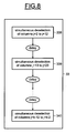
- the non-simultaneous deselection of the columns to be deselected can be carried out column by column or by groups of columns as illustrated in FIG. 8 and in FIG. 9.
- step 33 of non-simultaneous deselection of the columns the columns j + 2 to j + 12 are deselected simultaneously (step 338) and that the columns j + 13 to j + 23 are deselected simultaneously (step 339) but with a delay compared with the simultaneous deselection of the columns j + 2 to j + 12.
- the deselection of the columns j + k-12 to j + k-2 (step 340) is carried out simultaneously but with a delay with respect to the simultaneous deselection of the preceding group of columns.
- FIG. 9 illustrates another embodiment of a control device according to the invention enabling non-simultaneous deselection by groups of columns.
- FIG. 9 shows the auxiliary resistive network formed here of the auxiliary resistors R2, R3, Rn.
- the individual control blocks form several groups, here the groups G1, G2, Gn. Each group is formed in this example of two individual control blocks, illustrated in Figure 9 by the two control inverters. All the first terminals of the inverters are connected to the supply voltage VDD.
- All the second terminals of the inverters are connected to ground via the auxiliary resistive network.
- the groups are mutually separated by an auxiliary resistor of the auxiliary resistive network.
- the first group G1 formed of inverters IVI and IV2 is arranged in such a way that the second terminals of the inverters IV 1 and IV2 are connected together to a first terminal of the resistor R2.
- the second group of inverters G2 formed of the inverters IV3 and IV4 is arranged such that the second terminals of these two inverters are connected together, as well as to the second terminal of the resistor and the first terminal of the resistor R3. which separates this second group G2 from the third group G3.
- the resistance Rn separates the group Gn-1 from the group Gn formed of the inverters IVn-1 and IVn whose respective second terminals are connected together directly to the ground.
- the invention has made it possible, by acting on the mutual offset of the falling edges of the tensions of the columns to deselect, to maintain an acceptable duration for these fronts, compatible with a permissible level of electromagnetic emission.
- delay values of the order of 20 to 60 nanoseconds between the initiation of the different falling edges makes it possible to maintain an acceptable duration for these fronts.
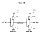
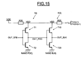
- each control block for example the control block BCC1, as illustrated in FIG.
- the shift register RAD the lock memory MV and the part of the control block BCC1, which is located upstream of the power stage BS1, in particular comprises two NAND logic gates, respectively referenced NAND POC1 and NAND BLK1.
- the first NAND logic gate POC1 has a first input adapted to receive a logic signal POC so as to be set to a high logic state and a second input connected to the corresponding output OUT _STB1 of the lock memory MV.
- the second NAND logic gate BLK1 has a first input adapted to receive another logic signal BLK so as to be set to a high logic state, and a second input connected to the output OUT_POC of the NAND logic gate POC1.
- the output OUT_BLK of the NAND gate BLK1 is connected to the power stage BS1 whose output OUT1 is connected to the column C1.
- the NAND logic gate POCj with its first input set high (POC signal high), is functionally equivalent to the inverter IV j of FIGS. 5 and 6, although that the door NAND POCj comprises in fact two inverters.
- NAND gate BLKj comprises two inverters
- this logic gate with its first input set to the high logic state (signal BLK in the high state) is functionally equivalent to another inverter, called here second inverter, IV2j, formed complementary transistors T10 and T20.
- FIGS. 12 et seq To describe embodiments and implementations making it possible to select and unselect columns non-simultaneously.
- a low logic level for example 0 volts
- a low logic level for example 0 volts
- the deselection control signals, and the selection control signals that is to say the data present at the outputs of the lock memory MV, are simultaneously delivered to the inverters IVj.
- One way of mutually shifting the onset of the falling edges of the column voltages and the rising edges of the column voltages is to use the embodiment illustrated in Figs. 13 and 14.
- FIG. 13 shows the auxiliary resistive network formed by the resistors R20 and making it possible to mutually offset the falling edges of the column voltages that must be deselected.
- auxiliary resistive network R20 In addition to this auxiliary resistive network R20, there are provided secondary means of delay comprising secondary resistors R10 connected in series.
- the secondary resistive network is connected between the first terminal of the first inverter of a first control block BCCn (FIG. 14) and the supply voltage VDD. Moreover, the terminals of the different secondary resistors R10 are respectively connected to the first terminals of the inverters IVj of at least some of the individual control blocks BCCj.
- the secondary resistive network formed by the resistors R10 thus allows non-simultaneous selection of previously deselected columns.
- FIG. 13 and / or FIG. 14 makes it possible both to select some previously unselected columns, non-simultaneously, and to deselect certain other previously selected columns, and that of also non-simultaneous way.
- auxiliary means of delay and the secondary means of delay are formed by the same means.
- each control inverter IVj and IV2j has a first terminal connected to the supply voltage VDD and a second terminal connected to ground.
- the common means then comprise a common resistive network comprising common resistors R30 connected in series.
- the common resistive network is connected between the first terminal of each inverter of a first control block BCCn and the supply voltage.
- the terminals of the various common resistors R30 are also respectively connected to the first terminals of the two inverters of at least some of the individual control blocks.
- the delay on the rising edges is generated in the NAND logic gates POC while the delay on the falling edges is generated in the NAND logic gates BLK.
- the common delay means are arranged at the level of the lock memories MV.
- each latch memory is connected to the input of an individual control block, and more particularly to the input of the NAND logic gate POC which does not receive the POC signal.
- amplification means or “buffers”
- BUFFER STB referenced BUFFER STB, all of which are capable of receiving the same input control signal STB and respectively supplying amplified control signals for respectively controlling the memories. locks.
- Each BUFFER STB amplification means has a first terminal connected to a supply voltage.
- the common resistive network here comprises common resistors R40 connected in series.
- the common resistive network is connected between the first terminal of an amplification means of a first latch memory and the supply voltage, for example the latch memory MV.
- terminals of the various common resistors R40 are respectively connected to the first terminals of the BUFFER STB amplification means of at least some of the latches.
- the delays on the falling and rising edges are generated in the signal amplification means STB.
- the common delay means are also arranged at the level of the lock memories MV.
- each latch memory is connected to the input of an individual control block, and more particularly to the input of the NAND logic gate POC which does not receive the POC signal.
- the amplification means (or “buffers") referenced BUFFER STB form here a chain. More precisely, the first amplification means BUFFER STB1 of the string is able to receive the input control signal STB and to output a amplified control signal which serves as an input control signal for the second BUFFER STB2 amplification means of the chain. And the input control signal of an amplification means current from the second is the output signal delivered by the preceding amplification means. As in the previous embodiment of FIG. 17A, the amplified control signals control the latches respectively.
- Each BUFFER STB amplification means has a first terminal connected to a supply voltage.
- the common delay means are here formed by the chain of BUFFER STBi amplification means, and the delays on the falling and rising edges are generated in the signal amplification means STB.
- FIGS. 18 and 19 make it possible to select and deselect the columns by group of columns, each group having in its figures two columns as an example, and each group being selected or deselected at a different time of the instant of deselection or selection of another group.
- the group G1 comprises the columns 1 and 2 while the group Gn comprises the columns n-1 and n.
- the power supply terminals of the two pairs of NAND POC and NAND BLK logic gates of each group are connected together and connected to the two pairs of an adjacent group by a common resistor R30 of the common resistive network.
- FIG. 19 A similar arrangement is found in FIG. 19, but this time at the level of the arrangement of the column control circuit MV. More precisely, the supply terminals of the two BUFFER STB amplification means of a group are connected together and are connected to the two amplification means of an adjacent group by a common resistor R40 of the common resistive network.
Landscapes
- Engineering & Computer Science (AREA)
- Physics & Mathematics (AREA)
- Power Engineering (AREA)
- Plasma & Fusion (AREA)
- Computer Hardware Design (AREA)
- General Physics & Mathematics (AREA)
- Theoretical Computer Science (AREA)
- Control Of Indicators Other Than Cathode Ray Tubes (AREA)
- Dram (AREA)
- Control Of Gas Discharge Display Tubes (AREA)
- Physical Or Chemical Processes And Apparatus (AREA)
Applications Claiming Priority (2)
| Application Number | Priority Date | Filing Date | Title |
|---|---|---|---|
| FR0413846A FR2880174A1 (fr) | 2004-12-23 | 2004-12-23 | Procede et dispositif de commande d'un ecran a plasma matriciel |
| FR0508735A FR2880175A1 (fr) | 2004-12-23 | 2005-08-25 | Procede et dispositif de commande d'un ecran a plasma matriciel |
Publications (2)
| Publication Number | Publication Date |
|---|---|
| EP1677281A2 true EP1677281A2 (de) | 2006-07-05 |
| EP1677281A3 EP1677281A3 (de) | 2006-09-20 |
Family
ID=36177801
Family Applications (1)
| Application Number | Title | Priority Date | Filing Date |
|---|---|---|---|
| EP05292638A Withdrawn EP1677281A3 (de) | 2004-12-23 | 2005-12-12 | Verfahren und Vorrichtung zur Steurung eines Matrix-Plasmabildschirms |
Country Status (4)
| Country | Link |
|---|---|
| US (1) | US20060139244A1 (de) |
| EP (1) | EP1677281A3 (de) |
| JP (1) | JP2006178464A (de) |
| FR (1) | FR2880175A1 (de) |
Citations (1)
| Publication number | Priority date | Publication date | Assignee | Title |
|---|---|---|---|---|
| WO2002015163A1 (fr) | 2000-08-11 | 2002-02-21 | Stmicroelectronics S.A. | Procede et circuit de commande d'un ecran a plasma |
Family Cites Families (7)
| Publication number | Priority date | Publication date | Assignee | Title |
|---|---|---|---|---|
| US6040827A (en) * | 1996-07-11 | 2000-03-21 | Hitachi, Ltd. | Driver circuit, driver integrated circuit, and display device and electronic device using the driver circuit and driver integrated circuit |
| JP3585749B2 (ja) * | 1998-11-20 | 2004-11-04 | シャープ株式会社 | 半導体装置のシステム構成及びこの半導体装置のシステム構成を用いた液晶表示装置モジュール |
| JP3426520B2 (ja) * | 1998-12-08 | 2003-07-14 | 富士通株式会社 | 表示パネルの駆動方法及び表示装置 |
| JP3708754B2 (ja) * | 1999-06-01 | 2005-10-19 | パイオニア株式会社 | プラズマディスプレイパネルの駆動装置 |
| JP2001272948A (ja) * | 2000-03-23 | 2001-10-05 | Nec Corp | プラズマディスプレイパネルの駆動方法およびプラズマディスプレイ装置 |
| JP4695770B2 (ja) * | 2001-03-28 | 2011-06-08 | パナソニック株式会社 | プラズマディスプレイ装置 |
| WO2004074913A2 (en) * | 2003-02-19 | 2004-09-02 | Bioarray Solutions Ltd. | A dynamically configurable electrode formed of pixels |
-
2005
- 2005-08-25 FR FR0508735A patent/FR2880175A1/fr not_active Withdrawn
- 2005-12-12 EP EP05292638A patent/EP1677281A3/de not_active Withdrawn
- 2005-12-21 JP JP2005367410A patent/JP2006178464A/ja active Pending
- 2005-12-22 US US11/315,789 patent/US20060139244A1/en not_active Abandoned
Patent Citations (1)
| Publication number | Priority date | Publication date | Assignee | Title |
|---|---|---|---|---|
| WO2002015163A1 (fr) | 2000-08-11 | 2002-02-21 | Stmicroelectronics S.A. | Procede et circuit de commande d'un ecran a plasma |
Also Published As
| Publication number | Publication date |
|---|---|
| EP1677281A3 (de) | 2006-09-20 |
| JP2006178464A (ja) | 2006-07-06 |
| US20060139244A1 (en) | 2006-06-29 |
| FR2880175A1 (fr) | 2006-06-30 |
Similar Documents
| Publication | Publication Date | Title |
|---|---|---|
| EP1898426A2 (de) | Mit Hilfe eines Zeilendecoders löschbarer und programmierbarer Speicher mit Phasenumwandlung | |
| EP0474534B1 (de) | Schaltung mit einstellbarer Zeitkonstante und ihre Anwendung für einstellbare Verzögerungsleitung | |
| FR2705817A1 (fr) | Appareil d'alimentation électrique pour unité d'affichage à plasma et procédés associés. | |
| EP1361583A1 (de) | Speicherzellenprogrammierungsverfahren mit Durchbruch von Antischmelzsicherungen | |
| FR2763735A1 (fr) | Etage de sortie de puissance pour la commande de cellules d'ecran a plasma | |
| TWI255461B (en) | Semiconductor memory apparatus and activation signal generation method for sense amplifier | |
| EP1630814A1 (de) | Verfahren zum Lesen von elektrisch programmier- und löschbaren Speicherzellen mit vorausgenommenem Vorladen der Bitleitungen | |
| FR2714211A1 (fr) | Dispositif du type à émission de champ. | |
| FR2880175A1 (fr) | Procede et dispositif de commande d'un ecran a plasma matriciel | |
| FR2880174A1 (fr) | Procede et dispositif de commande d'un ecran a plasma matriciel | |
| EP0678875B1 (de) | Verfahren und Schaltungen zur Löschung eines Speichers | |
| EP1755222B1 (de) | Logikzelle mit zwei isolierten redundanten Ausgängen, und integrierte Schaltung dafür | |
| EP1862999A2 (de) | Ansteuerung einer Plasmaanzeigetafel | |
| EP1486987A1 (de) | Flash-Speicher mit Mitteln zum Steuern und Auffrischen von Speicherzellen im gelöschten Zustand | |
| EP1307874B1 (de) | Verfahren und steuerschaltung für eine plasmaanzeigetafel | |
| EP0513325A1 (de) | Pulsbreitenmodulationsgenerator mit zeitvernier | |
| EP0951711A1 (de) | Verfahren zur adressierungsansteurung einer wechselstromplasmaanzeigetafel | |
| EP1131810B1 (de) | Adressierverfahren und plasmaanzeige basierend auf separaten gerade und ungerade numerierten linienadressen | |
| WO2002041292A1 (fr) | Circuit de commande d'un ecran a plasma | |
| EP0793212B1 (de) | Steuerverfahren für eine Bildanzeigetafel mit Halbtönen und Anzeigeeinrichtung zur Durchführung dieses Verfahrens | |
| EP0954865A1 (de) | Verfahren zum programmieren eines flash-eprom-speichers | |
| EP1089290B1 (de) | Speicher mit Spaltenregister und Schreibverfahren hierfür | |
| FR2860634A1 (fr) | Dispositif de commande d'un panneau d'affichage au plasma | |
| FR2903524A1 (fr) | Dispositif de memoire avec commande programmable de l'activation des amplificateurs de lecture. | |
| FR2745411A1 (fr) | Procede de commande d'un ecran de visualisation d'image utilisant le principe de la modulation de duree d'emission de lumiere, et dispositif de visualisation mettant en oeuvre le procede |
Legal Events
| Date | Code | Title | Description |
|---|---|---|---|
| PUAI | Public reference made under article 153(3) epc to a published international application that has entered the european phase |
Free format text: ORIGINAL CODE: 0009012 |
|
| AK | Designated contracting states |
Kind code of ref document: A2 Designated state(s): AT BE BG CH CY CZ DE DK EE ES FI FR GB GR HU IE IS IT LI LT LU LV MC NL PL PT RO SE SI SK TR |
|
| AX | Request for extension of the european patent |
Extension state: AL BA HR MK YU |
|
| RIN1 | Information on inventor provided before grant (corrected) |
Inventor name: TROUSSEL, GILLES Inventor name: PERMEZEL, JEAN-MARIE Inventor name: BEZAL, JEAN-RAPHAEL |
|
| PUAL | Search report despatched |
Free format text: ORIGINAL CODE: 0009013 |
|
| AK | Designated contracting states |
Kind code of ref document: A3 Designated state(s): AT BE BG CH CY CZ DE DK EE ES FI FR GB GR HU IE IS IT LI LT LU LV MC NL PL PT RO SE SI SK TR |
|
| AX | Request for extension of the european patent |
Extension state: AL BA HR MK YU |
|
| RIN1 | Information on inventor provided before grant (corrected) |
Inventor name: TROUSSEL, GILLES Inventor name: PERMEZEL, JEAN-MARIE Inventor name: BEZAL, JEAN-RAPHAEL |
|
| 17P | Request for examination filed |
Effective date: 20070301 |
|
| 17Q | First examination report despatched |
Effective date: 20070329 |
|
| AKX | Designation fees paid |
Designated state(s): DE FR GB IT |
|
| STAA | Information on the status of an ep patent application or granted ep patent |
Free format text: STATUS: THE APPLICATION IS DEEMED TO BE WITHDRAWN |
|
| 18D | Application deemed to be withdrawn |
Effective date: 20070809 |