EP1671160B1 - Verfahren zur bestimmung und/oder auswertung eines differentiellen optischen signals - Google Patents
Verfahren zur bestimmung und/oder auswertung eines differentiellen optischen signals Download PDFInfo
- Publication number
- EP1671160B1 EP1671160B1 EP04790170A EP04790170A EP1671160B1 EP 1671160 B1 EP1671160 B1 EP 1671160B1 EP 04790170 A EP04790170 A EP 04790170A EP 04790170 A EP04790170 A EP 04790170A EP 1671160 B1 EP1671160 B1 EP 1671160B1
- Authority
- EP
- European Patent Office
- Prior art keywords
- clock
- light
- receiver
- signal
- light source
- Prior art date
- Legal status (The legal status is an assumption and is not a legal conclusion. Google has not performed a legal analysis and makes no representation as to the accuracy of the status listed.)
- Active
Links
- 238000000034 method Methods 0.000 title claims abstract description 28
- 230000003287 optical effect Effects 0.000 title claims description 9
- 230000001105 regulatory effect Effects 0.000 claims abstract description 12
- 238000006073 displacement reaction Methods 0.000 claims 1
- 238000005259 measurement Methods 0.000 abstract description 4
- 230000001360 synchronised effect Effects 0.000 abstract description 3
- 230000005540 biological transmission Effects 0.000 description 10
- 230000008859 change Effects 0.000 description 5
- 230000010363 phase shift Effects 0.000 description 5
- 238000010586 diagram Methods 0.000 description 4
- 230000004907 flux Effects 0.000 description 4
- 230000008901 benefit Effects 0.000 description 3
- 238000013016 damping Methods 0.000 description 3
- 238000001514 detection method Methods 0.000 description 3
- 238000011156 evaluation Methods 0.000 description 3
- 230000005855 radiation Effects 0.000 description 3
- 230000035945 sensitivity Effects 0.000 description 3
- 238000012546 transfer Methods 0.000 description 3
- 230000004888 barrier function Effects 0.000 description 1
- 238000006243 chemical reaction Methods 0.000 description 1
- 230000008878 coupling Effects 0.000 description 1
- 238000010168 coupling process Methods 0.000 description 1
- 238000005859 coupling reaction Methods 0.000 description 1
- 230000003111 delayed effect Effects 0.000 description 1
- 230000001419 dependent effect Effects 0.000 description 1
- 230000000694 effects Effects 0.000 description 1
- 230000002349 favourable effect Effects 0.000 description 1
- 230000010354 integration Effects 0.000 description 1
- 230000001795 light effect Effects 0.000 description 1
- 230000000630 rising effect Effects 0.000 description 1
- 238000005070 sampling Methods 0.000 description 1
- 230000001960 triggered effect Effects 0.000 description 1
Images


Classifications
-
- G—PHYSICS
- G01—MEASURING; TESTING
- G01V—GEOPHYSICS; GRAVITATIONAL MEASUREMENTS; DETECTING MASSES OR OBJECTS; TAGS
- G01V8/00—Prospecting or detecting by optical means
- G01V8/10—Detecting, e.g. by using light barriers
- G01V8/20—Detecting, e.g. by using light barriers using multiple transmitters or receivers
Definitions
- the invention relates to a method for determining and / or evaluating a differential optical signal according to the preamble of claim 1.
- Photodiodes have a sensitivity dependent on the absolute brightness for modulated light, the so-called “ambient light effect".
- the received signal of a reflection light barrier depends not only on the reflectance to be measured, but also on the ambient light.
- the evaluation of the received signal is no longer reliably possible in strongly fluctuating ambient light conditions.
- a measuring method in which the transfer function of the photodiode is eliminated.
- the received signal of the photodiode thus serves only to compare two signals received in real time. If the two light sources transmit an antiphase rectangular signal, the result is a received signal of zero in the regulated circuit. That the gain of the receiver can be selected arbitrarily high because the bandpass filtered received signal is only evaluated. If the one light source is too strong, then the received signal corresponds to their clock and vice versa. A subsequent circuit recognizes this and regulates the intensity of the light sources accordingly.
- I 2 I m ⁇ D 1 D 2
- I 2 I m ⁇ D 1 D 1 + D 2
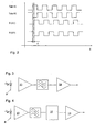
- the control method 1 is shown as a block diagram.
- Two first light sources S1, S2, here LEDs, send rectangularly modulated light in push-pull to the receiver E.
- a transmission amplitude can be regulated.
- the receiver with band-pass characteristic amplifies the received signal and supplies it to a controller 10.
- This controller in PI version, now adjusts the amplitude of the controllable first light source S1 so that the alternating signal at the receiver output is zero.
- the controller 10 evaluates the received signal synchronously with the transmitter clock, so as to detect the control direction.
- the controller 10 is divided into two parts: a detection, which transmitter is stronger, and an integrator for generating the manipulated variable.
- the integration takes place in the previously analog implementation by a classical integrator circuit, in a digital implementation, the integrator is a counter controlled by the clock, whose counting direction is controlled by the detected sign.
- the present invention is based on the object to provide a simplified digital implementation of this method as possible without loss of sensitivity.
- the compensation takes place via the light sources themselves.
- the current determined as a controlled variable in a scaled manner to the current of the correspondingly weaker light source. Switching the phase position is then equivalent to switching this additional Current from one LED to the other.
- the figures show a method for determining and / or evaluating a differential optical signal with at least two first light sources S1, S2, which transmit light in a time-sequential manner, emitting in phases.
- at least one receiver E For receiving the signal thus emitted, at least one receiver E is provided which receives the isochronous alternating light component originating from the first light sources S1, S2.
- the intensity of light irradiated in the measuring arrangement by at least one light source S1, S2, which may also be a compensation light source K, is then regulated so that the clock-synchronized alternating light component which occurs between the different phases becomes zero at the receiver E. This was explained in detail in the introduction to the description.
- the received signal is no longer evaluated and evaluated in terms of its amplitude as in an analog evaluation, but instead the received signal is determined at the receiver E with respect to the phase position and thus generates a manipulated variable.
- This manipulated variable R can be transmitted either as a light signal by a corresponding current to at least one of the first light sources S1, S2, but it is also possible to supply the whole by a current signal to the receiver by adding current.
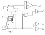
- the further light source which regulates the light intensity, can be one of the first light sources S1, S2. Alternatively, it may also be a further light source K, which is assigned to the receiver, which is controlled by this further light source K so that it changes phase by this further light source K via at least one ExOR gate 21 or at least one ExNor Gate is controlled.
- the integer value of the phase position ie, for example, +1 or -1 corresponding to 0 ° or 180 ° is integrated by means of a counter Z.
- the Digitized received signal is used as a direction signal for the receiver E.
- the received signal is fed to a flip-flop 11, wherein the clock of the flip-flop is derived from the transmission clock that, as a control signal for the counting direction of the counter Z, the signal of one of the first light sources S1 in phase and the signal of the other of the first light sources S2 is reproduced inverted (Fig. 5).
- the digitized received signal can also be used as a clock signal for the counter Z, while the counting direction is predetermined by the clock of a clock 12 which determines the clock of the first light source S1, S2 (FIG. 6).
- the received signal has compared to the clock of the clock 12 in the latter case, a phase shift of preferably 90 °.
- the received signal is buffered as a counter clock in the time domain of the edge of the clock.
- the counter reading of the counter Z may be required or may be predetermined by software.
- the manipulated variable R can additionally have a predefined or predefinable, fixed component. This is the case, in particular, when in a specific application case only a specific control range is always used. For the then remaining control range, which is determined by the variable portion of the manipulated variable, this results in a significantly increased resolution.
- This variable proportion of the manipulated variable is added to the fixed portion by current addition z. B. at the light source S1, S2, K added.
- the manipulated variable R can be added by adding current to the weaker light source or sources S1, S2, K.
- the receiver signal corresponds to the clock of transmitter S1 or transmitter S2.
- phase shift d which is caused by the transfer function of the LED driver, the receiver and to a small extent of the light transit time.
- the waveforms are shown. From top to bottom, the transmission signals of the transmitter S1 and the transmitter S2 and then the associated received signals E (S1) and E (S2) are shown, in which either transmitter S1 or S2 predominates depending on the phase.
- this rectangular signal can be obtained from the high-pass-filtered received signal by means of a comparator 14, or by a first limiting gain by means of a transimpedance amplifier 13 and an amplitude limiter 15, which is converted to the required digital level in a subsequent stage.
- This second implementation has the advantage that the saturation effects in amplifiers or the different switching times for the rising and falling edges are avoided in comparators.
- this alternating light component can be positive and negative, ie have a phase of 0 ° or 180 °, since a light emitting diode at a phase of 0 ° and the other radiates at a phase of 180 °.
- 0 ° is identified with a positive sign and 180 ° with a negative sign.
- another light source K is switched on, which is independent from the light emitting light sources works, this light can radiate out of phase and amplitude in amplitude and sign. In other words, therefore, the additional light source K can take over the compensation substantially or even alone by additional light irradiation.
- the clock-synchronous received signal is influenced in its amplitude, even in the case of complex measuring arrangements with position, direction and distance detection, such that the received signal becomes zero.
- ExOR gate 21 with two inputs can be considered as a controllable inverter. If logic zero is present at one input (control input), the output of the gate follows the second input (data input). If, on the other hand, a logic 1 is present at the control input, then the output of the gate corresponds to the inverse data input. At each output of the counter Z, such a gate is now connected and all control inputs are connected to the inverted most significant bit (MSB) of the counter. Thus, at the gate outputs compared to the count of the shown in Fig. 7 functional relationship. Also, the MSB acts as a control signal on an ExOR gate 23, through which the clock is passed to the modulator 24 of the light source K as a compensation LED. In the embodiment of FIG. 7, the transmitters S1 and S2 are not regulated.
- the counter Z can overflow.
- the control loop can not regulate due to unfavorable optical damping ratios, the control loop will oscillate, so that the counter Z will count permanently and the intensity of one or both LEDs will change cyclically.
- the overflow is prevented by a suitable wiring.
- a lock of the counter Z for each counting direction upon reaching the maximum or minimum count, a lock of the counter Z for each counting direction.
- the implementation of this interlock for example, via a coupling of the transmission output to the ENABLE input of the counter Z. The exact execution depends on the selected counter realization.
- the count changes by one step per cycle for the listed implementations.
- a suitable logic which recognizes that the last counting steps went in the same direction, also a larger counting step can be triggered. This corresponds to a D component in the controller.
- the counter Z can also have a possibility to set it to a predetermined counter reading.
- the manipulated variable is formed from two parts, namely a fixed setting in the form of an offset and a variable component, which is controlled by the controller.
- a compensation as proposed in the above-mentioned, older German Patent Application 103 00 223.5, it is therefore advisable to save the actual compensation LED and add the regulated portion additively by adding current to the respective in-phase transmitter.
Applications Claiming Priority (2)
| Application Number | Priority Date | Filing Date | Title |
|---|---|---|---|
| DE10346741A DE10346741B3 (de) | 2003-10-08 | 2003-10-08 | Verfahren zur Bestimmung und/oder Auswertung eines differentiellen optischen Signals |
| PCT/EP2004/011197 WO2005036209A1 (de) | 2003-10-08 | 2004-10-07 | Verfahren zur bestimmung und/oder auswertung eines differentiellen optischen signal |
Publications (2)
| Publication Number | Publication Date |
|---|---|
| EP1671160A1 EP1671160A1 (de) | 2006-06-21 |
| EP1671160B1 true EP1671160B1 (de) | 2007-05-02 |
Family
ID=34202432
Family Applications (1)
| Application Number | Title | Priority Date | Filing Date |
|---|---|---|---|
| EP04790170A Active EP1671160B1 (de) | 2003-10-08 | 2004-10-07 | Verfahren zur bestimmung und/oder auswertung eines differentiellen optischen signals |
Country Status (7)
| Country | Link |
|---|---|
| US (1) | US7589303B2 (es) |
| EP (1) | EP1671160B1 (es) |
| JP (1) | JP4745969B2 (es) |
| AT (1) | ATE361477T1 (es) |
| DE (2) | DE10346741B3 (es) |
| ES (1) | ES2287780T3 (es) |
| WO (1) | WO2005036209A1 (es) |
Cited By (21)
| Publication number | Priority date | Publication date | Assignee | Title |
|---|---|---|---|---|
| DE202011000870U1 (de) | 2010-07-16 | 2011-09-14 | Mechaless Systems Gmbh | Optisches Bedienelement, insbesondere Taster oder Schalter |
| EP2405283A1 (de) | 2010-07-06 | 2012-01-11 | Mechaless Systems GmbH | Optoelektronische Messanordnung mit einer Kompensationslichtquelle |
| WO2012013757A1 (de) | 2010-07-30 | 2012-02-02 | Mechaless Systems Gmbh | Opto-elektronische messanordnung mit elektro-optischer grundkopplung |
| WO2012163725A1 (de) | 2011-05-31 | 2012-12-06 | Mechaless Systems Gmbh | Display mit integriertem optischen sender |
| WO2013113456A1 (de) | 2012-02-03 | 2013-08-08 | Mechaless Systems Gmbh | Kompensation eines optischen sensors über die leiterplatte |
| DE102015002283A1 (de) | 2014-05-09 | 2015-11-12 | Elmos Semiconductor Aktiengesellschaft | Vorrichtung und Verfahren zum insbesondere dreidimensionalen optischen Scannen und Vermessen von Objekten und zur Objekterkennung mittels Lichtlaufzeitmessung und objektabhängiger Ortsauflösung mehrerer verschiedener Einzelscanner |
| DE102014019172A1 (de) | 2014-12-17 | 2016-06-23 | Elmos Semiconductor Aktiengesellschaft | Vorrichtung und Verfahren zur Unterscheidung von festen Objekten, Kochdunst und Rauch mit einem kompensierenden optischen Messsystem |
| DE102014019773A1 (de) | 2014-12-17 | 2016-06-23 | Elmos Semiconductor Aktiengesellschaft | Vorrichtung und Verfahren zur Unterscheidung von festen Objekten, Kochdunst und Rauch mittels des Displays eines Mobiltelefons |
| DE102015006174B3 (de) * | 2015-05-08 | 2016-08-11 | Elmos Semiconductor Aktiengesellschaft | Vorrichtung und Verfahren zur Vermessung einer optischen, kapazitiven, induktiven Übertragungsstrecke |
| DE102015015248A1 (de) | 2015-11-18 | 2017-05-18 | Elmos Semiconductor Aktiengesellschaft | Einfache Gestenerkennungsvorrichtung |
| DE102015015389A1 (de) | 2015-11-18 | 2017-05-18 | Elmos Semiconductor Ag | Einfache Gestenerkennungsvorrichtung |
| DE102015015246A1 (de) | 2015-11-18 | 2017-05-18 | Elmos Semiconductor Aktiengesellschaft | Einfache Gestenerkennungsvorrichtung |
| DE102015015244A1 (de) | 2015-11-18 | 2017-05-18 | Elmos Semiconductor Aktiengesellschaft | Einfache Gestenerkennungsvorrichtung |
| DE102015015245A1 (de) | 2015-11-18 | 2017-05-18 | Elmos Semiconductor Aktiengesellschaft | Einfache Gestenerkennungsvorrichtung |
| DE102015015390A1 (de) | 2015-11-18 | 2017-05-18 | Elmos Semiconductor Ag | Einfache Gestenerkennungsvorrichtung |
| DE102017106811A1 (de) | 2016-05-09 | 2017-11-09 | Elmos Semiconductor Aktiengesellschaft | Vorrichtung und zugehöriges Verfahren zur selbständigen Adresskonfiguration konfektionierbarer, flexibler LED-Bänder |
| DE102017106813A1 (de) | 2016-05-09 | 2017-11-09 | Elmos Semiconductor Aktiengesellschaft | Vorrichtung und zugehöriges Verfahren zur selbständigen Adresskonfiguration konfektionierbarer, flexibler Sensor-Bänder |
| DE102017106812A1 (de) | 2016-05-09 | 2017-11-09 | Elmos Semiconductor Aktiengesellschaft | Vorrichtung und zugehöriges Verfahren zur selbständigen Adresskonfiguration konfektionierbarer, flexibler LED-Sensor-Bänder |
| DE102017100308B3 (de) | 2016-12-06 | 2018-05-30 | Elmos Semiconductor Aktiengesellschaft | Vorrichtung und Verfahren zur Vermessung einer optischen, kapazitiven, induktiven Übertragungsstrecke mit verringerter EMV Empfindlichkeit |
| DE102017100306A1 (de) | 2017-01-09 | 2018-07-12 | Elmos Semiconductor Aktiengesellschaft | Vorrichtung und Verfahren zur Vermessung einer optischen, kapazitiven, induktiven Übertragungsstrecke mittels Mehrfachmodulation |
| DE102017100305A1 (de) | 2017-01-09 | 2018-07-12 | Elmos Semiconductor Aktiengesellschaft | Vorrichtung und Verfahren zur Vermessung einer optischen, kapazitiven, induktiven Übertragungsstrecke mittels Mehrfachmodulation |
Families Citing this family (19)
| Publication number | Priority date | Publication date | Assignee | Title |
|---|---|---|---|---|
| DE102005050451A1 (de) * | 2005-10-19 | 2007-05-03 | Imos Gubela Gmbh | Rauchdetektor |
| WO2008122938A2 (en) * | 2007-04-06 | 2008-10-16 | Koninklijke Philips Electronics N.V. | Line-of-sight optical detection system, and communication system |
| DE102007040957A1 (de) * | 2007-08-30 | 2009-03-05 | Miele & Cie. Kg | Upright-Staubsauger |
| EP2602635B1 (de) | 2011-12-06 | 2014-02-19 | ELMOS Semiconductor AG | Verfahren zur Vermessung einer Übertragungsstrecke mittels kompensierender Amplitudenmessung und Delta-Sigma-Methode sowie Vorrichtung zur Durchführung des Verfahrens |
| EP2631674A1 (de) * | 2012-02-23 | 2013-08-28 | ELMOS Semiconductor AG | Verfahren und Sensorsystem zur Vermessung der Eigenschaften einer Übertragungsstrecke eines Messsystems zwischen Sender und Empfänger |
| EP2653885A1 (de) | 2012-04-18 | 2013-10-23 | ELMOS Semiconductor AG | Sensorsystem und Verfahren zur Vermessung der Übertragungseigenschaften einer Übertragungsstrecke eines Messsystems zwischen einem Sender und einem Empfänger |
| DE102013002676B4 (de) | 2013-02-12 | 2023-06-29 | Elmos Semiconductor Se | Kompensiertes Sensorsystem mit einem in der Sensitivität regelbaren Empfänger als kompensierendes Element |
| WO2014131385A1 (de) | 2013-02-27 | 2014-09-04 | Elmos Semiconductor Ag | Multifunktionales optisches mikro-sensor-system |
| DE102014002486B4 (de) | 2013-02-27 | 2017-10-19 | Elmos Semiconductor Aktiengesellschaft | Kompensierendes optisches Sensorsystem |
| EP3036561B1 (de) | 2013-08-22 | 2018-01-31 | Elmos Semiconductor Aktiengesellschaft | Störkompensierte vorrichtung zur vermessung einer optischen signalübertragungsstrecke |
| DE102014002194B4 (de) | 2014-02-12 | 2017-10-19 | Elmos Semiconductor Aktiengesellschaft | Kompensierendes optisches Mikrosystem |
| EP2924466B1 (de) | 2014-03-25 | 2020-06-03 | Elmos Semiconductor Aktiengesellschaft | Sensorsystem zur Erkennung mindestens eines Objekts in einer Übertragungsstrecke |
| EP2924459A1 (de) | 2014-03-25 | 2015-09-30 | ELMOS Semiconductor AG | Sensorsystem zur Erkennung mindestens eines Objekts in einer Übertragungsstrecke |
| EP2924460A1 (de) | 2014-03-25 | 2015-09-30 | ELMOS Semiconductor AG | Sensorsystem zur Erkennung mindestens eines Objekts in einer Übertragungsstrecke mittels einer Diode |
| US9937124B2 (en) | 2014-09-11 | 2018-04-10 | International Business Machines Corporation | Microchip substance delivery devices having low-power electromechanical release mechanisms |
| DE102014017237A1 (de) | 2014-11-21 | 2016-05-25 | Mechaless Systems Gmbh | Messsystem zur energiesparenden optischen Abstandsmessung |
| US9734371B2 (en) * | 2015-03-31 | 2017-08-15 | International Business Machines Corporation | Hybrid tag for radio frequency identification system |
| US10881788B2 (en) | 2015-10-30 | 2021-01-05 | International Business Machines Corporation | Delivery device including reactive material for programmable discrete delivery of a substance |
| PL3208582T3 (pl) * | 2016-02-17 | 2021-05-31 | Mettler-Toledo Gmbh | Różnicowy układ pomiarowy i waga z kompensacją siły |
Family Cites Families (9)
| Publication number | Priority date | Publication date | Assignee | Title |
|---|---|---|---|---|
| JPS62291508A (ja) * | 1986-06-12 | 1987-12-18 | Stanley Electric Co Ltd | 物体検出装置 |
| US5254853A (en) * | 1990-02-14 | 1993-10-19 | Stefan Reich | Optical sensing device |
| DE4004530C2 (de) * | 1990-02-14 | 1999-07-29 | Stefan Reich | Optische Abstandsmessung |
| ES2110763T3 (es) * | 1993-07-02 | 1998-02-16 | Gerd Reime | Dispositivo para la medicion o deteccion de una modificacion en un elemento reflectante. |
| US5610394A (en) * | 1996-04-29 | 1997-03-11 | Itron, Inc. | Rotation monitor disturbance neutralization system |
| JP2000208012A (ja) * | 1999-01-11 | 2000-07-28 | Yamatake Corp | 物体検出センサ |
| DE10106998C2 (de) * | 2000-11-04 | 2003-01-23 | Stefan Reich | Verfahren und Vorrichtung zur optischen Objekterfassung |
| DE10318764A1 (de) * | 2002-05-08 | 2003-11-20 | Stefan Reich | Verfahren und Vorrichtung zur optischen Objekterfassung |
| DE10300223B3 (de) * | 2003-01-03 | 2004-06-24 | Gerd Reime | Optoelektronische Messanordnung mit Fremdlichtkompensation sowie Verfahren zur phasenkorrekten Kompensation eines Signals der Messanordnung |
-
2003
- 2003-10-08 DE DE10346741A patent/DE10346741B3/de not_active Expired - Fee Related
-
2004
- 2004-10-07 EP EP04790170A patent/EP1671160B1/de active Active
- 2004-10-07 JP JP2006530112A patent/JP4745969B2/ja active Active
- 2004-10-07 WO PCT/EP2004/011197 patent/WO2005036209A1/de active IP Right Grant
- 2004-10-07 AT AT04790170T patent/ATE361477T1/de not_active IP Right Cessation
- 2004-10-07 US US10/575,148 patent/US7589303B2/en active Active
- 2004-10-07 DE DE502004003717T patent/DE502004003717D1/de active Active
- 2004-10-07 ES ES04790170T patent/ES2287780T3/es active Active
Non-Patent Citations (1)
| Title |
|---|
| None * |
Cited By (38)
| Publication number | Priority date | Publication date | Assignee | Title |
|---|---|---|---|---|
| US9012827B2 (en) | 2010-07-06 | 2015-04-21 | Mechaless Systems Gmbh | Optoelectronic measuring system with a compensation light source |
| EP2405283A1 (de) | 2010-07-06 | 2012-01-11 | Mechaless Systems GmbH | Optoelektronische Messanordnung mit einer Kompensationslichtquelle |
| WO2012004048A1 (de) | 2010-07-06 | 2012-01-12 | Mechaless Systems Gmbh | Optoelektronische messanordnung mit einer kompensationslichtquelle |
| DE102010027499A1 (de) | 2010-07-16 | 2012-01-19 | Mechaless Systems Gmbh | Optisches Bedienelement, insbesondere Taster oder Schalter |
| DE202011000870U1 (de) | 2010-07-16 | 2011-09-14 | Mechaless Systems Gmbh | Optisches Bedienelement, insbesondere Taster oder Schalter |
| WO2012007236A1 (de) | 2010-07-16 | 2012-01-19 | Mechaless Systems Gmbh | Optisches bedienelement, insbesondere taster oder schalter |
| US8748804B2 (en) | 2010-07-16 | 2014-06-10 | Mechaless Systems Gmbh | Optical pushbutton or switch |
| US8766154B2 (en) | 2010-07-30 | 2014-07-01 | Mechaless Systems Gmbh | Opto-electronic measuring arrangement with electro-optical basic coupling |
| WO2012013757A1 (de) | 2010-07-30 | 2012-02-02 | Mechaless Systems Gmbh | Opto-elektronische messanordnung mit elektro-optischer grundkopplung |
| EP2418512A1 (de) | 2010-07-30 | 2012-02-15 | Mechaless Systems GmbH | Optoelektronische Messanordnung mit Fremdlichtkompensation |
| KR101355293B1 (ko) | 2010-07-30 | 2014-01-23 | 메카레스 시스템스 게엠베하 | 전기 광학 기본 커플링을 가진 광전자 측정 장치 |
| WO2012163725A1 (de) | 2011-05-31 | 2012-12-06 | Mechaless Systems Gmbh | Display mit integriertem optischen sender |
| WO2013113456A1 (de) | 2012-02-03 | 2013-08-08 | Mechaless Systems Gmbh | Kompensation eines optischen sensors über die leiterplatte |
| US9641244B2 (en) | 2012-02-03 | 2017-05-02 | Mechaless Systems Gmbh | Compensation for an optical sensor via a printed circuit board |
| DE102015002283A1 (de) | 2014-05-09 | 2015-11-12 | Elmos Semiconductor Aktiengesellschaft | Vorrichtung und Verfahren zum insbesondere dreidimensionalen optischen Scannen und Vermessen von Objekten und zur Objekterkennung mittels Lichtlaufzeitmessung und objektabhängiger Ortsauflösung mehrerer verschiedener Einzelscanner |
| DE102015002282A1 (de) | 2014-05-09 | 2015-11-12 | Elmos Semiconductor Aktiengesellschaft | Vorrichtung und Verfahren zum insbesondere dreidimensionalen optischen Scannen und Vermessen von Objekten und zur Objekterkennung mittels Lichtlaufzeitmessung |
| DE102015002271A1 (de) | 2014-05-09 | 2015-11-26 | Elmos Semiconductor Aktiengesellschaft | Vorrichtung und Verfahren zum insbesondere dreidimensionalen optischen Scannen und Vermessen von Objekten und zur Objekterkennung mittels Lichtlaufzeitmessung |
| DE102015002270A1 (de) | 2014-05-09 | 2015-11-26 | Elmos Semiconductor Aktiengesellschaft | Vorrichtung und Verfahren zum insbesondere dreidimensionalen optischen Scannen, Vermessen und Klassifizieren von Objekten und zur Objekterkennung mittels Lichtlaufzeitmessung |
| DE102015002283B4 (de) | 2014-05-09 | 2023-01-19 | Elmos Semiconductor Se | Vorrichtung zum insbesondere dreidimensionalen optischen Scannen und Vermessen von Objekten und zur Objekterkennung mittels Lichtlaufzeitmessung und objektabhängiger Ortsauflösung mehrerer verschiedener Einzelscanner |
| DE102014019773A1 (de) | 2014-12-17 | 2016-06-23 | Elmos Semiconductor Aktiengesellschaft | Vorrichtung und Verfahren zur Unterscheidung von festen Objekten, Kochdunst und Rauch mittels des Displays eines Mobiltelefons |
| DE102014019172A1 (de) | 2014-12-17 | 2016-06-23 | Elmos Semiconductor Aktiengesellschaft | Vorrichtung und Verfahren zur Unterscheidung von festen Objekten, Kochdunst und Rauch mit einem kompensierenden optischen Messsystem |
| DE102014019773B4 (de) | 2014-12-17 | 2023-12-07 | Elmos Semiconductor Se | Vorrichtung und Verfahren zur Unterscheidung von festen Objekten, Kochdunst und Rauch mittels des Displays eines Mobiltelefons |
| DE102014019172B4 (de) | 2014-12-17 | 2023-12-07 | Elmos Semiconductor Se | Vorrichtung und Verfahren zur Unterscheidung von festen Objekten, Kochdunst und Rauch mit einem kompensierenden optischen Messsystem |
| DE102015006174B3 (de) * | 2015-05-08 | 2016-08-11 | Elmos Semiconductor Aktiengesellschaft | Vorrichtung und Verfahren zur Vermessung einer optischen, kapazitiven, induktiven Übertragungsstrecke |
| DE102015015248A1 (de) | 2015-11-18 | 2017-05-18 | Elmos Semiconductor Aktiengesellschaft | Einfache Gestenerkennungsvorrichtung |
| DE102015015389A1 (de) | 2015-11-18 | 2017-05-18 | Elmos Semiconductor Ag | Einfache Gestenerkennungsvorrichtung |
| DE102015015246A1 (de) | 2015-11-18 | 2017-05-18 | Elmos Semiconductor Aktiengesellschaft | Einfache Gestenerkennungsvorrichtung |
| DE102015015244A1 (de) | 2015-11-18 | 2017-05-18 | Elmos Semiconductor Aktiengesellschaft | Einfache Gestenerkennungsvorrichtung |
| DE102015015245A1 (de) | 2015-11-18 | 2017-05-18 | Elmos Semiconductor Aktiengesellschaft | Einfache Gestenerkennungsvorrichtung |
| DE102015015390A1 (de) | 2015-11-18 | 2017-05-18 | Elmos Semiconductor Ag | Einfache Gestenerkennungsvorrichtung |
| DE102017106813A1 (de) | 2016-05-09 | 2017-11-09 | Elmos Semiconductor Aktiengesellschaft | Vorrichtung und zugehöriges Verfahren zur selbständigen Adresskonfiguration konfektionierbarer, flexibler Sensor-Bänder |
| DE102017106812A1 (de) | 2016-05-09 | 2017-11-09 | Elmos Semiconductor Aktiengesellschaft | Vorrichtung und zugehöriges Verfahren zur selbständigen Adresskonfiguration konfektionierbarer, flexibler LED-Sensor-Bänder |
| DE102017106811A1 (de) | 2016-05-09 | 2017-11-09 | Elmos Semiconductor Aktiengesellschaft | Vorrichtung und zugehöriges Verfahren zur selbständigen Adresskonfiguration konfektionierbarer, flexibler LED-Bänder |
| DE102017100308B3 (de) | 2016-12-06 | 2018-05-30 | Elmos Semiconductor Aktiengesellschaft | Vorrichtung und Verfahren zur Vermessung einer optischen, kapazitiven, induktiven Übertragungsstrecke mit verringerter EMV Empfindlichkeit |
| DE102017100306A1 (de) | 2017-01-09 | 2018-07-12 | Elmos Semiconductor Aktiengesellschaft | Vorrichtung und Verfahren zur Vermessung einer optischen, kapazitiven, induktiven Übertragungsstrecke mittels Mehrfachmodulation |
| DE102017100305A1 (de) | 2017-01-09 | 2018-07-12 | Elmos Semiconductor Aktiengesellschaft | Vorrichtung und Verfahren zur Vermessung einer optischen, kapazitiven, induktiven Übertragungsstrecke mittels Mehrfachmodulation |
| DE102017100305B4 (de) | 2017-01-09 | 2021-08-12 | Elmos Semiconductor Se | Vorrichtung und Verfahren zur Vermessung einer optischen, kapazitiven, induktiven Übertragungsstrecke mittels Mehrfachmodulation |
| DE102017100306B4 (de) | 2017-01-09 | 2021-08-12 | Elmos Semiconductor Se | Vorrichtung und Verfahren zur Vermessung einer optischen, kapazitiven, induktiven Übertragungsstrecke mittels Mehrfachmodulation |
Also Published As
| Publication number | Publication date |
|---|---|
| WO2005036209A1 (de) | 2005-04-21 |
| US7589303B2 (en) | 2009-09-15 |
| ES2287780T3 (es) | 2007-12-16 |
| JP2007508528A (ja) | 2007-04-05 |
| US20080042043A1 (en) | 2008-02-21 |
| DE10346741B3 (de) | 2005-03-24 |
| ATE361477T1 (de) | 2007-05-15 |
| EP1671160A1 (de) | 2006-06-21 |
| JP4745969B2 (ja) | 2011-08-10 |
| DE502004003717D1 (de) | 2007-06-14 |
Similar Documents
| Publication | Publication Date | Title |
|---|---|---|
| EP1671160B1 (de) | Verfahren zur bestimmung und/oder auswertung eines differentiellen optischen signals | |
| DE102007005187B4 (de) | Verfahren und Vorrichtung zur Bestimmung einer Entfernung zu einem rückstrahlenden Objekt | |
| DE102005045993B4 (de) | Verfahren zur Lichtlaufzeitmessung | |
| EP2850387B1 (de) | Optisches entfernungsmessgerät mit kalibriereinrichtung zum berücksichtigen von übersprechen | |
| EP2817657B1 (de) | Verfahren und sensorsystem zur vermessung der eigenschaften einer übertragungsstrecke eines messsystems zwischen sender und empfänger | |
| EP2405283A1 (de) | Optoelektronische Messanordnung mit einer Kompensationslichtquelle | |
| EP1529194B1 (de) | Verfahren und vorrichtung zur optischen distanzmessung | |
| WO2008009387A1 (de) | Optisches distanzmessverfahren und entsprechender optischer distanzmesser | |
| WO2017148772A1 (de) | Vorrichtung zur wandlung einer zeitlichen verzögerung eines zwischen einem sender und einem empfänger übertragenen signals | |
| EP2159600A1 (de) | Elektro-optischer Detektor zur Erkennung des Vorhandenseins und/oder der Annäherung eines Objekts | |
| DE19757716A1 (de) | Optische Verschiebungsmeßeinrichtung und optisches Verschiebungsmeßsystem | |
| DE202010005371U1 (de) | Optoelektronische Entfernungsmessvorrichtung | |
| DE102015006174B3 (de) | Vorrichtung und Verfahren zur Vermessung einer optischen, kapazitiven, induktiven Übertragungsstrecke | |
| EP1585234A1 (de) | Photomischdetektor (PMD)-System und Verfahren zum Betreiben desselben | |
| EP1952178B1 (de) | Entfernungsmessgerät und verfahren zum bestimmen einer entfernung | |
| DE10350489B4 (de) | Optischer Sensor | |
| DE102020119396B4 (de) | Störarme optische Messvorrichtung | |
| DE102008004025B4 (de) | Optischer Sensor | |
| DE19849585C2 (de) | Vorrichtung und Verfahren zur Bestimmung der Fluoreszenz einer Probe | |
| DE102017100305A1 (de) | Vorrichtung und Verfahren zur Vermessung einer optischen, kapazitiven, induktiven Übertragungsstrecke mittels Mehrfachmodulation | |
| DE10331376B3 (de) | Optischer Sensor | |
| DE102004059604B4 (de) | Optoelektronische Vorrichtung | |
| EP2944984B1 (de) | Verfahren zum bearbeiten eines start-signalzugs und mess- oder prüfvorrichtung | |
| DE102019002013A1 (de) | Doppel-Lock-In-Verstärker | |
| DE10035135A1 (de) | Verfahren und Vorrichtung zur Entfernungsmessung |
Legal Events
| Date | Code | Title | Description |
|---|---|---|---|
| PUAI | Public reference made under article 153(3) epc to a published international application that has entered the european phase |
Free format text: ORIGINAL CODE: 0009012 |
|
| 17P | Request for examination filed |
Effective date: 20060422 |
|
| AK | Designated contracting states |
Kind code of ref document: A1 Designated state(s): AT BE BG CH CY CZ DE DK EE ES FI FR GB GR HU IE IT LI LU MC NL PL PT RO SE SI SK TR |
|
| GRAP | Despatch of communication of intention to grant a patent |
Free format text: ORIGINAL CODE: EPIDOSNIGR1 |
|
| DAX | Request for extension of the european patent (deleted) | ||
| GRAS | Grant fee paid |
Free format text: ORIGINAL CODE: EPIDOSNIGR3 |
|
| GRAA | (expected) grant |
Free format text: ORIGINAL CODE: 0009210 |
|
| AK | Designated contracting states |
Kind code of ref document: B1 Designated state(s): AT BE BG CH CY CZ DE DK EE ES FI FR GB GR HU IE IT LI LU MC NL PL PT RO SE SI SK TR |
|
| PG25 | Lapsed in a contracting state [announced via postgrant information from national office to epo] |
Ref country code: FI Free format text: LAPSE BECAUSE OF FAILURE TO SUBMIT A TRANSLATION OF THE DESCRIPTION OR TO PAY THE FEE WITHIN THE PRESCRIBED TIME-LIMIT Effective date: 20070502 |
|
| REG | Reference to a national code |
Ref country code: GB Ref legal event code: FG4D Free format text: NOT ENGLISH |
|
| REG | Reference to a national code |
Ref country code: CH Ref legal event code: EP |
|
| REG | Reference to a national code |
Ref country code: IE Ref legal event code: FG4D Free format text: LANGUAGE OF EP DOCUMENT: GERMAN |
|
| REF | Corresponds to: |
Ref document number: 502004003717 Country of ref document: DE Date of ref document: 20070614 Kind code of ref document: P |
|
| PG25 | Lapsed in a contracting state [announced via postgrant information from national office to epo] |
Ref country code: SE Free format text: LAPSE BECAUSE OF FAILURE TO SUBMIT A TRANSLATION OF THE DESCRIPTION OR TO PAY THE FEE WITHIN THE PRESCRIBED TIME-LIMIT Effective date: 20070802 |
|
| GBT | Gb: translation of ep patent filed (gb section 77(6)(a)/1977) |
Effective date: 20070801 |
|
| ET | Fr: translation filed | ||
| NLV1 | Nl: lapsed or annulled due to failure to fulfill the requirements of art. 29p and 29m of the patents act | ||
| PG25 | Lapsed in a contracting state [announced via postgrant information from national office to epo] |
Ref country code: PL Free format text: LAPSE BECAUSE OF FAILURE TO SUBMIT A TRANSLATION OF THE DESCRIPTION OR TO PAY THE FEE WITHIN THE PRESCRIBED TIME-LIMIT Effective date: 20070502 |
|
| REG | Reference to a national code |
Ref country code: ES Ref legal event code: FG2A Ref document number: 2287780 Country of ref document: ES Kind code of ref document: T3 |
|
| REG | Reference to a national code |
Ref country code: IE Ref legal event code: FD4D |
|
| PG25 | Lapsed in a contracting state [announced via postgrant information from national office to epo] |
Ref country code: PT Free format text: LAPSE BECAUSE OF FAILURE TO SUBMIT A TRANSLATION OF THE DESCRIPTION OR TO PAY THE FEE WITHIN THE PRESCRIBED TIME-LIMIT Effective date: 20071002 Ref country code: NL Free format text: LAPSE BECAUSE OF FAILURE TO SUBMIT A TRANSLATION OF THE DESCRIPTION OR TO PAY THE FEE WITHIN THE PRESCRIBED TIME-LIMIT Effective date: 20070502 Ref country code: SI Free format text: LAPSE BECAUSE OF FAILURE TO SUBMIT A TRANSLATION OF THE DESCRIPTION OR TO PAY THE FEE WITHIN THE PRESCRIBED TIME-LIMIT Effective date: 20070502 Ref country code: BG Free format text: LAPSE BECAUSE OF FAILURE TO SUBMIT A TRANSLATION OF THE DESCRIPTION OR TO PAY THE FEE WITHIN THE PRESCRIBED TIME-LIMIT Effective date: 20070802 Ref country code: IE Free format text: LAPSE BECAUSE OF FAILURE TO SUBMIT A TRANSLATION OF THE DESCRIPTION OR TO PAY THE FEE WITHIN THE PRESCRIBED TIME-LIMIT Effective date: 20070502 Ref country code: DK Free format text: LAPSE BECAUSE OF FAILURE TO SUBMIT A TRANSLATION OF THE DESCRIPTION OR TO PAY THE FEE WITHIN THE PRESCRIBED TIME-LIMIT Effective date: 20070502 |
|
| PG25 | Lapsed in a contracting state [announced via postgrant information from national office to epo] |
Ref country code: SK Free format text: LAPSE BECAUSE OF FAILURE TO SUBMIT A TRANSLATION OF THE DESCRIPTION OR TO PAY THE FEE WITHIN THE PRESCRIBED TIME-LIMIT Effective date: 20070502 |
|
| PLBE | No opposition filed within time limit |
Free format text: ORIGINAL CODE: 0009261 |
|
| STAA | Information on the status of an ep patent application or granted ep patent |
Free format text: STATUS: NO OPPOSITION FILED WITHIN TIME LIMIT |
|
| 26N | No opposition filed |
Effective date: 20080205 |
|
| BERE | Be: lapsed |
Owner name: MECHALESS SYSTEMS G.M.B.H. Effective date: 20071031 |
|
| PG25 | Lapsed in a contracting state [announced via postgrant information from national office to epo] |
Ref country code: GR Free format text: LAPSE BECAUSE OF FAILURE TO SUBMIT A TRANSLATION OF THE DESCRIPTION OR TO PAY THE FEE WITHIN THE PRESCRIBED TIME-LIMIT Effective date: 20070803 |
|
| PG25 | Lapsed in a contracting state [announced via postgrant information from national office to epo] |
Ref country code: RO Free format text: LAPSE BECAUSE OF FAILURE TO SUBMIT A TRANSLATION OF THE DESCRIPTION OR TO PAY THE FEE WITHIN THE PRESCRIBED TIME-LIMIT Effective date: 20070502 Ref country code: MC Free format text: LAPSE BECAUSE OF NON-PAYMENT OF DUE FEES Effective date: 20071031 |
|
| PG25 | Lapsed in a contracting state [announced via postgrant information from national office to epo] |
Ref country code: BE Free format text: LAPSE BECAUSE OF NON-PAYMENT OF DUE FEES Effective date: 20071031 |
|
| PG25 | Lapsed in a contracting state [announced via postgrant information from national office to epo] |
Ref country code: EE Free format text: LAPSE BECAUSE OF FAILURE TO SUBMIT A TRANSLATION OF THE DESCRIPTION OR TO PAY THE FEE WITHIN THE PRESCRIBED TIME-LIMIT Effective date: 20070502 |
|
| PG25 | Lapsed in a contracting state [announced via postgrant information from national office to epo] |
Ref country code: AT Free format text: LAPSE BECAUSE OF NON-PAYMENT OF DUE FEES Effective date: 20071007 |
|
| REG | Reference to a national code |
Ref country code: CH Ref legal event code: PL |
|
| PG25 | Lapsed in a contracting state [announced via postgrant information from national office to epo] |
Ref country code: CY Free format text: LAPSE BECAUSE OF FAILURE TO SUBMIT A TRANSLATION OF THE DESCRIPTION OR TO PAY THE FEE WITHIN THE PRESCRIBED TIME-LIMIT Effective date: 20070502 |
|
| PG25 | Lapsed in a contracting state [announced via postgrant information from national office to epo] |
Ref country code: LU Free format text: LAPSE BECAUSE OF NON-PAYMENT OF DUE FEES Effective date: 20071007 |
|
| PG25 | Lapsed in a contracting state [announced via postgrant information from national office to epo] |
Ref country code: TR Free format text: LAPSE BECAUSE OF FAILURE TO SUBMIT A TRANSLATION OF THE DESCRIPTION OR TO PAY THE FEE WITHIN THE PRESCRIBED TIME-LIMIT Effective date: 20070502 Ref country code: HU Free format text: LAPSE BECAUSE OF FAILURE TO SUBMIT A TRANSLATION OF THE DESCRIPTION OR TO PAY THE FEE WITHIN THE PRESCRIBED TIME-LIMIT Effective date: 20071103 |
|
| PG25 | Lapsed in a contracting state [announced via postgrant information from national office to epo] |
Ref country code: CH Free format text: LAPSE BECAUSE OF NON-PAYMENT OF DUE FEES Effective date: 20081031 Ref country code: LI Free format text: LAPSE BECAUSE OF NON-PAYMENT OF DUE FEES Effective date: 20081031 |
|
| PGFP | Annual fee paid to national office [announced via postgrant information from national office to epo] |
Ref country code: CZ Payment date: 20090930 Year of fee payment: 6 |
|
| PG25 | Lapsed in a contracting state [announced via postgrant information from national office to epo] |
Ref country code: CZ Free format text: LAPSE BECAUSE OF NON-PAYMENT OF DUE FEES Effective date: 20101007 |
|
| REG | Reference to a national code |
Ref country code: DE Ref legal event code: R082 Ref document number: 502004003717 Country of ref document: DE Representative=s name: PATENTANWAELTE REINHARDT & POHLMANN PARTNERSCH, DE Ref country code: DE Ref legal event code: R082 Ref document number: 502004003717 Country of ref document: DE Representative=s name: DURM & PARTNER PATENTANWAELTE, DE |
|
| REG | Reference to a national code |
Ref country code: GB Ref legal event code: 732E Free format text: REGISTERED BETWEEN 20111201 AND 20111207 |
|
| REG | Reference to a national code |
Ref country code: DE Ref legal event code: R082 Ref document number: 502004003717 Country of ref document: DE Representative=s name: DURM & PARTNER PATENTANWAELTE, DE |
|
| REG | Reference to a national code |
Ref country code: ES Ref legal event code: PC2A Owner name: ELMOS SEMICONDUCTOR AG Effective date: 20120305 |
|
| REG | Reference to a national code |
Ref country code: FR Ref legal event code: TP Owner name: ELMOS SEMICONDUCTOR AG, DE Effective date: 20120210 |
|
| REG | Reference to a national code |
Ref country code: DE Ref legal event code: R082 Ref document number: 502004003717 Country of ref document: DE Representative=s name: DURM & PARTNER PATENTANWAELTE, DE Effective date: 20110805 Ref country code: DE Ref legal event code: R081 Ref document number: 502004003717 Country of ref document: DE Owner name: ELMOS SEMICONDUCTOR AG, DE Free format text: FORMER OWNER: MECHALESS SYSTEMS GMBH, 76131 KARLSRUHE, DE Effective date: 20120214 Ref country code: DE Ref legal event code: R082 Ref document number: 502004003717 Country of ref document: DE Representative=s name: DURM & PARTNER PATENTANWAELTE, DE Effective date: 20120214 Ref country code: DE Ref legal event code: R081 Ref document number: 502004003717 Country of ref document: DE Owner name: ELMOS SEMICONDUCTOR AKTIENGESELLSCHAFT, DE Free format text: FORMER OWNER: MECHALESS SYSTEMS GMBH, 76131 KARLSRUHE, DE Effective date: 20120214 |
|
| PGFP | Annual fee paid to national office [announced via postgrant information from national office to epo] |
Ref country code: IT Payment date: 20121024 Year of fee payment: 9 Ref country code: ES Payment date: 20121023 Year of fee payment: 9 Ref country code: GB Payment date: 20121023 Year of fee payment: 9 |
|
| GBPC | Gb: european patent ceased through non-payment of renewal fee |
Effective date: 20131007 |
|
| PG25 | Lapsed in a contracting state [announced via postgrant information from national office to epo] |
Ref country code: GB Free format text: LAPSE BECAUSE OF NON-PAYMENT OF DUE FEES Effective date: 20131007 |
|
| PG25 | Lapsed in a contracting state [announced via postgrant information from national office to epo] |
Ref country code: IT Free format text: LAPSE BECAUSE OF NON-PAYMENT OF DUE FEES Effective date: 20131007 |
|
| REG | Reference to a national code |
Ref country code: DE Ref legal event code: R082 Ref document number: 502004003717 Country of ref document: DE Representative=s name: DURM & PARTNER PATENTANWAELTE, DE |
|
| REG | Reference to a national code |
Ref country code: DE Ref legal event code: R081 Ref document number: 502004003717 Country of ref document: DE Owner name: ELMOS SEMICONDUCTOR AKTIENGESELLSCHAFT, DE Free format text: FORMER OWNER: ELMOS SEMICONDUCTOR AG, 44227 DORTMUND, DE Effective date: 20150108 Ref country code: DE Ref legal event code: R082 Ref document number: 502004003717 Country of ref document: DE Representative=s name: DURM & PARTNER PATENTANWAELTE, DE Effective date: 20150108 |
|
| REG | Reference to a national code |
Ref country code: ES Ref legal event code: FD2A Effective date: 20150407 |
|
| PG25 | Lapsed in a contracting state [announced via postgrant information from national office to epo] |
Ref country code: ES Free format text: LAPSE BECAUSE OF NON-PAYMENT OF DUE FEES Effective date: 20131008 |
|
| REG | Reference to a national code |
Ref country code: FR Ref legal event code: PLFP Year of fee payment: 12 |
|
| REG | Reference to a national code |
Ref country code: FR Ref legal event code: PLFP Year of fee payment: 13 |
|
| REG | Reference to a national code |
Ref country code: FR Ref legal event code: PLFP Year of fee payment: 14 |
|
| REG | Reference to a national code |
Ref country code: FR Ref legal event code: PLFP Year of fee payment: 15 |
|
| REG | Reference to a national code |
Ref country code: DE Ref legal event code: R082 Ref document number: 502004003717 Country of ref document: DE Representative=s name: DURM PATENTANWAELTE PARTG MBB, DE Ref country code: DE Ref legal event code: R081 Ref document number: 502004003717 Country of ref document: DE Owner name: ELMOS SEMICONDUCTOR SE, DE Free format text: FORMER OWNER: ELMOS SEMICONDUCTOR AKTIENGESELLSCHAFT, 44227 DORTMUND, DE |
|
| P01 | Opt-out of the competence of the unified patent court (upc) registered |
Effective date: 20230530 |
|
| PGFP | Annual fee paid to national office [announced via postgrant information from national office to epo] |
Ref country code: FR Payment date: 20231023 Year of fee payment: 20 Ref country code: DE Payment date: 20231018 Year of fee payment: 20 |