EP1670610B1 - Traitement au laser pour depot thermosensible a l'echelle mesoscopique - Google Patents
Traitement au laser pour depot thermosensible a l'echelle mesoscopique Download PDFInfo
- Publication number
- EP1670610B1 EP1670610B1 EP04789155.1A EP04789155A EP1670610B1 EP 1670610 B1 EP1670610 B1 EP 1670610B1 EP 04789155 A EP04789155 A EP 04789155A EP 1670610 B1 EP1670610 B1 EP 1670610B1
- Authority
- EP
- European Patent Office
- Prior art keywords
- laser
- target
- deposit
- aerosol
- deposition
- Prior art date
- Legal status (The legal status is an assumption and is not a legal conclusion. Google has not performed a legal analysis and makes no representation as to the accuracy of the status listed.)
- Not-in-force
Links
Images


Classifications
-
- C—CHEMISTRY; METALLURGY
- C08—ORGANIC MACROMOLECULAR COMPOUNDS; THEIR PREPARATION OR CHEMICAL WORKING-UP; COMPOSITIONS BASED THEREON
- C08F—MACROMOLECULAR COMPOUNDS OBTAINED BY REACTIONS ONLY INVOLVING CARBON-TO-CARBON UNSATURATED BONDS
- C08F2/00—Processes of polymerisation
- C08F2/46—Polymerisation initiated by wave energy or particle radiation
-
- B—PERFORMING OPERATIONS; TRANSPORTING
- B05—SPRAYING OR ATOMISING IN GENERAL; APPLYING FLUENT MATERIALS TO SURFACES, IN GENERAL
- B05D—PROCESSES FOR APPLYING FLUENT MATERIALS TO SURFACES, IN GENERAL
- B05D1/00—Processes for applying liquids or other fluent materials
- B05D1/02—Processes for applying liquids or other fluent materials performed by spraying
-
- B—PERFORMING OPERATIONS; TRANSPORTING
- B05—SPRAYING OR ATOMISING IN GENERAL; APPLYING FLUENT MATERIALS TO SURFACES, IN GENERAL
- B05D—PROCESSES FOR APPLYING FLUENT MATERIALS TO SURFACES, IN GENERAL
- B05D3/00—Pretreatment of surfaces to which liquids or other fluent materials are to be applied; After-treatment of applied coatings, e.g. intermediate treating of an applied coating preparatory to subsequent applications of liquids or other fluent materials
- B05D3/06—Pretreatment of surfaces to which liquids or other fluent materials are to be applied; After-treatment of applied coatings, e.g. intermediate treating of an applied coating preparatory to subsequent applications of liquids or other fluent materials by exposure to radiation
-
- B—PERFORMING OPERATIONS; TRANSPORTING
- B82—NANOTECHNOLOGY
- B82Y—SPECIFIC USES OR APPLICATIONS OF NANOSTRUCTURES; MEASUREMENT OR ANALYSIS OF NANOSTRUCTURES; MANUFACTURE OR TREATMENT OF NANOSTRUCTURES
- B82Y10/00—Nanotechnology for information processing, storage or transmission, e.g. quantum computing or single electron logic
-
- C—CHEMISTRY; METALLURGY
- C23—COATING METALLIC MATERIAL; COATING MATERIAL WITH METALLIC MATERIAL; CHEMICAL SURFACE TREATMENT; DIFFUSION TREATMENT OF METALLIC MATERIAL; COATING BY VACUUM EVAPORATION, BY SPUTTERING, BY ION IMPLANTATION OR BY CHEMICAL VAPOUR DEPOSITION, IN GENERAL; INHIBITING CORROSION OF METALLIC MATERIAL OR INCRUSTATION IN GENERAL
- C23C—COATING METALLIC MATERIAL; COATING MATERIAL WITH METALLIC MATERIAL; SURFACE TREATMENT OF METALLIC MATERIAL BY DIFFUSION INTO THE SURFACE, BY CHEMICAL CONVERSION OR SUBSTITUTION; COATING BY VACUUM EVAPORATION, BY SPUTTERING, BY ION IMPLANTATION OR BY CHEMICAL VAPOUR DEPOSITION, IN GENERAL
- C23C18/00—Chemical coating by decomposition of either liquid compounds or solutions of the coating forming compounds, without leaving reaction products of surface material in the coating; Contact plating
- C23C18/02—Chemical coating by decomposition of either liquid compounds or solutions of the coating forming compounds, without leaving reaction products of surface material in the coating; Contact plating by thermal decomposition
-
- C—CHEMISTRY; METALLURGY
- C23—COATING METALLIC MATERIAL; COATING MATERIAL WITH METALLIC MATERIAL; CHEMICAL SURFACE TREATMENT; DIFFUSION TREATMENT OF METALLIC MATERIAL; COATING BY VACUUM EVAPORATION, BY SPUTTERING, BY ION IMPLANTATION OR BY CHEMICAL VAPOUR DEPOSITION, IN GENERAL; INHIBITING CORROSION OF METALLIC MATERIAL OR INCRUSTATION IN GENERAL
- C23C—COATING METALLIC MATERIAL; COATING MATERIAL WITH METALLIC MATERIAL; SURFACE TREATMENT OF METALLIC MATERIAL BY DIFFUSION INTO THE SURFACE, BY CHEMICAL CONVERSION OR SUBSTITUTION; COATING BY VACUUM EVAPORATION, BY SPUTTERING, BY ION IMPLANTATION OR BY CHEMICAL VAPOUR DEPOSITION, IN GENERAL
- C23C18/00—Chemical coating by decomposition of either liquid compounds or solutions of the coating forming compounds, without leaving reaction products of surface material in the coating; Contact plating
- C23C18/14—Decomposition by irradiation, e.g. photolysis, particle radiation or by mixed irradiation sources
- C23C18/143—Radiation by light, e.g. photolysis or pyrolysis
-
- G—PHYSICS
- G21—NUCLEAR PHYSICS; NUCLEAR ENGINEERING
- G21K—TECHNIQUES FOR HANDLING PARTICLES OR IONISING RADIATION NOT OTHERWISE PROVIDED FOR; IRRADIATION DEVICES; GAMMA RAY OR X-RAY MICROSCOPES
- G21K1/00—Arrangements for handling particles or ionising radiation, e.g. focusing or moderating
- G21K1/006—Manipulation of neutral particles by using radiation pressure, e.g. optical levitation
-
- H—ELECTRICITY
- H01—ELECTRIC ELEMENTS
- H01L—SEMICONDUCTOR DEVICES NOT COVERED BY CLASS H10
- H01L2924/00—Indexing scheme for arrangements or methods for connecting or disconnecting semiconductor or solid-state bodies as covered by H01L24/00
- H01L2924/01—Chemical elements
- H01L2924/01022—Titanium [Ti]
-
- H—ELECTRICITY
- H01—ELECTRIC ELEMENTS
- H01L—SEMICONDUCTOR DEVICES NOT COVERED BY CLASS H10
- H01L2924/00—Indexing scheme for arrangements or methods for connecting or disconnecting semiconductor or solid-state bodies as covered by H01L24/00
- H01L2924/01—Chemical elements
- H01L2924/01046—Palladium [Pd]
-
- H—ELECTRICITY
- H01—ELECTRIC ELEMENTS
- H01L—SEMICONDUCTOR DEVICES NOT COVERED BY CLASS H10
- H01L2924/00—Indexing scheme for arrangements or methods for connecting or disconnecting semiconductor or solid-state bodies as covered by H01L24/00
- H01L2924/01—Chemical elements
- H01L2924/01056—Barium [Ba]
-
- H—ELECTRICITY
- H01—ELECTRIC ELEMENTS
- H01L—SEMICONDUCTOR DEVICES NOT COVERED BY CLASS H10
- H01L2924/00—Indexing scheme for arrangements or methods for connecting or disconnecting semiconductor or solid-state bodies as covered by H01L24/00
- H01L2924/19—Details of hybrid assemblies other than the semiconductor or other solid state devices to be connected
- H01L2924/1901—Structure
- H01L2924/1904—Component type
- H01L2924/19043—Component type being a resistor
-
- H—ELECTRICITY
- H10—SEMICONDUCTOR DEVICES; ELECTRIC SOLID-STATE DEVICES NOT OTHERWISE PROVIDED FOR
- H10K—ORGANIC ELECTRIC SOLID-STATE DEVICES
- H10K71/00—Manufacture or treatment specially adapted for the organic devices covered by this subclass
- H10K71/10—Deposition of organic active material
- H10K71/16—Deposition of organic active material using physical vapour deposition [PVD], e.g. vacuum deposition or sputtering
- H10K71/162—Deposition of organic active material using physical vapour deposition [PVD], e.g. vacuum deposition or sputtering using laser ablation
Definitions
- the present invention relates generally to the field of maskless direct write deposition of materials, including but not limited to mesoscale electronic structures, using aerodynamic focusing of an aerosolized fluid or particle suspension onto heat-sensitive targets, wherein laser radiation is preferably used to process the deposit to its final state.
- Thick film and thin film processes for the deposition of electronic structures are well developed, but have limitations due to the high processing temperatures required, or due to the need for expensive masks and vacuum chambers. Thick film processes typically require processing temperatures ranging from approximately 500 to 1000 °C. Thin film techniques use processing temperatures ranging from approximately 400 to 3000 °C, depending on the type of process and the material deposited. Due to inherent high processing temperatures, thick film and thin film techniques are generally limited to deposition onto ceramic, glass, silicon, and other targets having a damage threshold temperature above approximately 400 °C.
- a thin film process used to form ceramic metallo-organic thin films is disclosed in U. S. Patent No. 5, 064, 684 .
- This process casts a liquid metallo-organic ceramic precursor solution to form a layer on a target.
- the deposit is heated to a low temperature to create an amorphous layer.
- the process then heats a selected area to a high temperature using localized heating, creating a patterned area of polycrystalline ceramic having electro-optic properties.
- Kydd uses a mixture of metal powders and metallo-organic decomposition compounds in an organic liquid vehicle to form thick films.
- the compound is applied to a target using a deposition process such as silk screening, in which bonding is complete at temperatures of less than 450 °C.
- US 2003/048314 A recites methods and apparatus for the deposition of a source material are disclosed.
- An atomizer renders a supply of source material into many discrete particles.
- a force applicator propels the particles in continuous, parallel streams of discrete particles.
- a collimator controls the direction of flight of the particles in the stream prior to their deposition on a substrate.
- the viscosity of the particles may be controlled to enable complex depositions of non-conformal or three-dimensional surfaces.
- the invention also includes a wide variety of substrate treatments which may occur before, during or after deposition.
- a virtual or cascade impactor may be employed to remove selected particles from the deposition stream.
- US 6,025,037 A recites a sol-gel coating of conductive materials, such as ITO, which is applied to a substrate, for example a display window of a cathode ray tube, is cured by means of a laser.
- a sol-gel coating of conductive materials such as ITO
- a substrate for example a display window of a cathode ray tube
- a laser is cured by means of a laser.
- This is preferably carried out in a water-containing atmosphere, for example an aqueous aerosol and/or a hydrogen-containing gas, such as a forming gas. This results in a stable resistance reduction by several hundred times.
- the M 3 DTM process in contrast with conventional methods for deposition of electronic materials, the M 3 DTM process, described in, for example, U. S. Patent Publication Nos. 2003/0048314 and 2003/0228124 , which are commonly owned with the present application, is a direct printing technique that does not require the use of vacuum chambers, masks, or extensive post-deposition processing.
- the M 3 DTM-process may be used to deposit a variety of materials with little or no material waste, and has also been used to deposit materials which do not require high temperature processing on low temperature substrates. In order to facilitate this, various low temperature ink systems have been developed.
- inks are typically either precursor-based, nanoparticle-based, or they can be combinations of the two.
- Metal-organic precursor chemistries have a specific advantage in that the precursors can decompose to pure metal at very low temperatures, 150-250 °C range. Because of this the inks can be deposited on many plastics and then heated to decompose to metal. The drawback is that the metal yield of precursor inks is typically low and is in the 1-10% range. The low yield reduces the overall deposition rates.
- Metal nanoparticles also have drastically reduced treatment temperatures. Because of their high surface energy, nanoparticles will melt at temperatures hundreds of degrees lower than micron-sized particles. Nanoparticle inks in particular have been shown to sinter in the 150-250 °C range. The metal yield of nanoparticle inks can be in the 10-50% range, which leads to highly efficient deposition.
- the M 3 DTM process has been used to deposit and laser process silver (at 150 °C) on an FR4 substrate, which has a damage threshold of less than 200 °C, with no damage to the substrate.
- Glasses may undergo crystallization and melting, and metals may undergo oxidation, recrystallization, grain growth, reversed hardening, and melting, when subjected to excessive heat. Ceramics. may also undergo thermal damage in the form of unfavorable phase changes that may lead to cracking or loss of material or electrical properties, vaporization of volatile components, and oxidation (for ceramics that are not oxides). For example, densification on low temperature substrates has only been achievable for materials that can be densified at temperatures below the damage threshold of the substrate.
- the present invention is a method for depositing a material on a target according to current claim 1.
- the electrical property preferably comprises resistivity and the target is optionally nonplanar.
- the damage threshold is preferably less than 200 °C.
- the aerosol stream preferably comprises one or more materials selected from the groups consisting of liquid molecular chemical precursors and colloidal or particle suspensions.
- the aerosol stream preferably further comprises one or more materials generated from the groups comprising a metallo-organic precursor, a metallo-organic precursor; a colloidal metal solution; a metal paste; a metal nanoparticle suspension; a ceramic precursor; a ceramic paste; a resistor precursor solution; a resistor paste; an inorganic semiconductor suspension; a polymeric precursor solution; a colloidal suspension of metal, dielectric, or resistor particles; and any combination thereof.
- the aerosol stream preferably comprises droplets or particles having a diameter of less than approximately 10 micrometres (microns).
- the generating step preferably comprises, using ultrasonic transduction or pneumatic aerosolization.
- the aerosol jet preferably comprises an annular flow, preferably an inner aerosol-laden flow surrounded by a sheath gas flow that confines the inner aerosol-laden flow.
- the annular flow preferably focuses the aerosol stream to mesoscale dimensions.
- the deposited feature size is preferably greater than or equal to approximately four micrometres (microns).
- the feature size of the deposit after laser processing is preferably at least approximately one micrometre (micron).
- the depositing step preferably comprises providing relative motion of the target and the aerosol stream.
- the method preferably further comprises the step of pre-processing the aerosol stream prior to the depositing step.
- the pre-processing step preferably comprises a process selected from the group consisting of humidifying the aerosol stream, drying the aerosol stream, cooling the aerosol stream, increasing the vapor content of a constituent of the aerosol stream, and increasing the vapor content of a second material that is not a constituent of the aerosol stream.
- the method of the present invention preferably further comprises the step of post-processing the deposit prior to the processing step.
- the post-processing step preferably comprises an action selected from the group consisting of thermal heating, reducing the ambient pressure, irradiating with electromagnetic radiation, and combinations thereof.
- the deposit optionally comprises a width that is approximately equal to a diameter of a beam from the laser or is greater than a diameter of a beam from the laser.
- the deposition step and the processing step are preferably performed simultaneously.
- the processing step preferably comprises at least one process selected from the group consisting of chemical decomposition, polymerization, sintering, and melting.
- the target preferably comprises a material selected from the group consisting of polycarbonate, polyethylene terephthalate, polymethyl methacrylate, polytetrafluoroethylene, polyester, and various epoxies.
- the laser preferably comprises a diode laser.
- the laser power is preferably approximately 10 milliwatts.
- the laser preferably comprises a continuous wave mode or a pulsed wave mode.
- the energy of the pulsed wave mode is preferably several microjoules.
- the processing step preferably comprises delivering a laser beam to the target using either or both of a system of lenses and mirrors and an optical fiber.
- the laser beam is optionally delivered to the target apart from the aerosol stream, thereby resulting in serial process deposition and laser processing.
- An advantage of the present invention is that it may be used to deposit materials including but not limited to conductors, semiconductors, insulators, and resistive and inductive structures.
- Another advantage of the present invention is that low damage threshold target materials may be deposited on, including but not limited to plastics, ceramics, epoxies, and biological tissue.
- a further advantage of the present invention is that the desired structure may be deposited onto a planar or non-planar target.
- the present invention provides a method for maskless, non-contact direct printing of mesoscale structures of various materials onto heat-sensitive targets.
- Material deposition is preferably accomplished using the M 3 DTMaerosol-jetting device, which utilizes an aerosolized stream delivered to the target via an annularly flowing aerosol jet.
- the method preferably uses low-power laser radiation to heat the aerosol-jetted material to its final state.
- Combining the M 3 DTM process with laser processing extends the utilization of the technique to temperature sensitive applications, in which the temperature required to treat the deposited material approaches or exceeds the thermal damage threshold of the target.
- the process is capable of precise, selective deposition with little or no material waste.
- a positional accuracy of approximately 1 micron is achievable with laser processing and a subsequent material removal process, such as etching or rinsing, with a tool-to-target standoff distance of as much as approximately five millimeters.
- heat-sensitive process means any process in which the temperature required to process the deposited material, i. e. drive it to its desired state, approaches or exceeds the damage threshold of the target, wherein the target is not globally heated above its damage threshold. Typically, such targets have a low damage threshold.
- a heat-sensitive process may have a wide range of temperatures.
- Laser processing of M 3 DTM-deposited structures preferably combines highly localized aerodynamic deposition of material with a highly localized energy source providing the ability to focus laser radiation to a diameter that is approximately the same as the width of the deposited line, to engineer material formulations to be highly absorbing at the laser wavelength, to deposit nanoparticle suspensions, and to deliver laser energy in short pulses or by rapidly scanning over a deposit enables processing of various materials onto heat-sensitive targets with little or no damage to the target.
- the present invention is capable of depositing materials at room temperature. Many of these materials can cure at room temperature.
- One advantage offered by the invention is the ability to lay down materials in patterns in the mesoscale range (from 1 to 1000 micrometres (microns)). If the material needs a thermal post treatment, the deposition can be followed with a laser treatment.
- the laser beam provides a highly localized thermal and photonic treatment of the material. The laser beam is capable of treating only the deposited material after deposition without affecting the underlying substrate.
- the present invention allows for a variety of substrate treatments during the deposition process.
- Alternative embodiments of the invention include capabilities for heating the substrate by laser illumination or by increasing the ambient temperature.
- the substrate may also be cooled during deposition by reducing ambient temperature.
- Other alternative treatment steps may include photoactivation with a laser, irradiation with infrared light, or illumination with an arc lamp.
- Another substrate treatment comprises a washing or rinsing process.
- Typical thick film techniques deposit materials that must be fired well above 400 °C, limiting the process to high-temperature substrates.
- the present invention is capable of depositing materials onto heat-sensitive substrates, and then using thermal or laser processing to obtain the desired properties by virtue of the initial precursor chemistry or localized laser heating.
- the present invention can deposit electronic materials onto low-cost polymer substrates that cannot withstand high-temperature oven fires.
- the present invention comprises a maskless deposition process that fills a niche in the mesoscale regime between thick and thin film.
- the invention is capable of depositing multiple materials into fine geometries on both planar and curved substrates.
- the materials can be commercial pastes or custom, low-fire inks. Laser processing allows the materials to be densified on heat-sensitive polymers.
- the present invention may be applied to a wide range of applications.
- the ability to deposit fine lines over curved and stepped surface suggests applications in writing interconnect wires between IC chips and PWB.
- the ability to deposit multiple materials lends to applications in multilayer components as well as to encapsulating components once they are built.
- the ability to fire materials on heat-sensitive substrate allows discrete components to be directly written on polymers.
- the deposition technique used in the present invention is called Maskless Mesoscale Material Deposition (M 3 DTM).
- the technique uses an annularly flowing aerosol jet to deposit features as small as approximately 4 micrometres (microns).
- the jet consists of an inner aerosol-laden flow surrounded by a sheath gas flow that confines and focuses the inner flow.
- the two flows may also consist of fluids. Focusing of the aerosol stream to one-tenth of the exit orifice diameter has been demonstrated at distances of up to approximately five millimeters from the orifice.
- the orifice diameter preferably ranges from 100- 500 micrometres (microns).
- the aerosol stream is preferably formed by aerosolizing a sample using an ultrasonic transducer and/or pneumatic nebulizer 22, as shown in Figure 1 .
- the aerosol stream is preferably comprised of a liquid molecular chemical precursor and/or colloidal or particle or nanoparticle suspension. These preferably further comprise a metallo-organic precursor; a colloidal metal solution; a metal paste; a ceramic precursor; a ceramic paste; a resistor precursor solution; a resistor paste; an inorganic semiconductor suspension; a polymeric precursor solution; a colloidal suspension of metal, dielectric, or resistor particles, or the like, or any combination thereof.
- any material suitable for laser heating can be employed as a feedstock in the practice of the present invention, depending on the intended application.
- dielectric materials such as barium titanate or silicon dioxide, resistive materials such as a ruthenates, metal dielectric composites such as silver+barium titanate, conductive materials such as silver, copper, or gold, semiconducting materials such as silicon, germanium, or gallium nitride, magnetic materials such as MnZn and FeZn, ceramics such as alumina or zirconium diboride, and cermets may all be deposited.
- the precursor solvent or suspending fluid used is preferably chosen based on its compatibility with the target material.
- the M 3 DTM apparatus preferably comprises an upper module for aerosolizing liquid chemical precursors or colloidal or particle suspensions, a deposition module for directing, focusing, and depositing the resulting aerosol, laser module 10 for delivering and focusing laser radiation, and a control module for monitoring and controlling the process parameters.
- the M 3 DTM deposition module preferably consists of virtual impactor 24, flowhead 12, and material shutter assembly 26 with mechanical shutter 28.
- the aerosol stream preferably is processed by virtual impactor 24, which reduces the volume of gas in which the aerosol is entrained.
- the aerosol-laden carrier gas preferably bypasses virtual impactor 24, and enters flowhead 12 immediately after the aerosolization process.
- the carrier gas preferably comprises either or both of a compressed air or an inert gas, and can comprise a solvent vapor.
- a flow controller preferably monitors and controls the mass throughput of the aerosolized stream.
- the aerosolized stream preferably enters flowhead 12 via aerosol inlet 20 in heater assembly 16 mounted on the apparatus, and is preferably collimated as it flows through an orifice centered on the longitudinal axis of flowhead 12.
- Heater assembly 16 is preferably used to heat the aerosolized material to remove solvent or to modify the viscosity of the sample.
- the aerosol stream emerges with droplets and/or particles and is preferably entrained and surrounded by a sheath gas.
- the sheath gas comprises either or both of a compressed air or an inert gas, and can optionally comprise solvent vapor content or a fluid.
- the sheath gas enters through sheath air inlet 18, preferably located on heater assembly 16 below the aerosol inlet 20, and then enters the lower portion of flowhead 12, preferably through multiple internal ports, forming an annular flow surrounding the aerosol stream.
- the two streams exit the chamber through a second orifice directed at the target.
- the sheath gas forms a boundary layer that prevents particles from depositing onto the orifice wall.
- This annular configuration is capable of focusing the aerosol stream to approximately one-fifth to one-tenth the size of the orifice diameter, enabling deposition of features on the target with dimensions as small as approximately 4 micrometres (microns).
- the standoff distance between the system's flowhead and the target is typically 3 to 5 mm, enabling deposition onto non-planar surfaces.
- Patterns are preferably written by translating a computer-controlled target platen, located under stationary flowhead 12, using a CAD-based Virtual Masking (VMToolTM) software application.
- VMToolTM Virtual Masking
- flowhead 12 may be translated under computer control while maintaining the target in a fixed position, or both flowhead 12 and the target may be moved simultaneously.
- Software such as VMToolTM, preferably defines a toolpath for printing the desired circuit or element.
- the deposited material is processed with at least one laser.
- deposited material may be processed at a higher temperature than the damage threshold of the target to drive the deposit to the desired state in order achieve electrical properties near that of the bulk material, preferably with little or no physical, chemical, optical changes, or other damage to the underlying target.
- the processing may comprise chemical decomposition, polymerization, sintering, melting, or the like.
- Target materials may comprise any material with a low damage threshold temperature, including but are not limited to polymers, glasses, metals, various epoxies, and ceramics, more specifically such materials as polycarbonate, polyethylene terephthalate (PET), polymethyl methacrylate (PMMA), polytetrafluoroethylene (Teflon®), and polyester.
- PET polyethylene terephthalate
- PMMA polymethyl methacrylate
- Teflon® polytetrafluoroethylene
- the target may be locally heated above its damage threshold without impact its global properties. Further, in many cases this local heating improves adhesion of the deposited material to the target.
- the present invention provides for processing a deposit at temperatures of up to approx. 50 °C or more higher than the damage threshold of the target. With the laser treatment of the present invention, sintering inks on low-melting-temperature plastics is possible.
- the size of the deposit is in the mesoscale range, and can vary from several micrometres (microns) to approximately 1 millimeter, bridging the gap between thin film and thick film processes.
- the aerosol stream may optionally be preprocessed prior to deposition, most commonly before introduction of the aerosol into the flowhead.
- the pre-processing step may comprise processes including but not limited to increasing the solvent or suspending medium vapor content, partially decomposing, humidifying, drying, heating, or cooling of the aerosol, carrier gas, and/or sheath gas.
- the target is optionally conditioned by heating before deposition, preferably via a heater, infrared lamp, or high power diode laser.
- the deposited pattern may also optionally be post-processed prior to the laser treatment.
- Post-processing optionally comprises thermally heating the deposit in an ambient or reduced pressure environment, irradiating the deposit with electromagnetic radiation, or a combination thereof.
- These optional steps processing are preferably performed to remove solvent or other residual volatile constituents of the precursor solvent or the particle suspending fluid.
- drying it is preferably performed in a manner such that the deposit retains some of its fluid properties, so that wetting and coalescence of the aerosol droplets into a continuous structure is accomplished. In this manner, the amount of laser energy required for heating and vaporization of the solvent is reduced.
- deposition and processing of the aerosol stream may optionally be performed simultaneously.
- the type of processing laser used may vary, and is dependent on the optical and thermal properties of the deposit and the target.
- the laser power may be as small as approximately 10 milliwatts, enabling the use of an inexpensive diode laser.
- the laser may comprise a continuous wave mode or a pulsed wave mode.
- the pulsed wave mode optionally comprises an energy as low as several microjoules.
- the laser beam is preferably delivered to the target using a series of mirrors and lenses that collimate and route the beam to a focusing lens.
- the beam may optionally be delivered using fiber optics, wherein the laser beam is launched into an appropriate optical fiber and delivered through the fiber to the focusing lens.
- the laser radiation is preferably to a spot size of less than one micron. Modification of the laser beam profile facilitates material processing on heat- sensitive targets.
- the laser beam is preferably expanded and collimated before being truncated and focused onto the target.
- the expansion of the beam is performed to decrease the focused spot size, and to aid in truncation.
- Truncation of the beam minimizes the inherent Gaussian variation in laser power across the beam profile.
- the truncation step allows for more uniform heating of the deposited line in the direction perpendicular to the target motion, and aids in the reduction of target damage at the boundaries of the deposit.
- the wavelength of the laser is preferably chosen so that laser radiation is absorbed by the deposit but not by the target. That is, ideally the deposit is highly absorptive and the target is highly transmissive, that is, transparent or nearly transparent, at the wavelength of the laser.
- the material may be sintered, decomposed, or otherwise processed, and most of the heat delivered to the target is the heat conducted through the deposit/target interface.
- the target material is highly absorbing at the laser wavelength, and the deposit is weakly absorbing. In this case, the deposit is heated through conduction of thermal energy from the target/deposit boundary. The former case is ideal for laser processing of heat-sensitive targets. In normal applications, absorption of the laser radiation by both the target and the deposit occurs.
- the laser may optionally be delivered to the target via the flowhead.
- the laser energy may alternatively be delivered to the target at a location that is different from the location of the flowhead, so that a serial process is used for deposition and laser processing.
- Simultaneous deposition and laser processing may also be used to form vias between target layers.
- the laser is preferably directed along the flowhead axis, emerges from the flowhead orifice, and heats the aerosol during flight and after deposition onto the target.
- the laser radiation can optionally be delivered parallel to the target surface, so that in-flight processing of the aerosol is enabled without the laser heating the target.
- the aerosol particles can be rendered partially or wholly depositable, or optionally melted, in flight by exposure to a laser of sufficient intensity for a sufficient period of time. Exposure time may be increased by slowing feedstock velocity and/or increasing the area of laser through which the feedstock passes. In some instances it may be desirable to use a plurality of laser beams having a common area of intersection.
- Sufficient energy is preferably imparted to the feedstock in-flight to render the feedstock depositable and promote adhesion to the substrate without causing significant interfacial damage of the substrate or deposited feedstock, that is, while only providing sufficient peripheral heating of the substrate to facilitate adhesion without a significant level of surface modification.
- This embodiment preferably reduces or eliminates the need to create a molten puddle on the target surface. This broadens the range of materials that can be used as deposition substrates.
- Melting the particles prior to deposition according to this embodiment reduces residual stress contained within the fabricated structures, enabling a broader range of materials to be deposited onto dissimilar materials.
- the impacting characteristics of the depositable particle will behave similarly to thermal spray processes in which shrinkage of the substrate surface is counteracted by outward force due to the particle droplet spreading on impact.
- the deposited pattern or structure preferably comprises a desired width that is approximately the same as the diameter of the laser beam so that direct irradiation of the target is limited or completely eliminated.
- the desired width of the deposit may alternatively be greater than the diameter of the laser beam.
- the present invention may be used to deposit a film of material with dimensions greater than the diameter of the laser beam.
- the laser beam is rastered, or scanned back and forth, over the desired area of the deposit to pattern a specific structure, and the unprocessed material is removed from the target.
- some shrinking of the deposit may occur, for example during the processes of chemical decomposition or sintering.
- the final dimensions of the deposit are mostly determined by the deposition mass flux, the target speed, and the fluid properties of the deposited material.
- laser treatment is used to raise the temperature of the deposit to its decomposition or curing temperature.
- a chemical decomposition or cross-linking takes place due to the input of laser energy, such that the precursor changes its molecular state.
- the change in molecular state results in the conversion of the precursor material to the desired material.
- the decomposition process also entails emission of gaseous byproducts. Laser processing of precursor deposits on various targets is possible without incurring damage to the target.
- Example 2 Laser Sintering of Particle Suspensions and Commercial Pastes and Inks
- the M 3 DTTM process is capable of selective sintering of a two-component paste consisting of low and high-melting temperature particles such as low-melting point glass and metal, dielectric, resistive, or ferromagnetic materials.
- Laser processing may be used to sinter commercial resistor and conductor pastes, and may also be used to sinter pastes for other electronic materials such as dielectrics and ferromagnetics.
- commercial pastes which typically have viscosities of 100, 000 centipoise or greater-are preferably diluted in a suitable solvent and pneumatically aerosolized for deposition.
- Laser sintering of M 3 DTTM -deposited commercial inks can also be accomplished on plastic and other heat-sensitive targets with damage thresholds of approximately 100 °C.
- the commercial inks that may be processed using the M 3 DTTM method and laser sintering typically consist of suspensions with particle diameters ranging from hundreds of nanometers to several microns.
- the inks may include, but are not limited to, conductive, resistive, and dielectrics formulations.
- Example 3 Laser Sintering of M 3 DTTM-Deposited Nanoparticle Inks
- Laser sintering of M 3 DTTM -deposited nanoparticle inks has also been used to form metal lines on heat-sensitive targets.
- the laser-sintered nanoparticle deposits preferably exhibit resistivities near that of the bulk metal.
- Laser sintering of M 3 DTM-deposited nanoparticles to near bulk resistivities can be accomplished with 100 mW or less of visible or ultraviolet laser radiation. Infrared laser radiation may also be used for laser sintering of nanoparticles, given that the absorption of the ink is tailored to the wavelength of the laser.
- the nanoparticle ink is preferably deposited in a fluid form, so that particle suspension is maintained, and the laser is then preferably scanned over the deposit to sinter individual particles.
- Simultaneous deposition and sintering of the nanoparticle ink may be performed to deposit lines with greater thickness than lines deposited using a serial deposition and decomposition process.
- Simultaneous deposition and sintering of the nanoparticle ink can also be used to form three-dimensional microstructures on heat-sensitive targets.
- the present invention has been used to fabricate thin film transistors on plastic targets, with damage thresholds of approximately 100 to 150 °C.
- the invention can be used for solution-based fabrication of organic thin film transistors (OTFT's) on flexible targets such as PET (polyethylene terephthalate), PEN, polycarbonate, polyetheretherketone (PEEK), and polyester.
- OTFT's organic thin film transistors
- flexible targets such as PET (polyethylene terephthalate), PEN, polycarbonate, polyetheretherketone (PEEK), and polyester.
- the application of the M 3 DTTM process to fabricate OTFT's can also be extended to glass targets.
- the process can deposit and process the organic semiconductor as well as the metallization required for OTFT fabrication.
- the present invention can also be used to deposit the source and drain electrodes, the gate electrode, and the gate insulator. Channel lengths as small as approximately 4 microns can be formed.
- the ratio of the channel width to channel length is preferably held to 10 or greater, to reduce the occurrence of fringe effects.
- Other configurations include an indium-tin oxide (ITO) gate and a polyimide insulation layer.
- ITO indium-tin oxide
- Metals that can be deposited for OTFT electrode fabrication with near bulk resistivities include but are not limited to palladium, gold, and alloys thereof.
- the conductor or semiconductor material is deposited using the M 3 DTTM flowhead and then processed to the desired state using laser treatment or thermal heating.
- the invention can be used to perform solution-based deposition of an organic semiconducting material, such as a pentacene precursor, which can be processed to form the semiconducting medium of the transistor.
- the M 3 DTTM process can be used to fabricate both the OTFT backplanes and the required electrical interconnects for glass and plastic displays.
- One common technique for fabrication of interconnects on plastics uses conductive polymers, which have resistivities as high as at least several thousand times that of bulk metal.
- the M 3 DTM process contrastingly is capable of depositing on plastic targets five to ten-micron wide silver interconnect lines having resistivities approximating that of the bulk metal.
- the present invention can also be used to fabricate inorganic thin film transistors on various targets using an amorphous silicon ink and laser post-deposition processing.
- the present invention can be used to repair defects in glass and plastic flat panel display (FPD) circuitry.
- FPD glass and plastic flat panel display
- electrical opens may occur on metal structures that form interconnect lines, bus lines, or any conductive pathway that routes signals to the display circuitry.
- gaps in conductive traces may be repaired by depositing a metal precursor, a metal nanoparticle ink, or the like, or a combination thereof, forming an electrical interconnect between the open circuit.
- the deposited material is then decomposed or sintered to its final state using a local or global heating process that can include, but is not limited to, irradiation of the deposit with laser radiation, irradiation with divergent or focused non-laser radiation, or heating the deposit in a furnace.
- a local or global heating process can include, but is not limited to, irradiation of the deposit with laser radiation, irradiation with divergent or focused non-laser radiation, or heating the deposit in a furnace.
- Insufficient material deposition may occur if the viscosity of the deposited material is too low, so that material flows onto the target, and does not deposit to a sufficient height at the defect site. Cracking and poor adhesion may occur if excess material is applied to the defect site, particularly at the junction of the newly deposited structure and the end of the open line.
- the M 3 DTMprocessing parameters may be adjusted to deposit the correct thickness of material to allow for material deposition and processing without cracking or poor adhesion.
- Processing of material in the form of precursor inks, nanoparticle deposits, or combinations of the two, with good adhesion to glass and plastic targets, can be accomplished with less than approximately 100 mW of laser power.
- Inexpensive diode laser systems can therefore be used to process materials for FPD repair on glass or plastic.
- the deposited material may include, but is not limited to, silver, gold, copper, and indium-tin oxide, with linewidths as small as approximately 5 micrometres (microns).
- the most common method for fabrication of flex circuits entails a multi-step photolithographic process, and includes lamination of a metal foil to the target, deposition of a resist, exposure of the resist through a mask, development, etching, and resist removal. These processes are time-consuming, and fabrication of the mask can be expensive. The process also generates waste, since only part of the original metal film is used in the circuit.
- the M 3 DTM process proposes the use of a maskless, one-step deposition process for fabrication of flex circuitry.
- the present invention is a direct, additive process, and therefore eliminates the need for lamination, photo processing, chemical etching, and the associated material waste.
- the entire metallization process preferably requires only three steps, and is outlined in Figure 3 , along with the steps for the more conventional photolithographic process.
- the application of the M 3 DTM process to the fabrication of flex circuits can also reduce the processing time and expense for the manufacture of multilayer circuits.
- the present inventors have developed a Virtual Masking tool (VMToolT'''), a CAD-based software program that enables computer-controlled patterning of an aerosolized liquid or suspension of particles.
- VMToolT''' Virtual Masking tool
- VMTool can deposit the patterned insulating layer required between three-dimensional circuit layers.
- the M 3 DTM apparatus can be used to deposit liquid molecular precursors for gold and platinum onto various targets.
- the precursor is preferably a metallo-organic system composed of a metal salt dissolved in an organic solvent.
- the approach aerosolizes the precursor and heats the droplets in flight before depositing the aerosol onto the target.
- the precursor method can be used for direct write of gold or platinum traces with linewidths as small as from approximately one micrometres (microns). to five micrometres (microns), for targets with damage thresholds greater than approximately 400 °C.
- Nanoparticle-based gold inks offer an alternate to the precursor deposition method for depositing gold onto plastic targets.
- Gold precursor inks typically have decomposition temperatures that are several hundred degrees above the damage threshold temperature of plastics such as PET, PEEK, and PEN, precluding precursor deposition of gold.
- Nanoparticle gold inks consisting of nanometer-size gold particles preferably with diameters ranging from 1 to 20 nanometers, can significantly lower the sintering temperature, and allow for laser processing of M 3 DTM-deposited gold traces on low-temperature plastics having damage threshold temperatures as low as about 100 °C.
- the use of nanoparticle-based metal inks can lower the metal sintering temperature so that the present invention can be used for direct write metallization of plastic targets.
- the M 3 DTM process may also be used to produce multi-layered structures including but not limited to inductors and capacitors.
- the M 3 DTM process may be used to deposit material onto non-planar surfaces with height variations on the order of hundreds of micrometres (microns).
- the M 3 DTM process, followed by laser treatment has been used to fabricate functional three-layer electrical components on low temperature targets.
- a three-step process has been used to fabricate a ferrite-core inductor on a Kapton or alumina target.
- Step one was to deposit parallel lines of silver ink directly onto the target.
- the lines were approximately 100 micrometres (microns) wide, micrometre (micron) thick and 1000 micrometres (microns) in length.
- the lines were laser treated to form dense, conductive silver wires. These wires comprise one portion of the conductive traces that will eventually wrap around a ferrite core.
- Silver contact pads (1000 micron square) were also added in the first layer.
- the second step was to deposit a mixture of manganese-zinc ferrite powder and low melting temperature glass over the conductive lines. The powder was densified by scanning a laser across the deposit, which melted the glass.
- the glass flowed around the ferrite particles, forming a dense matrix material after cooling.
- the ferrite deposition step was repeated several times to buildup the deposit to about 100 micrometres (microns).
- the ferrite line lengths were about 1500 mm long.
- the final step was to deposit conductive diagonal silver lines over the ferrite core, connecting to the underlying parallel silver lines, to create the coil. Since the deposition head standoff distance is several millimeters, it is relatively simple to write over a millimeter-sized curved surface.
- the resistance of a typical coil generated using this method was on the order of several ohms.
- the inductance was 7 microHenries and the Q value was 4. 2@1 MHz.
- Figure 4 shows a micrograph of an inductor fabricated using the M 3 DTM process on Kapton target 36.
- the first layer of silver lines requires a thickness (at least 10 micrometres (microns)) sufficient to prevent shorting due to electromigration of silver to the ferrite/glass layer during laser sintering of the core.
- the top layer of diagonal silver lines is typically written over a 100-500 micrometres (microns) nonconformal surface (in this case, ferrite core 34) to connect the bottom silver lines, forming inductor coil 30.
- the bottom electrode lines of layer one are fully dense traces with heights of approximately 50 micrometres (microns).
- Contact pad 32 is 1 mm square.
- Ferrite core 34 is a 5 x 15 mm rectangle with a maximum height of 400 micrometres (microns), and is preferably formed from a manganese/zinc iron oxide and glass powder.
- the inductance curve of an M 3 DTM'-fabricated inductor printed on Kapton is shown in Figure 5 , and reveals a gradual and predictable increase from 0.8 to 1.5 microHenrys in the range from 40 Hz to 110 MHz.
- the quality factor or energy stored per cycle was 50 at 50 MHz.
- the M 3 DTM process has also been used to fabricate type-S (platinum, platinum/rhodium) thermocouples on tantalum nitride (TaN) targets.
- the platinum side of the device was written on the left arm of the thermocouple.
- the targeted alloying ratio of the platinum/rhodium arm was 90% Pt and 10% Rh.
- the devices were electrically insulated from the target using an adhesive Kapton film.
- Thin films of platinum (Pt) and platinum/rhodium (Pt/Rh) liquid precursors were deposited onto an insulating layer of polyimide. Laser decomposition was used to drive the films to the metal state.
- the figure shows a smooth transition from Pt-Pt/Rh junction 38 to Pt lead 40, which was deposited first, and to Pt/Rh (arm) lead 42, which was deposited over junction 38.
- Deposition of metal layers with a thickness of more than a few hundred nanometers may also lead to unacceptable cracking of the decomposed metal film. In this example the deposit thickness is therefore held to approximately 0.2 to 0.5 micrometres (microns).
- Metallization requiring greater thickness may be obtained by using an iterative method to deposit and decompose several layers.
- the calibration curve for an M 3 DTM-fabricated thermocouple is shown in Figure 7 .
- the corresponding curve for a standard type-S thermocouple with a reference temperature of 0 °C is also shown.
- the device shows a characteristic curve that is very similar to the standard curve.
- the slope of the experimental curve is within less than 3% of the slope of the standard curve (7. 50x10-3 mV/ °C versus 7. 73x10 mV/ °C) from 65 to 177 °C.
- the difference in output may be due to the use of a reference temperature of approximately 21 °C, rather than 0 °C.
- the invention may be used for metallization of plastic targets and UV curable polymers (bus lines, electrodes, interconnects, etc.), deposition of passive electronic components onto circuit board, deposition of embedded passives on circuit board, fabrication of vias between target layers, and metallization of epoxies.
- the M 3 DTM process has been used to deposit and sinter silver on polycarbonate target material. Because of the high processing temperatures needed for decomposition of the silver precursors, an alternate approach to the precursor chemistry method was used to reduce the processing temperature required for direct write of metal lines on polycarbonate.
- This approach entails the use of a nanoparticle silver ink composed of nanometer-sized silver particles suspended in an aqueous solution.
- the median diameter of the particles was approximately 50 nanometers.
- the use of a nanoparticle formulation to print silver lines onto a low-temperature target can be extended to gold, and has the following advantages: the desired material (i. e.
- the suspending medium can be aqueous, and will not chemically degrade polycarbonate; good adhesion on plastic has been demonstrated in a previous study; deposition and processing may be accomplished with the target held at room temperature; the nanoparticle ink can be deposited with linewidths below 10 micrometres (microns); nanometer-size particles sinter at a laser power ( ⁇ 100 mW) that does not damage polycarbonate; and near bulk electrical properties are possible with laser sintering.
- Micrographs of sintered silver lines on polycarbonate are shown in Figures 8a and 8b .
- the resistivity of the lines is only about 3X the bulk resistivity of silver.
- the sintering temperature is approximately 180 °C, which is significantly higher than the 120 °C damage threshold of polycarbonate.
- a treatable platinum deposition was prepared from water-soluble platinum tetrachloride. Droplets of platinum tetrachloride were preheated as they enter the deposition apparatus, and the temperature of the deposited material was raised to approximately 580 degrees Celsius via a substrate heater. A low-power diode laser then completed the decomposition of the platinum tetrachloride to pure platinum in the desired pattern.
- preferred laser-treatable materials include but are not limited to: platinum tetrachloride, gold tetrachloride, copper formate, silver acetate, silver nitrate, barium titanate and aluminum oxide.
- the M 3 DTM process has been used to fabricate Ultra-High Density Interconnects (UHDI).
- UHDI Ultra-High Density Interconnects
- the minimum high-density interconnect linewidth attainable using coriventional mask photolithographic techniques is approximately 50 micrometres (microns), a 50 to 75 micrometre (micron) pitch (spacing).
- the trend, however, in the HDI circuit industry has begun to demand low-cost, ultra-high density circuitry; i. e., linewidths from approximately 10 to 40 micrometres (microns).
- Ink jetting has been used to deposit conductive lines onto plastic and other low-temperature targets using conductive polymer solutions.
- the process of deposition followed by laser decomposition has yielded linewidths from approximately 1 to 50 micrometres (microns).
- 25-micrometres (microns) Pt interconnect lines with a 50-micrometres (microns) spacing were written onto 1-mil thick Kapton film using the M 3 DTM process.
- the targeted goal of 10-micrometres (microns) wide Pt lines with 10-micrometres (microns) spacing on polyimide is possible with optimized processing parameters.
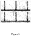
- Figure 9 shows silver interconnects deposited on PMMA for a polymer display application. It illustrates the capability of 3 DTM to deposit and laser-fire conductive inks on low temperature polymer. The silver nanoparticle ink was deposited into 35 micrometres (microns) wide lines on the PMMA. The ink was then allowed to dry for 5 minutes at 80 °C. After drying, a 50 mW, 532nm CW laser was focused onto the deposits and scanned at 20 mm/s in order to sinter the nanoparticles. The measured resistance of 6 cm-long interconnects was 100 Ohms. This corresponds to a resistivity of 16 ⁇ Ohm-cm, which is less than approximately 10x larger than that of bulk silver. The deposits adhered well to the PMMA, passing an adhesive tape test.
Landscapes
- Chemical & Material Sciences (AREA)
- Engineering & Computer Science (AREA)
- Physics & Mathematics (AREA)
- Chemical Kinetics & Catalysis (AREA)
- Organic Chemistry (AREA)
- Health & Medical Sciences (AREA)
- General Chemical & Material Sciences (AREA)
- Materials Engineering (AREA)
- Mechanical Engineering (AREA)
- Metallurgy (AREA)
- Nanotechnology (AREA)
- Polymers & Plastics (AREA)
- Medicinal Chemistry (AREA)
- Toxicology (AREA)
- Theoretical Computer Science (AREA)
- Thermal Sciences (AREA)
- General Engineering & Computer Science (AREA)
- High Energy & Nuclear Physics (AREA)
- Mathematical Physics (AREA)
- Plasma & Fusion (AREA)
- Crystallography & Structural Chemistry (AREA)
- Spectroscopy & Molecular Physics (AREA)
- Optics & Photonics (AREA)
- Manufacturing & Machinery (AREA)
- Electrodes Of Semiconductors (AREA)
- Manufacturing Of Printed Wiring (AREA)
- Application Of Or Painting With Fluid Materials (AREA)
- Other Surface Treatments For Metallic Materials (AREA)
- Thin Film Transistor (AREA)
Claims (28)
- Procédé de dépôt d'un matériau sur une cible, le procédé comprenant les étapes de :génération d'un flux d'aérosol comprenant le matériau ;encerclement du flux d'aérosol avec un gaz d'enveloppe de coécoulement ;chauffage de l'aérosol en vol à l'aide d'un laser jusqu'à une température dépassant une température seuil d'endommagement de la cible ; etdépôt du flux d'aérosol sur la cible à l'aide d'un jet d'aérosol pour former un dépôt comprenant une largeur entre un micromètre (micron) et un millimètre ;dans lequel une propriété électrique résultante du dépôt est sensiblement similaire à une propriété électrique du matériau en vrac.
- Procédé selon la revendication 1, dans lequel la propriété électrique comprend la résistivité.
- Procédé selon la revendication 1, dans lequel la cible est non plane.
- Procédé selon la revendication 1, dans lequel la température seuil d'endommagement est inférieure à 200 °C.
- Procédé selon la revendication 1, dans lequel le flux d'aérosol comprend un ou plusieurs matériaux choisis dans le groupe consistant en des précurseurs chimiques moléculaires liquides, des suspensions colloïdales ou de particules, et un ou plusieurs matériaux générés à partir du groupe consistant en un précurseur métallo-organique ; une solution de métal colloïdale ; une pâte de métal ; une suspension de nanoparticules de métal ; un précurseur de céramique ; une pâte de céramique ; une solution de précurseur de résistor ; une pâte de résistor ; une suspension de semi-conducteur inorganique ; une solution de précurseur polymérique ; une suspension colloïdale de particules de métal, diélectriques ou de résistor ; et toute combinaison de ceux-ci.
- Procédé selon la revendication 1, dans lequel le flux d'aérosol comprend des gouttelettes ou des particules ayant un diamètre inférieur à 10 micromètres (microns).
- Procédé selon la revendication 1, dans lequel l'étape de génération comprend l'utilisation d'une transduction ultrasonique ou d'une aérosolisation pneumatique.
- Procédé selon la revendication 1, dans lequel le jet d'aérosol comprend un écoulement annulaire.
- Procédé selon la revendication 8, dans lequel le jet d'aérosol comprend un écoulement chargé en aérosol intérieur encerclé par un écoulement de gaz d'enveloppe qui confine l'écoulement chargé d'aérosol intérieur.
- Procédé selon la revendication 8, dans lequel l'écoulement annulaire concentre le flux d'aérosol à un diamètre entre 1 et 1 000 micromètres (microns).
- Procédé selon la revendication 10, dans lequel la largeur du dépôt est supérieure ou égale à approximativement quatre micromètres (microns).
- Procédé selon la revendication 1, dans lequel l'étape de dépôt comprend la fourniture d'un mouvement relatif de la cible et du flux d'aérosol.
- Procédé selon la revendication 1, comprenant en outre l'étape de prétraitement du flux d'aérosol avant l'étape de dépôt.
- Procédé selon la revendication 13, dans lequel l'étape de prétraitement comprend un processus choisi dans le groupe consistant en l'humidification du flux d'aérosol, le séchage du flux d'aérosol et le refroidissement du flux d'aérosol.
- Procédé selon la revendication 1, comprenant en outre l'étape de post-traitement du dépôt après l'étape de dépôt.
- Procédé selon la revendication 15, dans lequel l'étape de post-traitement comprend une action choisie dans le groupe consistant en un traitement thermique, une réduction de la pression ambiante, une irradiation avec un rayonnement électromagnétique, et des combinaisons de ceux-ci.
- Procédé selon la revendication 1, dans lequel la largeur du dépôt est approximativement égale à un diamètre d'un faisceau du laser.
- Procédé selon la revendication 1, dans lequel la largeur du dépôt est supérieure à un diamètre d'un faisceau du laser.
- Procédé selon la revendication 1, comprenant en outre le chauffage du matériau pendant l'étape de dépôt.
- Procédé selon la revendication 1, dans lequel l'étape de chauffage comprend au moins un processus choisi dans le groupe consistant en une décomposition chimique, une polymérisation, un frittage et une fusion.
- Procédé selon la revendication 1, dans lequel la cible comprend un matériau choisi dans le groupe consistant en le polycarbonate, le polytéréphtalate d'éthylène, le polyméthacrylate de méthyle, le polytétrafluoroéthylène, le polyester et l'époxy.
- Procédé selon la revendication 1, dans lequel le laser comprend un laser-diode.
- Procédé selon la revendication 1, dans lequel une puissance du laser est d'approximativement 10 milliwatts.
- Procédé selon la revendication 1, dans lequel le laser comprend un mode d'onde continue ou un mode d'onde puisée.
- Procédé selon la revendication 24, dans lequel le laser comprend un mode d'onde pulsée et une énergie du mode d'onde pulsée est de plusieurs microjoules.
- Procédé selon la revendication 1, comprenant en outre la distribution d'un faisceau laser sur la cible à l'aide d'un système de lentilles et de miroirs, d'une fibre optique, ou d'une combinaison de ceux-ci.
- Procédé selon la revendication 1, dans lequel un faisceau du laser est distribué sur la cible séparément du flux d'aérosol.
- Procédé selon la revendication 27, se traduisant par un dépôt par processus en série et un traitement laser.
Applications Claiming Priority (4)
| Application Number | Priority Date | Filing Date | Title |
|---|---|---|---|
| US50649503P | 2003-09-26 | 2003-09-26 | |
| US50875903P | 2003-10-03 | 2003-10-03 | |
| US10/746,646 US20040197493A1 (en) | 1998-09-30 | 2003-12-23 | Apparatus, methods and precision spray processes for direct write and maskless mesoscale material deposition |
| PCT/US2004/031803 WO2005039814A2 (fr) | 2003-09-26 | 2004-09-27 | Traitement au laser pour depot thermosensible a l'echelle mesoscopique |
Publications (3)
| Publication Number | Publication Date |
|---|---|
| EP1670610A2 EP1670610A2 (fr) | 2006-06-21 |
| EP1670610A4 EP1670610A4 (fr) | 2008-09-10 |
| EP1670610B1 true EP1670610B1 (fr) | 2018-05-30 |
Family
ID=34527899
Family Applications (1)
| Application Number | Title | Priority Date | Filing Date |
|---|---|---|---|
| EP04789155.1A Not-in-force EP1670610B1 (fr) | 2003-09-26 | 2004-09-27 | Traitement au laser pour depot thermosensible a l'echelle mesoscopique |
Country Status (4)
| Country | Link |
|---|---|
| EP (1) | EP1670610B1 (fr) |
| JP (1) | JP2007507114A (fr) |
| KR (1) | KR101225200B1 (fr) |
| WO (1) | WO2005039814A2 (fr) |
Cited By (1)
| Publication number | Priority date | Publication date | Assignee | Title |
|---|---|---|---|---|
| EP3256308B1 (fr) * | 2015-02-10 | 2022-12-21 | Optomec, Inc. | Fabrication de structures tridimensionnelles par durcissement en vol d'aérosols |
Families Citing this family (21)
| Publication number | Priority date | Publication date | Assignee | Title |
|---|---|---|---|---|
| US8110247B2 (en) | 1998-09-30 | 2012-02-07 | Optomec Design Company | Laser processing for heat-sensitive mesoscale deposition of oxygen-sensitive materials |
| US7045015B2 (en) | 1998-09-30 | 2006-05-16 | Optomec Design Company | Apparatuses and method for maskless mesoscale material deposition |
| US7674671B2 (en) | 2004-12-13 | 2010-03-09 | Optomec Design Company | Aerodynamic jetting of aerosolized fluids for fabrication of passive structures |
| US7938341B2 (en) | 2004-12-13 | 2011-05-10 | Optomec Design Company | Miniature aerosol jet and aerosol jet array |
| US7959711B2 (en) * | 2006-11-08 | 2011-06-14 | Shell Oil Company | Gas separation membrane system and method of making thereof using nanoscale metal material |
| TWI482662B (zh) | 2007-08-30 | 2015-05-01 | Optomec Inc | 機械上一體式及緊密式耦合之列印頭以及噴霧源 |
| TWI538737B (zh) * | 2007-08-31 | 2016-06-21 | 阿普托麥克股份有限公司 | 材料沉積總成 |
| JP4912991B2 (ja) * | 2007-09-07 | 2012-04-11 | 住友化学株式会社 | 熱電変換素子の製造方法 |
| KR100979677B1 (ko) * | 2008-04-28 | 2010-09-02 | 한국화학연구원 | 에어로졸 젯 인쇄법을 이용한 유기태양전지 광활성층의 제조방법 |
| DE102009007800A1 (de) * | 2009-02-06 | 2010-08-12 | Fraunhofer-Gesellschaft zur Förderung der angewandten Forschung e.V. | Aerosol-Drucker, dessen Verwendung und Verfahren zur Herstellung von Linienunterbrechungen bei kontinuierlichen Aerosol-Druckverfahren |
| KR101084171B1 (ko) * | 2009-08-10 | 2011-11-17 | 삼성모바일디스플레이주식회사 | 유기 발광 디스플레이 장치 및 유기 발광 디스플레이 장치의 제조 방법 |
| WO2012010893A1 (fr) * | 2010-07-21 | 2012-01-26 | Bae Systems Plc | Formation d'éléments fonctionnels ou structuraux par écriture directe sur une surface |
| EP2410077A1 (fr) * | 2010-07-21 | 2012-01-25 | BAE Systems PLC | Formation d'éléments structurels ou fonctionnels d'écriture directe sur une surface |
| EP2598668A1 (fr) * | 2010-07-27 | 2013-06-05 | Husky Injection Molding Systems S.A. | Procédé consistant à convertir une poudre résistive en un élément chauffant fusionné au moyen d'un appareil de dépôt métallique par laser |
| JP5543889B2 (ja) * | 2010-09-30 | 2014-07-09 | 株式会社クラレ | 配線形成方法、及び配線 |
| FR2966062B1 (fr) * | 2010-10-13 | 2015-05-15 | Thales Sa | Procede de depot de nanoparticules sur une surface et appareil de depot de nanoparticules correspondant |
| ITRM20110184A1 (it) | 2011-04-12 | 2012-10-13 | Dyepower | Procedimento di sinterizzazione di formulazioni a base di ossidi metallici. |
| ITRM20110465A1 (it) | 2011-09-08 | 2013-03-09 | Dyepower | Procedimento di fabbricazione dello strato catalitico dei controelettrodi di celle fotoelettrochimiche. |
| WO2014197027A2 (fr) * | 2013-03-14 | 2014-12-11 | Ndsu Research Foundation | Procédé et appareil destinés à l'impression par écriture directe par aérosol |
| US20170348903A1 (en) * | 2015-02-10 | 2017-12-07 | Optomec, Inc. | Fabrication of Three-Dimensional Materials Gradient Structures by In-Flight Curing of Aerosols |
| US10632746B2 (en) | 2017-11-13 | 2020-04-28 | Optomec, Inc. | Shuttering of aerosol streams |
Family Cites Families (14)
| Publication number | Priority date | Publication date | Assignee | Title |
|---|---|---|---|---|
| US4997809A (en) * | 1987-11-18 | 1991-03-05 | International Business Machines Corporation | Fabrication of patterned lines of high Tc superconductors |
| US5614252A (en) * | 1988-12-27 | 1997-03-25 | Symetrix Corporation | Method of fabricating barium strontium titanate |
| US5064684A (en) | 1989-08-02 | 1991-11-12 | Eastman Kodak Company | Waveguides, interferometers, and methods of their formation |
| EP0705483B1 (fr) | 1994-04-25 | 1999-11-24 | Koninklijke Philips Electronics N.V. | Procede de durcissement d'un film |
| US5770272A (en) * | 1995-04-28 | 1998-06-23 | Massachusetts Institute Of Technology | Matrix-bearing targets for maldi mass spectrometry and methods of production thereof |
| US5882722A (en) | 1995-07-12 | 1999-03-16 | Partnerships Limited, Inc. | Electrical conductors formed from mixtures of metal powders and metallo-organic decompositions compounds |
| CA2240625A1 (fr) * | 1995-12-14 | 1997-06-19 | Imperial College Of Science, Technology & Medicine | Depot de films ou de revetement et formation de poudres |
| US5817550A (en) | 1996-03-05 | 1998-10-06 | Regents Of The University Of California | Method for formation of thin film transistors on plastic substrates |
| US6544599B1 (en) * | 1996-07-31 | 2003-04-08 | Univ Arkansas | Process and apparatus for applying charged particles to a substrate, process for forming a layer on a substrate, products made therefrom |
| US6379745B1 (en) | 1997-02-20 | 2002-04-30 | Parelec, Inc. | Low temperature method and compositions for producing electrical conductors |
| US7108894B2 (en) | 1998-09-30 | 2006-09-19 | Optomec Design Company | Direct Write™ System |
| US7045015B2 (en) | 1998-09-30 | 2006-05-16 | Optomec Design Company | Apparatuses and method for maskless mesoscale material deposition |
| US6636676B1 (en) * | 1998-09-30 | 2003-10-21 | Optomec Design Company | Particle guidance system |
| US6642085B1 (en) | 2000-11-03 | 2003-11-04 | The Regents Of The University Of California | Thin film transistors on plastic substrates with reflective coatings for radiation protection |
-
2004
- 2004-09-27 WO PCT/US2004/031803 patent/WO2005039814A2/fr active Application Filing
- 2004-09-27 EP EP04789155.1A patent/EP1670610B1/fr not_active Not-in-force
- 2004-09-27 JP JP2006528312A patent/JP2007507114A/ja active Pending
- 2004-09-27 KR KR1020067005987A patent/KR101225200B1/ko active IP Right Grant
Non-Patent Citations (1)
| Title |
|---|
| None * |
Cited By (1)
| Publication number | Priority date | Publication date | Assignee | Title |
|---|---|---|---|---|
| EP3256308B1 (fr) * | 2015-02-10 | 2022-12-21 | Optomec, Inc. | Fabrication de structures tridimensionnelles par durcissement en vol d'aérosols |
Also Published As
| Publication number | Publication date |
|---|---|
| EP1670610A4 (fr) | 2008-09-10 |
| KR20060096422A (ko) | 2006-09-11 |
| JP2007507114A (ja) | 2007-03-22 |
| EP1670610A2 (fr) | 2006-06-21 |
| WO2005039814A2 (fr) | 2005-05-06 |
| KR101225200B1 (ko) | 2013-01-23 |
| WO2005039814A3 (fr) | 2005-12-29 |
Similar Documents
| Publication | Publication Date | Title |
|---|---|---|
| US7294366B2 (en) | Laser processing for heat-sensitive mesoscale deposition | |
| US8110247B2 (en) | Laser processing for heat-sensitive mesoscale deposition of oxygen-sensitive materials | |
| EP1670610B1 (fr) | Traitement au laser pour depot thermosensible a l'echelle mesoscopique | |
| US7485345B2 (en) | Apparatuses and methods for maskless mesoscale material deposition | |
| US7682970B2 (en) | Maskless nanofabrication of electronic components | |
| US9607889B2 (en) | Forming structures using aerosol jet® deposition | |
| US20040197493A1 (en) | Apparatus, methods and precision spray processes for direct write and maskless mesoscale material deposition | |
| US6805918B2 (en) | Laser forward transfer of rheological systems | |
| WO2006041657A9 (fr) | Gravure directe de cuivre sans masque au moyen d'un jet aerosol annulaire | |
| KR100769636B1 (ko) | 다층구조 형성 방법 | |
| Gibson et al. | Direct write technologies | |
| CN100591428C (zh) | 用于热敏性中等尺度沉积的激光处理 | |
| US20050274772A1 (en) | Treating an area to increase affinity for a fluid | |
| WO2002092674A1 (fr) | Transfert avant par laser de systemes rheologiques | |
| Rahman et al. | Laser direct-write of materials for microelectronics applications | |
| EP3943197A1 (fr) | Dépôt par jet à l'aide d'un aérosol sec produit par laser | |
| Myers et al. | Two-stage silver sintering process improves sheet resistance, film uniformity, and layering properties via electrohydrodynamic jet printing | |
| Alemohammad et al. | Laser assisted maskless microdeposition for conformal direct writing of optical fibers |
Legal Events
| Date | Code | Title | Description |
|---|---|---|---|
| PUAI | Public reference made under article 153(3) epc to a published international application that has entered the european phase |
Free format text: ORIGINAL CODE: 0009012 |
|
| AK | Designated contracting states |
Kind code of ref document: A2 Designated state(s): AT BE BG CH CY CZ DE DK EE ES FI FR GB GR HU IE IT LI LU MC NL PL PT RO SE SI SK TR |
|
| AX | Request for extension of the european patent |
Extension state: AL HR LT LV MK |
|
| 17P | Request for examination filed |
Effective date: 20060629 |
|
| RBV | Designated contracting states (corrected) |
Designated state(s): AT BE BG CH CY CZ DE DK EE ES FI FR GB GR HU IE IT LI LU MC NL PL PT RO SE SI SK TR |
|
| RIC1 | Information provided on ipc code assigned before grant |
Ipc: B05D 1/02 20060101AFI20060824BHEP |
|
| DAX | Request for extension of the european patent (deleted) | ||
| A4 | Supplementary search report drawn up and despatched |
Effective date: 20080811 |
|
| RIC1 | Information provided on ipc code assigned before grant |
Ipc: C23C 18/02 20060101ALI20080805BHEP Ipc: B05D 1/02 20060101AFI20060824BHEP |
|
| STAA | Information on the status of an ep patent application or granted ep patent |
Free format text: STATUS: EXAMINATION IS IN PROGRESS |
|
| 17Q | First examination report despatched |
Effective date: 20170127 |
|
| GRAP | Despatch of communication of intention to grant a patent |
Free format text: ORIGINAL CODE: EPIDOSNIGR1 |
|
| STAA | Information on the status of an ep patent application or granted ep patent |
Free format text: STATUS: GRANT OF PATENT IS INTENDED |
|
| RIC1 | Information provided on ipc code assigned before grant |
Ipc: C23C 18/02 20060101ALI20171215BHEP Ipc: B05D 1/02 20060101AFI20171215BHEP Ipc: B05D 3/06 20060101ALI20171215BHEP Ipc: C23C 18/14 20060101ALI20171215BHEP Ipc: C08F 2/46 20060101ALI20171215BHEP |
|
| INTG | Intention to grant announced |
Effective date: 20180122 |
|
| GRAS | Grant fee paid |
Free format text: ORIGINAL CODE: EPIDOSNIGR3 |
|
| GRAA | (expected) grant |
Free format text: ORIGINAL CODE: 0009210 |
|
| STAA | Information on the status of an ep patent application or granted ep patent |
Free format text: STATUS: THE PATENT HAS BEEN GRANTED |
|
| AK | Designated contracting states |
Kind code of ref document: B1 Designated state(s): AT BE BG CH CY CZ DE DK EE ES FI FR GB GR HU IE IT LI LU MC NL PL PT RO SE SI SK TR |
|
| REG | Reference to a national code |
Ref country code: GB Ref legal event code: FG4D |
|
| REG | Reference to a national code |
Ref country code: CH Ref legal event code: EP |
|
| REG | Reference to a national code |
Ref country code: AT Ref legal event code: REF Ref document number: 1003087 Country of ref document: AT Kind code of ref document: T Effective date: 20180615 |
|
| REG | Reference to a national code |
Ref country code: IE Ref legal event code: FG4D |
|
| REG | Reference to a national code |
Ref country code: DE Ref legal event code: R096 Ref document number: 602004052775 Country of ref document: DE |
|
| REG | Reference to a national code |
Ref country code: FR Ref legal event code: PLFP Year of fee payment: 15 |
|
| REG | Reference to a national code |
Ref country code: NL Ref legal event code: MP Effective date: 20180530 |
|
| PG25 | Lapsed in a contracting state [announced via postgrant information from national office to epo] |
Ref country code: ES Free format text: LAPSE BECAUSE OF FAILURE TO SUBMIT A TRANSLATION OF THE DESCRIPTION OR TO PAY THE FEE WITHIN THE PRESCRIBED TIME-LIMIT Effective date: 20180530 Ref country code: SE Free format text: LAPSE BECAUSE OF FAILURE TO SUBMIT A TRANSLATION OF THE DESCRIPTION OR TO PAY THE FEE WITHIN THE PRESCRIBED TIME-LIMIT Effective date: 20180530 Ref country code: FI Free format text: LAPSE BECAUSE OF FAILURE TO SUBMIT A TRANSLATION OF THE DESCRIPTION OR TO PAY THE FEE WITHIN THE PRESCRIBED TIME-LIMIT Effective date: 20180530 Ref country code: CY Free format text: LAPSE BECAUSE OF FAILURE TO SUBMIT A TRANSLATION OF THE DESCRIPTION OR TO PAY THE FEE WITHIN THE PRESCRIBED TIME-LIMIT Effective date: 20180530 Ref country code: BG Free format text: LAPSE BECAUSE OF FAILURE TO SUBMIT A TRANSLATION OF THE DESCRIPTION OR TO PAY THE FEE WITHIN THE PRESCRIBED TIME-LIMIT Effective date: 20180830 |
|
| PG25 | Lapsed in a contracting state [announced via postgrant information from national office to epo] |
Ref country code: GR Free format text: LAPSE BECAUSE OF FAILURE TO SUBMIT A TRANSLATION OF THE DESCRIPTION OR TO PAY THE FEE WITHIN THE PRESCRIBED TIME-LIMIT Effective date: 20180831 |
|
| REG | Reference to a national code |
Ref country code: AT Ref legal event code: MK05 Ref document number: 1003087 Country of ref document: AT Kind code of ref document: T Effective date: 20180530 |
|
| PG25 | Lapsed in a contracting state [announced via postgrant information from national office to epo] |
Ref country code: NL Free format text: LAPSE BECAUSE OF FAILURE TO SUBMIT A TRANSLATION OF THE DESCRIPTION OR TO PAY THE FEE WITHIN THE PRESCRIBED TIME-LIMIT Effective date: 20180530 |
|
| PG25 | Lapsed in a contracting state [announced via postgrant information from national office to epo] |
Ref country code: SK Free format text: LAPSE BECAUSE OF FAILURE TO SUBMIT A TRANSLATION OF THE DESCRIPTION OR TO PAY THE FEE WITHIN THE PRESCRIBED TIME-LIMIT Effective date: 20180530 Ref country code: DK Free format text: LAPSE BECAUSE OF FAILURE TO SUBMIT A TRANSLATION OF THE DESCRIPTION OR TO PAY THE FEE WITHIN THE PRESCRIBED TIME-LIMIT Effective date: 20180530 Ref country code: EE Free format text: LAPSE BECAUSE OF FAILURE TO SUBMIT A TRANSLATION OF THE DESCRIPTION OR TO PAY THE FEE WITHIN THE PRESCRIBED TIME-LIMIT Effective date: 20180530 Ref country code: PL Free format text: LAPSE BECAUSE OF FAILURE TO SUBMIT A TRANSLATION OF THE DESCRIPTION OR TO PAY THE FEE WITHIN THE PRESCRIBED TIME-LIMIT Effective date: 20180530 Ref country code: AT Free format text: LAPSE BECAUSE OF FAILURE TO SUBMIT A TRANSLATION OF THE DESCRIPTION OR TO PAY THE FEE WITHIN THE PRESCRIBED TIME-LIMIT Effective date: 20180530 Ref country code: RO Free format text: LAPSE BECAUSE OF FAILURE TO SUBMIT A TRANSLATION OF THE DESCRIPTION OR TO PAY THE FEE WITHIN THE PRESCRIBED TIME-LIMIT Effective date: 20180530 Ref country code: CZ Free format text: LAPSE BECAUSE OF FAILURE TO SUBMIT A TRANSLATION OF THE DESCRIPTION OR TO PAY THE FEE WITHIN THE PRESCRIBED TIME-LIMIT Effective date: 20180530 |
|
| PG25 | Lapsed in a contracting state [announced via postgrant information from national office to epo] |
Ref country code: IT Free format text: LAPSE BECAUSE OF FAILURE TO SUBMIT A TRANSLATION OF THE DESCRIPTION OR TO PAY THE FEE WITHIN THE PRESCRIBED TIME-LIMIT Effective date: 20180530 |
|
| REG | Reference to a national code |
Ref country code: DE Ref legal event code: R097 Ref document number: 602004052775 Country of ref document: DE |
|
| PLBE | No opposition filed within time limit |
Free format text: ORIGINAL CODE: 0009261 |
|
| STAA | Information on the status of an ep patent application or granted ep patent |
Free format text: STATUS: NO OPPOSITION FILED WITHIN TIME LIMIT |
|
| PG25 | Lapsed in a contracting state [announced via postgrant information from national office to epo] |
Ref country code: MC Free format text: LAPSE BECAUSE OF FAILURE TO SUBMIT A TRANSLATION OF THE DESCRIPTION OR TO PAY THE FEE WITHIN THE PRESCRIBED TIME-LIMIT Effective date: 20180530 |
|
| REG | Reference to a national code |
Ref country code: CH Ref legal event code: PL |
|
| 26N | No opposition filed |
Effective date: 20190301 |
|
| PG25 | Lapsed in a contracting state [announced via postgrant information from national office to epo] |
Ref country code: SI Free format text: LAPSE BECAUSE OF FAILURE TO SUBMIT A TRANSLATION OF THE DESCRIPTION OR TO PAY THE FEE WITHIN THE PRESCRIBED TIME-LIMIT Effective date: 20180530 |
|
| REG | Reference to a national code |
Ref country code: BE Ref legal event code: MM Effective date: 20180930 |
|
| PG25 | Lapsed in a contracting state [announced via postgrant information from national office to epo] |
Ref country code: LU Free format text: LAPSE BECAUSE OF NON-PAYMENT OF DUE FEES Effective date: 20180927 |
|
| PG25 | Lapsed in a contracting state [announced via postgrant information from national office to epo] |
Ref country code: LI Free format text: LAPSE BECAUSE OF NON-PAYMENT OF DUE FEES Effective date: 20180930 Ref country code: BE Free format text: LAPSE BECAUSE OF NON-PAYMENT OF DUE FEES Effective date: 20180930 Ref country code: CH Free format text: LAPSE BECAUSE OF NON-PAYMENT OF DUE FEES Effective date: 20180930 |
|
| PG25 | Lapsed in a contracting state [announced via postgrant information from national office to epo] |
Ref country code: TR Free format text: LAPSE BECAUSE OF FAILURE TO SUBMIT A TRANSLATION OF THE DESCRIPTION OR TO PAY THE FEE WITHIN THE PRESCRIBED TIME-LIMIT Effective date: 20180530 |
|
| PG25 | Lapsed in a contracting state [announced via postgrant information from national office to epo] |
Ref country code: PT Free format text: LAPSE BECAUSE OF FAILURE TO SUBMIT A TRANSLATION OF THE DESCRIPTION OR TO PAY THE FEE WITHIN THE PRESCRIBED TIME-LIMIT Effective date: 20180530 Ref country code: HU Free format text: LAPSE BECAUSE OF FAILURE TO SUBMIT A TRANSLATION OF THE DESCRIPTION OR TO PAY THE FEE WITHIN THE PRESCRIBED TIME-LIMIT; INVALID AB INITIO Effective date: 20040927 |
|
| PGFP | Annual fee paid to national office [announced via postgrant information from national office to epo] |
Ref country code: IE Payment date: 20210927 Year of fee payment: 18 Ref country code: FR Payment date: 20210927 Year of fee payment: 18 |
|
| PGFP | Annual fee paid to national office [announced via postgrant information from national office to epo] |
Ref country code: GB Payment date: 20210927 Year of fee payment: 18 Ref country code: DE Payment date: 20210929 Year of fee payment: 18 |
|
| REG | Reference to a national code |
Ref country code: DE Ref legal event code: R119 Ref document number: 602004052775 Country of ref document: DE |
|
| GBPC | Gb: european patent ceased through non-payment of renewal fee |
Effective date: 20220927 |
|
| PG25 | Lapsed in a contracting state [announced via postgrant information from national office to epo] |
Ref country code: IE Free format text: LAPSE BECAUSE OF NON-PAYMENT OF DUE FEES Effective date: 20220927 Ref country code: FR Free format text: LAPSE BECAUSE OF NON-PAYMENT OF DUE FEES Effective date: 20220930 Ref country code: DE Free format text: LAPSE BECAUSE OF NON-PAYMENT OF DUE FEES Effective date: 20230401 |
|
| PG25 | Lapsed in a contracting state [announced via postgrant information from national office to epo] |
Ref country code: GB Free format text: LAPSE BECAUSE OF NON-PAYMENT OF DUE FEES Effective date: 20220927 |