EP1670141A2 - Implementierungstechniken von festverdrahteten Decodern in differentiellen Eingangsschaltungen - Google Patents
Implementierungstechniken von festverdrahteten Decodern in differentiellen Eingangsschaltungen Download PDFInfo
- Publication number
- EP1670141A2 EP1670141A2 EP05257487A EP05257487A EP1670141A2 EP 1670141 A2 EP1670141 A2 EP 1670141A2 EP 05257487 A EP05257487 A EP 05257487A EP 05257487 A EP05257487 A EP 05257487A EP 1670141 A2 EP1670141 A2 EP 1670141A2
- Authority
- EP
- European Patent Office
- Prior art keywords
- programmable logic
- differential input
- input buffer
- hardwired
- differential
- Prior art date
- Legal status (The legal status is an assumption and is not a legal conclusion. Google has not performed a legal analysis and makes no representation as to the accuracy of the status listed.)
- Withdrawn
Links
Images


Classifications
-
- H—ELECTRICITY
- H03—ELECTRONIC CIRCUITRY
- H03K—PULSE TECHNIQUE
- H03K19/00—Logic circuits, i.e. having at least two inputs acting on one output; Inverting circuits
- H03K19/02—Logic circuits, i.e. having at least two inputs acting on one output; Inverting circuits using specified components
- H03K19/173—Logic circuits, i.e. having at least two inputs acting on one output; Inverting circuits using specified components using elementary logic circuits as components
- H03K19/177—Logic circuits, i.e. having at least two inputs acting on one output; Inverting circuits using specified components using elementary logic circuits as components arranged in matrix form
- H03K19/17736—Structural details of routing resources
- H03K19/17744—Structural details of routing resources for input/output signals
Definitions
- the present invention relates to techniques for implementing hardwired decoders in differential input circuits, and more particularly, to techniques for decoding differential input signals using hardwired decoders in two adjacent rows/columns of programmable logic elements on a programmable integrated circuit.
- Altera Corporation of San Jose, California is a manufacturer of field programmable gate array (FPGA) devices.
- Stratix® I FPGAs and Stratix II FPGAs are two high end FPGA devices made by Altera.
- Stratix I FPGAs and Stratix II FPGAs contain hardwired (hard) serializer-deserializer (SERDES) and hard double data rate input/output (DDIO) blocks that target high system interface performance.
- SERDES hard serializer-deserializer
- DDIO hard double data rate input/output
- Hard SERDES and hard DDIO blocks provide better timing skew and specifications compared to soft SERDES and soft DDIO blocks.
- the term "soft” refers to building these blocks with programmable logic circuits.
- Hard DDIO and SERDES blocks also have the advantage of having a larger receiver input skew margin.
- Hard SERDES and hard DDIO have not be added to the architecture of Altera's low cost CycloneTM FPGA in order to save die area. Therefore, core programmable logic circuits and programmable interconnect wires are used to build the soft SERDES blocks needed for the low voltage differential signaling standard (LVDS).
- LVDS low voltage differential signaling standard
- Another challenge for implementing the soft solution on an FPGA relates to achieving the necessary maximum clock frequency.
- the LVDS receiver is targeted at 805 Mbps, but the on-chip clock network maximum frequency is only 402.5 MHz.
- Soft DDIO blocks that use a double clocking method are implemented to overcome this problem.
- a double clocking method samples data on both the rising and the falling edges of the clock signal, effectively operating at half the LVDS data rate.
- Stratix FPGAs that use a hard SERDES architecture, a dedicated hard LVDS clock network is implemented to achieve a maximum frequency running at the same frequency as the LVDS data rate.
- Cyclone FPGAs are able to support a LVDS system interface at a high operating frequency by implementing soft DDIO blocks.
- the receiver input skew margin is small in Cyclone FPGAs, because of the delay caused by the programmable logic elements and the programmable interconnect wires. The small receiver input skew margin is not practical for many board designs.
- Each IO decoder in Cyclone FPGAs consists of only three IO registers (on a per port basis).
- the three IO registers are the data-in register, the data-out register, and the output enable register.
- Stratix FPGAs two additional registers are implemented to support hard DDIO blocks in the IO decoder. These two additional registers were removed in Cyclone FPGAs to save die area.
- the edge triggered registers in programmable logic elements are used to build the soft DDIO input registers.
- the input data path from the IO pins travels from an LVDS input buffer through programmable interconnect wires to the edge triggered registers in programmable logic elements.
- the programmable interconnect wires and the edge driven registers that receive signals from one pair of differential IO pins are all in the same row or the same column of programmable logic elements.
- the path through the programmable interconnect wires causes a larger sampling window and a reduced receiver input skew margin for the following reasons.
- the input data path is longer, because the programmable interconnect wires are relatively slow.
- the longer input data path causes a longer propagation delay and increases the setup time (TSU) used to determine the sampling window.
- an input buffer receives differential signals applied to differential input pins.
- the output signals of the input buffer are routed to two hard IO decoder blocks that are located in two adjacent rows/columns of programmable logic elements.
- Each IO decoder block has a data-in register that receives output signals of the differential buffer.
- the data-in registers in two adjacent IO decoder blocks support a double clocking technique.
- IO decoder blocks of the present invention have reduced setup times, hold times, and sampling windows relative to soft DDIO blocks, and have a minimal impact on die area.
- FIG. 1 illustrates a differential input circuitry on a field programmable gate array (FPGA) according to an embodiment of the present invention.
- FPGA field programmable gate array
- Figure 2 illustrates a timing diagram for a prior art differential input circuitry and a timing diagram for the input circuitry of Figure 1.
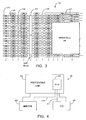
- Figure 3 is a simplified block diagram of a programmable logic device that can be used with the techniques of the present invention.
- FIG. 4 is a block diagram of an electronic system that can implement embodiments of the present invention.
- Figure 1 illustrates input/output (IO) driver blocks, IO decoder blocks, and SERDES blocks in two adjacent rows/columns of logic elements on a field programmable gate array (FPGA) or a programmable logic device (PLD), according to the present invention.
- FPGA field programmable gate array
- PLD programmable logic device
- Two pins 121 and 122 are shown in Figure 1.
- Pins 121 and 122 can be used separately as single ended pins or together as differential pins.
- Single ended input signals are driven by single ended buffer 102 from pin 121 to flip-flop 105.
- Single ended input signals are driven by single ended buffer 103 from pin 122 to flip-flop 106 through demultiplexer 104.
- LVDS input buffer 101 receives differential input signals applied to pins 121 and 122.
- Input buffer 101 drives its output signal to flip-flop 105 and to flip-flop 106 through demultiplexer 104.
- the output signal of buffer 101 is single ended.
- Demultiplexer 104 is a hardwired circuit on the FPGA. Adding one hardwired demultiplexer for each set of differential input pins on the FPGA results in a minimal increase in the die area of the integrated circuit.
- the select input of demultiplexer 104 is controlled by a signal stored in memory 125.
- the signal in memory 125 determines when demultiplexer 104 drives a signal to flip-flop 106 from single ended buffer 103 or from differential buffer 101.
- the signal in memory 125 is also coupled to an input of buffer 101 (e.g., as an enable signal).
- FIG. 1 illustrates two IO decoder blocks in two adjacent rows/columns programmable logic elements.
- Each IO decoder block includes a register.
- the IO decoder block of row/column 0 includes flip-flop 105
- IO decoder block of the row/column 1 includes flip-flop 106.
- Flip-flops 105 and 106 are hardwired into the circuitry of the FPGA.
- Flip-flops 105 and 106 are not soft circuits, because they are not programmable.
- the wires connecting the IO driver blocks to flip-flops 105 and 106 are hardwired and not programmable. These hardwired connections reduce propagation delays.
- the IO decoder blocks are associated with two different rows (or two different columns) of programmable logic blocks/elements, although, flip-flops 105 and 106 are not part of programmable logic blocks/elements.
- the architecture of Figure 1 provides a die saving efficiency relative to the prior art architectures, because the registers used for decoding are spread across two rows/columns of logic. Without demultiplexer 104, output signals of the differential buffer are driven only to registers in one row/column of programmable logic elements. Therefore, the registers used for decoding are all in the row/column that includes the first pin 121, and registers in the adjacent row/column that includes the second input pin 122 are unused.
- Signals are routed from differential input buffer 101 to flip-flops 105/106 in two different rows/columns.
- One of the IO decoder blocks receives even bits from differential input buffer 101, and the second IO decoder block receives odd bits from differential input buffer 101.
- the odd numbered bits are latched by flip-flop 105, and the even numbered bits are latched by flip-flop 106.
- Flip-flop 105 is triggered by falling edges of clock signal CLK1
- flip-flop 106 is triggered by rising edges of clock signal CLK1.
- the IO decoder blocks use a double clocking technique that will now be described.
- the output signal of differential input buffer 101 is continuously applied to the D inputs of both flip-flops 105 and 106 in LVDS mode.
- flip-flop 105 On the falling edges of CLK1, flip-flop 105 passes the output signal of buffer 101 to the input of flip-flop 107.
- flip-flop 106 On the rising edges of CLK1, flip-flop 106 passes the output signal of buffer 101 to the input of flip-flop 108.
- the IO decoder blocks separate the even and odd numbered bits from each other.
- Figure 1 also illustrates serial/deserializer (SERDES) blocks in two adjacent rows/columns of programmable logic elements/blocks.
- SERDES serial/deserializer
- the registers in the SERDES blocks of Figure 1 are implemented in soft programmable logic elements/blocks.
- the SERDES blocks includes 2 serial shift registers that are controlled by clock signal CLK1 and a load signal. Each of the two shift registers includes 7 serially coupled flip-flops.
- Figure 1 illustrates one flip-flop 107 in the first shift register and a flip-flop 108 in the second shift register. The odd numbered bits are shifted into the first shift register including flip-flop 107, and the even numbered bits are shifted into the second shift register including flip-flop 108.
- the odd numbered bits are transferred in parallel from the first serial shift register to a set of parallel registers 110 controlled by clock signal CLK2.
- Parallel registers 110 output the odd numbered bits Data[1, 3, 5, 7, 9, ...] in parallel.
- the even numbered bits are transferred in parallel from the second serial shift register to a set of parallel registers 111, that are also controlled by clock signal CLK2.
- Parallel registers 111 output the even numbered bits Data[0, 2, 4, 6, 8, 10, ...] in parallel.
- Figure 2 has timing diagrams that illustrate differences between the present invention and a prior art soft DDIO block technique.
- Timing diagram 201 and 202 both illustrate signal delays for LVDS IO systems at the receiver that are clocked by an internal clock signal having a period shown at the top of Figure 2.
- the system generating the signals in diagram 201 has soft DDIO blocks that are implemented by registers in programmable logic elements according to the prior art.
- the system generating the signals in diagram 202 has hardwired registers in two IO decoder blocks according to the embodiment of Figure 1.
- the receiver input skew margin (RSKM) for Figure 1 of the present invention is substantially longer than the receiver input skew margin (RSKM) for the prior art (diagram 201). Because the registers in the IO decoder blocks and the interconnections coupled to the registers are hardwired in Figure 1, the setup time (TSU), the hold time (THD), and the sampling window are substantially shorter in a IO block of the present invention.
- timing parameters allow the IO circuitry of Figure 1 to support LVDS input signals at a higher frequency.
- the present invention also provides improved control in terms of less variations in the sampling window and the maximum clock frequency across all of the LVDS channels.
- the present invention saves die size area by implementing a double clocking scheme for a differential IO standard within two IO decoder blocks in two adjacent rows/columns of programmable logic elements. No additional registers need to be added into the IO decoder blocks.
- FIG 3 is a simplified partial block diagram of one example of PLD 300 that can include aspects of the present invention, such as the embodiment of Figure 1.
- PLD 300 is an example of a programmable logic integrated circuit in which techniques of the present invention can be implemented.
- PLD 300 includes a two-dimensional array of programmable logic array blocks (or LABs) 302 that are interconnected by a network of column and row interconnects of varying length and speed.
- LABs 302 include multiple (e.g., 10) logic elements (or LEs).
- An LE is a programmable logic block that provides for efficient implementation of user defined logic functions.
- PLD has numerous logic elements that can be configured to implement various combinatorial and sequential functions.
- the logic elements have access to a programmable interconnect structure.
- the programmable interconnect structure can be programmed to interconnect the logic elements in almost any desired configuration.
- PLD 300 also includes a distributed memory structure including RAM blocks of varying sizes provided throughout the array.
- the RAM blocks include, for example, 512 bit blocks 304, 4K blocks 306, and a block 308 providing 512K bits of RAM.
- These memory blocks can also include shift registers and FIFO buffers.
- PLD 300 further includes digital signal processing (DSP) blocks 310 that can implement, for example, multipliers with add or subtract features.
- DSP digital signal processing
- I/O elements (IOEs) 312 located, in this example, around the periphery of the device support numerous single-ended and differential I/O standards. It is to be understood that PLD 300 is described herein for illustrative purposes only and that the present invention can be implemented in many different types of PLDs, FPGAs, and the like.
- FIG. 4 shows a block diagram of an exemplary digital system 400, within which the present invention can be embodied.
- System 400 can be a programmed digital computer system, digital signal processing system, specialized digital switching network, or other processing system. Moreover, such systems can be designed for a wide variety of applications such as telecommunications systems, automotive systems, control systems, consumer electronics, personal computers, Internet communications and networking, and others. Further, system 400 can be provided on a single board, on multiple boards, or within multiple enclosures.
- System 400 includes a processing unit 402, a memory unit 404 and an I/O unit 406 interconnected together by one or more buses.
- a programmable logic device (PLD) 408 is embedded in processing unit 402.
- PLD 408 can serve many different purposes within the system in Figure 4.
- PLD 408 can, for example, be a logical building block of processing unit 402, supporting its internal and external operations.
- PLD 408 is programmed to implement the logical functions necessary to carry on its particular role in system operation.
- PLD 408 can be specially coupled to memory 404 through connection 410 and to I/O unit 406 through connection 412.
- Processing unit 402 can direct data to an appropriate system component for processing or storage, execute a program stored in memory 404 or receive and transmit data via I/O unit 406, or other similar function.
- Processing unit 402 can be a central processing unit (CPU), microprocessor, floating point coprocessor, graphics coprocessor, hardware controller, microcontroller, programmable logic device programmed for use as a controller, network controller, and the like. Furthermore, in many embodiments, there is often no need for a CPU.
- PLD 408 can control the logical operations of the system.
- PLD 408 acts as a reconfigurable processor, which can be reprogrammed as needed to handle a particular computing task.
- programmable logic device 408 can itself include an embedded microprocessor.
- Memory unit 404 can be a random access memory (RAM), read only memory (ROM), fixed or flexible disk media, PC Card flash disk memory, tape, or any other storage means, or any combination of these storage means.
Landscapes
- Engineering & Computer Science (AREA)
- Physics & Mathematics (AREA)
- Mathematical Physics (AREA)
- Computer Networks & Wireless Communication (AREA)
- Computer Hardware Design (AREA)
- Computing Systems (AREA)
- General Engineering & Computer Science (AREA)
- Logic Circuits (AREA)
Applications Claiming Priority (1)
| Application Number | Priority Date | Filing Date | Title |
|---|---|---|---|
| US11/007,827 US7218141B2 (en) | 2004-12-07 | 2004-12-07 | Techniques for implementing hardwired decoders in differential input circuits |
Publications (2)
| Publication Number | Publication Date |
|---|---|
| EP1670141A2 true EP1670141A2 (de) | 2006-06-14 |
| EP1670141A3 EP1670141A3 (de) | 2008-12-03 |
Family
ID=36081415
Family Applications (1)
| Application Number | Title | Priority Date | Filing Date |
|---|---|---|---|
| EP05257487A Withdrawn EP1670141A3 (de) | 2004-12-07 | 2005-12-06 | Implementierungstechniken von festverdrahteten Decodern in differentiellen Eingangsschaltungen |
Country Status (4)
| Country | Link |
|---|---|
| US (1) | US7218141B2 (de) |
| EP (1) | EP1670141A3 (de) |
| JP (1) | JP4292182B2 (de) |
| CN (1) | CN1787376B (de) |
Cited By (1)
| Publication number | Priority date | Publication date | Assignee | Title |
|---|---|---|---|---|
| CN109189706A (zh) * | 2018-09-28 | 2019-01-11 | 天津市英贝特航天科技有限公司 | 一种基于OpenVPX的多路可编程差分定时接口模块及工作方法 |
Families Citing this family (9)
| Publication number | Priority date | Publication date | Assignee | Title |
|---|---|---|---|---|
| US7587537B1 (en) * | 2007-11-30 | 2009-09-08 | Altera Corporation | Serializer-deserializer circuits formed from input-output circuit registers |
| US7242217B2 (en) * | 2004-12-01 | 2007-07-10 | Altera Corporation | Output reporting techniques for hard intellectual property blocks |
| US7439769B1 (en) | 2007-02-21 | 2008-10-21 | Altera Corporation | Programming logic device and method for programming the same |
| US9819345B2 (en) * | 2014-10-02 | 2017-11-14 | Altera Corporation | Scalable 2.5D interface architecture |
| CN105262658A (zh) * | 2015-10-30 | 2016-01-20 | 北京交控科技有限公司 | 一种交换设备、现场总线拓扑结构及传输数据的方法 |
| CN106326156B (zh) * | 2016-08-30 | 2024-04-05 | 西安翔腾微电子科技有限公司 | 基于自适应波特率的单端口通信处理电路和方法 |
| CN107171661B (zh) * | 2017-05-18 | 2021-03-02 | 青岛海信宽带多媒体技术有限公司 | 引脚复用方法及装置、光模块和通信设备 |
| CN115291949B (zh) * | 2022-09-26 | 2022-12-20 | 中国人民解放军国防科技大学 | 一种面向计算流体力学的加速计算装置和加速计算方法 |
| CN117155372B (zh) * | 2023-09-06 | 2024-02-06 | 苏州异格技术有限公司 | 输入输出驱动器结构、输入输出控制方法及通信系统 |
Family Cites Families (17)
| Publication number | Priority date | Publication date | Assignee | Title |
|---|---|---|---|---|
| US6020759A (en) * | 1997-03-21 | 2000-02-01 | Altera Corporation | Programmable logic array device with random access memory configurable as product terms |
| KR100252057B1 (ko) | 1997-12-30 | 2000-05-01 | 윤종용 | 단일 및 이중 데이터 율 겸용 반도체 메모리 장치 |
| US6150838A (en) * | 1999-02-25 | 2000-11-21 | Xilinx, Inc. | FPGA configurable logic block with multi-purpose logic/memory circuit |
| US6275441B1 (en) * | 1999-06-11 | 2001-08-14 | G-Link Technology | Data input/output system for multiple data rate memory devices |
| US7082126B2 (en) * | 1999-08-04 | 2006-07-25 | International Business Machines Corporation | Fiber channel address blocking |
| US6353334B1 (en) * | 2000-01-27 | 2002-03-05 | Xilinx, Inc. | Circuit for converting a logic signal on an output node to a pair of low-voltage differential signals |
| US6535043B2 (en) | 2000-05-26 | 2003-03-18 | Lattice Semiconductor Corp | Clock signal selection system, method of generating a clock signal and programmable clock manager including same |
| US6650140B2 (en) * | 2001-03-19 | 2003-11-18 | Altera Corporation | Programmable logic device with high speed serial interface circuitry |
| US6686769B1 (en) | 2001-12-14 | 2004-02-03 | Altera Corporation | Programmable I/O element circuit for high speed logic devices |
| US6765408B2 (en) * | 2002-02-11 | 2004-07-20 | Lattice Semiconductor Corporation | Device and method with generic logic blocks |
| US7183796B2 (en) * | 2002-03-18 | 2007-02-27 | Nxp Bv. | Configuration memory implementation for LUT-based reconfigurable logic architectures |
| CN1209874C (zh) * | 2002-12-26 | 2005-07-06 | 威盛电子股份有限公司 | 低电压差动信号传送装置 |
| US6952115B1 (en) * | 2003-07-03 | 2005-10-04 | Lattice Semiconductor Corporation | Programmable I/O interfaces for FPGAs and other PLDs |
| US7254797B2 (en) * | 2004-09-30 | 2007-08-07 | Rambus Inc. | Input/output cells with localized clock routing |
| US7106099B1 (en) * | 2004-10-22 | 2006-09-12 | Xilinx, Inc. | Decision-feedback equalization clocking apparatus and method |
| US7242217B2 (en) * | 2004-12-01 | 2007-07-10 | Altera Corporation | Output reporting techniques for hard intellectual property blocks |
| US7434192B2 (en) * | 2004-12-13 | 2008-10-07 | Altera Corporation | Techniques for optimizing design of a hard intellectual property block for data transmission |
-
2004
- 2004-12-07 US US11/007,827 patent/US7218141B2/en not_active Expired - Fee Related
-
2005
- 2005-12-06 EP EP05257487A patent/EP1670141A3/de not_active Withdrawn
- 2005-12-07 CN CN200510129408.XA patent/CN1787376B/zh not_active Expired - Fee Related
- 2005-12-07 JP JP2005353080A patent/JP4292182B2/ja not_active Expired - Fee Related
Cited By (1)
| Publication number | Priority date | Publication date | Assignee | Title |
|---|---|---|---|---|
| CN109189706A (zh) * | 2018-09-28 | 2019-01-11 | 天津市英贝特航天科技有限公司 | 一种基于OpenVPX的多路可编程差分定时接口模块及工作方法 |
Also Published As
| Publication number | Publication date |
|---|---|
| US7218141B2 (en) | 2007-05-15 |
| US20060119386A1 (en) | 2006-06-08 |
| CN1787376B (zh) | 2010-10-27 |
| JP4292182B2 (ja) | 2009-07-08 |
| CN1787376A (zh) | 2006-06-14 |
| EP1670141A3 (de) | 2008-12-03 |
| JP2006166460A (ja) | 2006-06-22 |
Similar Documents
| Publication | Publication Date | Title |
|---|---|---|
| US5968180A (en) | Data capture circuit for asynchronous data transfer | |
| US8686773B1 (en) | In-system margin measurement circuit | |
| US8571059B1 (en) | Apparatus and methods for serial interfaces with shared datapaths | |
| EP3465911B1 (de) | Datenangesteuerter flipflop mit niedrigem clock power | |
| JP2003157229A (ja) | プログラム可能高速入出力インターフェース | |
| US20120324152A1 (en) | Memory controller with bi-directional buffer for achieving high speed capability and related method thereof | |
| US7218141B2 (en) | Techniques for implementing hardwired decoders in differential input circuits | |
| US8248110B1 (en) | Clock switch-over circuits and methods | |
| US20070236247A1 (en) | Techniques For Providing Flexible On-Chip Termination Control on Integrated Circuits | |
| US10340904B2 (en) | Method and apparatus for phase-aligned 2X frequency clock generation | |
| US7363526B1 (en) | Method for transferring data across different clock domains with selectable delay | |
| US8384460B1 (en) | Techniques for phase adjustment | |
| US8812893B1 (en) | Apparatus and methods for low-skew channel bonding | |
| US9100011B1 (en) | Pipelined direct drive routing fabric | |
| EP1667326B1 (de) | Techniken zur Ausgangssignalsteuerung von Hard Intellectual Property Blöcken | |
| US7245168B2 (en) | Clock selection circuit and digital processing system for reducing glitches | |
| US7990783B1 (en) | Postamble timing for DDR memories | |
| US8699648B1 (en) | Apparatus and methods of receiver offset calibration | |
| US7236010B1 (en) | Reduced area freeze logic for programmable logic blocks | |
| US7196542B1 (en) | Techniques for providing increased flexibility to input/output banks with respect to supply voltages | |
| JP2006166460A5 (de) | ||
| US20020199126A1 (en) | Method and system for reducing the effects of simultaneously switching outputs | |
| US7317644B1 (en) | Signal timing for I/O | |
| US8847626B1 (en) | Circuits and methods for providing clock signals | |
| US9680773B1 (en) | Integrated circuit with dynamically-adjustable buffer space for serial interface |
Legal Events
| Date | Code | Title | Description |
|---|---|---|---|
| PUAI | Public reference made under article 153(3) epc to a published international application that has entered the european phase |
Free format text: ORIGINAL CODE: 0009012 |
|
| AK | Designated contracting states |
Kind code of ref document: A2 Designated state(s): AT BE BG CH CY CZ DE DK EE ES FI FR GB GR HU IE IS IT LI LT LU LV MC NL PL PT RO SE SI SK TR |
|
| AX | Request for extension of the european patent |
Extension state: AL BA HR MK YU |
|
| PUAL | Search report despatched |
Free format text: ORIGINAL CODE: 0009013 |
|
| AK | Designated contracting states |
Kind code of ref document: A3 Designated state(s): AT BE BG CH CY CZ DE DK EE ES FI FR GB GR HU IE IS IT LI LT LU LV MC NL PL PT RO SE SI SK TR |
|
| AX | Request for extension of the european patent |
Extension state: AL BA HR MK YU |
|
| AKX | Designation fees paid | ||
| REG | Reference to a national code |
Ref country code: DE Ref legal event code: 8566 |
|
| STAA | Information on the status of an ep patent application or granted ep patent |
Free format text: STATUS: THE APPLICATION IS DEEMED TO BE WITHDRAWN |
|
| 18D | Application deemed to be withdrawn |
Effective date: 20090604 |