EP1668710B1 - Light emitting diode with porous sic substrate and method for fabricating - Google Patents
Light emitting diode with porous sic substrate and method for fabricating Download PDFInfo
- Publication number
- EP1668710B1 EP1668710B1 EP04788908.4A EP04788908A EP1668710B1 EP 1668710 B1 EP1668710 B1 EP 1668710B1 EP 04788908 A EP04788908 A EP 04788908A EP 1668710 B1 EP1668710 B1 EP 1668710B1
- Authority
- EP
- European Patent Office
- Prior art keywords
- electrolyte
- semiconductor material
- porous layer
- substrate
- reservoir
- Prior art date
- Legal status (The legal status is an assumption and is not a legal conclusion. Google has not performed a legal analysis and makes no representation as to the accuracy of the status listed.)
- Expired - Lifetime
Links
- 239000000758 substrate Substances 0.000 title claims description 60
- 238000000034 method Methods 0.000 title claims description 26
- 239000004065 semiconductor Substances 0.000 claims description 79
- 239000003792 electrolyte Substances 0.000 claims description 73
- 239000000463 material Substances 0.000 claims description 52
- 238000000605 extraction Methods 0.000 claims description 20
- 238000010438 heat treatment Methods 0.000 claims description 7
- 238000005286 illumination Methods 0.000 claims description 5
- HBMJWWWQQXIZIP-UHFFFAOYSA-N silicon carbide Chemical compound [Si+]#[C-] HBMJWWWQQXIZIP-UHFFFAOYSA-N 0.000 description 24
- 229910010271 silicon carbide Inorganic materials 0.000 description 23
- 239000002184 metal Substances 0.000 description 19
- 229910052751 metal Inorganic materials 0.000 description 19
- 230000015572 biosynthetic process Effects 0.000 description 13
- 230000008569 process Effects 0.000 description 9
- 239000004593 Epoxy Substances 0.000 description 7
- 239000011148 porous material Substances 0.000 description 6
- LFQSCWFLJHTTHZ-UHFFFAOYSA-N Ethanol Chemical compound CCO LFQSCWFLJHTTHZ-UHFFFAOYSA-N 0.000 description 5
- 150000004767 nitrides Chemical class 0.000 description 5
- 239000004020 conductor Substances 0.000 description 4
- 230000004907 flux Effects 0.000 description 4
- 230000001681 protective effect Effects 0.000 description 4
- BASFCYQUMIYNBI-UHFFFAOYSA-N platinum Chemical compound [Pt] BASFCYQUMIYNBI-UHFFFAOYSA-N 0.000 description 3
- 235000012431 wafers Nutrition 0.000 description 3
- LDDQLRUQCUTJBB-UHFFFAOYSA-N ammonium fluoride Chemical compound [NH4+].[F-] LDDQLRUQCUTJBB-UHFFFAOYSA-N 0.000 description 2
- 238000002048 anodisation reaction Methods 0.000 description 2
- 230000008901 benefit Effects 0.000 description 2
- 238000010586 diagram Methods 0.000 description 2
- 238000007654 immersion Methods 0.000 description 2
- 238000002955 isolation Methods 0.000 description 2
- 230000007246 mechanism Effects 0.000 description 2
- 230000003287 optical effect Effects 0.000 description 2
- 239000000565 sealant Substances 0.000 description 2
- XLYOFNOQVPJJNP-UHFFFAOYSA-N water Substances O XLYOFNOQVPJJNP-UHFFFAOYSA-N 0.000 description 2
- DDFHBQSCUXNBSA-UHFFFAOYSA-N 5-(5-carboxythiophen-2-yl)thiophene-2-carboxylic acid Chemical compound S1C(C(=O)O)=CC=C1C1=CC=C(C(O)=O)S1 DDFHBQSCUXNBSA-UHFFFAOYSA-N 0.000 description 1
- XUIMIQQOPSSXEZ-UHFFFAOYSA-N Silicon Chemical compound [Si] XUIMIQQOPSSXEZ-UHFFFAOYSA-N 0.000 description 1
- 239000012080 ambient air Substances 0.000 description 1
- 238000007743 anodising Methods 0.000 description 1
- 238000013459 approach Methods 0.000 description 1
- 230000005540 biological transmission Effects 0.000 description 1
- 230000015556 catabolic process Effects 0.000 description 1
- 238000005229 chemical vapour deposition Methods 0.000 description 1
- 238000010168 coupling process Methods 0.000 description 1
- 238000005859 coupling reaction Methods 0.000 description 1
- 239000013078 crystal Substances 0.000 description 1
- 230000000593 degrading effect Effects 0.000 description 1
- 238000005401 electroluminescence Methods 0.000 description 1
- 238000001493 electron microscopy Methods 0.000 description 1
- 238000001941 electron spectroscopy Methods 0.000 description 1
- 238000000572 ellipsometry Methods 0.000 description 1
- 230000002708 enhancing effect Effects 0.000 description 1
- 238000005530 etching Methods 0.000 description 1
- 239000010408 film Substances 0.000 description 1
- 239000007788 liquid Substances 0.000 description 1
- 238000004519 manufacturing process Methods 0.000 description 1
- TWNQGVIAIRXVLR-UHFFFAOYSA-N oxo(oxoalumanyloxy)alumane Chemical compound O=[Al]O[Al]=O TWNQGVIAIRXVLR-UHFFFAOYSA-N 0.000 description 1
- 230000003071 parasitic effect Effects 0.000 description 1
- 229910052697 platinum Inorganic materials 0.000 description 1
- 229920001296 polysiloxane Polymers 0.000 description 1
- 229910021426 porous silicon Inorganic materials 0.000 description 1
- 230000004044 response Effects 0.000 description 1
- 229910052594 sapphire Inorganic materials 0.000 description 1
- 239000010980 sapphire Substances 0.000 description 1
- 229920006395 saturated elastomer Polymers 0.000 description 1
- 238000007789 sealing Methods 0.000 description 1
- 229910052710 silicon Inorganic materials 0.000 description 1
- 239000010703 silicon Substances 0.000 description 1
- 239000007787 solid Substances 0.000 description 1
- 239000000126 substance Substances 0.000 description 1
- 239000010409 thin film Substances 0.000 description 1
Images


Classifications
-
- H—ELECTRICITY
- H10—SEMICONDUCTOR DEVICES; ELECTRIC SOLID-STATE DEVICES NOT OTHERWISE PROVIDED FOR
- H10H—INORGANIC LIGHT-EMITTING SEMICONDUCTOR DEVICES HAVING POTENTIAL BARRIERS
- H10H20/00—Individual inorganic light-emitting semiconductor devices having potential barriers, e.g. light-emitting diodes [LED]
- H10H20/80—Constructional details
- H10H20/81—Bodies
- H10H20/819—Bodies characterised by their shape, e.g. curved or truncated substrates
-
- H—ELECTRICITY
- H01—ELECTRIC ELEMENTS
- H01L—SEMICONDUCTOR DEVICES NOT COVERED BY CLASS H10
- H01L21/00—Processes or apparatus adapted for the manufacture or treatment of semiconductor or solid state devices or of parts thereof
- H01L21/02—Manufacture or treatment of semiconductor devices or of parts thereof
- H01L21/04—Manufacture or treatment of semiconductor devices or of parts thereof the devices having potential barriers, e.g. a PN junction, depletion layer or carrier concentration layer
- H01L21/18—Manufacture or treatment of semiconductor devices or of parts thereof the devices having potential barriers, e.g. a PN junction, depletion layer or carrier concentration layer the devices having semiconductor bodies comprising elements of Group IV of the Periodic Table or AIIIBV compounds with or without impurities, e.g. doping materials
- H01L21/30—Treatment of semiconductor bodies using processes or apparatus not provided for in groups H01L21/20 - H01L21/26
- H01L21/302—Treatment of semiconductor bodies using processes or apparatus not provided for in groups H01L21/20 - H01L21/26 to change their surface-physical characteristics or shape, e.g. etching, polishing, cutting
- H01L21/306—Chemical or electrical treatment, e.g. electrolytic etching
- H01L21/3063—Electrolytic etching
-
- H—ELECTRICITY
- H10—SEMICONDUCTOR DEVICES; ELECTRIC SOLID-STATE DEVICES NOT OTHERWISE PROVIDED FOR
- H10H—INORGANIC LIGHT-EMITTING SEMICONDUCTOR DEVICES HAVING POTENTIAL BARRIERS
- H10H20/00—Individual inorganic light-emitting semiconductor devices having potential barriers, e.g. light-emitting diodes [LED]
- H10H20/80—Constructional details
- H10H20/81—Bodies
- H10H20/817—Bodies characterised by the crystal structures or orientations, e.g. polycrystalline, amorphous or porous
-
- H—ELECTRICITY
- H01—ELECTRIC ELEMENTS
- H01L—SEMICONDUCTOR DEVICES NOT COVERED BY CLASS H10
- H01L2224/00—Indexing scheme for arrangements for connecting or disconnecting semiconductor or solid-state bodies and methods related thereto as covered by H01L24/00
- H01L2224/01—Means for bonding being attached to, or being formed on, the surface to be connected, e.g. chip-to-package, die-attach, "first-level" interconnects; Manufacturing methods related thereto
- H01L2224/10—Bump connectors; Manufacturing methods related thereto
- H01L2224/15—Structure, shape, material or disposition of the bump connectors after the connecting process
- H01L2224/16—Structure, shape, material or disposition of the bump connectors after the connecting process of an individual bump connector
- H01L2224/161—Disposition
- H01L2224/16151—Disposition the bump connector connecting between a semiconductor or solid-state body and an item not being a semiconductor or solid-state body, e.g. chip-to-substrate, chip-to-passive
- H01L2224/16221—Disposition the bump connector connecting between a semiconductor or solid-state body and an item not being a semiconductor or solid-state body, e.g. chip-to-substrate, chip-to-passive the body and the item being stacked
- H01L2224/16245—Disposition the bump connector connecting between a semiconductor or solid-state body and an item not being a semiconductor or solid-state body, e.g. chip-to-substrate, chip-to-passive the body and the item being stacked the item being metallic
-
- H—ELECTRICITY
- H01—ELECTRIC ELEMENTS
- H01L—SEMICONDUCTOR DEVICES NOT COVERED BY CLASS H10
- H01L2924/00—Indexing scheme for arrangements or methods for connecting or disconnecting semiconductor or solid-state bodies as covered by H01L24/00
- H01L2924/10—Details of semiconductor or other solid state devices to be connected
- H01L2924/1015—Shape
- H01L2924/10155—Shape being other than a cuboid
- H01L2924/10158—Shape being other than a cuboid at the passive surface
-
- H—ELECTRICITY
- H10—SEMICONDUCTOR DEVICES; ELECTRIC SOLID-STATE DEVICES NOT OTHERWISE PROVIDED FOR
- H10F—INORGANIC SEMICONDUCTOR DEVICES SENSITIVE TO INFRARED RADIATION, LIGHT, ELECTROMAGNETIC RADIATION OF SHORTER WAVELENGTH OR CORPUSCULAR RADIATION
- H10F77/00—Constructional details of devices covered by this subclass
- H10F77/70—Surface textures, e.g. pyramid structures
Definitions
- This invention relates to semiconductor based light emitters, and more particularly to light emitting diodes comprising an emission region formed on a substrate.
- LEDs Light emitting diodes
- LEDs are an important class of solid state devices that convert electric energy to light and generally comprise an active layer of semiconductor material sandwiched between two oppositely doped layers. When a bias is applied across the doped layers, holes and electrons are injected into the active layer where they recombine to generate light. Light is emitted omnidirectionally from the active layer and from all surfaces of the LED.
- the doped and active layers are typically formed on a substrate that can be made of different materials such as silicon (Si), silicon carbide (SiC), and sapphire (Al 2 O 3 ). SiC wafers are often preferred because they have a much closer crystal lattice match to Group-III nitrides, which results in Group III nitride films of higher quality.
- SiC also has a very high thermal conductivity so that the total output power of Group III nitride devices on SiC is not limited by the thermal resistance of the wafer (as is the case with some devices formed on sapphire or Si). Also, the availability of semi insulating SiC wafers provides the capacity for device isolation and reduced parasitic capacitance that make commercial devices possible. SiC substrates are available from Cree Inc., of Durham, North Carolina and methods for producing them are set forth in the scientific literature as well as in U.S. Patents, Nos. Re. 34,861 ; 4,946,547 ; and 5,200,022 .
- TIR total internal reflection
- LEDs with SiC substrates have relatively low light extraction efficiencies because the high index of refraction of SiC (approximately 2.7) compared to the index of refraction for the surrounding material, such as epoxy (approximately 1.5). This difference results in a small escape cone from which light rays from the active area can transmit from the SiC substrate into the epoxy and ultimately escape from the LED package.
- a LED formed of an emission region on a SiC substrate can not include useful roughened surfaces on the SiC substrate to enhance light extraction.
- the backside surfaces of SiC substrates have been lapped to in an attempt to provide a useful level of roughness, but these attempts have met with limited success and did not result in a LED with significantly enhanced light extraction.
- Porous SiC has been fabricated on n-type 6H-SiC by anodizing the material in HF under UV illumination. [ Shor et al. Direct Observation of Porous SiC Formed by Anodization in HF, Appl. Phys. Lett., Vol. 62, No. 22, May 1993, Pgs. 2636-2638 ]. A blue emitting LED has also been demonstrated having porous SiC as its luminescent layer. [ Mimura et al. Blue Electroluminescence From Porous Silicon Carbide, Appl. Phys. Lett., Vol. 65, No. 26, Dec. 1994, Pgs. 3350-3352 ].
- US-5,376,241 relates to the formation of porous SiC under electro-chemical anodization.
- US-4,056,415 concerns an integrated circuit having a dielectric isolation that is fabricated by growing a double epitaxial layer of N-type semiconductor material onto a P-type substrate.
- the present invention provides a light emitting device according to claim 1, an apparatus for forming a porous layer on the surface of a semiconductor in accordance with claim 4 and a method for forming a porous layer on the surface of a semiconductor in line with claim 7.
- the present invention seeks to provide a method and apparatus for forming a porous layer on the surface of a semiconductor material, with the semiconductor material then being used as a substrate for an LED.
- the porous layer is arranged to improve extraction of the LED light that passes through the substrate.
- An apparatus for forming a porous layer on the surface of a semiconductor according to claim 4 of the present invention comprises an (HF based) electrolyte held in a reservoir.
- the reservoir is arranged to allow the electrolyte to contact one or more surfaces of a layer of semiconductor material.
- the apparatus further comprises a heater for heating the electrolyte, a power source for applying a bias across the electrolyte and the layer of semiconductor material and a cup having one or more holes to allow some of said electrolyte to run out of said cup and contact selectively one or more surfaces of said semiconductor material.
- the bias causes a current to run between the electrolyte and the layer of semiconductor material forming a porous layer on the one or more surfaces in contact with said electrolyte.
- a method for forming a porous layer on the surface of a semiconductor according to claim 7 of the present invention comprises providing an electrolyte and placing the electrolyte in contact with one or more surfaces of a layer of semiconductor material opposite to an emission region of an LED coupled to said semiconductor material.
- the electrolyte is heated and a bias is introduced across the electrolyte and the semiconductor material causing a current to flow between the electrolyte and the semiconductor material, forming a porous layer on the one or more surfaces of the semiconductor material in contact with the electrolyte.
- a light emitting device comprises a substrate having a porous layer and a semiconductor emission region formed on the substrate.
- the emission region is capable of emitting light omnidirectionally in response to a bias, with the porous layer enhancing extraction of the emission region light passing through the substrate.
- FIG. 1 shows one embodiment on an apparatus 10 according to the present invention for forming a porous layer on the surface of a semiconductor material 12, with the apparatus 10 preferably used to form a porous layer on the surface of silicon carbide (SiC).
- the apparatus 10 includes a cup shaped reservoir/housing 14 holding a liquid HF-based electrolyte 16 that can comprise different solutions in different concentrations.
- a suitable solution for the electrolyte 16 comprises ethanol (C 2 H 5 OH) and water, with ethanol in a concentration range of a 10 to 50%.
- Another suitable solution comprises a buffered HF-based electrolyte that provides for a more constant Ph value over time and provides for a solution that is less volatile and less dangerous to work with.
- a preferred buffered HF-based electrolyte comprises ammonium fluoride (NH 4 F) and water, with the NH 4 F having different concentrations such as 20% per volume.
- the semiconductor 12 is arranged adjacent to the bottom surface 17 of the reservoir 14 and the bottom of the reservoir 14 has an opening/hole 18 to allow the HF-based solution to pass out the reservoir 14.
- a watertight seal is provided between the semiconductor 12 and the reservoir's bottom surface 17 around the opening 18 and near the bottom surface's outside edge.
- the seal is preferably provided by an O-ring 20, although other sealing components can be used such as gaskets or sealants such as silicone.
- the reservoir 14 is filled with the HF-based electrolyte 16
- some of the electrolyte passes through the hole 18 and fills the space between the housing 14 and the semiconductor 12.
- the O-ring 20 retains the electrolyte 16 in contact with the top surface of the semiconductor 12 and prevents the electrolyte 16 from leaking past the O-ring 20.
- the apparatus 10 also comprises a cathode 22 that is immersed within the electrolyte 16 from the top of the housing 12.
- the cathode 22 can be made of many different materials that conduct a charge to the electrolyte 16 while at the same time not reacting with or dissolving in the electrolyte 16.
- a preferred material for the cathode 22 is platinum (Pt).
- a first conductor 24 is coupled between the negative terminal of a power source 25 and the cathode 22 so that an electrical signal at the negative terminal passes to the cathode 22.
- a second conductor 26 is coupled between the positive terminal of the power source 25 and the semiconductor 12 so that an electrical signal at the positive terminal passes into the semiconductor 12.
- the power source 25 provides a bias at its positive and negative terminal that is conducted to the cathode 22 and semiconductor material 12. The bias then causes a current to run between the cathode 22 and the semiconductor material 12.
- the reservoir opening 18 should be large enough to allow current to flow between the cathode 22 and the semiconductor 12, with the current passing into the semiconductor 12 across most of its surface that is contact with the electrolyte 16.
- the second conductor 26 should be coupled to the semiconductor 12 in a location that is not in contact with the electrolyte 16 to be sure that the current runs through the semiconductor and not only between the cathode 22 and the second conductor 26.
- Many different power sources can be used in the apparatus 10, with a preferred power source being a precision current-voltage source meter having a computer controlled interface that can provide a pre-set constant current or constant voltage.
- Commercially available power sources can be used such as the Keithley 2400 Source Meter, provided by Keithley Instruments Inc.
- the power source 25 can be set to many different current limits, but the porous layer formation process can be difficult to control if the current limit is set too high, and the process being time consuming if the current limit is set too low.
- a suitable range for the current limits is 0.1 to 100 milli-amps/cm 2 .
- the power source can also be set to many different voltages, with a suitable voltage being 2-3 volts.
- a voltage upper limit can be set to 5 volts to allow for better control of the pore formation process.
- the power source 25 preferably provides a constant current drive density, such as in the range of 0.1 to 100 mA/cm 2 , and allows the voltage to vary to meet that current, with the voltage remaining below the set upper limit.
- Heating of the electrolyte 16 during formation of the porous layer results in a semiconductor surface having superior light extraction characteristics when used as the substrate of an LED, compared to an LED having a substrate with a porous layer formed without electrolyte heating.
- Many different heating mechanisms can be used to heat the electrolyte, such as a commercially available immersion heater 28 or a commercially available hot-plate.
- the electrolyte can be heated to different temperatures during the porous layer formation process, with a suitable temperature range being 40 to 90°C.
- the electrolyte 16 can be illuminated by UV light during the pore formation process, with a suitable UV light source (lamp) providing broadband UV illumination.
- the lamp can be arranged above the electrolyte and directed down to provide the illumination.
- a steering mirror can be arranged above the electrolyte to redirect the lamp light down on the electrolyte 16.
- FIG. 2 shows a flow diagram for one embodiment of a method 30 according to the present invention for forming a porous layer on the surface of a semiconductor material.
- the method 30 can utilize apparatus 10 in the formation process, although other pore formation apparatus can be used.
- a HF based electrolyte is provided that can be a HF based electrolyte or buffered HF based electrolyte described above as electrolyte 16.
- the electrolyte is heated, with suitable methods for heating being an immersion heater or a hot plate.
- the electrolyte is placed in contact with the semiconductor material, such as by providing the electrolyte in a reservoir that has a hole for the electrolyte to pass through and contact the semiconductor.
- a sealant or other retaining means is provided to hold the electrolyte in contact with the semiconductor while not allowing all of the electrolyte to pass out of the reservoir.
- the semiconductor can be placed adjacent to the reservoir hole and an O-ring can be included between the reservoir and semiconductor, around the hole.
- a bias is applied across the electrolyte and the semiconductor, which causes a current to flow between the electrolyte and the semiconductor.
- the current forms a porous layer on the surface(s) of the semiconductor in contact with the electrolyte and the bias is applied until the pores reach the desired depth in the semiconductor.
- the volume of semiconductor material that becomes porous is proportional to the time integrated current applied through the electrolyte; i.e. the total volume of semiconductor material having pores is proportional to the total charge applied to the material through the electrolyte.
- a typical time for applying the bias is in the range of 500-1/500 seconds, although the bias could be applied for more or less time. This typically forms a porous layer that is approximately three (3) microns deep.
- step 40 the bias is removed from the electrolyte and the semiconductor at the end of the formation time and in step 42, the semiconductor is removed from contact with the electrolyte.
- the semiconductor can be used further processed as part of an LED.
- the semiconductor can serve as a substrate, with an LED emission region formed on the surface of the semiconductor opposite the porous layer.
- the porous layer is formed in SiC which can then be used as the substrate for an LED.
- the method 30 can also include the optional step 44 that provides for UV illumination electrolyte during formation of the porous layer.
- FIG. 3 shows one embodiment of an LED package 50 according to the present invention, which includes an LED 52 comprising a substrate 54 having a porous layer 55 to improve light extraction of LED light passing through the substrate 54.
- the substrate 54 can be made of many materials and can be many different thicknesses, with a suitable material being SiC with a thickness range of 125-500 microns.
- the LED 52 comprises a standard emission region 56 formed on the substrate 54 using known processes such as metal-organic chemical vapor deposition (MOCVD). The operational details of conventional LEDs are known and are only briefly discussed.
- MOCVD metal-organic chemical vapor deposition
- the LED's emission region 56 can include an active layer sandwiched between two oppositely doped layers, with the layers having standard thicknesses and the active layer emitting light omnidirectionally when a bias is applied across the oppositely doped layers.
- the layers of the emission region can be made of many different semiconductor material systems such as the Group-III Nitride based material system.
- the LED 52 is arranged in the package 50 in a flip-chip orientation with the substrate 54 being the LED's primary emission surface.
- the LED 52 is flip-chip mounted on first and second metal layer 58a, 58b.
- a first contact 60 is coupled between the first metal layer 58a and one of the oppositely doped layers in the emission region 56 and a second contact 62 is coupled between the second metal layer 58b and the emission region's other doped layer.
- a bias can be applied to the contacts 60, 62 through the first and second metal layers 58a, 58b, and the bias is then conducted through the contact 60, 62 to the oppositely doped layers in the emission region, causing the active layer to emit light.
- a substrate contact 64 can be used to apply a bias to one of the oppositely doped layers.
- the other doped layer is contacted to one of the contacts 60, 62 arranged between the metal layers 58a, 58b and the LED.
- a bias is applied to the LED through contact 64 and one of the metal layers 58a, 58b, and the bias can be conducted to the substrate contact 64 from the other of the metal layers 58a, 58b, through a conductive wire (not shown) that runs from the metal layer 58 to the contact 64.
- the top surface of the metal layers 58a, 58b can also be reflective so that light emitted from the emission region toward the metal layers 58a, 58b is reflected back to contribute to the overall emission of the LED package 50.
- the LED 52 and its contacts can be encased in a clear protective material 66, which is typically a transparent epoxy covering the LED 52 and the top surface of the metal layers 58a, 58b.
- the LED 52 can be mounted on the horizontal base of a "metal cup" that typically has conductive paths (not shown) for applying a bias across the contacts on the emission regions oppositely doped layers.
- the top surface, of the metal cup can also be reflective to reflect light from the emission region such that the light contributes to the light emission of the LED package.
- the substrate 54 comprises a porous layer 55 that, in the flip-chip arrangement of the LED 52 is the top and primary emission surface of the LED 52.
- the porous layer 55 is arranged to enhance the light emission of the LED 52.
- the efficiency of conventional LEDs is limited by their inability to emit all of the light that is generated by the active layer.
- the flip-chip arranged LED is emitting, light reaches the primary emitting substrate surface at many different angles.
- Typical substrate semiconductor materials have a high index of refraction compared to ambient air or encapsulating epoxy. Light traveling from a region having a high index of refraction to a region with a low index of refraction that is within a certain critical angle (relative to the surface normal direction) will cross to the lower index region.
- TIR total internal reflection
- the porous layer 55 improves light extraction of the LED 52 by providing a varying surface that allows light that would otherwise be trapped in the LED 52, by total internal reflection (TIR), to escape from the substrate to contribute to light emission.
- TIR total internal reflection
- the variations in the porous layer increases the chances that the TIR light will reach the substrate surface within the critical angle and will be emitted. For light that does not escape the substrate through the porous layer, the variations of the porous layer reflect the light at different angles, increasing the chances that the light will escape on the next pass.
- porous layer The ability of the porous layer to enhance light extraction will initially increase as its depth increases. However, a point is reached where increases in the depth does not improve light extraction, but may actually reduce it.
- a suitable porous layer depth is approximately three (3) microns. Different porous layer formation processes using different electrolytes can result in different suitable porous layer depths.
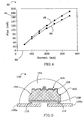
- FIG. 4 is a table 80 comparing the performance of a standard LED package and the performance of an LED package with a porous layer according to the present invention.
- the table 80 plots the current 82 applied to the LEDs verses the light output flux 84 of the LEDs.
- the first plot 86 is for the standard LED and shows that as the current 82 increases the light output flux 84 increases.
- the second plot 88 is for the LED with a porous layer according to the present invention which also shows that as the current 82 increases, the output flux 84 also increases.
- the output flux for the porous layer LED at the same current as a standard LED is generally greater, particularly as the current applied to the LEDs increases past approximately 50 mA.
- FIG. 5 shows another embodiment of an LED package 100 according to the present invention that includes LED 102 that comprises a substrate 104 with a semiconductor emission region 106 formed on one of its surfaces.
- the emission region 106 is similar to emission region 56 in FIG. 3 .
- the LED 102 is mounted on first and second metal layers 108a, 108b having contacts 110, 112 to contact the oppositely doped layers in the emission region 106.
- a bias applied to the metal layers 108a, 108b can be applied to the oppositely doped layers through the contacts 110, 112.
- the LED 102 is flip-chip mounted in such that the substrate's bottom surface is the primary emitting surface of the LED 102.
- the LED 102 can also be encased in a protective transparent epoxy 114.
- the emitting surface of the LED 102 (surface of substrate 104) is not flat, but instead has a sawtooth pattern 105.
- the sawtooth pattern 105 is formed on the substrate 104 using known processes such as etching, and a porous layer 116 is formed in the sawtooth pattern 105.
- the porous layer can be formed using the apparatus 10 and method 30 described above and shown in FIGs. 1 and 2 .
- the sawtooth pattern 105 enhances light extraction by providing a varying surface to allow TIR light to escape from the LED.
- the porous layer 116 in combination with the sawtooth pattern 105 can provide even a greater degree of light extraction compared to a flat substrate surface with the porous layer.
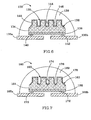
- FIG. 6 shows another embodiment of a LED package 130 according to the present invention also having a flip-chip mounted LED 132 comprising a substrate 134 and an emission region 136.
- the LED 132 is mounted to metal layers 138a, 138b with contacts 140, 142 to apply a bias to the emission region 136.
- the LED 132 is also encased in a protective transparent epoxy 139.
- the emitting surface of the substrate 134 has a trench pattern 135 with each of the trenches having vertical sidewalls 144 and a horizontal bottom surface 146. After formation of the trench pattern 135 on the substrate 134 a porous layer 148 is formed on the trench pattern.
- the trench pattern 135 and porous layer 148 combination provides enhanced light extraction from the LED 132.
- FIG. 7 shows still another embodiment of an LED package 160 according to the present invention also having a flip-chip mounted LED 162 comprising a substrate 164 and an emission region 166.
- the LED 162 is mounted to metal layers 168a, 168b with two contacts 170, 172 to apply a bias to the emission region 166.
- the LED 162 is also encased in a protective transparent epoxy 169.
- the emitting surface of the substrate 164 has a post pattern 165 that is similar to the trench pattern 135 in FIG. 6 .
- Each post has vertical sidewalls 174 but the bottom surface 176 between posts is V-shaped.
- LED packages described above can have different components, such as a metal cup instead of a metal layer.
- Different embodiments of LED packages according to the present invention can have a porous layer in different locations in its LED as long as it falls within the scope of claim 1.
- the substrate can also have many different patterns beyond those described above. The scope of the invention is defined by the terms of the claims.
Landscapes
- Engineering & Computer Science (AREA)
- Physics & Mathematics (AREA)
- Condensed Matter Physics & Semiconductors (AREA)
- General Physics & Mathematics (AREA)
- Manufacturing & Machinery (AREA)
- Computer Hardware Design (AREA)
- Microelectronics & Electronic Packaging (AREA)
- Power Engineering (AREA)
- Led Devices (AREA)
- Led Device Packages (AREA)
- Weting (AREA)
- Formation Of Insulating Films (AREA)
Applications Claiming Priority (2)
| Application Number | Priority Date | Filing Date | Title |
|---|---|---|---|
| US10/676,953 US6972438B2 (en) | 2003-09-30 | 2003-09-30 | Light emitting diode with porous SiC substrate and method for fabricating |
| PCT/US2004/031050 WO2005034254A1 (en) | 2003-09-30 | 2004-09-21 | Light emitting diode with porous sic substrate and method for fabricating |
Publications (2)
| Publication Number | Publication Date |
|---|---|
| EP1668710A1 EP1668710A1 (en) | 2006-06-14 |
| EP1668710B1 true EP1668710B1 (en) | 2014-12-24 |
Family
ID=34422124
Family Applications (1)
| Application Number | Title | Priority Date | Filing Date |
|---|---|---|---|
| EP04788908.4A Expired - Lifetime EP1668710B1 (en) | 2003-09-30 | 2004-09-21 | Light emitting diode with porous sic substrate and method for fabricating |
Country Status (8)
Families Citing this family (59)
| Publication number | Priority date | Publication date | Assignee | Title |
|---|---|---|---|---|
| EP2264798B1 (en) | 2003-04-30 | 2020-10-14 | Cree, Inc. | High powered light emitter packages with compact optics |
| US7005679B2 (en) | 2003-05-01 | 2006-02-28 | Cree, Inc. | Multiple component solid state white light |
| US7534633B2 (en) * | 2004-07-02 | 2009-05-19 | Cree, Inc. | LED with substrate modifications for enhanced light extraction and method of making same |
| US8174037B2 (en) | 2004-09-22 | 2012-05-08 | Cree, Inc. | High efficiency group III nitride LED with lenticular surface |
| JP2006179511A (ja) * | 2004-12-20 | 2006-07-06 | Sumitomo Electric Ind Ltd | 発光装置 |
| EP1969633B1 (en) | 2005-12-22 | 2018-08-29 | Cree, Inc. | Lighting device |
| WO2007081719A2 (en) | 2006-01-05 | 2007-07-19 | Illumitex, Inc. | Separate optical device for directing light from an led |
| KR101198763B1 (ko) * | 2006-03-23 | 2012-11-12 | 엘지이노텍 주식회사 | 기둥 구조와 이를 이용한 발광 소자 및 그 형성방법 |
| US20070241326A1 (en) * | 2006-04-18 | 2007-10-18 | Samsung Electronics Co., Ltd. | Organic light emitting diode display and manufacturing method thereof |
| JP2009538536A (ja) | 2006-05-26 | 2009-11-05 | クリー エル イー ディー ライティング ソリューションズ インコーポレイテッド | 固体発光デバイス、および、それを製造する方法 |
| US8174025B2 (en) * | 2006-06-09 | 2012-05-08 | Philips Lumileds Lighting Company, Llc | Semiconductor light emitting device including porous layer |
| US20080025037A1 (en) * | 2006-07-28 | 2008-01-31 | Visteon Global Technologies, Inc. | LED headlamp |
| JP2010502014A (ja) | 2006-08-23 | 2010-01-21 | クリー エル イー ディー ライティング ソリューションズ インコーポレイテッド | 照明装置、および照明方法 |
| US8087960B2 (en) | 2006-10-02 | 2012-01-03 | Illumitex, Inc. | LED system and method |
| JP4835377B2 (ja) * | 2006-10-20 | 2011-12-14 | 日立電線株式会社 | 半導体発光素子 |
| KR100826412B1 (ko) * | 2006-11-03 | 2008-04-29 | 삼성전기주식회사 | 질화물 반도체 발광 소자 및 제조방법 |
| US8337045B2 (en) * | 2006-12-04 | 2012-12-25 | Cree, Inc. | Lighting device and lighting method |
| EP2095011A1 (en) | 2006-12-04 | 2009-09-02 | Cree Led Lighting Solutions, Inc. | Lighting assembly and lighting method |
| US8021904B2 (en) * | 2007-02-01 | 2011-09-20 | Cree, Inc. | Ohmic contacts to nitrogen polarity GaN |
| US7808657B2 (en) * | 2007-06-28 | 2010-10-05 | International Business Machines Corporation | Wafer and stage alignment using photonic devices |
| EP2171502B1 (en) | 2007-07-17 | 2016-09-14 | Cree, Inc. | Optical elements with internal optical features and methods of fabricating same |
| US11114594B2 (en) | 2007-08-24 | 2021-09-07 | Creeled, Inc. | Light emitting device packages using light scattering particles of different size |
| US8368100B2 (en) * | 2007-11-14 | 2013-02-05 | Cree, Inc. | Semiconductor light emitting diodes having reflective structures and methods of fabricating same |
| US8536584B2 (en) * | 2007-11-14 | 2013-09-17 | Cree, Inc. | High voltage wire bond free LEDS |
| US9634191B2 (en) * | 2007-11-14 | 2017-04-25 | Cree, Inc. | Wire bond free wafer level LED |
| US9431589B2 (en) | 2007-12-14 | 2016-08-30 | Cree, Inc. | Textured encapsulant surface in LED packages |
| US8080849B2 (en) * | 2008-01-17 | 2011-12-20 | International Business Machines Corporation | Characterizing films using optical filter pseudo substrate |
| KR20100122485A (ko) | 2008-02-08 | 2010-11-22 | 일루미텍스, 인크. | 발광체층 쉐이핑을 위한 시스템 및 방법 |
| US8637883B2 (en) * | 2008-03-19 | 2014-01-28 | Cree, Inc. | Low index spacer layer in LED devices |
| TW201034256A (en) | 2008-12-11 | 2010-09-16 | Illumitex Inc | Systems and methods for packaging light-emitting diode devices |
| JP5330880B2 (ja) * | 2009-03-27 | 2013-10-30 | 学校法人 名城大学 | 発光ダイオード素子及びその製造方法 |
| US8476668B2 (en) | 2009-04-06 | 2013-07-02 | Cree, Inc. | High voltage low current surface emitting LED |
| US9093293B2 (en) | 2009-04-06 | 2015-07-28 | Cree, Inc. | High voltage low current surface emitting light emitting diode |
| US8449128B2 (en) | 2009-08-20 | 2013-05-28 | Illumitex, Inc. | System and method for a lens and phosphor layer |
| US8585253B2 (en) | 2009-08-20 | 2013-11-19 | Illumitex, Inc. | System and method for color mixing lens array |
| EP2480816A1 (en) | 2009-09-25 | 2012-08-01 | Cree, Inc. | Lighting device with low glare and high light level uniformity |
| EP3923352A1 (en) * | 2010-01-27 | 2021-12-15 | Yale University, Inc. | Conductivity based selective etch for gan devices and applications thereof |
| US8329482B2 (en) | 2010-04-30 | 2012-12-11 | Cree, Inc. | White-emitting LED chips and method for making same |
| US9070851B2 (en) | 2010-09-24 | 2015-06-30 | Seoul Semiconductor Co., Ltd. | Wafer-level light emitting diode package and method of fabricating the same |
| US8455882B2 (en) | 2010-10-15 | 2013-06-04 | Cree, Inc. | High efficiency LEDs |
| BR112013012333A2 (pt) * | 2010-11-19 | 2019-03-06 | Koninklijke Philips Electronics N.V | método, dispositivo emissor de luz e quadro condutor carregador isolado para dispositivo emissor de luz |
| US10435812B2 (en) | 2012-02-17 | 2019-10-08 | Yale University | Heterogeneous material integration through guided lateral growth |
| WO2014004261A1 (en) | 2012-06-28 | 2014-01-03 | Yale University | Lateral electrochemical etching of iii-nitride materials for microfabrication |
| WO2014030686A1 (ja) * | 2012-08-22 | 2014-02-27 | 住友大阪セメント株式会社 | 色素増感型太陽電池用ペースト、多孔質光反射絶縁層、及び色素増感型太陽電池 |
| US9711352B2 (en) | 2013-03-15 | 2017-07-18 | Yale University | Large-area, laterally-grown epitaxial semiconductor layers |
| CN104241262B (zh) | 2013-06-14 | 2020-11-06 | 惠州科锐半导体照明有限公司 | 发光装置以及显示装置 |
| US9299899B2 (en) | 2013-07-23 | 2016-03-29 | Grote Industries, Llc | Flexible lighting device having unobtrusive conductive layers |
| TWI671800B (zh) | 2014-04-16 | 2019-09-11 | 耶魯大學 | 獲得平面的半極性氮化鎵表面的方法 |
| US11095096B2 (en) | 2014-04-16 | 2021-08-17 | Yale University | Method for a GaN vertical microcavity surface emitting laser (VCSEL) |
| CN106233471A (zh) | 2014-04-16 | 2016-12-14 | 耶鲁大学 | 蓝宝石衬底上的氮‑极性的半极性GaN层和器件 |
| CN107078190B (zh) | 2014-09-30 | 2020-09-08 | 耶鲁大学 | 用于GaN垂直微腔面发射激光器(VCSEL)的方法 |
| US11018231B2 (en) | 2014-12-01 | 2021-05-25 | Yale University | Method to make buried, highly conductive p-type III-nitride layers |
| EP3298624B1 (en) | 2015-05-19 | 2023-04-19 | Yale University | A method and device concerning iii-nitride edge emitting laser diode of high confinement factor with lattice matched cladding layer |
| CN205944139U (zh) | 2016-03-30 | 2017-02-08 | 首尔伟傲世有限公司 | 紫外线发光二极管封装件以及包含此的发光二极管模块 |
| CN109564850A (zh) | 2016-08-12 | 2019-04-02 | 耶鲁大学 | 通过在生长期间消除氮极性小面而在异质衬底上生长的无堆垛层错的半极性和非极性gan |
| KR102391610B1 (ko) | 2017-08-04 | 2022-04-28 | 쑤저우 레킨 세미컨덕터 컴퍼니 리미티드 | 반도체 소자 패키지 및 광원 장치 |
| US11592166B2 (en) | 2020-05-12 | 2023-02-28 | Feit Electric Company, Inc. | Light emitting device having improved illumination and manufacturing flexibility |
| US11876042B2 (en) | 2020-08-03 | 2024-01-16 | Feit Electric Company, Inc. | Omnidirectional flexible light emitting device |
| FR3132593B1 (fr) * | 2022-02-08 | 2025-04-18 | Centre Nat Rech Scient | Creation d’une fenetre de sortie de rayonnement pour un composant photoemetteur |
Citations (4)
| Publication number | Priority date | Publication date | Assignee | Title |
|---|---|---|---|---|
| US4056415A (en) * | 1975-08-04 | 1977-11-01 | International Telephone And Telegraph Corporation | Method for providing electrical isolating material in selected regions of a semiconductive material |
| US5681448A (en) * | 1994-12-27 | 1997-10-28 | Nissan Motor Co., Ltd. | Electrochemical process and system for etching semiconductor substrates |
| US5939732A (en) * | 1997-05-22 | 1999-08-17 | Kulite Semiconductor Products, Inc. | Vertical cavity-emitting porous silicon carbide light-emitting diode device and preparation thereof |
| US6391166B1 (en) * | 1998-02-12 | 2002-05-21 | Acm Research, Inc. | Plating apparatus and method |
Family Cites Families (15)
| Publication number | Priority date | Publication date | Assignee | Title |
|---|---|---|---|---|
| US4866005A (en) | 1987-10-26 | 1989-09-12 | North Carolina State University | Sublimation of silicon carbide to produce large, device quality single crystals of silicon carbide |
| US4946547A (en) | 1989-10-13 | 1990-08-07 | Cree Research, Inc. | Method of preparing silicon carbide surfaces for crystal growth |
| US5200022A (en) | 1990-10-03 | 1993-04-06 | Cree Research, Inc. | Method of improving mechanically prepared substrate surfaces of alpha silicon carbide for deposition of beta silicon carbide thereon and resulting product |
| US5298767A (en) | 1992-10-06 | 1994-03-29 | Kulite Semiconductor Products, Inc. | Porous silicon carbide (SiC) semiconductor device |
| JPH077180A (ja) * | 1993-06-16 | 1995-01-10 | Sanyo Electric Co Ltd | 発光素子 |
| JPH077179A (ja) | 1993-06-16 | 1995-01-10 | Sanyo Electric Co Ltd | 発光素子 |
| JPH08148280A (ja) | 1994-04-14 | 1996-06-07 | Toshiba Corp | 半導体装置およびその製造方法 |
| JP3985065B2 (ja) * | 1997-05-14 | 2007-10-03 | 忠弘 大見 | 多孔質シリコン基板の形成方法及び多孔質シリコン基板の形成装置 |
| US6225647B1 (en) * | 1998-07-27 | 2001-05-01 | Kulite Semiconductor Products, Inc. | Passivation of porous semiconductors for improved optoelectronic device performance and light-emitting diode based on same |
| TW465123B (en) * | 2000-02-02 | 2001-11-21 | Ind Tech Res Inst | High power white light LED |
| CN1252837C (zh) * | 2000-04-26 | 2006-04-19 | 奥斯兰姆奥普托半导体股份有限两合公司 | 在GaN基板上的发光二极管芯片和用GaN基板上的发光二极管芯片制造发光二极管元件的方法 |
| JP3830083B2 (ja) * | 2001-03-07 | 2006-10-04 | スタンレー電気株式会社 | 半導体装置およびその製造方法 |
| JP3802424B2 (ja) * | 2002-01-15 | 2006-07-26 | 株式会社東芝 | 半導体発光素子及びその製造方法 |
| JP3782357B2 (ja) * | 2002-01-18 | 2006-06-07 | 株式会社東芝 | 半導体発光素子の製造方法 |
| JP4590905B2 (ja) * | 2003-10-31 | 2010-12-01 | 豊田合成株式会社 | 発光素子および発光装置 |
-
2003
- 2003-09-30 US US10/676,953 patent/US6972438B2/en not_active Expired - Lifetime
-
2004
- 2004-09-21 CA CA002536154A patent/CA2536154A1/en not_active Abandoned
- 2004-09-21 JP JP2006533962A patent/JP5748384B2/ja not_active Expired - Lifetime
- 2004-09-21 EP EP04788908.4A patent/EP1668710B1/en not_active Expired - Lifetime
- 2004-09-21 WO PCT/US2004/031050 patent/WO2005034254A1/en active Search and Examination
- 2004-09-21 CN CNB2004800279692A patent/CN100470854C/zh not_active Expired - Lifetime
- 2004-09-21 KR KR1020067005898A patent/KR20060090813A/ko not_active Withdrawn
- 2004-09-27 TW TW093129268A patent/TW200518355A/zh unknown
Patent Citations (4)
| Publication number | Priority date | Publication date | Assignee | Title |
|---|---|---|---|---|
| US4056415A (en) * | 1975-08-04 | 1977-11-01 | International Telephone And Telegraph Corporation | Method for providing electrical isolating material in selected regions of a semiconductive material |
| US5681448A (en) * | 1994-12-27 | 1997-10-28 | Nissan Motor Co., Ltd. | Electrochemical process and system for etching semiconductor substrates |
| US5939732A (en) * | 1997-05-22 | 1999-08-17 | Kulite Semiconductor Products, Inc. | Vertical cavity-emitting porous silicon carbide light-emitting diode device and preparation thereof |
| US6391166B1 (en) * | 1998-02-12 | 2002-05-21 | Acm Research, Inc. | Plating apparatus and method |
Also Published As
| Publication number | Publication date |
|---|---|
| US20050184307A1 (en) | 2005-08-25 |
| CA2536154A1 (en) | 2005-04-14 |
| JP2007507895A (ja) | 2007-03-29 |
| JP5748384B2 (ja) | 2015-07-15 |
| KR20060090813A (ko) | 2006-08-16 |
| CN1860619A (zh) | 2006-11-08 |
| CN100470854C (zh) | 2009-03-18 |
| TW200518355A (en) | 2005-06-01 |
| WO2005034254A1 (en) | 2005-04-14 |
| EP1668710A1 (en) | 2006-06-14 |
| US6972438B2 (en) | 2005-12-06 |
Similar Documents
| Publication | Publication Date | Title |
|---|---|---|
| EP1668710B1 (en) | Light emitting diode with porous sic substrate and method for fabricating | |
| KR102171024B1 (ko) | 반도체 발광소자 패키지의 제조 방법 | |
| Huang et al. | Twofold efficiency improvement in high performance AlGaInP light‐emitting diodes in the 555–620 nm spectral region using a thick GaP window layer | |
| KR100872717B1 (ko) | 발광 소자 및 그 제조방법 | |
| US8507941B2 (en) | Ultraviolet light emitting diode with AC voltage operation | |
| US8405068B2 (en) | Reflecting light emitting structure and method of manufacture thereof | |
| US7843133B2 (en) | White light emitting device with particular light emitting structure | |
| US20110180776A1 (en) | Optoelectronic device based on nanowires and corresponding processes | |
| US10312360B2 (en) | Method for producing trench high electron mobility devices | |
| US9660160B2 (en) | Light emitting device | |
| TW201336108A (zh) | 裝置與半導體元件及其形成方法 | |
| TW200818545A (en) | Semiconductor light emitting device including porous layer | |
| US10665759B2 (en) | Reflective structure for light emitting devices | |
| TW201037859A (en) | Light emitting diode chip and manufacturing method thereof | |
| CN110993758B (zh) | 微型发光二极管的显示阵列及其制作方法 | |
| TWI380484B (en) | Light-emitting device, method for making the same, and nitride semiconductor substrate | |
| CN1564331A (zh) | 一种GaN基发光二极管的制作方法 | |
| US20080265272A1 (en) | Light Emitting Device Having Zener Diode Therein And Method Of Fabricating The Same | |
| CN101926002A (zh) | 具有温度补偿的发光单元 | |
| US6596556B2 (en) | Light emitting diode and a method for manufacturing the same | |
| US9312457B2 (en) | Light emitting device and method for manufacturing the same | |
| CN101635324B (zh) | 发光元件及其制造方法 | |
| CN1707820A (zh) | GaN基发光器件制作方法及其器件结构 | |
| KR910006705B1 (ko) | 발광다이오드 어레이 및 그 제조방법 | |
| US20120146069A1 (en) | Oxide Based LED BEOL Integration |
Legal Events
| Date | Code | Title | Description |
|---|---|---|---|
| PUAI | Public reference made under article 153(3) epc to a published international application that has entered the european phase |
Free format text: ORIGINAL CODE: 0009012 |
|
| 17P | Request for examination filed |
Effective date: 20060418 |
|
| AK | Designated contracting states |
Kind code of ref document: A1 Designated state(s): AT BE BG CH CY CZ DE DK EE ES FI FR GB GR HU IE IT LI LU MC NL PL PT RO SE SI SK TR |
|
| 17Q | First examination report despatched |
Effective date: 20060711 |
|
| DAX | Request for extension of the european patent (deleted) | ||
| RIN1 | Information on inventor provided before grant (corrected) |
Inventor name: IBBETSON, JAMES Inventor name: LI, TING Inventor name: KELLER, BERND |
|
| REG | Reference to a national code |
Ref country code: DE Ref legal event code: R079 Ref document number: 602004046396 Country of ref document: DE Free format text: PREVIOUS MAIN CLASS: H01L0033000000 Ipc: H01L0021306300 |
|
| GRAP | Despatch of communication of intention to grant a patent |
Free format text: ORIGINAL CODE: EPIDOSNIGR1 |
|
| RIC1 | Information provided on ipc code assigned before grant |
Ipc: H01L 33/20 20100101ALI20140702BHEP Ipc: H01L 31/0236 20060101ALN20140702BHEP Ipc: H01L 33/16 20100101ALI20140702BHEP Ipc: H01L 21/3063 20060101AFI20140702BHEP |
|
| INTG | Intention to grant announced |
Effective date: 20140714 |
|
| GRAS | Grant fee paid |
Free format text: ORIGINAL CODE: EPIDOSNIGR3 |
|
| GRAA | (expected) grant |
Free format text: ORIGINAL CODE: 0009210 |
|
| AK | Designated contracting states |
Kind code of ref document: B1 Designated state(s): AT BE BG CH CY CZ DE DK EE ES FI FR GB GR HU IE IT LI LU MC NL PL PT RO SE SI SK TR |
|
| REG | Reference to a national code |
Ref country code: GB Ref legal event code: FG4D |
|
| REG | Reference to a national code |
Ref country code: CH Ref legal event code: EP |
|
| REG | Reference to a national code |
Ref country code: IE Ref legal event code: FG4D |
|
| REG | Reference to a national code |
Ref country code: AT Ref legal event code: REF Ref document number: 703519 Country of ref document: AT Kind code of ref document: T Effective date: 20150115 |
|
| REG | Reference to a national code |
Ref country code: DE Ref legal event code: R096 Ref document number: 602004046396 Country of ref document: DE Effective date: 20150219 |
|
| REG | Reference to a national code |
Ref country code: NL Ref legal event code: VDEP Effective date: 20141224 |
|
| PG25 | Lapsed in a contracting state [announced via postgrant information from national office to epo] |
Ref country code: FI Free format text: LAPSE BECAUSE OF FAILURE TO SUBMIT A TRANSLATION OF THE DESCRIPTION OR TO PAY THE FEE WITHIN THE PRESCRIBED TIME-LIMIT Effective date: 20141224 |
|
| PG25 | Lapsed in a contracting state [announced via postgrant information from national office to epo] |
Ref country code: GR Free format text: LAPSE BECAUSE OF FAILURE TO SUBMIT A TRANSLATION OF THE DESCRIPTION OR TO PAY THE FEE WITHIN THE PRESCRIBED TIME-LIMIT Effective date: 20150325 Ref country code: SE Free format text: LAPSE BECAUSE OF FAILURE TO SUBMIT A TRANSLATION OF THE DESCRIPTION OR TO PAY THE FEE WITHIN THE PRESCRIBED TIME-LIMIT Effective date: 20141224 |
|
| REG | Reference to a national code |
Ref country code: AT Ref legal event code: MK05 Ref document number: 703519 Country of ref document: AT Kind code of ref document: T Effective date: 20141224 |
|
| PG25 | Lapsed in a contracting state [announced via postgrant information from national office to epo] |
Ref country code: NL Free format text: LAPSE BECAUSE OF FAILURE TO SUBMIT A TRANSLATION OF THE DESCRIPTION OR TO PAY THE FEE WITHIN THE PRESCRIBED TIME-LIMIT Effective date: 20141224 |
|
| PG25 | Lapsed in a contracting state [announced via postgrant information from national office to epo] |
Ref country code: CZ Free format text: LAPSE BECAUSE OF FAILURE TO SUBMIT A TRANSLATION OF THE DESCRIPTION OR TO PAY THE FEE WITHIN THE PRESCRIBED TIME-LIMIT Effective date: 20141224 Ref country code: SK Free format text: LAPSE BECAUSE OF FAILURE TO SUBMIT A TRANSLATION OF THE DESCRIPTION OR TO PAY THE FEE WITHIN THE PRESCRIBED TIME-LIMIT Effective date: 20141224 Ref country code: RO Free format text: LAPSE BECAUSE OF FAILURE TO SUBMIT A TRANSLATION OF THE DESCRIPTION OR TO PAY THE FEE WITHIN THE PRESCRIBED TIME-LIMIT Effective date: 20141224 Ref country code: EE Free format text: LAPSE BECAUSE OF FAILURE TO SUBMIT A TRANSLATION OF THE DESCRIPTION OR TO PAY THE FEE WITHIN THE PRESCRIBED TIME-LIMIT Effective date: 20141224 Ref country code: ES Free format text: LAPSE BECAUSE OF FAILURE TO SUBMIT A TRANSLATION OF THE DESCRIPTION OR TO PAY THE FEE WITHIN THE PRESCRIBED TIME-LIMIT Effective date: 20141224 |
|
| PG25 | Lapsed in a contracting state [announced via postgrant information from national office to epo] |
Ref country code: AT Free format text: LAPSE BECAUSE OF FAILURE TO SUBMIT A TRANSLATION OF THE DESCRIPTION OR TO PAY THE FEE WITHIN THE PRESCRIBED TIME-LIMIT Effective date: 20141224 Ref country code: PL Free format text: LAPSE BECAUSE OF FAILURE TO SUBMIT A TRANSLATION OF THE DESCRIPTION OR TO PAY THE FEE WITHIN THE PRESCRIBED TIME-LIMIT Effective date: 20141224 |
|
| REG | Reference to a national code |
Ref country code: DE Ref legal event code: R097 Ref document number: 602004046396 Country of ref document: DE |
|
| PG25 | Lapsed in a contracting state [announced via postgrant information from national office to epo] |
Ref country code: DK Free format text: LAPSE BECAUSE OF FAILURE TO SUBMIT A TRANSLATION OF THE DESCRIPTION OR TO PAY THE FEE WITHIN THE PRESCRIBED TIME-LIMIT Effective date: 20141224 |
|
| PLBE | No opposition filed within time limit |
Free format text: ORIGINAL CODE: 0009261 |
|
| STAA | Information on the status of an ep patent application or granted ep patent |
Free format text: STATUS: NO OPPOSITION FILED WITHIN TIME LIMIT |
|
| 26N | No opposition filed |
Effective date: 20150925 |
|
| PG25 | Lapsed in a contracting state [announced via postgrant information from national office to epo] |
Ref country code: IT Free format text: LAPSE BECAUSE OF FAILURE TO SUBMIT A TRANSLATION OF THE DESCRIPTION OR TO PAY THE FEE WITHIN THE PRESCRIBED TIME-LIMIT Effective date: 20141224 |
|
| PG25 | Lapsed in a contracting state [announced via postgrant information from national office to epo] |
Ref country code: SI Free format text: LAPSE BECAUSE OF FAILURE TO SUBMIT A TRANSLATION OF THE DESCRIPTION OR TO PAY THE FEE WITHIN THE PRESCRIBED TIME-LIMIT Effective date: 20141224 |
|
| PG25 | Lapsed in a contracting state [announced via postgrant information from national office to epo] |
Ref country code: LU Free format text: LAPSE BECAUSE OF FAILURE TO SUBMIT A TRANSLATION OF THE DESCRIPTION OR TO PAY THE FEE WITHIN THE PRESCRIBED TIME-LIMIT Effective date: 20150921 Ref country code: MC Free format text: LAPSE BECAUSE OF FAILURE TO SUBMIT A TRANSLATION OF THE DESCRIPTION OR TO PAY THE FEE WITHIN THE PRESCRIBED TIME-LIMIT Effective date: 20141224 |
|
| REG | Reference to a national code |
Ref country code: CH Ref legal event code: PL |
|
| GBPC | Gb: european patent ceased through non-payment of renewal fee |
Effective date: 20150921 |
|
| PG25 | Lapsed in a contracting state [announced via postgrant information from national office to epo] |
Ref country code: BE Free format text: LAPSE BECAUSE OF FAILURE TO SUBMIT A TRANSLATION OF THE DESCRIPTION OR TO PAY THE FEE WITHIN THE PRESCRIBED TIME-LIMIT Effective date: 20141224 |
|
| REG | Reference to a national code |
Ref country code: IE Ref legal event code: MM4A |
|
| REG | Reference to a national code |
Ref country code: FR Ref legal event code: ST Effective date: 20160531 |
|
| PG25 | Lapsed in a contracting state [announced via postgrant information from national office to epo] |
Ref country code: CH Free format text: LAPSE BECAUSE OF NON-PAYMENT OF DUE FEES Effective date: 20150930 Ref country code: LI Free format text: LAPSE BECAUSE OF NON-PAYMENT OF DUE FEES Effective date: 20150930 Ref country code: IE Free format text: LAPSE BECAUSE OF NON-PAYMENT OF DUE FEES Effective date: 20150921 Ref country code: GB Free format text: LAPSE BECAUSE OF NON-PAYMENT OF DUE FEES Effective date: 20150921 |
|
| PG25 | Lapsed in a contracting state [announced via postgrant information from national office to epo] |
Ref country code: FR Free format text: LAPSE BECAUSE OF NON-PAYMENT OF DUE FEES Effective date: 20150930 |
|
| PG25 | Lapsed in a contracting state [announced via postgrant information from national office to epo] |
Ref country code: HU Free format text: LAPSE BECAUSE OF FAILURE TO SUBMIT A TRANSLATION OF THE DESCRIPTION OR TO PAY THE FEE WITHIN THE PRESCRIBED TIME-LIMIT; INVALID AB INITIO Effective date: 20040921 Ref country code: BG Free format text: LAPSE BECAUSE OF FAILURE TO SUBMIT A TRANSLATION OF THE DESCRIPTION OR TO PAY THE FEE WITHIN THE PRESCRIBED TIME-LIMIT Effective date: 20141224 |
|
| PG25 | Lapsed in a contracting state [announced via postgrant information from national office to epo] |
Ref country code: CY Free format text: LAPSE BECAUSE OF FAILURE TO SUBMIT A TRANSLATION OF THE DESCRIPTION OR TO PAY THE FEE WITHIN THE PRESCRIBED TIME-LIMIT Effective date: 20141224 |
|
| PG25 | Lapsed in a contracting state [announced via postgrant information from national office to epo] |
Ref country code: TR Free format text: LAPSE BECAUSE OF FAILURE TO SUBMIT A TRANSLATION OF THE DESCRIPTION OR TO PAY THE FEE WITHIN THE PRESCRIBED TIME-LIMIT Effective date: 20141224 |
|
| PG25 | Lapsed in a contracting state [announced via postgrant information from national office to epo] |
Ref country code: PT Free format text: LAPSE BECAUSE OF FAILURE TO SUBMIT A TRANSLATION OF THE DESCRIPTION OR TO PAY THE FEE WITHIN THE PRESCRIBED TIME-LIMIT Effective date: 20141224 |
|
| P01 | Opt-out of the competence of the unified patent court (upc) registered |
Effective date: 20230530 |
|
| PGFP | Annual fee paid to national office [announced via postgrant information from national office to epo] |
Ref country code: DE Payment date: 20230927 Year of fee payment: 20 |
|
| REG | Reference to a national code |
Ref country code: DE Ref legal event code: R071 Ref document number: 602004046396 Country of ref document: DE |