EP1662283A1 - Herstellungsverfahren für einen filmartigen optischen Wellenleiter - Google Patents
Herstellungsverfahren für einen filmartigen optischen Wellenleiter Download PDFInfo
- Publication number
- EP1662283A1 EP1662283A1 EP05025788A EP05025788A EP1662283A1 EP 1662283 A1 EP1662283 A1 EP 1662283A1 EP 05025788 A EP05025788 A EP 05025788A EP 05025788 A EP05025788 A EP 05025788A EP 1662283 A1 EP1662283 A1 EP 1662283A1
- Authority
- EP
- European Patent Office
- Prior art keywords
- optical
- waveguide
- filmy
- face
- cutting
- Prior art date
- Legal status (The legal status is an assumption and is not a legal conclusion. Google has not performed a legal analysis and makes no representation as to the accuracy of the status listed.)
- Granted
Links
- 230000003287 optical effect Effects 0.000 title claims abstract description 98
- 238000000034 method Methods 0.000 title claims abstract description 33
- 238000005520 cutting process Methods 0.000 claims abstract description 36
- 238000004080 punching Methods 0.000 claims abstract description 13
- 239000010410 layer Substances 0.000 description 26
- 239000012792 core layer Substances 0.000 description 20
- 229920001721 polyimide Polymers 0.000 description 19
- 239000009719 polyimide resin Substances 0.000 description 19
- 230000005540 biological transmission Effects 0.000 description 9
- 239000011347 resin Substances 0.000 description 8
- 229920005989 resin Polymers 0.000 description 8
- 239000002243 precursor Substances 0.000 description 7
- 230000000052 comparative effect Effects 0.000 description 6
- 239000010432 diamond Substances 0.000 description 6
- 229910003460 diamond Inorganic materials 0.000 description 6
- 239000000243 solution Substances 0.000 description 6
- 239000003822 epoxy resin Substances 0.000 description 5
- 238000004519 manufacturing process Methods 0.000 description 5
- 229920000647 polyepoxide Polymers 0.000 description 5
- LFQSCWFLJHTTHZ-UHFFFAOYSA-N Ethanol Chemical compound CCO LFQSCWFLJHTTHZ-UHFFFAOYSA-N 0.000 description 4
- 239000000758 substrate Substances 0.000 description 4
- WGTYBPLFGIVFAS-UHFFFAOYSA-M tetramethylammonium hydroxide Chemical compound [OH-].C[N+](C)(C)C WGTYBPLFGIVFAS-UHFFFAOYSA-M 0.000 description 4
- 239000007864 aqueous solution Substances 0.000 description 3
- 230000015572 biosynthetic process Effects 0.000 description 3
- 238000011161 development Methods 0.000 description 3
- 238000004891 communication Methods 0.000 description 2
- 238000001035 drying Methods 0.000 description 2
- 238000010438 heat treatment Methods 0.000 description 2
- 230000010365 information processing Effects 0.000 description 2
- 238000011835 investigation Methods 0.000 description 2
- 239000000463 material Substances 0.000 description 2
- 238000005259 measurement Methods 0.000 description 2
- 229920005575 poly(amic acid) Polymers 0.000 description 2
- 238000012545 processing Methods 0.000 description 2
- 239000002904 solvent Substances 0.000 description 2
- 239000004820 Pressure-sensitive adhesive Substances 0.000 description 1
- 150000001298 alcohols Chemical class 0.000 description 1
- 239000012298 atmosphere Substances 0.000 description 1
- 238000005253 cladding Methods 0.000 description 1
- 239000011247 coating layer Substances 0.000 description 1
- 230000009025 developmental regulation Effects 0.000 description 1
- -1 e.g. Substances 0.000 description 1
- 230000000694 effects Effects 0.000 description 1
- 239000011521 glass Substances 0.000 description 1
- 230000001771 impaired effect Effects 0.000 description 1
- 239000004850 liquid epoxy resins (LERs) Substances 0.000 description 1
- 239000000203 mixture Substances 0.000 description 1
- 238000012986 modification Methods 0.000 description 1
- 230000004048 modification Effects 0.000 description 1
- 239000012299 nitrogen atmosphere Substances 0.000 description 1
- 239000002245 particle Substances 0.000 description 1
- 239000010453 quartz Substances 0.000 description 1
- 230000001105 regulatory effect Effects 0.000 description 1
- 229910052710 silicon Inorganic materials 0.000 description 1
- 239000010703 silicon Substances 0.000 description 1
- VYPSYNLAJGMNEJ-UHFFFAOYSA-N silicon dioxide Inorganic materials O=[Si]=O VYPSYNLAJGMNEJ-UHFFFAOYSA-N 0.000 description 1
- 229910001220 stainless steel Inorganic materials 0.000 description 1
- 239000010935 stainless steel Substances 0.000 description 1
- 238000012360 testing method Methods 0.000 description 1
- 239000002966 varnish Substances 0.000 description 1
Images



Classifications
-
- G—PHYSICS
- G02—OPTICS
- G02B—OPTICAL ELEMENTS, SYSTEMS OR APPARATUS
- G02B6/00—Light guides; Structural details of arrangements comprising light guides and other optical elements, e.g. couplings
- G02B6/10—Light guides; Structural details of arrangements comprising light guides and other optical elements, e.g. couplings of the optical waveguide type
- G02B6/12—Light guides; Structural details of arrangements comprising light guides and other optical elements, e.g. couplings of the optical waveguide type of the integrated circuit kind
- G02B6/13—Integrated optical circuits characterised by the manufacturing method
-
- G—PHYSICS
- G02—OPTICS
- G02B—OPTICAL ELEMENTS, SYSTEMS OR APPARATUS
- G02B6/00—Light guides; Structural details of arrangements comprising light guides and other optical elements, e.g. couplings
- G02B6/10—Light guides; Structural details of arrangements comprising light guides and other optical elements, e.g. couplings of the optical waveguide type
- G02B6/12—Light guides; Structural details of arrangements comprising light guides and other optical elements, e.g. couplings of the optical waveguide type of the integrated circuit kind
- G02B6/122—Basic optical elements, e.g. light-guiding paths
- G02B6/1221—Basic optical elements, e.g. light-guiding paths made from organic materials
-
- G—PHYSICS
- G02—OPTICS
- G02B—OPTICAL ELEMENTS, SYSTEMS OR APPARATUS
- G02B6/00—Light guides; Structural details of arrangements comprising light guides and other optical elements, e.g. couplings
- G02B6/10—Light guides; Structural details of arrangements comprising light guides and other optical elements, e.g. couplings of the optical waveguide type
- G02B6/12—Light guides; Structural details of arrangements comprising light guides and other optical elements, e.g. couplings of the optical waveguide type of the integrated circuit kind
- G02B2006/12133—Functions
- G02B2006/12147—Coupler
-
- G—PHYSICS
- G02—OPTICS
- G02B—OPTICAL ELEMENTS, SYSTEMS OR APPARATUS
- G02B6/00—Light guides; Structural details of arrangements comprising light guides and other optical elements, e.g. couplings
- G02B6/10—Light guides; Structural details of arrangements comprising light guides and other optical elements, e.g. couplings of the optical waveguide type
- G02B6/12—Light guides; Structural details of arrangements comprising light guides and other optical elements, e.g. couplings of the optical waveguide type of the integrated circuit kind
- G02B2006/12133—Functions
- G02B2006/1215—Splitter
-
- G—PHYSICS
- G02—OPTICS
- G02B—OPTICAL ELEMENTS, SYSTEMS OR APPARATUS
- G02B6/00—Light guides; Structural details of arrangements comprising light guides and other optical elements, e.g. couplings
- G02B6/10—Light guides; Structural details of arrangements comprising light guides and other optical elements, e.g. couplings of the optical waveguide type
- G02B6/12—Light guides; Structural details of arrangements comprising light guides and other optical elements, e.g. couplings of the optical waveguide type of the integrated circuit kind
- G02B2006/12166—Manufacturing methods
- G02B2006/1219—Polymerisation
Definitions
- the present invention relates to a process for producing a filmy optical waveguide for extensive use in optical communication, optical information processing, and other general optical fields.
- Optical waveguides are incorporated in optical devices such as optical waveguide devices, optical integrated circuits and optical wiring boards, and are in extensive use in optical communication, optical information processing and other general optical fields.
- the optical waveguides includes filmy ones having a three-layer structure comprising an undercladding layer, a core layer formed thereon which has a predetermined pattern, and an overcladding layer which surrounds the core layer.
- Such filmy optical waveguides are usually obtained from a filmy structure having optical-waveguide parts formed therein, by cutting each optical-waveguide part out of the filmy structure with a diamond blade (rotating blade containing fine diamond particles dispersed therein).
- the optical-waveguide parts each are cut out together with the substrate by means of a diamond blade to thereby form optical waveguides (see, for example, patent document 1).
- Patent Document 1 JP 2003-172839 A
- the cutting with a diamond blade has a drawback that it is difficult to secure the smoothness of the cut surfaces.
- the optical waveguide has impaired light loss characteristics and comes to have a trouble concerning light transmission.
- the filmy optical waveguides are praised because they are flexible and can be incorporated into various optical devices.
- the filmy optical waveguides are required to have a contour (cut surfaces in plan view) which includes a curved or polygonal line or the like according to the shapes of optical devices, etc.
- the diamond blade is a rotating blade, it is applicable only to linear cutting.
- the only way of obtaining the contour including a curved line or the like is to employ another cutting technique. Because of this, the process for producing filmy optical waveguides in which optical-waveguide parts each are cut out with a diamond blade has poor production efficiency.
- the present inventors hence attempted a method of cutting by punching with a die.
- the light entrance end faces and light emission end faces made by such cutting could not have sufficiently improved smoothness although the production efficiency was improved.
- the present invention has been made in view of the foregoing circumstances.
- an object of the invention is to provide a process for filmy-optical-waveguide production by which filmy optical waveguides showing satisfactory light transmission can be efficiently produced.
- the present invention provides a process for producing a filmy optical waveguide from a filmy structure having one or more optical-waveguide parts formed therein, which process comprises:
- filmy optical waveguide as used herein means a thin-film-form multilayer structure having a constitution comprising a core layer which transmits light and a cladding layer which has a lower refractive index than the core layer and surrounds the core layer.
- light entrance end face means one end face of an optical waveguide through which light enters the waveguide
- light emission end face means the other end face(s) of the optical waveguide through which light is emitted from the waveguide.
- the inventors further made extensive investigations on a process for efficiently producing a filmy optical waveguide showing satisfactory light transmission. Namely, investigations were made on a method for cutting a filmy structure having one or more optical-waveguide parts formed therein so as to cut out each of the optical-waveguide parts. As a result, it was found that when cutting for making a light entrance end face and a light emission end face is conducted with a laser light, then the resultant cut surfaces are in a neatly finished state and have sufficiently improved smoothness and the optical waveguide obtained shows satisfactory light transmission.
- waveguide side faces when cutting for making the cut surfaces other than the light entrance end face and light emission end face (such cut surfaces are hereinafter referred to as "waveguide side faces") is conducted by punching with a die, the cutting for making the waveguide side faces can be easily conducted even when the contour of the waveguide side faces includes a curved or polygonal line or the like in a plan view thereof.
- a combination of the cutting with a laser light and the punching with a die secures both the formation of highly precise cut surfaces and the high productivity of optical waveguides, whereby the invention has been achieved.
- the cutting for making a light entrance end face and a light emission end face is conducted with a laser light and the cutting for making waveguide side faces is conducted by punching with a die. Because of this, filmy optical waveguides showing satisfactory light transmission can be efficiently produced.
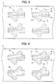
- a filmy structure F having optical-waveguide parts B formed therein is cut in such a manner that the faces serving as waveguide side faces 5 to 8 of each optical waveguide A (see Fig. 7) are made by punching with a die and the faces serving as a light entrance end face 1 and light emission end faces 2 to 4 of the optical waveguide A (see Fig. 7) are made by cutting with a laser light to thereby obtain a filmy optical waveguide A (see Fig. 8).
- the procedure is as follows. First, the filmy structure F having optical-waveguide parts B formed therein (see Fig. 5) is produced.
- This filmy structure F can be produced by a process heretofore in use. Namely, a polyimide resin film for use as an undercladding layer 21 (see Fig. 1) is prepared first. It is preferred that this polyimide resin film have been wound into a roll and be used while being unwound from the roll, so that the subsequent steps of producing the filmy structure F and of cutting out optical-waveguide parts B can be continuously conducted.
- the thickness of the polyimide resin film (undercladding layer 21) is generally in the range of 1-30 ⁇ m, and is preferably in the range of 5-15 ⁇ m.
- a photosensitive polyimide resin precursor solution (photosensitive poly(amic acid) varnish) which is a material giving a layer having a higher refractive index than the polyimide resin film (undercladding layer 21) is applied on the above-mentioned polyimide resin film (undercladding layer 21) in such an amount as to result in a film thickness after drying of generally 2-30 ⁇ m, preferably 6-10 ⁇ m, as shown in Fig. 1.
- This coating layer is predried to form a photosensitive polyimide resin precursor layer 22a which becomes a core layer 22 later (see Fig. 3).
- a photomask M is placed over the photosensitive polyimide resin precursor layer 22a so as to obtain a desired pattern in each optical-waveguide part B (see Fig. 4), and irradiation with ultraviolet L is carried out onto the layer 22a from above the photomask M as shown in Fig. 2.
- the exposure amount in the irradiation with ultraviolet L is 5-50 mJ/cm 2 , sufficient resolution can be attained.
- the heat treatment after exposure which is called post exposure bake (PEB) is conducted in order to complete the photoreaction, and then development with a developing solution (wet processing technique) is conducted.
- a heat treatment is usually conducted in order to imidize the desired pattern thus obtained through the development.
- This treatment is performed at a temperature of generally 300-400°C to conduct solvent removal and curing reaction (cure) under vacuum or in a nitrogen atmosphere.
- a patterned core layer 22 made of a polyimide resin is formed as shown in Fig. 3.
- the developing solution for use in the development is not particularly limited. However, for example, an alkaline aqueous solution of an alcohols is used. More specifically, it is preferred to use a mixed aqueous solution of tetramethylammonium hydroxide and ethanol from the standpoints of satisfactory resolution and ease of the regulation of development rate.
- the proportion of tetramethylammonium hydroxide and that of ethanol are preferably regulated so as to be in the ranges of 2-10% by weight and 40-50% by weight, respectively.
- a polyimide resin precursor solution which is a layer-forming material giving a layer having a lower refractive index than the core layer 22 is applied over the core layer 22 in such an amount as to result in a maximum layer thickness after drying of generally 1-30 ⁇ m, preferably 5-15 ⁇ m, and then dried to thereby form a resin layer comprising a polyimide resin precursor composition, as shown in Fig. 4.
- This resin layer is subsequently heated in an inert atmosphere to thereby complete removal of the solvent remaining in the resin layer and imidization of the polyimide resin precursor.
- an overcladding layer 23 made of a polyimide resin is formed so as to surround the core layer 22. In the manner described above, each optical-waveguide part B is formed.
- each optical-waveguide part B has a pattern in which a light which has entered from one side (left side in Fig. 5) is separated so as to be transmitted in difficult three directions (upper rightward, rightward, and lower rightward directions in Fig. 5).
- one end face 11 left end face in Fig. 5 makes, by cutting, a light entrance end face 1 of an optical waveguide A (see Fig. 7), while front end faces 12 to 14 which are the front ends in the different three directions make, by cutting, light emission end faces 2 to 4 of the optical waveguide A (see Fig. 7).
- each optical-waveguide part B which are located along the pattern of the core layer 22 make, by cutting, waveguide side faces 5 to 8 of the optical waveguide A (see Fig. 7).
- the core layer 22 is formed so as to slightly protrude from the cut surfaces (end face 11 and front end faces 12 to 14).
- the optical-waveguide parts B are then cut by a specific method. Namely, each optical-waveguide part B in the filmy structure F is cut along the side faces 15 to 18 by punching with a die to make the waveguide side faces 5 to 8 of an optical waveguide A (see Fig. 7) as shown in Fig. 6.
- the optical-waveguide part B can be easily cut out even when the contour of the cut surfaces (waveguide side faces 5 to 8) includes a nonlinear part such as a polygonal line in a plan view thereof. Consequently, high productivity of optical waveguides A can be secured.
- each optical-waveguide part B is cut along the end face 11 (left end face in Fig. 6) with a laser light to make the light entrance end face 1 of an optical waveguide A as shown in Fig. 7. Furthermore, the optical-waveguide part B is cut along the front end faces (other end faces) 12 to 14 (see Fig. 6), which are the front ends in the different three directions, with a laser light to make the light emission end faces 2 to 4 of the optical waveguide A. As a result, end parts of the light-transmitting core layer 22 are cut and the light entrance end face 1 and the light emission end faces 2 to 4 have exposed ends of the core layer 22. In the manner described above, optical waveguides A such as those shown in Fig. 8 are obtained.
- the cutting with a laser light enables the cut surfaces (light entrance end face 1 and light emission end faces 2 to 4) to be neat and have sufficiently improved smoothness (gives highly precise cut surfaces), whereby the optical waveguides A obtained show satisfactory light transmission.
- the laser light is not particularly limited, examples thereof include excimer laser lights.
- a polyimide resin film is used as the undercladding layer 21 in producing the filmy structure F.
- a film of another resin such as, e.g., an epoxy resin film may be used in place of the polyimide resin film.
- each optical-waveguide part B is cut out in the embodiment described above, the cutting is conducted in such a manner that the faces serving as the waveguide side faces 5 to 8 of an optical waveguide A are made prior to making the face serving as the light entrance end face 1 of the optical waveguide A and the faces serving as the light emission end faces 2 to 4 thereof.
- this order of cutting may be reversed. Namely, cutting may be conducted in such a manner that the face serving as the light entrance end face 1 and the faces serving as the light emission end faces 2 to 4 are made before the faces serving as the waveguide side faces 5 to 8 are made.
- a filmy structure F having two or more optical-waveguide parts B is produced in the embodiment described above, the filmy structure may have only one optical-waveguide part B.
- Examples of the filmy optical waveguides A thus obtained include straight optical waveguides, bend optical waveguides, crossing optical waveguides, Y-branched optical waveguides, slab optical waveguides, Mach-Zehnder type optical waveguides, grating optical waveguides, and optical waveguide lenses.
- Examples of optical devices employing such optical waveguides include wavelength filters, optical switches, optical branch units, optical multiplexers, optical multiplexers/demultiplexers, optical amplifiers, wavelength modulators, wavelength division multiplexers, optical splitters, directional couplers, opto-electric hybrid circuit boards, and optical transmission modules having a laser diode or photodiode hybrid-integrated therewith.
- the filmy structure shown in Fig. 5 was produced in the manner shown below and optical waveguides were then produced in the manner shown below.
- a strip-form epoxy resin film (width, 250 mm; length, 30 m; thickness, 30 ⁇ m; refractive index, 1.55) for use as an undercladding layer was prepared.
- a core layer having a predetermined pattern (line width, 50 ⁇ m; height, 50 ⁇ m; refractive index, 1.62) was formed from a photosensitive epoxy resin in those areas in the resin film in which optical-waveguide parts were to be formed.
- a liquid epoxy resin was applied over the core layer and then cured to form an overcladding layer (thickness, 30 ⁇ m; refractive index, 1.55).
- a strip-form filmy structure (thickness, 150 ⁇ m) having optical-waveguide parts formed therein was produced.
- each optical-waveguide part in the filmy structure was cut along side faces thereof by punching with a die to thereby make waveguide side faces of an optical waveguide. Subsequently, each optical-waveguide part was cut along one end face thereof with a laser light to make a light entrance end face of the optical waveguide, and further cut along the front end faces in the different three directions with a laser light to make light emission end faces of the optical waveguide. Thus, optical waveguides were obtained.
- Example 2 The same procedure as in Example 1 was conducted, except that the cutting of the optical-waveguide parts in forming optical waveguides was conducted wholly by punching with a die.
- Example 1 and Comparative Example 1 were examined for light loss at the time when a laser light having a wavelength of 850 nm was caused to enter through the light entrance end face.
- the light loss of the optical waveguides of Example 1 and that of the optical waveguides of Comparative Example 1 were found to be 1.5 dB and 30 dB, respectively. Namely, filmy optical waveguides showing satisfactory light transmission could be obtained in Example 1.
- a strip-form fluorinated polyimide resin film (width, 250 mm; length, 30 m; thickness, 20 ⁇ m; refractive index, 1.51) for use as an undercladding layer was prepared.
- a core layer having a predetermined pattern (line width, 8 ⁇ m; height, 8 ⁇ m; refractive index, 1.54) was formed from a photosensitive polyimide resin in those areas in the resin film in which optical-waveguide parts were to be formed.
- a poly(amic acid) solution (polyimide resin precursor solution) was applied over the core layer and then imidized to form an overcladding layer (thickness, 20 ⁇ m; refractive index, 1.51) made of a polyimide resin.
- a strip-form filmy structure (thickness, 48 ⁇ m) having optical-waveguide parts formed therein was produced.
- Optical waveguides were obtained in the same manner as in Example 1.
- Example 2 The same procedure as in Example 2 was conducted, except that the cutting of the optical-waveguide parts in forming optical waveguides was conducted wholly by punching with a die.
- the filmy optical waveguides of Example 2 and Comparative Example 2 thus obtained were examined for light loss at the time when a laser light having a wavelength of 1,550 nm was caused to enter through the light entrance end face.
- the light loss of the optical waveguides of Example 2 and that of the optical waveguides of Comparative Example 2 were found to be 3 dB and 40 dB, respectively. Namely, filmy optical waveguides showing satisfactory light transmission could be obtained in Example 2.
Landscapes
- Physics & Mathematics (AREA)
- Engineering & Computer Science (AREA)
- Microelectronics & Electronic Packaging (AREA)
- General Physics & Mathematics (AREA)
- Optics & Photonics (AREA)
- Optical Integrated Circuits (AREA)
Applications Claiming Priority (1)
| Application Number | Priority Date | Filing Date | Title |
|---|---|---|---|
| JP2004346499A JP2006154447A (ja) | 2004-11-30 | 2004-11-30 | フィルム状光導波路の製法 |
Publications (2)
| Publication Number | Publication Date |
|---|---|
| EP1662283A1 true EP1662283A1 (de) | 2006-05-31 |
| EP1662283B1 EP1662283B1 (de) | 2008-03-12 |
Family
ID=35741406
Family Applications (1)
| Application Number | Title | Priority Date | Filing Date |
|---|---|---|---|
| EP05025788A Expired - Lifetime EP1662283B1 (de) | 2004-11-30 | 2005-11-25 | Herstellungsverfahren für einen filmartigen optischen Wellenleiter |
Country Status (6)
| Country | Link |
|---|---|
| US (1) | US20060120681A1 (de) |
| EP (1) | EP1662283B1 (de) |
| JP (1) | JP2006154447A (de) |
| KR (1) | KR100872244B1 (de) |
| CN (1) | CN1782758A (de) |
| DE (1) | DE602005005268T2 (de) |
Families Citing this family (21)
| Publication number | Priority date | Publication date | Assignee | Title |
|---|---|---|---|---|
| JP4589293B2 (ja) * | 2006-11-13 | 2010-12-01 | 日東電工株式会社 | 光導波路の製造方法 |
| JP2009025385A (ja) | 2007-07-17 | 2009-02-05 | Nitto Denko Corp | フィルム状光導波路の製造方法 |
| JP5101345B2 (ja) * | 2008-03-04 | 2012-12-19 | 日東電工株式会社 | 光導波路装置の製造方法 |
| WO2010016136A1 (ja) * | 2008-08-07 | 2010-02-11 | 富士通株式会社 | フィルム基材の加工方法及びフィルム基材の加工装置 |
| US8905610B2 (en) | 2009-01-26 | 2014-12-09 | Flex Lighting Ii, Llc | Light emitting device comprising a lightguide film |
| US9651729B2 (en) | 2010-04-16 | 2017-05-16 | Flex Lighting Ii, Llc | Reflective display comprising a frontlight with extraction features and a light redirecting optical element |
| US9028123B2 (en) | 2010-04-16 | 2015-05-12 | Flex Lighting Ii, Llc | Display illumination device with a film-based lightguide having stacked incident surfaces |
| CA2829388C (en) | 2011-03-09 | 2018-09-25 | Flex Lighting Ii, Llc | Light emitting device with adjustable light output profile |
| US9566751B1 (en) * | 2013-03-12 | 2017-02-14 | Flex Lighting Ii, Llc | Methods of forming film-based lightguides |
| US11009646B2 (en) | 2013-03-12 | 2021-05-18 | Azumo, Inc. | Film-based lightguide with interior light directing edges in a light mixing region |
| US9690032B1 (en) | 2013-03-12 | 2017-06-27 | Flex Lighting Ii Llc | Lightguide including a film with one or more bends |
| JP7021887B2 (ja) * | 2016-09-30 | 2022-02-17 | 住友化学株式会社 | 光学フィルムの製造方法 |
| JP7112838B2 (ja) * | 2016-09-30 | 2022-08-04 | 住友化学株式会社 | 光学フィルム及びそれを用いた積層フィルム、並びに光学フィルムの製造方法 |
| JP6183531B1 (ja) * | 2016-11-24 | 2017-08-23 | 住友ベークライト株式会社 | 光導波路樹脂フィルムの製造方法および光学部品の製造方法 |
| JP6183530B1 (ja) * | 2016-11-24 | 2017-08-23 | 住友ベークライト株式会社 | 光導波路フィルムおよび光学部品 |
| WO2020047340A1 (en) | 2018-08-30 | 2020-03-05 | Flex Lighting Ii, Llc | Film-based frontlight with angularly varying diffusion film |
| CN113678034B (zh) | 2018-12-11 | 2024-03-19 | 阿祖莫公司 | 使用基于薄膜的光导和漫反射型剥离衬制造显示器的方法 |
| CN113678035B (zh) | 2019-01-03 | 2024-10-18 | 阿祖莫公司 | 包括产生多个照明峰值的光导和光转向膜的反射型显示器 |
| WO2020146668A1 (en) | 2019-01-09 | 2020-07-16 | Flex Lighting Ii, Llc | Reflective display comprising coupling lightguides folded at different fold angles |
| US11513274B2 (en) | 2019-08-01 | 2022-11-29 | Azumo, Inc. | Lightguide with a light input edge between lateral edges of a folded strip |
| WO2022072386A1 (en) | 2020-09-29 | 2022-04-07 | Azumo, Inc | Manufacturing a lightguide with cut lateral edges |
Citations (3)
| Publication number | Priority date | Publication date | Assignee | Title |
|---|---|---|---|---|
| EP0523514A1 (de) * | 1991-07-09 | 1993-01-20 | Hoechst Aktiengesellschaft | Verfahren zur Herstellung eines planaren optischen Kopplers |
| US5195162A (en) * | 1987-12-16 | 1993-03-16 | General Motors Corporation | Planar polymer light guide methods and apparatus |
| US6341190B1 (en) * | 1993-10-01 | 2002-01-22 | Epigem Limited | Organic optical components and preparation thereof |
Family Cites Families (2)
| Publication number | Priority date | Publication date | Assignee | Title |
|---|---|---|---|---|
| US6210514B1 (en) * | 1998-02-11 | 2001-04-03 | Xerox Corporation | Thin film structure machining and attachment |
| JP2004300231A (ja) * | 2003-03-31 | 2004-10-28 | Nitto Denko Corp | 熱剥離性両面粘着シート、被着体の加工方法および電子部品 |
-
2004
- 2004-11-30 JP JP2004346499A patent/JP2006154447A/ja active Pending
-
2005
- 2005-11-25 DE DE602005005268T patent/DE602005005268T2/de not_active Expired - Lifetime
- 2005-11-25 EP EP05025788A patent/EP1662283B1/de not_active Expired - Lifetime
- 2005-11-29 KR KR1020050114927A patent/KR100872244B1/ko not_active Expired - Fee Related
- 2005-11-30 US US11/289,563 patent/US20060120681A1/en not_active Abandoned
- 2005-11-30 CN CN200510127071.9A patent/CN1782758A/zh active Pending
Patent Citations (3)
| Publication number | Priority date | Publication date | Assignee | Title |
|---|---|---|---|---|
| US5195162A (en) * | 1987-12-16 | 1993-03-16 | General Motors Corporation | Planar polymer light guide methods and apparatus |
| EP0523514A1 (de) * | 1991-07-09 | 1993-01-20 | Hoechst Aktiengesellschaft | Verfahren zur Herstellung eines planaren optischen Kopplers |
| US6341190B1 (en) * | 1993-10-01 | 2002-01-22 | Epigem Limited | Organic optical components and preparation thereof |
Also Published As
| Publication number | Publication date |
|---|---|
| KR20060060610A (ko) | 2006-06-05 |
| JP2006154447A (ja) | 2006-06-15 |
| KR100872244B1 (ko) | 2008-12-05 |
| US20060120681A1 (en) | 2006-06-08 |
| EP1662283B1 (de) | 2008-03-12 |
| DE602005005268T2 (de) | 2009-03-05 |
| CN1782758A (zh) | 2006-06-07 |
| DE602005005268D1 (de) | 2008-04-24 |
Similar Documents
| Publication | Publication Date | Title |
|---|---|---|
| EP1662283B1 (de) | Herstellungsverfahren für einen filmartigen optischen Wellenleiter | |
| US7050691B2 (en) | Optical waveguide and method of manufacturing the same | |
| EP0782714B1 (de) | Verfahren zur herstellung eines optischen wellenleiterbauteils | |
| US5850498A (en) | Low stress optical waveguide having conformal cladding and fixture for precision optical interconnects | |
| CN103777275B (zh) | 提供绝热耦合的聚合物波导阵列和硅波导阵列的对准 | |
| JPH01287605A (ja) | 光ファイバコネクタアセンブリおよび該アセンブリの製造方法 | |
| WO1998045736A1 (en) | Raised rib waveguide ribbon for precision optical interconnects | |
| KR20020039336A (ko) | 광섬유 스플라이싱용 중합체 그리핑 소자 | |
| CN100472257C (zh) | 制备光学波导的方法 | |
| US20030235369A1 (en) | Alignment apparatus and methods for transverse optical coupling | |
| JP2000047044A (ja) | 光信号伝送システムおよびその製造方法 | |
| US6816653B2 (en) | Passive alignment of optical fibers with optical elements | |
| JPH1048443A (ja) | ポリマ導波路及びその製造方法 | |
| KR20000011817A (ko) | 광도파로및그제조방법 | |
| Barry et al. | Highly efficient coupling between single-mode fiber and polymer optical waveguides | |
| Li et al. | Self-aligned ormosil waveguide devices | |
| JP2003222747A (ja) | 光回路基板 | |
| JP4458328B2 (ja) | 光導波路の製法 | |
| JP2006018110A (ja) | 光導波路 | |
| JP2004347944A (ja) | 光デバイスおよびその製造方法 | |
| JPH0763936A (ja) | プラスチック導波路型光素子の作製方法 | |
| JP2000310722A (ja) | 光導波路部品の製造方法 | |
| JPH10504913A (ja) | 自立の可撓性導波体シートを用いて、光導波体をファイバーコンベクターにする方法 |
Legal Events
| Date | Code | Title | Description |
|---|---|---|---|
| PUAI | Public reference made under article 153(3) epc to a published international application that has entered the european phase |
Free format text: ORIGINAL CODE: 0009012 |
|
| AK | Designated contracting states |
Kind code of ref document: A1 Designated state(s): AT BE BG CH CY CZ DE DK EE ES FI FR GB GR HU IE IS IT LI LT LU LV MC NL PL PT RO SE SI SK TR |
|
| AX | Request for extension of the european patent |
Extension state: AL BA HR MK YU |
|
| 17P | Request for examination filed |
Effective date: 20061005 |
|
| 17Q | First examination report despatched |
Effective date: 20061201 |
|
| AKX | Designation fees paid |
Designated state(s): DE FR GB |
|
| GRAP | Despatch of communication of intention to grant a patent |
Free format text: ORIGINAL CODE: EPIDOSNIGR1 |
|
| RTI1 | Title (correction) |
Free format text: PROCESS FOR PRODUCING A FILM OPTICAL WAVEGUIDE |
|
| GRAS | Grant fee paid |
Free format text: ORIGINAL CODE: EPIDOSNIGR3 |
|
| GRAA | (expected) grant |
Free format text: ORIGINAL CODE: 0009210 |
|
| AK | Designated contracting states |
Kind code of ref document: B1 Designated state(s): DE FR GB |
|
| REG | Reference to a national code |
Ref country code: GB Ref legal event code: FG4D |
|
| REF | Corresponds to: |
Ref document number: 602005005268 Country of ref document: DE Date of ref document: 20080424 Kind code of ref document: P |
|
| EN | Fr: translation not filed | ||
| PLBE | No opposition filed within time limit |
Free format text: ORIGINAL CODE: 0009261 |
|
| STAA | Information on the status of an ep patent application or granted ep patent |
Free format text: STATUS: NO OPPOSITION FILED WITHIN TIME LIMIT |
|
| 26N | No opposition filed |
Effective date: 20081215 |
|
| PG25 | Lapsed in a contracting state [announced via postgrant information from national office to epo] |
Ref country code: FR Free format text: LAPSE BECAUSE OF FAILURE TO SUBMIT A TRANSLATION OF THE DESCRIPTION OR TO PAY THE FEE WITHIN THE PRESCRIBED TIME-LIMIT Effective date: 20090102 |
|
| PGFP | Annual fee paid to national office [announced via postgrant information from national office to epo] |
Ref country code: DE Payment date: 20121121 Year of fee payment: 8 |
|
| PGFP | Annual fee paid to national office [announced via postgrant information from national office to epo] |
Ref country code: GB Payment date: 20121121 Year of fee payment: 8 |
|
| GBPC | Gb: european patent ceased through non-payment of renewal fee |
Effective date: 20131125 |
|
| REG | Reference to a national code |
Ref country code: DE Ref legal event code: R119 Ref document number: 602005005268 Country of ref document: DE Effective date: 20140603 |
|
| PG25 | Lapsed in a contracting state [announced via postgrant information from national office to epo] |
Ref country code: DE Free format text: LAPSE BECAUSE OF NON-PAYMENT OF DUE FEES Effective date: 20140603 |
|
| PG25 | Lapsed in a contracting state [announced via postgrant information from national office to epo] |
Ref country code: GB Free format text: LAPSE BECAUSE OF NON-PAYMENT OF DUE FEES Effective date: 20131125 |