EP1659638B1 - MOS-Leistungsanordnung und entsprechendes Herstellungsverfahren - Google Patents
MOS-Leistungsanordnung und entsprechendes Herstellungsverfahren Download PDFInfo
- Publication number
- EP1659638B1 EP1659638B1 EP05025288A EP05025288A EP1659638B1 EP 1659638 B1 EP1659638 B1 EP 1659638B1 EP 05025288 A EP05025288 A EP 05025288A EP 05025288 A EP05025288 A EP 05025288A EP 1659638 B1 EP1659638 B1 EP 1659638B1
- Authority
- EP
- European Patent Office
- Prior art keywords
- conductive
- gate
- portions
- layer
- mos device
- Prior art date
- Legal status (The legal status is an assumption and is not a legal conclusion. Google has not performed a legal analysis and makes no representation as to the accuracy of the status listed.)
- Expired - Lifetime
Links
Images


Classifications
-
- H—ELECTRICITY
- H10—SEMICONDUCTOR DEVICES; ELECTRIC SOLID-STATE DEVICES NOT OTHERWISE PROVIDED FOR
- H10D—INORGANIC ELECTRIC SEMICONDUCTOR DEVICES
- H10D30/00—Field-effect transistors [FET]
- H10D30/60—Insulated-gate field-effect transistors [IGFET]
- H10D30/64—Double-diffused metal-oxide semiconductor [DMOS] FETs
- H10D30/66—Vertical DMOS [VDMOS] FETs
-
- H—ELECTRICITY
- H10—SEMICONDUCTOR DEVICES; ELECTRIC SOLID-STATE DEVICES NOT OTHERWISE PROVIDED FOR
- H10D—INORGANIC ELECTRIC SEMICONDUCTOR DEVICES
- H10D30/00—Field-effect transistors [FET]
- H10D30/01—Manufacture or treatment
- H10D30/021—Manufacture or treatment of FETs having insulated gates [IGFET]
- H10D30/028—Manufacture or treatment of FETs having insulated gates [IGFET] of double-diffused metal oxide semiconductor [DMOS] FETs
- H10D30/0291—Manufacture or treatment of FETs having insulated gates [IGFET] of double-diffused metal oxide semiconductor [DMOS] FETs of vertical DMOS [VDMOS] FETs
-
- H—ELECTRICITY
- H10—SEMICONDUCTOR DEVICES; ELECTRIC SOLID-STATE DEVICES NOT OTHERWISE PROVIDED FOR
- H10D—INORGANIC ELECTRIC SEMICONDUCTOR DEVICES
- H10D64/00—Electrodes of devices having potential barriers
- H10D64/20—Electrodes characterised by their shapes, relative sizes or dispositions
- H10D64/27—Electrodes not carrying the current to be rectified, amplified, oscillated or switched, e.g. gates
- H10D64/311—Gate electrodes for field-effect devices
- H10D64/411—Gate electrodes for field-effect devices for FETs
- H10D64/511—Gate electrodes for field-effect devices for FETs for IGFETs
- H10D64/517—Gate electrodes for field-effect devices for FETs for IGFETs characterised by the conducting layers
- H10D64/518—Gate electrodes for field-effect devices for FETs for IGFETs characterised by the conducting layers characterised by their lengths or sectional shapes
-
- H—ELECTRICITY
- H10—SEMICONDUCTOR DEVICES; ELECTRIC SOLID-STATE DEVICES NOT OTHERWISE PROVIDED FOR
- H10D—INORGANIC ELECTRIC SEMICONDUCTOR DEVICES
- H10D64/00—Electrodes of devices having potential barriers
- H10D64/20—Electrodes characterised by their shapes, relative sizes or dispositions
- H10D64/27—Electrodes not carrying the current to be rectified, amplified, oscillated or switched, e.g. gates
- H10D64/311—Gate electrodes for field-effect devices
- H10D64/411—Gate electrodes for field-effect devices for FETs
- H10D64/511—Gate electrodes for field-effect devices for FETs for IGFETs
- H10D64/517—Gate electrodes for field-effect devices for FETs for IGFETs characterised by the conducting layers
- H10D64/519—Gate electrodes for field-effect devices for FETs for IGFETs characterised by the conducting layers characterised by their top-view geometrical layouts
-
- H10D64/0133—
-
- H—ELECTRICITY
- H10—SEMICONDUCTOR DEVICES; ELECTRIC SOLID-STATE DEVICES NOT OTHERWISE PROVIDED FOR
- H10D—INORGANIC ELECTRIC SEMICONDUCTOR DEVICES
- H10D64/00—Electrodes of devices having potential barriers
- H10D64/20—Electrodes characterised by their shapes, relative sizes or dispositions
- H10D64/27—Electrodes not carrying the current to be rectified, amplified, oscillated or switched, e.g. gates
- H10D64/311—Gate electrodes for field-effect devices
- H10D64/411—Gate electrodes for field-effect devices for FETs
- H10D64/511—Gate electrodes for field-effect devices for FETs for IGFETs
- H10D64/514—Gate electrodes for field-effect devices for FETs for IGFETs characterised by the insulating layers
- H10D64/516—Gate electrodes for field-effect devices for FETs for IGFETs characterised by the insulating layers the thicknesses being non-uniform
Definitions
- the present invention relates to a power MOS device, of the type comprising a very high integration of elementary MOS transistors and used in multiple applications both at low and high supply voltage.
- the invention also relates to a method for realising the power MOS device.
- MOS devices in fact require the possibility of operating, both at low supply voltage (20-100V) and at high supply voltage(200-1000V), but, however, at higher and higher frequencies next to the megahertz (MHz).
- Power devices are thus subjected to very high voltage and current gradients during the transients and/or during the switches which make the stresses to the device weakening the same burdensome and reduce its activity period in a drastic way.
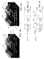
- elementary MOS transistors are realised on semiconductor with polygonal cells or strips and they comprise a body region, which, in the case shown, is of the p type, formed on a suitable substrate, of the n type, and with a source region realised on top.
- the body region together with the source region, forms a channel region covered by an insulating layer, for example a silicon oxide, and by a conductive layer, for example suitably doped polysilicon.
- an insulating layer for example a silicon oxide
- a conductive layer for example suitably doped polysilicon.
- These two insulating and conductive layers represent, for each elementary MOS transistor, the gate dielectric and for the power MOS device they form a biasing mesh also called gate mesh.
- the gate mesh is connected to a terminal called gate pad and it allows to distribute the signals inside the MOS device as well as to turn on and/or off all the elementary MOS transistors composing the power MOS device.
- a DMOS transistor device described in the US patent No. US 5,510,281 issued on April 23, 1996 to Ghezzo et al. (General Electric Company) comprises gate structures having a gate oxide with a thick central part in direct contact with lateral portions of reduced thickness
- the gate mesh due to the high polysilicon resistivity (> 10 Ohm/ [square] ), exhibits resistive contributions along the path which depend on the relative position with respect to the gate pad, as highlighted in the circuit of figure 2 , this implies that gate resistance value of each elementary transistor also depends on the distance from the gate pad.
- each elementary MOS transistor at each switch of the MOS device, responds with a time constant which, being, as known, a function of the input capacity and of the gate resistance, will be distinct for each MOS transistor.
- the gate resistance is thus an important value because, together with the input capacity of the MOS device, it forms an RC circuit whose time constant is one of the most important parameters influencing the switch speed of power electronic MOS devices. These latter, having to operate at higher and higher frequencies, thus require a more and more reduced time constant, thus trying to reduce the gate resistance, making it homogeneous for the entire MOS device so as to ensure a greater reliability in high frequency applications.
- connection buses also called gate fingers, realised in metallic material, so as to connect the gate pad to various points of the gate mesh by "short-circuiting" them, as shown in figure 3 and in the corresponding circuit of figure 4 .
- a technique is that of increasing the number of gate fingers so as to intersect the gate mesh in the greatest number of points as possible.
- the main one is that the presence of the gate fingers realised in metallic material reduces the active area of the power MOS device since below the gate fingers it is not possible to integrate the elementary MOS transistors.
- a further known solution to reduce the gate resistance provides the decrease of the gate mesh resistance by integrating there inside a very conductive layer.
- metallic silicides such as for example cobalt silicide (CoSi 2 ), platinum silicide (PtSi), titanium silicide (TiSi 2 ) or tungsten silicide (WSi 2 ), which exhibit a layer resistivity of about a lower magnitude order with respect to that of the polysilicon.
- Figure 6 highlights a pattern in parallel of different elementary MOS transistors which exhibit different gate resistances according to the position wherein they are with respect to the gate pad and to the gate fingers.
- the diagram reported in figure 7 shows how between elementary MOS transistors wherein there exists an unbalance in the resistance value, during the switch step of the MOS device, different wave forms are produced which distribute the current at stake in a non uniform way.
- the current intensity, I2 crossing the slowest component undergoes sudden increases affecting the uniformity of the overall time constant of the electronic MOS device.
- the areas in correspondence with the points A and B although being near the gate finger exhibit a different resistance in series due to the contribution of the gate finger section AB, which could have an even higher weight than one Ohm, with a consequent unbalance between the different areas of the power MOS device.
- the unbalance can also cause current focalisations which can cause the non correct operation and/or the breaking of the power MOS device.
- gate oxides other than silicon dioxide for example using hafnium oxide, aluminium oxide, silicon oxide / silicon nitride multilayers and others.
- a further known technique to reduce the total capacity of the device is that of varying the geometry of the gate oxide; such solution provides the realisation of the gate oxide with two different thicknesses in active area as shown for power VDMOS devices, both with channel n and with channel p, in the US patents n° 6,222,232 and n° 6,326,271 to the same Applicant.
- the gate dielectric exhibits two thicknesses: a thin one realised above the channel region, which allows a low threshold voltage driving, and a thicker one extended to the sole region of the gate/drain capacitor, which allows to significantly reduce the transient capacity of the device and thus also the input capacity.
- the definition procedure of the gate structure in the VDMOS devices mainly requires a thermal growth of a thick silicon oxide film from the underlying substrate, its photolithographic definition in active area regions and a growth of a thin gate oxide film which will surmount the channel.
- Such known technique provides the use of a photolithographic step to define the part of the thick gate electrode in the elementary MOS transistor and it provides a successive and more important photolitographic step to delineate the geometry of the gate electrode.
- Such margin labelled with « a » in figure 12 must be sufficiently wide as to ensure that possible misalignments in the photolitographic definition of the gate electrode do not cause the extension of the channel labelled with « b » in figure 12 below the thick oxide region in an asymmetrical way, on the other hand.
- the technical problem underlying the present invention is that of devising a power electronic MOS device with a high integration density, thus comprising a plurality of elementary MOS transistors with such a gate structure as to ensure a simultaneous switch and with the same time constant, exhibiting such structural and functional characteristics as to overcome the drawbacks cited with reference to the prior art.
- the solution idea underlying the present invention is that of realising a power MOS device, comprising a plurality of elementary MOS transistors, exhibiting an oxide region with double thickness, comprising a conductive structure having conductive portions overlapped onto a part of oxide with greater thickness and further conductive portions defining gate electrodes of the elementary MOS transistors overlapped onto a part of oxide with smaller thickness and being interconnected to the conductive portions of the conductive structure by means of suitable conductive bridges.
- 1 globally and schematically indicates a power MOS device realised according to the present invention.
- the device 1 comprises a plurality of elementary MOS transistors 2 realised on a silicon plate comprising a semiconductor layer 4 overlapped onto a substrate 3.
- the layer 4 exhibits a first type of conductivity which, in the case highlighted in the figure, is of the N-type while the substrate 3 is of the N+ type.
- the elementary MOS transistors 2 exhibit a body region 10, realised in a second type of conductivity, and a source area 11 contained on top.
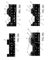
- the elementary MOS transistors 2 exhibit gate structures 12 comprising a gate oxide 7 comprising a thick central part 8 and lateral portions 9 with reduced thickness, as better highlighted in figure 13 .
- the profile of the gate oxide 7 and in particular of the central part 8 can be various and, in the case shown, it exhibits a squared shape substantially upturned T-like.
- the gate structures 12 comprise first gate conductive portions 13 overlapped onto the lateral portions 9 of the gate oxide 7 to define gate electrodes for the elementary MOS transistors 2.
- These first gate conductive portions 13 can also be realised with a double layer made of polysilicon and of a metallic silcide.
- the gate structures 12, as highlighted in figure 14 comprise a conductive structure 14, e.g. a mesh, suitable to distribute the signal coming from a gate pad or from a finger, suitably defined on the upper surface of the silicon plate and not highlighted in the figures.
- a conductive structure 14 e.g. a mesh, suitable to distribute the signal coming from a gate pad or from a finger, suitably defined on the upper surface of the silicon plate and not highlighted in the figures.
- the conductive structure 14 advantageously comprises second conductive portions 15 overlapped onto the thick central part 8 of the gate oxide 7 and suitably contained therein, interconnected to each other and to the first conductive portions 13 by a plurality of conductive bridges 16.
- the second conductive portions 15 and the conductive bridges 16 are realised in material such as for example polysilicon and they can be suitably doped.
- the second conductive portions 15 being placed above the central thick part 8 can be made very conductive further to hyper-doping.
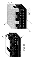
- these second conductive portions 15 can be realised in polysilicon suitably doped for being then, by means of suitable process, transformed, for the whole thickness or only for part thereof, into a metallic silicide 50 as highlighted in the embodiments reported in figures 22 and 23 .
- the second conductive portions 15 can be realised, entirely as highlighted in figure 19a , in a metallic layer 28 or, as highlighted in figure 19b , they can be realised in a metallic layer 28 overlapped onto a polysilicon layer 29.
- These realisations allow to improve the conductivity of the conductive structure 14, without jeopardising the functionality of the gate electrode or first conductive portions 13 being separated therefrom although connected by means of the conductive bridges 16.
- the conductive bridges 16 are transversally arranged between second consecutive conductive portions 15 and they comprise a flat portion 17, overlapped onto the semiconductor layer 4, and curved ends 18 arranged above the first conductive portions 13, thus allowing to connect them electrically.
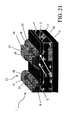
- each conductive bridge 16 can be partially interrupted or completely eliminated for reducing the capacities associated therewith as highlighted in figure 21 .
- the conductive bridges 16 further allow to electrically connect the second conductive portions 15 to the first underlying conductive portions 13 allowing an optimal distribution of the signal coming from the gate pad or from a gate finger to the elementary MOS transistors 2.
- the number and the mutual distance of the conductive bridges 16 allow to influence the speed of the power MOS device 1 and the propagation modes of the signal coming from the gate pad are thus suitably programmed and defined according to the needs.
- an insulating interconnection portion 19 realised in material such as for example oxide, which allows to avoid the electric contact between the two parts.
- one part or the entire insulating interconnection portion 19 can be realised simultaneously with the central part 8 of the gate oxide 7, thus exhibiting such a thickness as to allow an enormous gain on the capacities associated therewith.
- the body regions 10 of the elementary MOS transistors 2 are realised between two consecutive conductive bridges 16, they are insulated from each other and they exhibit a peripheral diffusion below the lateral portions 9 of the gate oxides 7 and below the consecutive conductive bridges 16 to define channel regions 21.
- the power MOS device 1 realised according to the present invention thus exhibits a gate structure 12 allowing to separate the transmission line of the signal in the power MOS device 1 by realising the conductive structure 14 from the gate electrodes by realising first conductive portions 13.
- a gate oxide 7 with double thickness allows to improve the dynamic operation of the power MOS device.
- each elementary MOS transistor 2 is connected to the gate pad or to a gate finger by means of the conductive structure 14 e.g. being a mesh, which is represented by a resistance given by the series of the resistances Rmesh and Rbridge and which is placed in parallel with the resistance of the first conductive portion 13, or gate electrode, indicated as Rpolgate.
- the conductive structure 14 e.g. being a mesh, which is represented by a resistance given by the series of the resistances Rmesh and Rbridge and which is placed in parallel with the resistance of the first conductive portion 13, or gate electrode, indicated as Rpolgate.
- the elementary MOS transistors 2 placed farther from the gate pad or from the gate finger will be made faster with respect to the a configuration according to the prior art wherein the conductive structure is also the gate electrode of the elementary MOS transistors 2 (R polgate ) as highlighted in figure 15 .
- the conductive structure is also the gate electrode of the elementary MOS transistors 2 (R polgate ) as highlighted in figure 15 .
- those placed closer to the gate pad or to the finger will be slowed down and this allows to uniform the time constant of the plurality of elementary MOS transistors 2 balancing the dynamic response of the power MOS device 1.
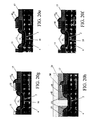
- the invention also relates to a method for realising a power MOS device shown making reference to figures 20a to 20h .
- the power MOS device realised is that shown in figures 22 and 23 and it is of the type comprising a plurality of elementary power MOS transistors 2.
- the realisation method according to the invention includes the following steps:
- the walls of the central part 8 of the gate oxide 7 can be very vertical to allow the formation of suitable polysilicon spacers.
- the interconnection portions 19 can be obtained simultaneously with the central parts 8 by means of the anisotropic etching to the thick oxide layer.
- the method further provides the stepsof: depositing, above the layer 4, a conductive layer 40 with thickness of about 200-800 nm (2000-8000 A) as highlighted in figure 20b .
- the conductive layer 40 realised for example in polysilicon, if necessary for the application, can be suitably doped; providing a photo-masking of the conductive layer 40, by placing a resist 41, to defined a conductive structure 14 of a gate structure 12 suitable to distribute a signal coming from a gate pad or from a finger, suitably defined on the upper surface of the silicon plate and not highlighted in the figures; anisotropically etching the conductive layer 40 to realise first conductive portions 13, of the gate structure 12, overlapped onto the lateral portions 9 of the gate oxide 7, as highlighted in figure 20c .
- the conductive structure 14 is of the type comprising a plurality of second conductive portions 15 overlapped onto the central part 8 of the gate oxide 7, and a plurality of conductive bridges 16 overlapped onto the interconnection portions 19.
- an anisotropic etching typology will be suitably used allowing to leave a residue, also called spacer, along the walls of the etched material. This allows to realise said first conductive portions 13 or gate electrodes of the elementary MOS transistors 2 self-aligned.
- the method then includes the step of:
- the conductive bridges 16 exhibit a flat portion 17, arranged transversally between consecutive first conductive portions 13 and two curved ends 18 which are placed above and transversally to said first conductive portions 13 to reach corresponding second conductive portions 15.
- the conductive bridges 16 thus allowing to electrically connect consecutive second conductive portions 15 to each other and to connect them to corresponding first portions 13.
- the method further includes the step of:
- the body regions 10, arranged between two consecutive conductive bridges 16 are insulated from each other and exhibit a peripheral diffusion below said lateral portions 9 of the gate oxide 7 and below the consecutive conductive bridges 16 to define channel regions 21.
- the method then includes the steps of:
- the method includes the following completion step:
- the method described according to the present invention allows to realise a power MOS device comprising a gate structure allowing to separate the gate electrode of the elementary MOS transistors 2 from the distribution mesh of the signal coming from the gate pad, such arrangement obtained by means of a synergy between the layout of the device and a process sequence.
- the method realised is applied to any power MOS device having a double gate oxide thickness on whose thick part a conductive structure is realised and by a conductive gate separated from said conductive structure and placed on the thin part of the gate oxide and being placed in electric connection with the conductive structure by means of suitable conductive bridges.
- Main advantage of the power MOS device obtained according to the present invention is that the gate structure allows, on one side, to separate the signal transmission mesh coming from the gate pad from the gate electrode of each elementary MOS transistor and, on the other, it allows, by using a gate oxide with double level, to harmonise the response during the dynamic step of the power MOS device.
- a further advantage of the present invention is that the conductive structure is completely self-aligned to the gate electrode of each elementary MOS transistor being obtained through deposition and etching steps. It is thus simpler to be realised and more precise without the use of alignment between masks.
- a further advantage of a MOS device realised by means of the present invention is the possibility of having a greater flexibility in the control of the gate resistance in relation to the number of the conductive bridges realised and to their mutual distance. In such way, by means of a suitable layout, it is possible to vary the switch speed of the power MOS device as well as the propagation mode of the driving signal according to the needs.
- the present invention allows to distribute the conduction bridges so that each area comprised between two consecutive bridges has the same highest gate resistance value R polgate and a minimal gate resistance value linearly depending on the distance from the gate pad or, if present, on the gate fingers or fingers.
- a further advantage linked to the separation between the conductive structure or mesh and the gate electrode of the elementary MOS transistors is that in such way the conductive material placed on the central part of the gate oxide can be transformed into a silicide avoiding all the problems linked to the faultiness or mechanical stress of the gate electrode which remains in conductive material such as polysilicon.
- the MOS device realised by means of the present invention employs a gate oxide with double thickness in technology VLSI keeping the compatibility with a partial or total silicidising process of the polysilicon.
Landscapes
- Electrodes Of Semiconductors (AREA)
- Metal-Oxide And Bipolar Metal-Oxide Semiconductor Integrated Circuits (AREA)
- Insulated Gate Type Field-Effect Transistor (AREA)
Claims (17)
- Leistungs-MOS-Vorrichtung des Typs, die eine Mehrzahl elementarer MOS-Leistungstransistoren (2) mit jeweiligen Gatestrukturen (12) auf einer Halbleiterschicht (4) aufweist, wobei jede Gatestruktur ein Gateoxid (7) mit einem dicken zentralen Teil (8) in direktem Kontakt mit lateralen Bereichen (9) reduzierter Dicke aufweist,
wobei die Gatestrukturen (12) Folgendes aufweisen:- erste leitfähige Bereiche (13), die die lateralen Bereiche (9) des Gateoxids (7) überlappend angeordnet sind, wobei die ersten leitfähigen Bereiche (13) für jeden der elementaren MOS-Transistoren (2) eine Gateelektrode bilden,- eine leitfähige Struktur (14), die mit einer Gateanschlussfläche oder einem Gatefinger der MOS-Vorrichtung (1) verbunden ist, um ein von der Gateanschlussfläche oder dem Gatefinger kommendes Signal zu verteilen, wobei die leitfähige Struktur (14) eine Mehrzahl von zweiten leitfähigen Bereiche (15) aufweist, die den dicken zentralen Teil (8) des Gateoxids (7) jedes elementaren MOS-Transistors (2) überlappend angeordnet sind;wobei die leitfähige Struktur (14) weiterhin eine Mehrzahl von leitfähigen Brücken (16) aufweist, die die zweiten leitfähigen Bereiche (15) miteinander verbinden und die zweiten leitfähigen Bereiche (15) mit den ersten leitfähigen Bereichen (13) verbinden, wobei die leitfähigen Brücken (16) gekrümmte Enden (18) aufweisen, die über und transversal zu den ersten leitfähigen Bereichen (13) angeordnet sind und eine elektrische Verbindung der zweiten leitfähigen Bereiche (15) mit den ersten leitfähigen Bereichen (13) ermöglichen;
wobei die Mehrzahl von leitfähigen Brücken (16) in einer Anzahl realisiert und in einem gegenseitigen Abstand in der leitfähigen Struktur (14) angeordnet sind, so dass die Zeitkonstante der Mehrzahl von elementaren MOS-Transistoren (2) einheitlich ist und dadurch das dynamische Ansprechen der MOS-Vorrichtung (1) ausgeglichen ist,
wobei die leitfähigen Brücken (16) derart verteilt sind, dass jeder Bereich der Gatestrukturen (16), der zwischen zwei aufeinander folgenden Brücken (16) vorhanden ist, den gleichen höchsten Gatewiderstandswert (Rpolgate) und einen minimalen Gatewiderstandswert in linearer Abhängigkeit von dem Abstand von der Gateanschlussfläche oder dem Gatefinger aufweist. - MOS-Vorrichtung nach Anspruch 1,
wobei die ersten leitfähigen Bereiche (13) in Polysilizium realisiert sind und den zentralen Teil (8) des Gateoxids (7) flankieren. - MOS-Vorrichtung nach Anspruch 1,
wobei die ersten leitfähigen Bereiche (13) in einer Doppelschicht realisiert sind, die aus Polysilizium und aus einem Metallsilizid gebildet ist. - MOS-Vorrichtung nach Anspruch 1,
wobei die leitfähigen Brücken (16) transversal zwischen zwei aufeinander folgenden der zweiten leitfähigen Bereich (15) angeordnet sind und einen flachen Bereich (17) aufweisen, der die Halbleiterschicht (4) und die gekrümmten Enden (18) überlappend angeordnet ist. - MOS-Vorrichtung nach Anspruch 4,
wobei zwischen den flachen Bereichen (17) der leitfähigen Brücken (16) und der Halbleiterschicht (4) jeweils ein isolierender Zwischenverbindungsbereich (19) vorhanden ist, der dafür geeignet ist, einen elektrischen Kontakt zwischen den jeweiligen flachen Bereichen (17) und der Halbleiterschicht (4) zu vermeiden. - MOS-Vorrichtung nach Anspruch 5,
wobei die isolierenden Zwischenverbindungsbereiche (19) mittels einer Oxidschicht realisiert sind. - MOS-Vorrichtung nach Anspruch 6,
wobei die isolierenden Zwischenverbindungsbereiche (19) die jeweiligen lateralen Bereiche (9) des Gateoxids (7) transversal miteinander verbinden. - MOS-Vorrichtung nach einem oder mehreren der vorausgehenden Ansprüche,
wobei die zweiten leitfähigen Bereiche (15) und die leitfähigen Brücken (16) in Polysilizium realisiert sind. - MOS-Vorrichtung nach einem oder mehreren der vorausgehenden Ansprüche,
wobei die zweiten leitfähigen Bereiche (15) und/oder die leitfähigen Brücken (16) dotiert sind. - MOS-Vorrichtung nach Anspruch 1,
wobei die zweiten leitfähigen Bereiche (15) in einer Doppelschicht realisiert sind, die aus Polysilizium und aus einem Metallsilizid gebildet ist. - MOS-Vorrichtung nach Anspruch 1,
wobei die zweiten leitfähigen Bereiche (15) in einer Metallsilizidschicht realisiert sind. - MOS-Vorrichtung nach Anspruch 1,
wobei die zweiten leitfähigen Bereiche (15) in einer metallischen Schicht realisiert sind. - MOS-Vorrichtung nach einem oder mehreren der vorausgehenden Ansprüche,
wobei die elementaren MOS-Transistoren (2) Körperbereiche (10) und einen oben enthaltenen Sourcebereich (11) aufweisen, wobei die Körperbereiche (10) zwischen zwei aufeinander folgenden der leitfähigen Brücken (16) realisiert sind, voneinander isoliert sind und eine periphere Diffusion unter den lateralen Bereichen (9) der Gateoxide (7) sowie unter den aufeinander folgenden leitfähigen Brücken (16) aufweisen, um Kanalbereiche (21) zu bilden. - Verfahren zum Realisieren einer Leistungs-MOS-Vorrichtung des Typs mit einer Mehrzahl von elementaren MOS-Leistungstransistoren (2), wobei das Verfahren folgende Schritte aufweist:- Wachsen-Lassen einer dicken Oxidschicht aus einer Halbleiterschicht (4) einer Siliziumplatte;- Vorsehen einer Fotomaske durch Platzieren eines Resist auf der dicken Oxidschicht, um eine Mehrzahl von Gateoxidteilen zu bilden;- anisotropes Ätzen der dicken Oxidschicht und Realisieren einer Mehrzahl von dicken Gateoxidteilen (8);- Entfernen der Maske;- Realisieren einer dünneren Gateoxidschicht in Bezug auf die dicke Oxidschicht, um Gateoxidbereiche (9) seitlich von den dicken Gateoxidteilen (8) zu bilden;
wobei das gebildete Gateoxid (7) dadurch einen dicken zentralen Teil (8) in direktem Kontakt mit lateralen Bereichen (9) mit reduzierter Dicke für jeden elementaren MOS-Leistungstransistor aufweist,
wobei das Verfahren ferner Folgende Schritte aufweist:- Aufbringen einer leitfähigen Schicht (40) oben auf dem Gateoxid (7);- Vorsehen einer Fotomaske an der leitfähigen Schicht durch Platzieren eines Resist (41), um eine Gatestruktur (12) zu bilden, die eine leitfähige Struktur (14) des Typs mit einer Mehrzahl von zweiten leitfähigen Bereichen (15) aufweist, die die dicken zentralen Teile (8) des Gateoxids (7) überlappend angeordnet sind, und- anisotropes Ätzen der leitfähigen Schicht (20) unter Bildung von Rückständen, um eine Mehrzahl von ersten leitfähigen Bereichen (13) zu bilden, die die lateralen Bereiche (9) überlappend angeordnet sind, wobei die ersten leitfähigen Bereiche (13) für jeden der elementaren MOS-Transistoren (2) eine Gateelektrode bilden;- Entfernen des Resist (41);
wobei die Gatestruktur (12) die Mehrzahl der ersten leitfähigen Bereiche (13) aufweist, die die lateralen Bereiche (9) der Gatestruktur (7) überlappend angeordnet sind, und die leitfähige Struktur (14) mit einer Gateanschlussfläche oder einem Gatefinger der Vorrichtung verbunden wird, um ein von der Gateanschlussfläche oder dem Gatefinger kommendes Signal zu verteilen, wobei die leitfähige Struktur (14) die Mehrzahl der zweiten leitfähigen Bereiche (15) aufweist, die die dicken zentralen Teile (8) des Gateoxids (7) überlappend angeordnet sind,
wobei der Schritt des anisotropen Ätzens der leitfähigen Schicht (40) auch eine Mehrzahl von leitfähigen Brücken (16) der leitfähigen Struktur (14) bildet, die die zweiten leitfähigen Bereiche (15) miteinander verbinden und die zweiten leitfähigen Bereiche (15) mit den ersten leitfähigen Bereichen (13) verbinden;
wobei die Mehrzahl der leitfähigen Brücken (16) gekrümmte Enden (18) aufweisen, die über und transversal zu den ersten leitfähigen Bereichen (13) angeordnet sind und eine elektrische Verbindung der zweiten leitfähigen Bereiche (15) mit den ersten leitfähigen Bereichen (13) ermöglichen, wobei die Mehrzahl der leitfähigen Brücken (16) in einer Anzahl realisiert und in einem gegenseitigen Abstand in der leitfähigen Struktur (14) angeordnet sind, so dass die Zeitkonstante der Mehrzahl von elementaren MOS-Transistoren (2) einheitlich ist und dadurch das dynamische Ansprechen der MOS-Vorrichtung (1) ausgeglichen ist,
wobei die leitfähigen Brücken (16) derart verteilt sind, dass jeder Bereich der Gatestrukturen (16), der zwischen zwei aufeinander folgenden Brücken (16) vorhanden ist, den gleichen höchsten Gatewiderstandswert (Rpolgate) und einen minimalen Gatewiderstandswert in linearer Abhängigkeit von dem Abstand von der Gateanschlussfläche oder dem Gatefinger aufweist. - Verfahren nach Anspruch 14,
wobei die leitfähigen Brücken (16) in einer Mehrzahl von isolierenden Zwischenverbindungsbereichen (19) überlappend vorgesehen werden, wobei die Zwischenverbindungsbereiche (19) jeweilige laterale Bereiche (9) des Gateoxids (7) transversal miteinander verbinden. - Verfahren nach Anspruch 15,
wobei die Zwischenverbindungsbereiche (19) während des anisotropen Ätzschrittes der dicken Oxidschicht realisiert werden. - Verfahren nach einem der Ansprüche 14 bis 16,
wobei das Verfahren ferner folgende Schritte aufweist:- Bilden einer Mehrzahl von Körper-Wannen zum Realisieren von Körperbereichen (10) und Source-Wannen zum Realisieren von Source-Bereichen (11) der elementaren MOS-Transistoren (2), wobei die Körperbereiche (10) zwischen zwei aufeinander folgenden der leitfähigen Brücken (16) angeordnet werden, voneinander isoliert sind und eine periphere Diffusion unter den lateralen Bereichen (9) der Gateoxide (7) und unter den aufeinander folgenden leitfähigen Brücken (16) aufweisen, um Kanalbereiche (21) zu bilden, und wobei das Verfahren ferner folgende Schritte aufweist:- Aufbringen einer Isolierschicht (45) geeigneter Dicke;- Vorsehen einer Fotomaske an der Isolierschicht, um geeignete Silizidierungsbereiche insbesondere an dem oberen Teil der aus Silizium gebildeten, zweiten leitfähigen Bereiche (15) zu bilden;- Aufbringen einer geeigneten metallischen Schicht (46);- Ausführen eines thermischen Prozesses oder eines anderen Prozesses, der geeignet ist, die metallische Schicht (46) mit dem unbedeckten Silizium reagieren zu lassen, um dadurch eine Silizidschicht (50) zu bilden;- Ätzen und Eliminieren eines Bereichs der unreagierten metallischen Schicht (46);- Bedecken der Siliziumplatte mit einer zwischengeordneten dielektrischen Schicht (47) und Bilden von Metallisierungen (48) an der Vorderseite sowie am Rest der Platte.
Applications Claiming Priority (1)
| Application Number | Priority Date | Filing Date | Title |
|---|---|---|---|
| IT002244A ITMI20042244A1 (it) | 2004-11-19 | 2004-11-19 | Dispositivo elettronico mos di potenza e relativo metodo di realizzazione |
Publications (2)
| Publication Number | Publication Date |
|---|---|
| EP1659638A1 EP1659638A1 (de) | 2006-05-24 |
| EP1659638B1 true EP1659638B1 (de) | 2011-01-12 |
Family
ID=35597212
Family Applications (1)
| Application Number | Title | Priority Date | Filing Date |
|---|---|---|---|
| EP05025288A Expired - Lifetime EP1659638B1 (de) | 2004-11-19 | 2005-11-18 | MOS-Leistungsanordnung und entsprechendes Herstellungsverfahren |
Country Status (3)
| Country | Link |
|---|---|
| EP (1) | EP1659638B1 (de) |
| DE (1) | DE602005025846D1 (de) |
| IT (1) | ITMI20042244A1 (de) |
Families Citing this family (1)
| Publication number | Priority date | Publication date | Assignee | Title |
|---|---|---|---|---|
| US20130154017A1 (en) * | 2011-12-14 | 2013-06-20 | Microchip Technology Incorporated | Self-Aligned Gate Structure for Field Effect Transistor |
Family Cites Families (4)
| Publication number | Priority date | Publication date | Assignee | Title |
|---|---|---|---|---|
| US5510281A (en) | 1995-03-20 | 1996-04-23 | General Electric Company | Method of fabricating a self-aligned DMOS transistor device using SiC and spacers |
| JP3166148B2 (ja) | 1995-07-11 | 2001-05-14 | 横河電機株式会社 | 半導体装置 |
| GB9726829D0 (en) | 1997-12-19 | 1998-02-18 | Philips Electronics Nv | Power semiconductor devices |
| US6756644B2 (en) * | 2001-03-28 | 2004-06-29 | International Rectifier Corporation | Ultra low QGD power MOSFET |
-
2004
- 2004-11-19 IT IT002244A patent/ITMI20042244A1/it unknown
-
2005
- 2005-11-18 EP EP05025288A patent/EP1659638B1/de not_active Expired - Lifetime
- 2005-11-18 DE DE602005025846T patent/DE602005025846D1/de not_active Expired - Lifetime
Also Published As
| Publication number | Publication date |
|---|---|
| EP1659638A1 (de) | 2006-05-24 |
| DE602005025846D1 (de) | 2011-02-24 |
| ITMI20042244A1 (it) | 2005-02-19 |
Similar Documents
| Publication | Publication Date | Title |
|---|---|---|
| US8420487B2 (en) | Power MOS electronic device and corresponding realizing method | |
| US8637369B2 (en) | Method for manufacturing an integrated power device having gate structures within trenches | |
| TW437066B (en) | Mosgated device with trench structure and remote contact and process for its manufacture | |
| CN101512773B (zh) | 以密闭式晶胞结构增加信道密度的次微米平面半导体功率器件 | |
| US5592006A (en) | Gate resistor for IGBT | |
| KR19980041853A (ko) | 감소된 게이트 저항을 갖는 멀티-핑거 모스 트랜지스터 | |
| EP0730309B1 (de) | Hochspannungs-MOSFET mit Feldplatten-Elektrode und Verfahren zur Herstellung | |
| EP1408552A1 (de) | Integriertes MOS-Halbleiterbauelement mit grosser Leistungsfähigkeit und Verfahren zu seiner Herstellung | |
| KR20050008223A (ko) | 리세스된 게이트 전극을 갖는 반도체 소자의 집적방법 | |
| EP0729647A1 (de) | Diamantförmige gate-zelle für mos-transistormatrix | |
| US6955970B1 (en) | Process for manufacturing a low voltage MOSFET power device having a minimum figure of merit | |
| EP1659638B1 (de) | MOS-Leistungsanordnung und entsprechendes Herstellungsverfahren | |
| US5888889A (en) | Integrated structure pad assembly for lead bonding | |
| US7508027B2 (en) | Single-poly EPROM device and method of manufacturing | |
| WO2001031711A2 (en) | Vertical insulated gate field-effect device and method of making the same | |
| WO2003107432A1 (en) | Power semiconductor device and method of manufacturing the same | |
| EP0463511B1 (de) | Verfahren zum Herstellen einer EPROM-Zelle mit geteiltem Gate und mit Polysilizium-Abstandhaltern | |
| EP1659636B1 (de) | MOS-Leistungshalbleiteranordnung | |
| EP1503423B1 (de) | Verfahren zur Herstellung einer MIS-Leistungshalbleiteranordnung | |
| US20040067610A1 (en) | RF semiconductor devices and methods for fabricating the same | |
| CN117476598A (zh) | 功率器件的金属互连结构和制造方法 | |
| KR960043301A (ko) | 불휘발성 메모리 장치 및 그 제조방법 | |
| JPH04245682A (ja) | 電界効果トランジスタ | |
| WO2006122957A2 (en) | Mos power device with high integration density and manufacturing process thereof | |
| JPS6214470A (ja) | 縦形半導体装置およびその製造方法 |
Legal Events
| Date | Code | Title | Description |
|---|---|---|---|
| PUAI | Public reference made under article 153(3) epc to a published international application that has entered the european phase |
Free format text: ORIGINAL CODE: 0009012 |
|
| AK | Designated contracting states |
Kind code of ref document: A1 Designated state(s): AT BE BG CH CY CZ DE DK EE ES FI FR GB GR HU IE IS IT LI LT LU LV MC NL PL PT RO SE SI SK TR |
|
| AX | Request for extension of the european patent |
Extension state: AL BA HR MK YU |
|
| 17P | Request for examination filed |
Effective date: 20061123 |
|
| AKX | Designation fees paid |
Designated state(s): DE FR GB IT |
|
| 17Q | First examination report despatched |
Effective date: 20070115 |
|
| RAP1 | Party data changed (applicant data changed or rights of an application transferred) |
Owner name: STMICROELECTRONICS SRL |
|
| RIC1 | Information provided on ipc code assigned before grant |
Ipc: H01L 29/78 20060101AFI20100422BHEP Ipc: H01L 29/49 20060101ALN20100422BHEP Ipc: H01L 21/28 20060101ALN20100422BHEP Ipc: H01L 29/423 20060101ALI20100422BHEP Ipc: H01L 21/336 20060101ALI20100422BHEP |
|
| GRAP | Despatch of communication of intention to grant a patent |
Free format text: ORIGINAL CODE: EPIDOSNIGR1 |
|
| GRAS | Grant fee paid |
Free format text: ORIGINAL CODE: EPIDOSNIGR3 |
|
| GRAA | (expected) grant |
Free format text: ORIGINAL CODE: 0009210 |
|
| AK | Designated contracting states |
Kind code of ref document: B1 Designated state(s): DE FR GB IT |
|
| REG | Reference to a national code |
Ref country code: GB Ref legal event code: FG4D |
|
| REF | Corresponds to: |
Ref document number: 602005025846 Country of ref document: DE Date of ref document: 20110224 Kind code of ref document: P |
|
| REG | Reference to a national code |
Ref country code: DE Ref legal event code: R096 Ref document number: 602005025846 Country of ref document: DE Effective date: 20110224 |
|
| PLBE | No opposition filed within time limit |
Free format text: ORIGINAL CODE: 0009261 |
|
| STAA | Information on the status of an ep patent application or granted ep patent |
Free format text: STATUS: NO OPPOSITION FILED WITHIN TIME LIMIT |
|
| 26N | No opposition filed |
Effective date: 20111013 |
|
| REG | Reference to a national code |
Ref country code: DE Ref legal event code: R097 Ref document number: 602005025846 Country of ref document: DE Effective date: 20111013 |
|
| GBPC | Gb: european patent ceased through non-payment of renewal fee |
Effective date: 20111118 |
|
| PG25 | Lapsed in a contracting state [announced via postgrant information from national office to epo] |
Ref country code: GB Free format text: LAPSE BECAUSE OF NON-PAYMENT OF DUE FEES Effective date: 20111118 |
|
| PG25 | Lapsed in a contracting state [announced via postgrant information from national office to epo] |
Ref country code: IT Free format text: LAPSE BECAUSE OF NON-PAYMENT OF DUE FEES Effective date: 20121118 |
|
| PGFP | Annual fee paid to national office [announced via postgrant information from national office to epo] |
Ref country code: FR Payment date: 20131121 Year of fee payment: 9 |
|
| REG | Reference to a national code |
Ref country code: FR Ref legal event code: ST Effective date: 20150731 |
|
| PG25 | Lapsed in a contracting state [announced via postgrant information from national office to epo] |
Ref country code: FR Free format text: LAPSE BECAUSE OF NON-PAYMENT OF DUE FEES Effective date: 20141201 |
|
| REG | Reference to a national code |
Ref country code: DE Ref legal event code: R079 Ref document number: 602005025846 Country of ref document: DE Free format text: PREVIOUS MAIN CLASS: H01L0029780000 Ipc: H10D0030600000 |
|
| PGFP | Annual fee paid to national office [announced via postgrant information from national office to epo] |
Ref country code: DE Payment date: 20241022 Year of fee payment: 20 |
|
| REG | Reference to a national code |
Ref country code: DE Ref legal event code: R071 Ref document number: 602005025846 Country of ref document: DE |